EP4435851A2 - Semiconductor device - Google Patents
Semiconductor device Download PDFInfo
- Publication number
- EP4435851A2 EP4435851A2 EP24163968.1A EP24163968A EP4435851A2 EP 4435851 A2 EP4435851 A2 EP 4435851A2 EP 24163968 A EP24163968 A EP 24163968A EP 4435851 A2 EP4435851 A2 EP 4435851A2
- Authority
- EP
- European Patent Office
- Prior art keywords
- lid
- semiconductor die
- semiconductor device
- top surface
- gel
- Prior art date
- Legal status (The legal status is an assumption and is not a legal conclusion. Google has not performed a legal analysis and makes no representation as to the accuracy of the status listed.)
- Pending
Links
Images




Classifications
-
- H—ELECTRICITY
- H10—SEMICONDUCTOR DEVICES; ELECTRIC SOLID-STATE DEVICES NOT OTHERWISE PROVIDED FOR
- H10W—GENERIC PACKAGES, INTERCONNECTIONS, CONNECTORS OR OTHER CONSTRUCTIONAL DETAILS OF DEVICES COVERED BY CLASS H10
- H10W40/00—Arrangements for thermal protection or thermal control
- H10W40/20—Arrangements for cooling
- H10W40/25—Arrangements for cooling characterised by their materials
- H10W40/258—Metallic materials
-
- H—ELECTRICITY
- H10—SEMICONDUCTOR DEVICES; ELECTRIC SOLID-STATE DEVICES NOT OTHERWISE PROVIDED FOR
- H10W—GENERIC PACKAGES, INTERCONNECTIONS, CONNECTORS OR OTHER CONSTRUCTIONAL DETAILS OF DEVICES COVERED BY CLASS H10
- H10W40/00—Arrangements for thermal protection or thermal control
- H10W40/20—Arrangements for cooling
- H10W40/22—Arrangements for cooling characterised by their shape, e.g. having conical or cylindrical projections
-
- H—ELECTRICITY
- H10—SEMICONDUCTOR DEVICES; ELECTRIC SOLID-STATE DEVICES NOT OTHERWISE PROVIDED FOR
- H10W—GENERIC PACKAGES, INTERCONNECTIONS, CONNECTORS OR OTHER CONSTRUCTIONAL DETAILS OF DEVICES COVERED BY CLASS H10
- H10W40/00—Arrangements for thermal protection or thermal control
- H10W40/70—Fillings or auxiliary members in containers or in encapsulations for thermal protection or control
-
- H—ELECTRICITY
- H10—SEMICONDUCTOR DEVICES; ELECTRIC SOLID-STATE DEVICES NOT OTHERWISE PROVIDED FOR
- H10W—GENERIC PACKAGES, INTERCONNECTIONS, CONNECTORS OR OTHER CONSTRUCTIONAL DETAILS OF DEVICES COVERED BY CLASS H10
- H10W74/00—Encapsulations, e.g. protective coatings
- H10W74/10—Encapsulations, e.g. protective coatings characterised by their shape or disposition
- H10W74/111—Encapsulations, e.g. protective coatings characterised by their shape or disposition the semiconductor body being completely enclosed
- H10W74/114—Encapsulations, e.g. protective coatings characterised by their shape or disposition the semiconductor body being completely enclosed by a substrate and the encapsulations
- H10W74/117—Encapsulations, e.g. protective coatings characterised by their shape or disposition the semiconductor body being completely enclosed by a substrate and the encapsulations the substrate having spherical bumps for external connection
-
- H—ELECTRICITY
- H10—SEMICONDUCTOR DEVICES; ELECTRIC SOLID-STATE DEVICES NOT OTHERWISE PROVIDED FOR
- H10W—GENERIC PACKAGES, INTERCONNECTIONS, CONNECTORS OR OTHER CONSTRUCTIONAL DETAILS OF DEVICES COVERED BY CLASS H10
- H10W76/00—Containers; Fillings or auxiliary members therefor; Seals
- H10W76/10—Containers or parts thereof
- H10W76/12—Containers or parts thereof characterised by their shape
-
- H—ELECTRICITY
- H10—SEMICONDUCTOR DEVICES; ELECTRIC SOLID-STATE DEVICES NOT OTHERWISE PROVIDED FOR
- H10W—GENERIC PACKAGES, INTERCONNECTIONS, CONNECTORS OR OTHER CONSTRUCTIONAL DETAILS OF DEVICES COVERED BY CLASS H10
- H10W76/00—Containers; Fillings or auxiliary members therefor; Seals
- H10W76/60—Seals
-
- H—ELECTRICITY
- H10—SEMICONDUCTOR DEVICES; ELECTRIC SOLID-STATE DEVICES NOT OTHERWISE PROVIDED FOR
- H10W—GENERIC PACKAGES, INTERCONNECTIONS, CONNECTORS OR OTHER CONSTRUCTIONAL DETAILS OF DEVICES COVERED BY CLASS H10
- H10W40/00—Arrangements for thermal protection or thermal control
- H10W40/20—Arrangements for cooling
- H10W40/22—Arrangements for cooling characterised by their shape, e.g. having conical or cylindrical projections
- H10W40/226—Arrangements for cooling characterised by their shape, e.g. having conical or cylindrical projections characterised by projecting parts, e.g. fins to increase surface area
- H10W40/228—Arrangements for cooling characterised by their shape, e.g. having conical or cylindrical projections characterised by projecting parts, e.g. fins to increase surface area the projecting parts being wire-shaped or pin-shaped
-
- H—ELECTRICITY
- H10—SEMICONDUCTOR DEVICES; ELECTRIC SOLID-STATE DEVICES NOT OTHERWISE PROVIDED FOR
- H10W—GENERIC PACKAGES, INTERCONNECTIONS, CONNECTORS OR OTHER CONSTRUCTIONAL DETAILS OF DEVICES COVERED BY CLASS H10
- H10W74/00—Encapsulations, e.g. protective coatings
- H10W74/10—Encapsulations, e.g. protective coatings characterised by their shape or disposition
- H10W74/15—Encapsulations, e.g. protective coatings characterised by their shape or disposition on active surfaces of flip-chip devices, e.g. underfills
-
- H—ELECTRICITY
- H10—SEMICONDUCTOR DEVICES; ELECTRIC SOLID-STATE DEVICES NOT OTHERWISE PROVIDED FOR
- H10W—GENERIC PACKAGES, INTERCONNECTIONS, CONNECTORS OR OTHER CONSTRUCTIONAL DETAILS OF DEVICES COVERED BY CLASS H10
- H10W76/00—Containers; Fillings or auxiliary members therefor; Seals
- H10W76/10—Containers or parts thereof
-
- H—ELECTRICITY
- H10—SEMICONDUCTOR DEVICES; ELECTRIC SOLID-STATE DEVICES NOT OTHERWISE PROVIDED FOR
- H10W—GENERIC PACKAGES, INTERCONNECTIONS, CONNECTORS OR OTHER CONSTRUCTIONAL DETAILS OF DEVICES COVERED BY CLASS H10
- H10W76/00—Containers; Fillings or auxiliary members therefor; Seals
- H10W76/60—Seals
- H10W76/63—Seals characterised by their shape or disposition, e.g. between cap and walls of a container
-
- H—ELECTRICITY
- H10—SEMICONDUCTOR DEVICES; ELECTRIC SOLID-STATE DEVICES NOT OTHERWISE PROVIDED FOR
- H10W—GENERIC PACKAGES, INTERCONNECTIONS, CONNECTORS OR OTHER CONSTRUCTIONAL DETAILS OF DEVICES COVERED BY CLASS H10
- H10W90/00—Package configurations
- H10W90/701—Package configurations characterised by the relative positions of pads or connectors relative to package parts
- H10W90/721—Package configurations characterised by the relative positions of pads or connectors relative to package parts of bump connectors
- H10W90/724—Package configurations characterised by the relative positions of pads or connectors relative to package parts of bump connectors between a chip and a stacked insulating package substrate, interposer or RDL
-
- H—ELECTRICITY
- H10—SEMICONDUCTOR DEVICES; ELECTRIC SOLID-STATE DEVICES NOT OTHERWISE PROVIDED FOR
- H10W—GENERIC PACKAGES, INTERCONNECTIONS, CONNECTORS OR OTHER CONSTRUCTIONAL DETAILS OF DEVICES COVERED BY CLASS H10
- H10W90/00—Package configurations
- H10W90/701—Package configurations characterised by the relative positions of pads or connectors relative to package parts
- H10W90/731—Package configurations characterised by the relative positions of pads or connectors relative to package parts of die-attach connectors
- H10W90/734—Package configurations characterised by the relative positions of pads or connectors relative to package parts of die-attach connectors between a chip and a stacked insulating package substrate, interposer or RDL
Definitions
- the present disclosure relates to a semiconductor device and, in particular, to a semiconductor device including a liquid metal.
- Conventional semiconductor device includes a substrate and an electronic component disposed on the substrate.
- the electronic component inevitably generates heat during operation.
- how to dissipate the heat from the electronic component has become a prominent task for the industry.
- An embodiment of the present disclosure provides a semiconductor device.
- the semiconductor device includes a substrate, a semiconductor die, a lid, a liquid metal, a gel and a thermal dissipation structure.
- the semiconductor die is disposed on the substrate.
- the lid is disposed on the substrate and covers the semiconductor die.
- the lid has an opening to expose the semiconductor die.
- the liquid metal is disposed on the semiconductor die.
- the gel is disposed between the semiconductor die and the lid.
- the thermal dissipation structure is disposed on the lid and covers the liquid metal.
- the semiconductor die, the gel and the thermal dissipation structure form a closed space for accommodating the liquid metal.
- the lid comprises an extending portion extending towards the semiconductor die, and the gel is in contact with the extending portion of the lid to seal a gap between the semiconductor die and the extending portion.
- a bottom surface of the extending portion is higher than or flush with a top surface of the semiconductor die.
- a top surface of the thermal dissipation structure is flush with a top surface of the lid.
- the thermal dissipation structure has a protrusion portion protruding from a bottom surface and/or a top surface of the thermal dissipation structure.
- a bottom surface of the extending portion is lower than a top surface of the semiconductor die; and/or a top surface of the extending portion is flush with the top surface of the semiconductor die.
- the thermal dissipation structure comprises a metal plate or a heat sink.
- the gel is affixed to the thermal dissipation structure.
- the thermal dissipation structure covers a top surface of the extending portion, and the gel fills a gap between the thermal dissipation structure and the top surface of the extending portion.
- the gel fills a recess of thermal dissipation structure, wherein the recess is recessed from a bottom surface of the thermal dissipation structure. In some embodiments, the gel is arranged on an edge of a top surface of the semiconductor die. In some embodiments, the semiconductor device further includes conductive structures disposed between the substrate and the semiconductor die. In some embodiments, the semiconductor device further includes an underfill arranged between the substrate and the semiconductor die and surrounding the conductive elements. In some embodiments, the lid is arranged on the substrate by an adhesive. In some embodiments, the thermal dissipation structure is arranged on the lid by an adhesive. In some embodiments, the semiconductor device further includes a molding compound surrounding the semiconductor die.
- the gel is arranged on an edge of a top surface of the molding compound.
- the liquid metal is in contact with an entire top surface of the semiconductor die.
- a bottom surface of the extending portion is higher than or flush with a top surface of the semiconductor die; or the bottom surface of the extending portion is lower than the top surface of the semiconductor die.
- a top surface of the extending portion is flush with a top surface of the semiconductor die.
- An embodiment of the present disclosure provides a semiconductor device.
- the semiconductor device includes a substrate, a semiconductor die, a molding compound, a lid, a gel and a liquid metal.
- the semiconductor die is disposed on the substrate.
- the lid is disposed on the substrate and covers the semiconductor die and the molding compound.
- the gel is arranged between the molding compound and the lid.
- the liquid metal is arranged between an entire top surface of the semiconductor die and the lid.
- the semiconductor die, the lid, the gel and the thermal dissipation structure form a closed space for accommodating the liquid metal.
- the lid has a recess on a bottom surface of the lid; or the lid has a protrusion portion protruding from the bottom surface of the lid. In some embodiments, the lid is an integrated structure.
- FIGS. 1, 2 , 3, 4 , 5, 6 , 7, 8 , 9, 10 , 11, 12 , 13, 14 , 15 and 16 are cross-sectional views of a semiconductor device in accordance with some embodiments of the disclosure.
- inventive concept is described fully hereinafter with reference to the accompanying drawings, in which exemplary embodiments of the inventive concept are shown.
- the advantages and features of the inventive concept and methods of achieving them will be apparent from the following exemplary embodiments that will be described in more detail with reference to the accompanying drawings.
- inventive concept is not limited to the following exemplary embodiments, and may be implemented in various forms. Accordingly, the exemplary embodiments are provided only to disclose the inventive concept and let those skilled in the art know the category of the inventive concept.
- the drawings as illustrated are only schematic and are nonlimiting. In the drawings, the size of some of the elements may be exaggerated for illustrative purposes and not drawn to scale. The dimensions and the relative dimensions do not correspond to actual dimensions in the practice of the disclosure.
- TIM 1 thermal interface material 1
- LMs liquid metals
- the liquid metal used in TIM1 applications may easily spread to undesired spaces and further cause coverage issue and circuit short problem while touching the substrate or electronic components (such as semiconductor dies/capacitors/resistors/inductors).
- the liquid metal When the temperature rises or the semiconductor device isn't fixed horizontally, the liquid metal will flow outside, and further pollute the substrate or other components (such as semiconductor dies/capacitors/resistors/inductors). Thus, a novel semiconductor device that includes a liquid metal is desirable.
- FIG. 1 is a cross-sectional view of a semiconductor device 500A in accordance with some embodiments of the disclosure.
- the semiconductor device 500A is a portion of mobile phones, personal digital assistants (PDA), digital cameras, and servers, etc..
- the semiconductor device 500A is capable of applying to (or disposed on) a package requiring high-power operation, such as flip chip ball grid array (FCBGA), land grid array (LGA), fan-out package, three-dimensional (3D) integrated circuit (IC) package, etc.
- the semiconductor device 500A includes a substrate 200, a semiconductor die 210, a lid 220A, a liquid metal 224, a gel 222 and a thermal dissipation structure 230A.
- the substrate 200 can be a single layer or a multilayer structure.
- the substrate 200 is, for example, a printed circuit board (PCB), an interposer, a package substrate, another semiconductor device or a semiconductor package.
- the substrate 200 may be formed of dielectric materials (e.g., polypropylene (PP), epoxy, polyimide, or other applicable resin materials) or semiconductor materials.
- the substrate 200 has a top surface 200T and a bottom surface 200B opposite the top surface 200T.
- the substrate 200 is provided for the semiconductor die 210 disposed on the top surface 200T.
- a plurality of conductive traces (not shown), conductive vias and/or conductive pads (not shown) are disposed in the substrate 200.
- the conductive traces may be electrically connected to the corresponding conductive vias and conductive pads.
- the conductive pads and/or the conductive traces are exposed to openings of solder mask layers (not shown) disposed close to the top surface 200T and the bottom surface 200B.
- the conductive traces may comprise signal trace segments or ground trace segments, which are used for the input/output (I/O) connections of the semiconductor die 210.
- the conductive pads are disposed on the top surface 200T of the substrate 200, connected to different terminals of the conductive traces. The conductive pads are used for the semiconductor die 210 that is mounted directly on them.
- the semiconductor device 500A further includes conductive structures 204 disposed on the bottom surface 200B of substrate 200 away from the semiconductor die 210 and in contact with the corresponding the conductive pads (not shown) of the substrate 200.
- the conductive structures 204 includes a conductive ball structure such as a solder ball, copper-core solder ball, a conductive bump structure such as a copper bump or a solder bump structure, or a conductive pillar structure such as a copper pillar structure.
- the semiconductor die 210 is flipped to be disposed on the substrate 200 opposite the conductive structures 204 by a bonding process.
- the semiconductor die 210 is mounted on the substrate 200 using conductive structures 216.
- the semiconductor die 210 is electrically connected to the conductive structures 204 by the substrate 200.
- the semiconductor die 210 is, for example, a fan-out semiconductor die, such a central processing unit (CPU), a graphic processing unit (GPU), a dynamic random access memory (DRAM) controller or any combination thereof.
- the semiconductor die 210 is fabricated by a flip-chip technology.
- the conductive structures 216 are electrically connected to the conductive pads (including conductive traces) of the substrate 200.
- the conductive structures 216 include a conductive ball structure such as a solder ball, copper-core solder ball, a conductive bump structure such as a copper bump or a solder bump structure, or a conductive pillar structure such as a copper pillar structure.
- one of the conductive structures 216 may include a conductive pillar structure 212 and a conductive bump structure 214.
- the semiconductor device 500A further includes an underfill 218 arranged between the substrate 200 and the semiconductor die 210.
- the underfill 218 surrounds the conductive elements 216.
- the underfill 218 fills the gap (not shown) between the substrate 200 and the semiconductor die 210.
- the underfill 218 covers a bottom surface 210B of the semiconductor die 210 and the top surface 200T of substrate 200.
- the underfill 218 is also in contact with the bottom surface 210B of the semiconductor die 210 and the top surface 200T of substrate 200.
- the underfill 218 may help to dissipate heat generated from the semiconductor die 210 and to reduce the thermal resistance from the semiconductor die 210 to the substrate 200.
- the underfill 218 surrounds and covers side surfaces 2105 of the semiconductor die 210.
- the underfill 218 may be in contact with the side surfaces 2105 of the semiconductor die 210.
- the underfill 218 may help stabilize the semiconductor die 210.
- the lid 220A is disposed on the substrate 200.
- the lid 220A is disposed so that it surrounds and covers side surfaces 2105 of the semiconductor die 210.
- the lid 220A may also surround and cover the underfill 218.
- the lid 220A and the underfill 218 may not be in contact with each other.
- the lid 220A includes an extending portion 220A-E extending towards the semiconductor die 210. The extending portion 220A-E may also cover the space between the lid 220A and the underfill 218.
- the extending portion 220A-E has an opening 221 (or a through hole) directly above the semiconductor die 210 to expose an entire top surface 210T of the semiconductor die 210.
- the extending portion 220A-E has a top surface 220AT and a bottom surface 220A-EB.
- the top surface 220AT may also serve as the top surface of the lid 220A.
- the bottom surface 220A-EB of the extending portion 220A-E is higher than or flush with the top surface 210T of the semiconductor die 210.
- the lid 220A may be made by a metal material, such as copper, aluminum, iron or a combination thereof.
- the lid 220A may be made by a non-metal material, such as a ceramic material, a polymer material or another applicable non-metal material.
- the lid 220A could conduct heat and increase strength of the semiconductor device 500A for reducing warpage.
- the semiconductor device 500A further includes an adhesive 208 disposed between the lid 220A and the on the top surface 200T of the substrate 200, so that the lid 220A is arranged on the top surface 200T of the substrate 200.
- the gel 222 is disposed between the semiconductor die 210 and the lid 220A.
- the gel 222 may be arranged on an edge of the top surface 210T of the semiconductor die 210.
- the gel 222 may be in contact with a side surface 220A-ES of the extending portion 220A-E of the lid 220A to seal a gap GP1 between the semiconductor die 210 and the extending portion 220A-E.
- the gel 222 covers and is contact with a portion of the top surface 210T of the semiconductor die 210.
- the gel 222 includes a silicone based material, an epoxy based material, an acrylic based material, a silver paste, etc..
- the liquid metal 224 is disposed on the semiconductor die 210 and in contact with the top surface 210T of the semiconductor die 210.
- the semiconductor die 210, the gel 222, the extending portion 220A-E of the lid 220A and the thermal dissipation structure 230A may collectively form a closed space to accommodate the liquid metal 224.
- the liquid metal 224 may substantially fill up the closed space.
- the liquid metal 224 may have melting point ranging between 25° C. to 70° C., lower or higher.
- the thermal conductivity of the liquid metal 224 is higher than that of the conventional thermal interface material (TIM).
- the TIM has thermal conductivity ranging between 2 W/m-K to 10 W/m-K.
- the liquid metal 224 includes a gallium alloys or a compound of gallium, indium (e.g., eutectic gallium indium (EGaIn) (75% gallium and 25% indium) and Galinstan (GaInSn) (68.5% gallium, 21.5% indium and 10% tin)).
- EGaIn eutectic gallium indium
- GaInSn Galinstan
- the thermal dissipation structure 230A is disposed on the lid 220A.
- the thermal dissipation structure 230A may be arranged on the top surface 220AT of the lid 220A by an adhesive 226.
- the thermal dissipation structure 230A may laterally (along a direction 100) extend over the top surface 220AT of the lid 220A to cover the opening 221.
- the plate-shaped thermal dissipation structure 230A may have a uniform thickness.
- the thermal dissipation structure 230A and the lid 220A may comprise the same or similar materials.
- the thermal dissipation structure 230A comprises a metal plate, ceramic plate, or a heat sink.
- a bottom surface of the thermal dissipation structure 230A is a flat surface.
- the gel 222 and the adhesives 208 and 226 may comprise same or similar materials.
- the thermal dissipation structure 230A and the lid 220A are separate structures, not an integrated structure.
- the lid 220A having the opening 221 is used in combination with the thermal dissipation structure 230A, and the gel 222 is used to seal the gap between the semiconductor die 210 and the lid 220A.
- the lid 220A and the thermal dissipation structure 230A may collectively form a composite lid.
- the semiconductor die 210, the extending portion 220A-E of the lid 220A and the thermal dissipation structure 230A may collectively form the closed space to accommodate the liquid metal 224 filling within, thereby providing a heat dissipating path with low-thermal resistance.
- the semiconductor die 210, the gel 222, the extending portion 220A-E of the lid 220A, the adhesive 226 and the thermal dissipation structure 230A may collectively form the closed space.
- the top surface 210T of the semiconductor die 210, the gel 222, the extending portion 220A-E of the lid 220A, the adhesive 226 and the bottom surface of the thermal dissipation structure 230A may collectively form the closed space.
- the liquid metal 224 is stably sealed in the closed space, when the semiconductor device 500A is shipped, the area of the top surface 210T of the semiconductor die 210 covered by the liquid metal 224 may keep the same. Being stably sealed in the closed space can also prevent the liquid metal 224 from leaking to outside. Therefore, the circuit short problem is eliminated, and the heat dissipation capability of the semiconductor device can be further improved.
- the gel 222 may completely cover the side surface 220A-ES of the extending portion 220A-E of the lid 220A, and the adhesive 226 may completely cover the top surface 220AT of the lid 220A.
- the closed space may be formed by the semiconductor die 210, the gel 222, the adhesive 226 and the thermal dissipation structure 230A.
- the closed space may be formed by the top surface 210T of the semiconductor die 210, the gel 222, the adhesive 226 and the bottom surface of the thermal dissipation structure 230A.
- the gel 222 may be in contact with the adhesive 226.
- the gel 222 may be in contact with the bottom surface of the thermal dissipation structure 230A.
- the liquid metal 224 may not be in contact with the lid 220A and the adhesive 226.
- the closed space may be formed by the semiconductor die 210, the gel 222 and the thermal dissipation structure 230A.
- the closed space may be formed by the top surface 210T of the semiconductor die 210, the gel 222 and the bottom surface of the thermal dissipation structure 230A.
- the lid 220A may be used to provide mechanical support for forming the closed space. Therefore, the liquid metal 224 can be stably sealed in the closed space to avoid spillage of the liquid metal.
- FIG. 2 is a cross-sectional view of a semiconductor device 500B in accordance with some embodiments of the disclosure. Elements of the embodiments hereinafter, that are the same or similar as those previously described with reference to FIG. 1 are not repeated for brevity.
- the difference between the semiconductor device 500A and the semiconductor device 500B at least includes a thermal dissipation structure 230B with at least one protrusion portion 230B-P.
- the protrusion portion 230B-P extends upwards form from a top surface 230BT of the thermal dissipation structure 230B .
- the fin-shaped protrusion portion 230B-P may increase the surface area of the thermal dissipation structure 230B. Therefore, the heat dissipation capability of the semiconductor device 500B can be further improved.
- FIG. 3 is a cross-sectional view of a semiconductor device 500C in accordance with some embodiments of the disclosure. Elements of the embodiments hereinafter, that are the same or similar as those previously described with reference to FIGS. 1 and 2 are not repeated for brevity.
- the difference between the semiconductor device 500A and the semiconductor device 500C at least includes a thermal dissipation structure 230C disposed on a lid 220C.
- the thermal dissipation structure 230C is mounted on an extending portion 220C-E of the lid 220C by an adhesive 226C.
- the thermal dissipation structure 230C and the adhesive 226C are surrounded by the lid 220C.
- a top surface 230CT of the thermal dissipation structure 230C is flush with a top surface 220CT of the lid 220C.
- the top surface 230CT of the thermal dissipation structure 230C may be a flat surface and the thermal dissipation structure 230C has no opening on the top surface 230CT. It is convenient for manufacturing and subsequent installation of the semiconductor device 500C.
- FIG. 4 is a cross-sectional view of a semiconductor device 500D in accordance with some embodiments of the disclosure. Elements of the embodiments hereinafter, that are the same or similar as those previously described with reference to FIGS. 1 to 3 are not repeated for brevity.
- the difference between the semiconductor device 500A and the semiconductor device 500D at least includes a thermal dissipation structure 230D with at least one protrusion portion 230D-P.
- the at least one protrusion portion 230D-P is facing the opening.
- the protrusion portion 230D-P protrudes from a bottom surface 230DB of the thermal dissipation structure 230D and extends towards the top surface 210T of the semiconductor die 210.
- the bottom surface of the thermal dissipation structure 230D is not a flat surface.
- a top surface 230DT of the thermal dissipation structure 230D may be a flat surface and the thermal dissipation structure 230D has no opening on the top surface 230DT.
- the protrusion portion 230D-P may reduce a thickness T2 of the liquid metal 224 (e.g., the thickness T2 of the liquid metal 224 of the semiconductor device 500D is thinner than a thickness T1 of the liquid metal 224 of the semiconductor device 500A shown in FIG. 1 ) in order to improve heat dissipation efficiency and speed up heat dissipation. Therefore, the heat dissipation capability of the semiconductor device 500B can be further improved.
- FIG. 5 is a cross-sectional view of a semiconductor device 500E in accordance with some embodiments of the disclosure. Elements of the embodiments hereinafter, that are the same or similar as those previously described with reference to FIGS. 1 to 4 are not repeated for brevity.
- the difference between the semiconductor device 500A and the semiconductor device 500E at least includes a lid 220E with an extending portion 220E-E.
- a bottom surface 220E-EB of the extending portion 220E-E is lower than the top surface 210T of the semiconductor die 210.
- the top surface 210T of the semiconductor die 210 may be lower than a top surface 220ET of the extending portion 220E-E.
- the lower extending portion 220E-E may reduce a thickness T3 of the liquid metal 224 (e.g., the thickness T3 of the liquid metal 224 of the semiconductor device 500E is thinner than a thickness T1 of the liquid metal 224 of the semiconductor device 500A shown in FIG. 1 ) in order to improve heat dissipation efficiency and speed up heat dissipation. Therefore, the heat dissipation capability of the semiconductor device 500E can be further improved.
- the semiconductor device 500E shown in FIG. 5 may use the thermal dissipation structure 230D having the protrusion portion 230D-P ( FIG.
- the closed space of the semiconductor device 500E may be formed by the semiconductor die 210, the extending portion 220E-E of the lid 220E, the gel 222, the adhesive 226 and the thermal dissipation structure 230A.
- the closed space of the semiconductor device 500E may be formed by the semiconductor die 210, the gel 222, the adhesive 226 and the thermal dissipation structure 230A.
- the gel 222 may be in contact with the bottom surface of the thermal dissipation structure 230A, and the closed space of the semiconductor device 500E may be formed by the semiconductor die 210, the gel 222 and the thermal dissipation structure 230A.
- the lid 220E may be used to provide mechanical support for forming the closed space. Therefore, the liquid metal 224 can be stably sealed in the closed space to avoid spillage of the liquid metal.
- FIG. 6 is a cross-sectional view of a semiconductor device 500F in accordance with some embodiments of the disclosure. Elements of the embodiments hereinafter, that are the same or similar as those previously described with reference to FIGS. 1 to 5 are not repeated for brevity.
- the difference between the semiconductor device 500E and the semiconductor device 500F at least includes a lid 220F with an extending portion 220F-E.
- a top surface 220FT of the extending portion 220F-E (it also serves as the top surface of the lid 220F) is flush with the top 210T of the semiconductor die 210.
- a bottom surface 220F-EB of the extending portion 220F-E may be lower than the top surface 210T of the semiconductor die 210.
- the gel 222 may be affixed to, and in contact with, the semiconductor die 210, the lid 220F and the thermal dissipation structure 230A. Therefore, the total height of the semiconductor device 500F can be reduced.
- the semiconductor device 500F including the lower extending portion 220F-E may reduce a thickness T4 of the liquid metal 224 (e.g., the thickness T4 of the liquid metal 224 of the semiconductor device 500E is thinner than a thickness T3 of the liquid metal 224 of the semiconductor device 500E shown in FIG. 5 ) in order to further improve heat dissipation efficiency and speed up heat dissipation. Therefore, the heat dissipation capability of the semiconductor device 500F can be further improved.
- the gel 222 seals the gap between the semiconductor die 210 and the extending portion 220F-E, and the gel 222 may be in contact with the bottom surface of the thermal dissipation structure 230A.
- the closed space of the semiconductor device 500F may be formed by the semiconductor die 210, the gel 222 and the thermal dissipation structure 230A.
- the closed space may be formed by the top surface 210T of the semiconductor die 210, the gel 222 and the bottom surface of the thermal dissipation structure 230A.
- the lid 220F may be used to provide mechanical support for forming the closed space. Therefore, the liquid metal 224 can be stably sealed in the closed space to avoid spillage of the liquid metal.
- FIG. 7 is a cross-sectional view of a semiconductor device 500G in accordance with some embodiments of the disclosure. Elements of the embodiments hereinafter, that are the same or similar as those previously described with reference to FIGS. 1 to 6 are not repeated for brevity.
- the difference between the semiconductor device 500F and the semiconductor device 500G at least includes that the semiconductor device 500G uses the gel 222 sealing the gap GP1 between the semiconductor die 210 and the extending portion 220F-E.
- the gel 222 fills a gap GP2 between the thermal dissipation structure 230A and a top surface 220FT of the extending portion 220F-E (it also serves as the top surface of the lid 220F).
- the lid 220F of the semiconductor device 500G may be attached to the thermal dissipation structure 230A only by the gel 222 (without using the adhesive 226 shown in FIG. 6 ).
- the closed space of the semiconductor device 500G may be formed by the semiconductor die 210, the gel 222 and the thermal dissipation structure 230A.
- the closed space of the semiconductor device 500G may be formed by the top surface 210T of the semiconductor die 210, the gel 222 and the bottom surface of the thermal dissipation structure 230A.
- the lid 220F may be used to provide mechanical support for forming the closed space. Therefore, the liquid metal 224 can be stably sealed in the closed space to avoid spillage of the liquid metal.
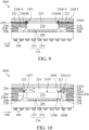
- FIG. 8 is a cross-sectional view of a semiconductor device 500H in accordance with some embodiments of the disclosure. Elements of the embodiments hereinafter, that are the same or similar as those previously described with reference to FIGS. 1 to 7 are not repeated for brevity.
- the difference between the semiconductor device 500H and the semiconductor device 500G at least includes a thermal dissipation structure 230H with a recess 230HR recessed from a bottom surface 230HB of the thermal dissipation structure 230H.
- the recess 230HR is positioned close to the edge of the semiconductor die 210.
- the gel 222 may fill the recess 230HR of thermal dissipation structure 230H.
- the recess 230HR of thermal dissipation structure 230H may provide an addition space for the gel 222 filling within, the seal quality of the semiconductor device 500H may be improved.
- the closed space of the semiconductor device 500H may be formed by the semiconductor die 210, the gel 222 and the thermal dissipation structure 230H.
- the closed space of the semiconductor device 500H may be formed by the top surface 210T of the semiconductor die 210, the gel 222 and the bottom surface of the thermal dissipation structure 230H.
- the lid 220F may be used to provide mechanical support for forming the closed space. Therefore, the liquid metal 224 can be stably sealed in the closed space to avoid spillage of the liquid metal.
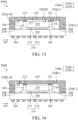
- FIG. 9 is a cross-sectional view of a semiconductor device 500I in accordance with some embodiments of the disclosure. Elements of the embodiments hereinafter, that are the same or similar as those previously described with reference to FIGS. 1 to 8 are not repeated for brevity.
- the difference between the semiconductor device 500I and the semiconductor device 500H at least includes that the semiconductor device 500I uses the gel 222 sealing the gap GP1 between the semiconductor die 210 and the extending portion 220F-E.
- the gel 222 fills recess 230HR of thermal dissipation structure 230H and the gap GP2 between the thermal dissipation structure 230A and a top surface 220FT of the extending portion 220F-E (it also serves as the top surface of the lid 220F).
- the lid 220F of the semiconductor device 500I may be attached to the thermal dissipation structure 230H only by the gel 222 (without using the adhesive 226 shown in FIG. 8 ).
- the closed space of the semiconductor device 5001 may be formed by the semiconductor die 210, the gel 222 and the thermal dissipation structure 230H.
- the closed space of the semiconductor device 500G may be formed by the top surface 210T of the semiconductor die 210, the gel 222 and the bottom surface of the thermal dissipation structure 230H.
- the lid 220F may be used to provide mechanical support for forming the closed space. Therefore, the liquid metal 224 can be stably sealed in the closed space to avoid spillage of the liquid metal.
- the semiconductor device may include a molding compound surrounding side surfaces of the semiconductor die 210.
- the molding compound may help to dissipate heat generated form the semiconductor die 210.
- the molding compound may provide an additional area for the dispensation of the gel 222.
- the thermal path area between the semiconductor die 210 and the liquid metal 224 may be increased, thereby improve heat dissipation efficiency from the semiconductor die 210 to the environment outside the semiconductor device.
- FIG. 10 is a cross-sectional view of a semiconductor device 500J in accordance with some embodiments of the disclosure. Elements of the embodiments hereinafter, that are the same or similar as those previously described with reference to FIGS. 1 to 9 are not repeated for brevity.
- the difference between the semiconductor device 500A and the semiconductor device 500J at least includes a molding compound 240 surrounding the semiconductor die 210.
- the bottom surface 220A-EB of the extending portion 220A-E may be higher than or flush with the top surface 210T of the semiconductor die 210 and a top surface 240T of the molding compound 240.
- the top surface 210T of the semiconductor die 210 may be flush with the top surface 240T of the molding compound 240.
- the bottom surface 240B of the molding compound 240 may be flush with bottom surface 240B of the semiconductor die 210.
- the gel 222 may be arranged on the edge of the top surface 240T of the molding compound 240 without extending to cover the top surface 210T of the semiconductor die 210. In other words, the entire top surface 210T of the semiconductor die 210 is exposed form the gel 222.
- the gel 222 may seals a gap GP3 between the molding compound 240 and the extending portion 220A-E. Therefore, the liquid metal 224 is in contact with the entire top surface 210T of the semiconductor die 210.
- the molded compound 240 may be formed of a nonconductive material, such as an epoxy, a resin, a moldable polymer, or the like.
- the molding compound 240 may be applied while substantially liquid, and then may be cured through a chemical reaction, such as in an epoxy or resin.
- the molding compound 240 may be an ultraviolet (UV) or thermally cured polymer applied as a gel or malleable solid capable of being disposed around the semiconductor die 210, and then may be cured using a UV or thermally curing process.
- UV ultraviolet
- thermally cured polymer applied as a gel or malleable solid capable of being disposed around the semiconductor die 210, and then may be cured using a UV or thermally curing process.
- the molding compound 240 may be cured with a mold.
- the gel 222 may be arranged on the molding compound 240 instead of the semiconductor die 210, so the thermal path between the semiconductor die 210 and the liquid metal 224 of the semiconductor device 500J is greater than that of the semiconductor device 500A. Therefore, the heat dissipation efficiency of the semiconductor device 500J is improved.
- the semiconductor device 500J shown in FIG. 10 may use the thermal dissipation structure 230D having the protrusion portion 230D-P ( FIG. 4 ) instead of the thermal dissipation structure 230A.
- the closed space of the semiconductor device 500J may be formed by the semiconductor die 210, the molded compound 240, the gel 222, the extending portion 220A-E of the lid 220A, the adhesive 226 and the thermal dissipation structure 230A, as shown in FIG. 10 .
- the gel 222 may completely cover the top surface 240T of the molded compound 240, and the closed space of the semiconductor device 500J may be formed by the semiconductor die 210, the gel 222, the extending portion 220A-E of the lid 220A, the adhesive 226 and the thermal dissipation structure 230A.
- the gel 222 may completely cover the side surface 220A-ES of the extending portion 220A-E of the lid 220A and the gel 222 may completely cover the top surface 240T of the molded compound 240, then the closed space of the semiconductor device 500J may be formed by the semiconductor die 210, the gel 222, the adhesive 226 and the thermal dissipation structure 230A.
- the gel 222 may be in contact with the bottom surface of the thermal dissipation structure 230A.
- the liquid metal 224 may not be in contact with the lid 220A and the adhesive 226, and the closed space may be formed by the semiconductor die 210, the gel 222 and the thermal dissipation structure 230A.
- the lid 220A may be used to provide mechanical support for forming the closed space. Therefore, the liquid metal 224 can be stably sealed in the closed space to avoid spillage of the liquid metal.
- FIG. 11 is a cross-sectional view of a semiconductor device 500K in accordance with some embodiments of the disclosure. Elements of the embodiments hereinafter, that are the same or similar as those previously described with reference to FIGS. 1 to 10 are not repeated for brevity.
- the difference between the semiconductor device 500J and the semiconductor device 500K at least includes the lid 220E with the extending portion 220E-E.
- the bottom surface 220E-EB of the extending portion 220E-E is lower than the top surface 210T of the semiconductor die 210 and the top surface 240T of the molding compound 240.
- the top surface 210T of the semiconductor die 210 (and the top surface 240T of the molding compound 240) may be positioned between the top surface 220ET and the bottom surface 220E-EB of the extending portion 220E-E. Therefore, the total height of the semiconductor device 500K can be reduced.
- the lower extending portion 220E-E may reduce a thickness T3 of the liquid metal 224 (e.g., the thickness T3 of the liquid metal 224 of the semiconductor device 500K is thinner than the thickness T1 of the liquid metal 224 of the semiconductor device 500J shown in FIG. 10 ) in order to improve heat dissipation efficiency and speed up heat dissipation.
- the semiconductor device 500K shown in FIG. 11 may use the thermal dissipation structure 230D having the protrusion portion 230D-P ( FIG. 4 ) instead of the thermal dissipation structure 230A.
- the closed space of the semiconductor device 500K may be formed by the semiconductor die 210, the molded compound 240, the gel 222, the extending portion 220E-E of the lid 220E, the adhesive 226 and the thermal dissipation structure 230A, as shown in FIG. 11 .
- the gel 222 may completely cover the side surface of the extending portion 220E-E of the lid 220E, and the closed space of the semiconductor device 500K may be formed by the semiconductor die 210, the molded compound 240, the gel 222, the adhesive 226 and the thermal dissipation structure 230A. In some embodiments, the gel 222 may be in contact with the bottom surface of the thermal dissipation structure 230A, then the closed space of the semiconductor device 500K may be formed by the semiconductor die 210, the molded compound 240, the gel 222 and the thermal dissipation structure 230A.
- the gel 222 may further completely cover the top surface 240T of the molded compound 240, as a result, the closed space may be formed by the semiconductor die 210, the gel 222 and the thermal dissipation structure 230A.
- the lid 220E may be used to provide mechanical support for forming the closed space. Therefore, the liquid metal 224 can be stably sealed in the closed space to avoid spillage of the liquid metal.
- FIG. 12 is a cross-sectional view of a semiconductor device 500M in accordance with some embodiments of the disclosure. Elements of the embodiments hereinafter, that are the same or similar as those previously described with reference to FIGS. 1 to 11 are not repeated for brevity.
- the difference between the semiconductor device 500K and the semiconductor device 500M at least includes that the extending portion 220F-E of the lid 220F of the semiconductor device 500M has a reduced height.
- the top surface 220FT of the extending portion 220F-E (it also serves as the top surface of the lid 220F) is flush with the top surface 210T of the semiconductor die 210 (and the top surface 240T of the molding compound 240).
- the bottom surface 220F-EB of the extending portion 220F-E may be positioned between the top surface 210T and the bottom surface 210B of the semiconductor die 210 (and the top surface 240T and the bottom surface 240B of the molding compound 240). Therefore, the total height of the semiconductor device 500M can be reduced.
- the gel 222 may be affixed to, and in contact with, the molding compound 240, the lid 220F and the thermal dissipation structure 230A without extending to cover the top surface 210T of the semiconductor die 210.
- the semiconductor device 500M including the lower extending portion 220F-E may reduce the thickness T4 of the liquid metal 224 (e.g., the thickness T4 of the liquid metal 224 of the semiconductor device 500M is thinner than the thickness T3 of the liquid metal 224 of the semiconductor device 500K shown in FIG. 11 ) in order to further improve heat dissipation efficiency and speed up heat dissipation. Therefore, the heat dissipation capability of the semiconductor device 500M can be further improved.
- the thickness T4 of the liquid metal 224 of the semiconductor device 500M is thinner than the thickness T3 of the liquid metal 224 of the semiconductor device 500K shown in FIG. 11
- the gel 222 may be in contact with the bottom surface of the thermal dissipation structure 230A, and the closed space of the semiconductor device 500M may be formed by the semiconductor die 210, the molded compound 240, the gel 222, and the thermal dissipation structure 230A.
- the gel 222 may further completely cover the top surface 240T of the molded compound 240, as a result, the closed space may be formed by the semiconductor die 210, the gel 222 and the thermal dissipation structure 230A.
- the lid 220F may be used to provide mechanical support for forming the closed space. Therefore, the liquid metal 224 can be stably sealed in the closed space to avoid spillage of the liquid metal.
- FIG. 13 is a cross-sectional view of a semiconductor device 500N in accordance with some embodiments of the disclosure. Elements of the embodiments hereinafter, that are the same or similar as those previously described with reference to FIGS. 1 to 12 are not repeated for brevity.
- the difference between the semiconductor device 500M and the semiconductor device 500N at least includes that the semiconductor device 500N uses the gel 222 sealing the gap GP3 between the molding compound 240 and the extending portion 220F-E and the gap GP2 between the thermal dissipation structure 230A and the top surface 220FT of the extending portion 220F-E (it also serves as the top surface of the lid 220F).
- the molding compound 240 and the lid 220F of the semiconductor device 500N may be attached to the thermal dissipation structure 230A only by the gel 222 (without using the adhesive 226 shown in FIG. 12 ).
- the closed space of the semiconductor device 500N may be formed by the semiconductor die 210, the molded compound 240, the gel 222, and the thermal dissipation structure 230A, as shown in FIG. 13 .
- the gel 222 may further completely cover the top surface 240T of the molded compound 240, as a result, the closed space may be formed by the semiconductor die 210, the gel 222 and the thermal dissipation structure 230A.
- the lid 220F may be used to provide mechanical support for forming the closed space. Therefore, the liquid metal 224 can be stably sealed in the closed space to avoid spillage of the liquid metal.
- the lid of the semiconductor device may be an integrated structure fully covering the top surface and side surfaces of the semiconductor die.
- the liquid metal is disposed between the semiconductor die and the lid and surrounded by the gel (or the adhesive).
- FIG. 14 is a cross-sectional view of a semiconductor device 500P in accordance with some embodiments of the disclosure. Elements of the embodiments hereinafter, that are the same or similar as those previously described with reference to FIGS. 1 to 13 are not repeated for brevity.
- the semiconductor device 500P includes the substrate 200, the conductive structures 204 and 216, the adhesive 208, the semiconductor die 210, the molding compound 240, the liquid metal 224, a lid 220P and a gel 322.
- the difference between the semiconductor device 500J and the semiconductor device 500P at least includes that the semiconductor device 500P is fabricated without using the thermal dissipation structure.
- the lid 220P of the semiconductor device 500P is disposed on the substrate 200 and covers the semiconductor die 210 and the molding compound 240.
- the lid 220P may be an integrated structure without any through hole located at the lid 220P.
- the lid 220P includes an upper portion 220P-1 and a lower portion 220P-2 connected to the upper portion 220P-1.
- the upper portion 220P-1 may laterally extend over the semiconductor die 210 to cover the entire top surface 210T of the semiconductor die 210 and the entire top surface 240T of the molding compound 240.
- the lower portion 220P-2 may vertically extend to cover the entire side surface 2105 of the semiconductor die 210 and an entire side surface 2405 of the molding compound 240.
- the lid 220P has an inverted-U shape in the cross-sectional view as shown in FIG. 14 .
- the substrate 200 and the lid 220P connected to each other by the adhesive 208 may collectively form a closed space to accommodate the semiconductor die 210 and the molding compound 240.
- the gel 322 is disposed on the top surface 240T of the molding compound 240.
- the gel 322 is arranged between the molding compound 240 and the lid 220P without extending to cover the top surface 210T of the semiconductor die 210.
- the gel 322 is in contact with the top surface 240T of the molding compound 240 and a bottom surface 220P-1B of the upper portion 220P-1 of the lid 220P.
- the gel 222, 322 and the adhesives 208, 226 may comprise the same or similar materials.
- the lid 220P has a top surface 220PT opposite to the bottom surface 220P-1B, the top surface 220PT of the lid 220P may be a flat surface and the lid 220P has no opening on the top surface 220PT.
- the lid 220P has at least one protrusion portion 220P-P protruding from the bottom surface 220P-1B of the upper portion 220P-1 of the lid 220P.
- the bottom surface 220P-1B of the upper portion 220P-1 of the lid 220P is not a flat surface.
- the at least one protrusion portion 220P-P may extend towards the top surface 210T of the semiconductor die 210 and surrounded by the gel 322.
- the gel 322 may be in contact with side surfaces of the protrusion portion 220P-P.
- the liquid metal 224 is arranged between and in contact with the entire top surface 210T of the semiconductor die 210 and the lid 220P.
- the liquid metal 224 may be surrounded by the gel 322.
- the semiconductor die 210 and the lid 220P sealed each other by the gel 322 may collectively form a closed space to accommodate the liquid metal 224 filling within, thereby providing a heat dissipating path with low-thermal resistance.
- FIG. 14 the liquid metal 224 is arranged between and in contact with the entire top surface 210T of the semiconductor die 210 and the lid 220P.
- the liquid metal 224 may be surrounded by the gel 322.
- the semiconductor die 210 and the lid 220P sealed each other by the gel 322 may collectively form a closed space to accommodate the liquid metal 224 filling within, thereby providing a heat dissipating path with low-thermal resistance.
- gel 322 may completely cover the top surface 240T of the molded compound 240, as a result, the semiconductor die 210, the lid 220P and the gel 322 form the closed space to accommodate the liquid metal 224, thereby providing a heat dissipating path with low-thermal resistance.
- the closed space of the semiconductor device 500P may be formed by the semiconductor die 210, the gel 322 and the at least one protrusion portion 220P-P of the integrated lid 220P.
- gel 322 may partly cover the top surface 240T of the molded compound 240, then the closed space of the semiconductor device 500P may be formed by the semiconductor die 210, the molded compound 240, the gel 322 and the lid 220P. Therefore, the liquid metal 224 can be stably sealed in the closed space to avoid spillage of the liquid metal.
- the protrusion portion 220P-P of the integrated lid 220P may reduce a thickness T5 of the liquid metal 224 (e.g., the thickness T5 of the liquid metal 224 of the semiconductor device 500P is thinner than a thickness T1 of the liquid metal 224 of the semiconductor device 500J shown in FIG. 10 ) in order to improve heat dissipation efficiency and speed up heat dissipation.
- the thickness T5 of the liquid metal 224 may be thinner than a thickness T6 of the gel 322. Therefore, the heat dissipation capability of the semiconductor device 500P can be further improved.
- FIG. 15 is a cross-sectional view of a semiconductor device 500Q in accordance with some embodiments of the disclosure. Elements of the embodiments hereinafter, that are the same or similar as those previously described with reference to FIGS. 1 to 14 are not repeated for brevity.
- the difference between the semiconductor device 500P and the semiconductor device 500Q at least includes that the semiconductor device 500Q includes a lid 220Q.
- the lid 220Q includes an upper portion 220Q-1 and a lower portion 220Q-2 connected to the upper portion 220Q-1.
- the lid 220Q may have at least one recess 220QR on a bottom surface 220Q-1B of an upper portion 220Q-1 of the lid 220Q.
- the bottom surface 220Q-1B of the upper portion 220Q-1 of the lid 220Q is not a flat surface.
- the at least one recess 220QR of the lid 220Q provides an additional space to accommodate the liquid metal 224.
- a thickness T7 of the liquid metal 224 may be greater than a thickness T8 of the gel 322.
- the total height of the semiconductor device 500Q can be further reduced.
- the gel 322 may completely cover the top surface 240T of the molded compound 240, as a result, the closed space of the semiconductor device 500Q may be formed by the semiconductor die 210, the gel 322 and the lid 220Q.
- the closed space of the semiconductor device 500Q may be formed by the semiconductor die 210, the gel 322 and the at least one recess 220QR of the lid 220Q.
- the gel 322 may partly cover the top surface 240T of the molded compound 240, then the closed space of the semiconductor device 500Q may be formed by the semiconductor die 210, the molded compound 240, the gel 322 and the lid 220Q. Therefore, the liquid metal 224 can be stably sealed in the closed space to avoid spillage of the liquid metal.
- FIG. 16 is a cross-sectional view of a semiconductor device 500R in accordance with some embodiments of the disclosure. Elements of the embodiments hereinafter, that are the same or similar as those previously described with reference to FIGS. 1 to 15 are not repeated for brevity.
- the difference between the semiconductor device 500P and the semiconductor device 500R at least includes a lid 220R with an upper portion 220R-1 and a lower portion 220R-2 connected to the upper portion 220R-1.
- the upper portion 220R-1 of the semiconductor device 500R has a uniform thickness T9 (the upper portion 220R-1 is formed without protrusion portions or recesses).
- the liquid metal 224 and the gel 322 may have the same thickness T10.
- the gel 322 may completely cover the top surface 240T of the molded compound 240, as a result, the closed space of the semiconductor device 500R may be formed by the semiconductor die 210, the gel 322 and the lid 220R.
- the closed space of the semiconductor device 500R may be formed by the semiconductor die 210, the gel 322 and the bottom surface 220R-1B of an upper portion 220R-1 of the lid 220R.
- the gel 322 may partly cover the top surface 240T of the molded compound 240, then the closed space of the semiconductor device 500R may be formed by the semiconductor die 210, the molded compound 240, the gel 322 and the lid 220R. Therefore, the liquid metal 224 can be stably sealed in the closed space to avoid spillage of the liquid metal.
- Embodiments provide a semiconductor device.
- the semiconductor device may include a substrate, a semiconductor die, a lid, a liquid metal, a gel and a thermal dissipation structure.
- the lid and the thermal dissipation structure connected to each other may collectively form a composite lid.
- the lid may include an extending portion extending towards the semiconductor die.
- the lid may have an opening to expose the semiconductor die.
- the gel is disposed between the semiconductor die and the lid.
- the thermal dissipation structure is disposed on the lid and covers the opening.
- the liquid metal disposed on the semiconductor die and in the opening.
- the thermal dissipation structure covers the liquid metal.
- the semiconductor die, extending portion of the lid and the thermal dissipation structure may collectively form a closed space to accommodate the liquid metal filling within, thereby providing a heat dissipating path with low-thermal resistance.
- the liquid metal is stably sealed in the closed space, when the semiconductor device is shipped, the area of the top surface of the semiconductor die covered by the liquid metal may keep the same. Being stably sealed in the closed space can also prevent the liquid metal from leaking to outside.
- the thermal dissipation structure may have the protrusion portion protruding from the top surface of the thermal dissipation structure to increase the surface area of the thermal dissipation structure, thereby improving heat dissipation efficiency.
- thermal dissipation structure may have protrusion portion protruding from the bottom surface of the thermal dissipation structure to reduce the thickness of the liquid metal in order to improve heat dissipation efficiency and speed up heat dissipation.
- the thermal dissipation structure may have the recess providing the addition space for the gel filling within.
- the lid having the opening to expose the semiconductor die may have a reduced height in order to reduce the total height of the semiconductor device.
- the semiconductor device includes the molding compound surrounding the semiconductor die. The molding compound may help to dissipate heat generated form the semiconductor die. In addition, the molding compound may provide an additional area for the dispensation of the gel. The thermal path area between the semiconductor die and the liquid metal may be increased.
- the lid of the semiconductor device may have an integrated structure without openings (or the through holes). The lid may fully cover the top surface and side surfaces of the semiconductor die.
- the semiconductor die and the lid connected each other may collectively form a closed space to accommodate the liquid metal filling within.
- the liquid metal may be disposed between the entire top surface of the semiconductor die and the lid and surrounded by the gel (or the adhesive).
- the thickness of the liquid metal and the total height of the semiconductor device may be further reduced while the semiconductor device has a recess on the bottom surface of the lid.
Landscapes
- Cooling Or The Like Of Semiconductors Or Solid State Devices (AREA)
Abstract
Description
- This application claims the benefit of
U.S. Provisional Application No. 63/491,784, filed on March 23, 2023 - The present disclosure relates to a semiconductor device and, in particular, to a semiconductor device including a liquid metal.
- Conventional semiconductor device includes a substrate and an electronic component disposed on the substrate. However, the electronic component inevitably generates heat during operation. Thus, how to dissipate the heat from the electronic component has become a prominent task for the industry.
- An embodiment of the present disclosure provides a semiconductor device. The semiconductor device includes a substrate, a semiconductor die, a lid, a liquid metal, a gel and a thermal dissipation structure. The semiconductor die is disposed on the substrate. The lid is disposed on the substrate and covers the semiconductor die. The lid has an opening to expose the semiconductor die. The liquid metal is disposed on the semiconductor die. The gel is disposed between the semiconductor die and the lid. The thermal dissipation structure is disposed on the lid and covers the liquid metal. The semiconductor die, the gel and the thermal dissipation structure form a closed space for accommodating the liquid metal.
- In some embodiments, the lid comprises an extending portion extending towards the semiconductor die, and the gel is in contact with the extending portion of the lid to seal a gap between the semiconductor die and the extending portion. In some embodiments, a bottom surface of the extending portion is higher than or flush with a top surface of the semiconductor die. In some embodiments, a top surface of the thermal dissipation structure is flush with a top surface of the lid. In some embodiments, the thermal dissipation structure has a protrusion portion protruding from a bottom surface and/or a top surface of the thermal dissipation structure. In some embodiments, a bottom surface of the extending portion is lower than a top surface of the semiconductor die; and/or a top surface of the extending portion is flush with the top surface of the semiconductor die. In some embodiments, the thermal dissipation structure comprises a metal plate or a heat sink. In some embodiments, the gel is affixed to the thermal dissipation structure. In some embodiments, the thermal dissipation structure covers a top surface of the extending portion, and the gel fills a gap between the thermal dissipation structure and the top surface of the extending portion. In some embodiments, the gel fills a recess of thermal dissipation structure, wherein the recess is recessed from a bottom surface of the thermal dissipation structure. In some embodiments, the gel is arranged on an edge of a top surface of the semiconductor die. In some embodiments, the semiconductor device further includes conductive structures disposed between the substrate and the semiconductor die. In some embodiments, the semiconductor device further includes an underfill arranged between the substrate and the semiconductor die and surrounding the conductive elements. In some embodiments, the lid is arranged on the substrate by an adhesive. In some embodiments, the thermal dissipation structure is arranged on the lid by an adhesive. In some embodiments, the semiconductor device further includes a molding compound surrounding the semiconductor die. The gel is arranged on an edge of a top surface of the molding compound. In some embodiments, the liquid metal is in contact with an entire top surface of the semiconductor die. In some embodiments, a bottom surface of the extending portion is higher than or flush with a top surface of the semiconductor die; or the bottom surface of the extending portion is lower than the top surface of the semiconductor die. In some embodiments, a top surface of the extending portion is flush with a top surface of the semiconductor die.
- An embodiment of the present disclosure provides a semiconductor device. The semiconductor device includes a substrate, a semiconductor die, a molding compound, a lid, a gel and a liquid metal. The semiconductor die is disposed on the substrate. The lid is disposed on the substrate and covers the semiconductor die and the molding compound. The gel is arranged between the molding compound and the lid. The liquid metal is arranged between an entire top surface of the semiconductor die and the lid. The semiconductor die, the lid, the gel and the thermal dissipation structure form a closed space for accommodating the liquid metal.
- In some embodiments, the lid has a recess on a bottom surface of the lid; or the lid has a protrusion portion protruding from the bottom surface of the lid. In some embodiments, the lid is an integrated structure.
- The present disclosure can be more fully understood by reading the subsequent detailed description and examples with references made to the accompanying drawings, wherein:
FIGS. 1, 2 ,3, 4 ,5, 6 ,7, 8 ,9, 10 ,11, 12 ,13, 14 ,15 and 16 are cross-sectional views of a semiconductor device in accordance with some embodiments of the disclosure. - The following description is made for the purpose of illustrating the general principles of the disclosure and should not be taken in a limiting sense. The scope of the disclosure is best determined by reference to the appended claims.
- The inventive concept is described fully hereinafter with reference to the accompanying drawings, in which exemplary embodiments of the inventive concept are shown. The advantages and features of the inventive concept and methods of achieving them will be apparent from the following exemplary embodiments that will be described in more detail with reference to the accompanying drawings. It should be noted, however, that the inventive concept is not limited to the following exemplary embodiments, and may be implemented in various forms. Accordingly, the exemplary embodiments are provided only to disclose the inventive concept and let those skilled in the art know the category of the inventive concept. Also, the drawings as illustrated are only schematic and are nonlimiting. In the drawings, the size of some of the elements may be exaggerated for illustrative purposes and not drawn to scale. The dimensions and the relative dimensions do not correspond to actual dimensions in the practice of the disclosure.
- With the increased usage of the semiconductor devices, satisfying power needs has become a priority. When the device power is getting higher, the thermal dissipation of the semiconductor device is highly concerned to avoid performance degradation of the semiconductor device induced by the high temperature. The conventional thermal interface material 1 (TIM 1) dispensed between a flip-chip semiconductor die and a heat-spreading lid has poor heat dissipation capability for the semiconductor device in high-power operation. Therefore, liquid metals (LMs) with high thermal conductivity may act as an excellent solution to high thermal problem. However, the liquid metal used in TIM1 applications may easily spread to undesired spaces and further cause coverage issue and circuit short problem while touching the substrate or electronic components (such as semiconductor dies/capacitors/resistors/inductors). When the temperature rises or the semiconductor device isn't fixed horizontally, the liquid metal will flow outside, and further pollute the substrate or other components (such as semiconductor dies/capacitors/resistors/inductors). Thus, a novel semiconductor device that includes a liquid metal is desirable.
-
FIG. 1 is a cross-sectional view of asemiconductor device 500A in accordance with some embodiments of the disclosure. In some embodiments, thesemiconductor device 500A is a portion of mobile phones, personal digital assistants (PDA), digital cameras, and servers, etc.. Thesemiconductor device 500A is capable of applying to (or disposed on) a package requiring high-power operation, such as flip chip ball grid array (FCBGA), land grid array (LGA), fan-out package, three-dimensional (3D) integrated circuit (IC) package, etc.. As show inFIG. 1 , thesemiconductor device 500A includes asubstrate 200, asemiconductor die 210, alid 220A, aliquid metal 224, agel 222 and athermal dissipation structure 230A. - The
substrate 200 can be a single layer or a multilayer structure. In some embodiments, thesubstrate 200 is, for example, a printed circuit board (PCB), an interposer, a package substrate, another semiconductor device or a semiconductor package. In some embodiments, thesubstrate 200 may be formed of dielectric materials (e.g., polypropylene (PP), epoxy, polyimide, or other applicable resin materials) or semiconductor materials. Thesubstrate 200 has atop surface 200T and abottom surface 200B opposite thetop surface 200T. Thesubstrate 200 is provided for the semiconductor die 210 disposed on thetop surface 200T. A plurality of conductive traces (not shown), conductive vias and/or conductive pads (not shown) are disposed in thesubstrate 200. The conductive traces may be electrically connected to the corresponding conductive vias and conductive pads. The conductive pads and/or the conductive traces are exposed to openings of solder mask layers (not shown) disposed close to thetop surface 200T and thebottom surface 200B. In one embodiment, the conductive traces may comprise signal trace segments or ground trace segments, which are used for the input/output (I/O) connections of the semiconductor die 210. Also, the conductive pads are disposed on thetop surface 200T of thesubstrate 200, connected to different terminals of the conductive traces. The conductive pads are used for the semiconductor die 210 that is mounted directly on them. - The
semiconductor device 500A further includesconductive structures 204 disposed on thebottom surface 200B ofsubstrate 200 away from the semiconductor die 210 and in contact with the corresponding the conductive pads (not shown) of thesubstrate 200. In some embodiments, theconductive structures 204 includes a conductive ball structure such as a solder ball, copper-core solder ball, a conductive bump structure such as a copper bump or a solder bump structure, or a conductive pillar structure such as a copper pillar structure. - As shown in
FIG. 1 , the semiconductor die 210 is flipped to be disposed on thesubstrate 200 opposite theconductive structures 204 by a bonding process. The semiconductor die 210 is mounted on thesubstrate 200 usingconductive structures 216. In addition, the semiconductor die 210 is electrically connected to theconductive structures 204 by thesubstrate 200. The semiconductor die 210 is, for example, a fan-out semiconductor die, such a central processing unit (CPU), a graphic processing unit (GPU), a dynamic random access memory (DRAM) controller or any combination thereof. In some embodiments, the semiconductor die 210 is fabricated by a flip-chip technology. - In some embodiments, the
conductive structures 216 are electrically connected to the conductive pads (including conductive traces) of thesubstrate 200. In some embodiments, theconductive structures 216 include a conductive ball structure such as a solder ball, copper-core solder ball, a conductive bump structure such as a copper bump or a solder bump structure, or a conductive pillar structure such as a copper pillar structure. For example, one of theconductive structures 216 may include aconductive pillar structure 212 and aconductive bump structure 214. - As shown in
FIG. 1 , thesemiconductor device 500A further includes anunderfill 218 arranged between thesubstrate 200 and the semiconductor die 210. Theunderfill 218 surrounds theconductive elements 216. Theunderfill 218 fills the gap (not shown) between thesubstrate 200 and the semiconductor die 210. Theunderfill 218 covers abottom surface 210B of the semiconductor die 210 and thetop surface 200T ofsubstrate 200. Theunderfill 218 is also in contact with thebottom surface 210B of the semiconductor die 210 and thetop surface 200T ofsubstrate 200. Theunderfill 218 may help to dissipate heat generated from the semiconductor die 210 and to reduce the thermal resistance from the semiconductor die 210 to thesubstrate 200. Theunderfill 218 surrounds and covers side surfaces 2105 of the semiconductor die 210. Theunderfill 218 may be in contact with the side surfaces 2105 of the semiconductor die 210. Theunderfill 218 may help stabilize the semiconductor die 210. - As shown in
FIG. 1 , thelid 220A is disposed on thesubstrate 200. In addition, thelid 220A is disposed so that it surrounds and covers side surfaces 2105 of the semiconductor die 210. Thelid 220A may also surround and cover theunderfill 218. Thelid 220A and theunderfill 218 may not be in contact with each other. In some embodiments, there is a space between thelid 220A and theunderfill 218. In some embodiments, thelid 220A includes an extendingportion 220A-E extending towards the semiconductor die 210. The extendingportion 220A-E may also cover the space between thelid 220A and theunderfill 218. The extendingportion 220A-E has an opening 221 (or a through hole) directly above the semiconductor die 210 to expose an entiretop surface 210T of the semiconductor die 210. The extendingportion 220A-E has a top surface 220AT and abottom surface 220A-EB. The top surface 220AT may also serve as the top surface of thelid 220A. In some embodiments, thebottom surface 220A-EB of the extendingportion 220A-E is higher than or flush with thetop surface 210T of the semiconductor die 210. In some embodiments, thelid 220A may be made by a metal material, such as copper, aluminum, iron or a combination thereof. In some embodiments, thelid 220A may be made by a non-metal material, such as a ceramic material, a polymer material or another applicable non-metal material. Thelid 220A could conduct heat and increase strength of thesemiconductor device 500A for reducing warpage. - As shown in
FIG. 1 , thesemiconductor device 500A further includes an adhesive 208 disposed between thelid 220A and the on thetop surface 200T of thesubstrate 200, so that thelid 220A is arranged on thetop surface 200T of thesubstrate 200. - As shown in
FIG. 1 , thegel 222 is disposed between the semiconductor die 210 and thelid 220A. Thegel 222 may be arranged on an edge of thetop surface 210T of the semiconductor die 210. In addition, thegel 222 may be in contact with aside surface 220A-ES of the extendingportion 220A-E of thelid 220A to seal a gap GP1 between the semiconductor die 210 and the extendingportion 220A-E. In some embodiments, thegel 222 covers and is contact with a portion of thetop surface 210T of the semiconductor die 210. In some embodiments, thegel 222 includes a silicone based material, an epoxy based material, an acrylic based material, a silver paste, etc.. - As shown in
FIG. 1 , theliquid metal 224 is disposed on the semiconductor die 210 and in contact with thetop surface 210T of the semiconductor die 210. In some embodiments, the semiconductor die 210, thegel 222, the extendingportion 220A-E of thelid 220A and thethermal dissipation structure 230A may collectively form a closed space to accommodate theliquid metal 224. In some embodiments, theliquid metal 224 may substantially fill up the closed space. In terms of the property, theliquid metal 224 may have melting point ranging between 25° C. to 70° C., lower or higher. The thermal conductivity of theliquid metal 224 is higher than that of the conventional thermal interface material (TIM). Generally, the TIM has thermal conductivity ranging between 2 W/m-K to 10 W/m-K. In some embodiments, theliquid metal 224 includes a gallium alloys or a compound of gallium, indium (e.g., eutectic gallium indium (EGaIn) (75% gallium and 25% indium) and Galinstan (GaInSn) (68.5% gallium, 21.5% indium and 10% tin)). - As shown in
FIG. 1 , thethermal dissipation structure 230A is disposed on thelid 220A. Thethermal dissipation structure 230A may be arranged on the top surface 220AT of thelid 220A by an adhesive 226. In addition, thethermal dissipation structure 230A may laterally (along a direction 100) extend over the top surface 220AT of thelid 220A to cover theopening 221. The plate-shapedthermal dissipation structure 230A may have a uniform thickness. In some embodiments, thethermal dissipation structure 230A and thelid 220A may comprise the same or similar materials. In some embodiments, thethermal dissipation structure 230A comprises a metal plate, ceramic plate, or a heat sink. In some embodiments, a bottom surface of thethermal dissipation structure 230A is a flat surface. In some embodiments, thegel 222 and theadhesives thermal dissipation structure 230A and thelid 220A are separate structures, not an integrated structure. - In some embodiments, the
lid 220A having theopening 221 is used in combination with thethermal dissipation structure 230A, and thegel 222 is used to seal the gap between the semiconductor die 210 and thelid 220A. Thelid 220A and thethermal dissipation structure 230A may collectively form a composite lid. In addition, as the gap between the semiconductor die 210 and the extendingportion 220A-E of thelid 220A is sealed by thegel 222 and the adhesive 226 is disposed between thelid 220A and thethermal dissipation structure 230A, as a result, the semiconductor die 210, the extendingportion 220A-E of thelid 220A and thethermal dissipation structure 230A may collectively form the closed space to accommodate theliquid metal 224 filling within, thereby providing a heat dissipating path with low-thermal resistance. In some embodiments, the semiconductor die 210, thegel 222, the extendingportion 220A-E of thelid 220A, the adhesive 226 and thethermal dissipation structure 230A may collectively form the closed space. In some embodiments, thetop surface 210T of the semiconductor die 210, thegel 222, the extendingportion 220A-E of thelid 220A, the adhesive 226 and the bottom surface of thethermal dissipation structure 230A may collectively form the closed space. In addition, as theliquid metal 224 is stably sealed in the closed space, when thesemiconductor device 500A is shipped, the area of thetop surface 210T of the semiconductor die 210 covered by theliquid metal 224 may keep the same. Being stably sealed in the closed space can also prevent theliquid metal 224 from leaking to outside. Therefore, the circuit short problem is eliminated, and the heat dissipation capability of the semiconductor device can be further improved. - In some embodiments, the
gel 222 may completely cover theside surface 220A-ES of the extendingportion 220A-E of thelid 220A, and the adhesive 226 may completely cover the top surface 220AT of thelid 220A. In such an embodiment, the closed space may be formed by the semiconductor die 210, thegel 222, the adhesive 226 and thethermal dissipation structure 230A. In more detail, the closed space may be formed by thetop surface 210T of the semiconductor die 210, thegel 222, the adhesive 226 and the bottom surface of thethermal dissipation structure 230A. In some embodiments, thegel 222 may be in contact with the adhesive 226. In some embodiments, thegel 222 may be in contact with the bottom surface of thethermal dissipation structure 230A. As a result, theliquid metal 224 may not be in contact with thelid 220A and the adhesive 226. In such an embodiment, the closed space may be formed by the semiconductor die 210, thegel 222 and thethermal dissipation structure 230A. In more detail, the closed space may be formed by thetop surface 210T of the semiconductor die 210, thegel 222 and the bottom surface of thethermal dissipation structure 230A. According to some embodiments, thelid 220A may be used to provide mechanical support for forming the closed space. Therefore, theliquid metal 224 can be stably sealed in the closed space to avoid spillage of the liquid metal. -
FIG. 2 is a cross-sectional view of asemiconductor device 500B in accordance with some embodiments of the disclosure. Elements of the embodiments hereinafter, that are the same or similar as those previously described with reference toFIG. 1 are not repeated for brevity. The difference between thesemiconductor device 500A and thesemiconductor device 500B at least includes athermal dissipation structure 230B with at least oneprotrusion portion 230B-P. Theprotrusion portion 230B-P extends upwards form from a top surface 230BT of thethermal dissipation structure 230B . In some embodiments, the fin-shapedprotrusion portion 230B-P may increase the surface area of thethermal dissipation structure 230B. Therefore, the heat dissipation capability of thesemiconductor device 500B can be further improved. -
FIG. 3 is a cross-sectional view of asemiconductor device 500C in accordance with some embodiments of the disclosure. Elements of the embodiments hereinafter, that are the same or similar as those previously described with reference toFIGS. 1 and 2 are not repeated for brevity. The difference between thesemiconductor device 500A and thesemiconductor device 500C at least includes athermal dissipation structure 230C disposed on alid 220C. Thethermal dissipation structure 230C is mounted on an extendingportion 220C-E of thelid 220C by an adhesive 226C. In addition, thethermal dissipation structure 230C and the adhesive 226C are surrounded by thelid 220C. Side surfaces (not shown) of thethermal dissipation structure 230C is connected to side surfaces 220CS of thelid 220C which is above the extendingportion 220C-E. In some embodiments, a top surface 230CT of thethermal dissipation structure 230C is flush with a top surface 220CT of thelid 220C. The top surface 230CT of thethermal dissipation structure 230C may be a flat surface and thethermal dissipation structure 230C has no opening on the top surface 230CT. It is convenient for manufacturing and subsequent installation of thesemiconductor device 500C. -
FIG. 4 is a cross-sectional view of asemiconductor device 500D in accordance with some embodiments of the disclosure. Elements of the embodiments hereinafter, that are the same or similar as those previously described with reference toFIGS. 1 to 3 are not repeated for brevity. The difference between thesemiconductor device 500A and thesemiconductor device 500D at least includes athermal dissipation structure 230D with at least oneprotrusion portion 230D-P. The at least oneprotrusion portion 230D-P is facing the opening. Theprotrusion portion 230D-P protrudes from a bottom surface 230DB of thethermal dissipation structure 230D and extends towards thetop surface 210T of the semiconductor die 210. In other words, the bottom surface of thethermal dissipation structure 230D is not a flat surface. A top surface 230DT of thethermal dissipation structure 230D may be a flat surface and thethermal dissipation structure 230D has no opening on the top surface 230DT. In some embodiments, theprotrusion portion 230D-P may reduce a thickness T2 of the liquid metal 224 (e.g., the thickness T2 of theliquid metal 224 of thesemiconductor device 500D is thinner than a thickness T1 of theliquid metal 224 of thesemiconductor device 500A shown inFIG. 1 ) in order to improve heat dissipation efficiency and speed up heat dissipation. Therefore, the heat dissipation capability of thesemiconductor device 500B can be further improved. -
FIG. 5 is a cross-sectional view of asemiconductor device 500E in accordance with some embodiments of the disclosure. Elements of the embodiments hereinafter, that are the same or similar as those previously described with reference toFIGS. 1 to 4 are not repeated for brevity. The difference between thesemiconductor device 500A and thesemiconductor device 500E at least includes alid 220E with an extendingportion 220E-E. In some embodiments, abottom surface 220E-EB of the extendingportion 220E-E is lower than thetop surface 210T of the semiconductor die 210. In addition, thetop surface 210T of the semiconductor die 210 may be lower than a top surface 220ET of the extendingportion 220E-E. Therefore, the total height of thesemiconductor device 500E can be reduced. In some embodiments, the lower extendingportion 220E-E may reduce a thickness T3 of the liquid metal 224 (e.g., the thickness T3 of theliquid metal 224 of thesemiconductor device 500E is thinner than a thickness T1 of theliquid metal 224 of thesemiconductor device 500A shown inFIG. 1 ) in order to improve heat dissipation efficiency and speed up heat dissipation. Therefore, the heat dissipation capability of thesemiconductor device 500E can be further improved. In some embodiments, thesemiconductor device 500E shown inFIG. 5 may use thethermal dissipation structure 230D having theprotrusion portion 230D-P (FIG. 4 ) instead of thethermal dissipation structure 230A. In some embodiments, the closed space of thesemiconductor device 500E may be formed by the semiconductor die 210, the extendingportion 220E-E of thelid 220E, thegel 222, the adhesive 226 and thethermal dissipation structure 230A. In some embodiments, when thegel 222 completely cover the side surface of the extendingportion 220E-E of thelid 220E and the adhesive 226 completely cover the top surface 220ET of thelid 220E, the closed space of thesemiconductor device 500E may be formed by the semiconductor die 210, thegel 222, the adhesive 226 and thethermal dissipation structure 230A. In some embodiments, thegel 222 may be in contact with the bottom surface of thethermal dissipation structure 230A, and the closed space of thesemiconductor device 500E may be formed by the semiconductor die 210, thegel 222 and thethermal dissipation structure 230A. According to some embodiments, thelid 220E may be used to provide mechanical support for forming the closed space. Therefore, theliquid metal 224 can be stably sealed in the closed space to avoid spillage of the liquid metal. -
FIG. 6 is a cross-sectional view of asemiconductor device 500F in accordance with some embodiments of the disclosure. Elements of the embodiments hereinafter, that are the same or similar as those previously described with reference toFIGS. 1 to 5 are not repeated for brevity. The difference between thesemiconductor device 500E and thesemiconductor device 500F at least includes alid 220F with an extendingportion 220F-E. In some embodiments, a top surface 220FT of the extendingportion 220F-E (it also serves as the top surface of thelid 220F) is flush with the top 210T of the semiconductor die 210. In addition, abottom surface 220F-EB of the extendingportion 220F-E may be lower than thetop surface 210T of the semiconductor die 210. Furthermore, thegel 222 may be affixed to, and in contact with, the semiconductor die 210, thelid 220F and thethermal dissipation structure 230A. Therefore, the total height of thesemiconductor device 500F can be reduced. Compared with thesemiconductor device 500E, thesemiconductor device 500F including the lower extendingportion 220F-E may reduce a thickness T4 of the liquid metal 224 (e.g., the thickness T4 of theliquid metal 224 of thesemiconductor device 500E is thinner than a thickness T3 of theliquid metal 224 of thesemiconductor device 500E shown inFIG. 5 ) in order to further improve heat dissipation efficiency and speed up heat dissipation. Therefore, the heat dissipation capability of thesemiconductor device 500F can be further improved. In some embodiments, thegel 222 seals the gap between the semiconductor die 210 and the extendingportion 220F-E, and thegel 222 may be in contact with the bottom surface of thethermal dissipation structure 230A. As a result, the closed space of thesemiconductor device 500F may be formed by the semiconductor die 210, thegel 222 and thethermal dissipation structure 230A. In some embodiments, the closed space may be formed by thetop surface 210T of the semiconductor die 210, thegel 222 and the bottom surface of thethermal dissipation structure 230A. According to some embodiments, thelid 220F may be used to provide mechanical support for forming the closed space. Therefore, theliquid metal 224 can be stably sealed in the closed space to avoid spillage of the liquid metal. -
FIG. 7 is a cross-sectional view of asemiconductor device 500G in accordance with some embodiments of the disclosure. Elements of the embodiments hereinafter, that are the same or similar as those previously described with reference toFIGS. 1 to 6 are not repeated for brevity. The difference between thesemiconductor device 500F and thesemiconductor device 500G at least includes that thesemiconductor device 500G uses thegel 222 sealing the gap GP1 between the semiconductor die 210 and the extendingportion 220F-E. In addition, thegel 222 fills a gap GP2 between thethermal dissipation structure 230A and a top surface 220FT of the extendingportion 220F-E (it also serves as the top surface of thelid 220F). Compared with thesemiconductor device 500F, thelid 220F of thesemiconductor device 500G may be attached to thethermal dissipation structure 230A only by the gel 222 (without using the adhesive 226 shown inFIG. 6 ). In some embodiments, the closed space of thesemiconductor device 500G may be formed by the semiconductor die 210, thegel 222 and thethermal dissipation structure 230A. In some embodiments, the closed space of thesemiconductor device 500G may be formed by thetop surface 210T of the semiconductor die 210, thegel 222 and the bottom surface of thethermal dissipation structure 230A. According to some embodiments, thelid 220F may be used to provide mechanical support for forming the closed space. Therefore, theliquid metal 224 can be stably sealed in the closed space to avoid spillage of the liquid metal. -
FIG. 8 is a cross-sectional view of asemiconductor device 500H in accordance with some embodiments of the disclosure. Elements of the embodiments hereinafter, that are the same or similar as those previously described with reference toFIGS. 1 to 7 are not repeated for brevity. The difference between thesemiconductor device 500H and thesemiconductor device 500G at least includes athermal dissipation structure 230H with a recess 230HR recessed from a bottom surface 230HB of thethermal dissipation structure 230H. The recess 230HR is positioned close to the edge of the semiconductor die 210. Thegel 222 may fill the recess 230HR ofthermal dissipation structure 230H. In some embodiments, the recess 230HR ofthermal dissipation structure 230H may provide an addition space for thegel 222 filling within, the seal quality of thesemiconductor device 500H may be improved. In some embodiments, the closed space of thesemiconductor device 500H may be formed by the semiconductor die 210, thegel 222 and thethermal dissipation structure 230H. In some embodiments, the closed space of thesemiconductor device 500H may be formed by thetop surface 210T of the semiconductor die 210, thegel 222 and the bottom surface of thethermal dissipation structure 230H. According to some embodiments, thelid 220F may be used to provide mechanical support for forming the closed space. Therefore, theliquid metal 224 can be stably sealed in the closed space to avoid spillage of the liquid metal. -
FIG. 9 is a cross-sectional view of a semiconductor device 500I in accordance with some embodiments of the disclosure. Elements of the embodiments hereinafter, that are the same or similar as those previously described with reference toFIGS. 1 to 8 are not repeated for brevity. The difference between the semiconductor device 500I and thesemiconductor device 500H at least includes that the semiconductor device 500I uses thegel 222 sealing the gap GP1 between the semiconductor die 210 and the extendingportion 220F-E. In addition, thegel 222 fills recess 230HR ofthermal dissipation structure 230H and the gap GP2 between thethermal dissipation structure 230A and a top surface 220FT of the extendingportion 220F-E (it also serves as the top surface of thelid 220F). Compared with thesemiconductor device 500H, thelid 220F of the semiconductor device 500I may be attached to thethermal dissipation structure 230H only by the gel 222 (without using the adhesive 226 shown inFIG. 8 ). In some embodiments, the closed space of thesemiconductor device 5001 may be formed by the semiconductor die 210, thegel 222 and thethermal dissipation structure 230H. In some embodiments, the closed space of thesemiconductor device 500G may be formed by thetop surface 210T of the semiconductor die 210, thegel 222 and the bottom surface of thethermal dissipation structure 230H. According to some embodiments, thelid 220F may be used to provide mechanical support for forming the closed space. Therefore, theliquid metal 224 can be stably sealed in the closed space to avoid spillage of the liquid metal. - In some embodiments, the semiconductor device may include a molding compound surrounding side surfaces of the semiconductor die 210. The molding compound may help to dissipate heat generated form the semiconductor die 210. In addition, the molding compound may provide an additional area for the dispensation of the
gel 222. The thermal path area between the semiconductor die 210 and theliquid metal 224 may be increased, thereby improve heat dissipation efficiency from the semiconductor die 210 to the environment outside the semiconductor device. -
FIG. 10 is a cross-sectional view of asemiconductor device 500J in accordance with some embodiments of the disclosure. Elements of the embodiments hereinafter, that are the same or similar as those previously described with reference toFIGS. 1 to 9 are not repeated for brevity. The difference between thesemiconductor device 500A and thesemiconductor device 500J at least includes amolding compound 240 surrounding the semiconductor die 210. Thebottom surface 220A-EB of the extendingportion 220A-E may be higher than or flush with thetop surface 210T of the semiconductor die 210 and atop surface 240T of themolding compound 240. Thetop surface 210T of the semiconductor die 210 may be flush with thetop surface 240T of themolding compound 240. Thebottom surface 240B of themolding compound 240 may be flush withbottom surface 240B of the semiconductor die 210. In addition, thegel 222 may be arranged on the edge of thetop surface 240T of themolding compound 240 without extending to cover thetop surface 210T of the semiconductor die 210. In other words, the entiretop surface 210T of the semiconductor die 210 is exposed form thegel 222. In addition, thegel 222 may seals a gap GP3 between themolding compound 240 and the extendingportion 220A-E. Therefore, theliquid metal 224 is in contact with the entiretop surface 210T of the semiconductor die 210. In some embodiments, the moldedcompound 240 may be formed of a nonconductive material, such as an epoxy, a resin, a moldable polymer, or the like. Themolding compound 240 may be applied while substantially liquid, and then may be cured through a chemical reaction, such as in an epoxy or resin. In some other embodiments, themolding compound 240 may be an ultraviolet (UV) or thermally cured polymer applied as a gel or malleable solid capable of being disposed around the semiconductor die 210, and then may be cured using a UV or thermally curing process. Themolding compound 240 may be cured with a mold. Compared thesemiconductor device 500A, thegel 222 may be arranged on themolding compound 240 instead of the semiconductor die 210, so the thermal path between the semiconductor die 210 and theliquid metal 224 of thesemiconductor device 500J is greater than that of thesemiconductor device 500A. Therefore, the heat dissipation efficiency of thesemiconductor device 500J is improved. In some embodiments, thesemiconductor device 500J shown inFIG. 10 may use thethermal dissipation structure 230D having theprotrusion portion 230D-P (FIG. 4 ) instead of thethermal dissipation structure 230A. In some embodiments, the closed space of thesemiconductor device 500J may be formed by the semiconductor die 210, the moldedcompound 240, thegel 222, the extendingportion 220A-E of thelid 220A, the adhesive 226 and thethermal dissipation structure 230A, as shown inFIG. 10 . In some embodiments, thegel 222 may completely cover thetop surface 240T of the moldedcompound 240, and the closed space of thesemiconductor device 500J may be formed by the semiconductor die 210, thegel 222, the extendingportion 220A-E of thelid 220A, the adhesive 226 and thethermal dissipation structure 230A. In some embodiments, thegel 222 may completely cover theside surface 220A-ES of the extendingportion 220A-E of thelid 220A and thegel 222 may completely cover thetop surface 240T of the moldedcompound 240, then the closed space of thesemiconductor device 500J may be formed by the semiconductor die 210, thegel 222, the adhesive 226 and thethermal dissipation structure 230A. In some embodiments, thegel 222 may be in contact with the bottom surface of thethermal dissipation structure 230A. As a result, theliquid metal 224 may not be in contact with thelid 220A and the adhesive 226, and the closed space may be formed by the semiconductor die 210, thegel 222 and thethermal dissipation structure 230A. According to some embodiments, thelid 220A may be used to provide mechanical support for forming the closed space. Therefore, theliquid metal 224 can be stably sealed in the closed space to avoid spillage of the liquid metal. -
FIG. 11 is a cross-sectional view of asemiconductor device 500K in accordance with some embodiments of the disclosure. Elements of the embodiments hereinafter, that are the same or similar as those previously described with reference toFIGS. 1 to 10 are not repeated for brevity. The difference between thesemiconductor device 500J and thesemiconductor device 500K at least includes thelid 220E with the extendingportion 220E-E. In some embodiments, thebottom surface 220E-EB of the extendingportion 220E-E is lower than thetop surface 210T of the semiconductor die 210 and thetop surface 240T of themolding compound 240. In addition, thetop surface 210T of the semiconductor die 210 (and thetop surface 240T of the molding compound 240) may be positioned between the top surface 220ET and thebottom surface 220E-EB of the extendingportion 220E-E. Therefore, the total height of thesemiconductor device 500K can be reduced. In some embodiments, the lower extendingportion 220E-E may reduce a thickness T3 of the liquid metal 224 (e.g., the thickness T3 of theliquid metal 224 of thesemiconductor device 500K is thinner than the thickness T1 of theliquid metal 224 of thesemiconductor device 500J shown inFIG. 10 ) in order to improve heat dissipation efficiency and speed up heat dissipation. Therefore, the heat dissipation capability of thesemiconductor device 500K can be further improved. In some embodiments, thesemiconductor device 500K shown inFIG. 11 may use thethermal dissipation structure 230D having theprotrusion portion 230D-P (FIG. 4 ) instead of thethermal dissipation structure 230A. In some embodiments, the closed space of thesemiconductor device 500K may be formed by the semiconductor die 210, the moldedcompound 240, thegel 222, the extendingportion 220E-E of thelid 220E, the adhesive 226 and thethermal dissipation structure 230A, as shown inFIG. 11 . In some embodiments, thegel 222 may completely cover the side surface of the extendingportion 220E-E of thelid 220E, and the closed space of thesemiconductor device 500K may be formed by the semiconductor die 210, the moldedcompound 240, thegel 222, the adhesive 226 and thethermal dissipation structure 230A. In some embodiments, thegel 222 may be in contact with the bottom surface of thethermal dissipation structure 230A, then the closed space of thesemiconductor device 500K may be formed by the semiconductor die 210, the moldedcompound 240, thegel 222 and thethermal dissipation structure 230A. In addition, thegel 222 may further completely cover thetop surface 240T of the moldedcompound 240, as a result, the closed space may be formed by the semiconductor die 210, thegel 222 and thethermal dissipation structure 230A. According to some embodiments, thelid 220E may be used to provide mechanical support for forming the closed space. Therefore, theliquid metal 224 can be stably sealed in the closed space to avoid spillage of the liquid metal. -
FIG. 12 is a cross-sectional view of asemiconductor device 500M in accordance with some embodiments of the disclosure. Elements of the embodiments hereinafter, that are the same or similar as those previously described with reference toFIGS. 1 to 11 are not repeated for brevity. The difference between thesemiconductor device 500K and thesemiconductor device 500M at least includes that the extendingportion 220F-E of thelid 220F of thesemiconductor device 500M has a reduced height. In some embodiments, the top surface 220FT of the extendingportion 220F-E (it also serves as the top surface of thelid 220F) is flush with thetop surface 210T of the semiconductor die 210 (and thetop surface 240T of the molding compound 240). In addition, thebottom surface 220F-EB of the extendingportion 220F-E may be positioned between thetop surface 210T and thebottom surface 210B of the semiconductor die 210 (and thetop surface 240T and thebottom surface 240B of the molding compound 240). Therefore, the total height of thesemiconductor device 500M can be reduced. Furthermore, thegel 222 may be affixed to, and in contact with, themolding compound 240, thelid 220F and thethermal dissipation structure 230A without extending to cover thetop surface 210T of the semiconductor die 210. Compared with thesemiconductor device 500K, thesemiconductor device 500M including the lower extendingportion 220F-E may reduce the thickness T4 of the liquid metal 224 (e.g., the thickness T4 of theliquid metal 224 of thesemiconductor device 500M is thinner than the thickness T3 of theliquid metal 224 of thesemiconductor device 500K shown inFIG. 11 ) in order to further improve heat dissipation efficiency and speed up heat dissipation. Therefore, the heat dissipation capability of thesemiconductor device 500M can be further improved. In some embodiments, as shown inFIG. 12 , thegel 222 may be in contact with the bottom surface of thethermal dissipation structure 230A, and the closed space of thesemiconductor device 500M may be formed by the semiconductor die 210, the moldedcompound 240, thegel 222, and thethermal dissipation structure 230A. In addition, thegel 222 may further completely cover thetop surface 240T of the moldedcompound 240, as a result, the closed space may be formed by the semiconductor die 210, thegel 222 and thethermal dissipation structure 230A. According to some embodiments, thelid 220F may be used to provide mechanical support for forming the closed space. Therefore, theliquid metal 224 can be stably sealed in the closed space to avoid spillage of the liquid metal. -
FIG. 13 is a cross-sectional view of asemiconductor device 500N in accordance with some embodiments of the disclosure. Elements of the embodiments hereinafter, that are the same or similar as those previously described with reference toFIGS. 1 to 12 are not repeated for brevity. The difference between thesemiconductor device 500M and thesemiconductor device 500N at least includes that thesemiconductor device 500N uses thegel 222 sealing the gap GP3 between themolding compound 240 and the extendingportion 220F-E and the gap GP2 between thethermal dissipation structure 230A and the top surface 220FT of the extendingportion 220F-E (it also serves as the top surface of thelid 220F). Compared with thesemiconductor device 500M, themolding compound 240 and thelid 220F of thesemiconductor device 500N may be attached to thethermal dissipation structure 230A only by the gel 222 (without using the adhesive 226 shown inFIG. 12 ). In some embodiments, the closed space of thesemiconductor device 500N may be formed by the semiconductor die 210, the moldedcompound 240, thegel 222, and thethermal dissipation structure 230A, as shown inFIG. 13 . In addition, thegel 222 may further completely cover thetop surface 240T of the moldedcompound 240, as a result, the closed space may be formed by the semiconductor die 210, thegel 222 and thethermal dissipation structure 230A. According to some embodiments, thelid 220F may be used to provide mechanical support for forming the closed space. Therefore, theliquid metal 224 can be stably sealed in the closed space to avoid spillage of the liquid metal. - In some embodiments in which the semiconductor die is surrounded by the molding compound, the lid of the semiconductor device may be an integrated structure fully covering the top surface and side surfaces of the semiconductor die. The liquid metal is disposed between the semiconductor die and the lid and surrounded by the gel (or the adhesive).
-
FIG. 14 is a cross-sectional view of asemiconductor device 500P in accordance with some embodiments of the disclosure. Elements of the embodiments hereinafter, that are the same or similar as those previously described with reference toFIGS. 1 to 13 are not repeated for brevity. As show inFIG. 14 , thesemiconductor device 500P includes thesubstrate 200, theconductive structures molding compound 240, theliquid metal 224, alid 220P and agel 322. - The difference between the
semiconductor device 500J and thesemiconductor device 500P at least includes that thesemiconductor device 500P is fabricated without using the thermal dissipation structure. As show inFIG. 14 , thelid 220P of thesemiconductor device 500P is disposed on thesubstrate 200 and covers the semiconductor die 210 and themolding compound 240. Thelid 220P may be an integrated structure without any through hole located at thelid 220P. Thelid 220P includes anupper portion 220P-1 and alower portion 220P-2 connected to theupper portion 220P-1. Theupper portion 220P-1 may laterally extend over the semiconductor die 210 to cover the entiretop surface 210T of the semiconductor die 210 and the entiretop surface 240T of themolding compound 240. Thelower portion 220P-2 may vertically extend to cover the entire side surface 2105 of the semiconductor die 210 and an entire side surface 2405 of themolding compound 240. In some embodiments, thelid 220P has an inverted-U shape in the cross-sectional view as shown inFIG. 14 . Thesubstrate 200 and thelid 220P connected to each other by the adhesive 208 may collectively form a closed space to accommodate the semiconductor die 210 and themolding compound 240. - As shown in
FIG. 14 , thegel 322 is disposed on thetop surface 240T of themolding compound 240. Thegel 322 is arranged between themolding compound 240 and thelid 220P without extending to cover thetop surface 210T of the semiconductor die 210. In addition, thegel 322 is in contact with thetop surface 240T of themolding compound 240 and abottom surface 220P-1B of theupper portion 220P-1 of thelid 220P. In some embodiments, thegel adhesives lid 220P has a top surface 220PT opposite to thebottom surface 220P-1B, the top surface 220PT of thelid 220P may be a flat surface and thelid 220P has no opening on the top surface 220PT. - In some embodiments, the
lid 220P has at least oneprotrusion portion 220P-P protruding from thebottom surface 220P-1B of theupper portion 220P-1 of thelid 220P. In other words, thebottom surface 220P-1B of theupper portion 220P-1 of thelid 220P is not a flat surface. The at least oneprotrusion portion 220P-P may extend towards thetop surface 210T of the semiconductor die 210 and surrounded by thegel 322. For example, thegel 322 may be in contact with side surfaces of theprotrusion portion 220P-P. - As shown in
FIG. 14 , theliquid metal 224 is arranged between and in contact with the entiretop surface 210T of the semiconductor die 210 and thelid 220P. In addition, theliquid metal 224 may be surrounded by thegel 322. Moreover, the semiconductor die 210 and thelid 220P sealed each other by thegel 322 may collectively form a closed space to accommodate theliquid metal 224 filling within, thereby providing a heat dissipating path with low-thermal resistance. In some embodiments, as shown inFIG. 14 ,gel 322 may completely cover thetop surface 240T of the moldedcompound 240, as a result, the semiconductor die 210, thelid 220P and thegel 322 form the closed space to accommodate theliquid metal 224, thereby providing a heat dissipating path with low-thermal resistance. In more detail, the closed space of thesemiconductor device 500P may be formed by the semiconductor die 210, thegel 322 and the at least oneprotrusion portion 220P-P of theintegrated lid 220P. In some embodiments,gel 322 may partly cover thetop surface 240T of the moldedcompound 240, then the closed space of thesemiconductor device 500P may be formed by the semiconductor die 210, the moldedcompound 240, thegel 322 and thelid 220P. Therefore, theliquid metal 224 can be stably sealed in the closed space to avoid spillage of the liquid metal. - In some embodiments, the
protrusion portion 220P-P of theintegrated lid 220P may reduce a thickness T5 of the liquid metal 224 (e.g., the thickness T5 of theliquid metal 224 of thesemiconductor device 500P is thinner than a thickness T1 of theliquid metal 224 of thesemiconductor device 500J shown inFIG. 10 ) in order to improve heat dissipation efficiency and speed up heat dissipation. In addition, the thickness T5 of theliquid metal 224 may be thinner than a thickness T6 of thegel 322. Therefore, the heat dissipation capability of thesemiconductor device 500P can be further improved. -
FIG. 15 is a cross-sectional view of asemiconductor device 500Q in accordance with some embodiments of the disclosure. Elements of the embodiments hereinafter, that are the same or similar as those previously described with reference toFIGS. 1 to 14 are not repeated for brevity. As show inFIG. 15 , the difference between thesemiconductor device 500P and thesemiconductor device 500Q at least includes that thesemiconductor device 500Q includes alid 220Q. Thelid 220Q includes anupper portion 220Q-1 and alower portion 220Q-2 connected to theupper portion 220Q-1. Thelid 220Q may have at least one recess 220QR on abottom surface 220Q-1B of anupper portion 220Q-1 of thelid 220Q. In other words, thebottom surface 220Q-1B of theupper portion 220Q-1 of thelid 220Q is not a flat surface. In some embodiments, the at least one recess 220QR of thelid 220Q provides an additional space to accommodate theliquid metal 224. A thickness T7 of theliquid metal 224 may be greater than a thickness T8 of thegel 322. The total height of thesemiconductor device 500Q can be further reduced. In some embodiments, as shown inFIG. 15 , thegel 322 may completely cover thetop surface 240T of the moldedcompound 240, as a result, the closed space of thesemiconductor device 500Q may be formed by the semiconductor die 210, thegel 322 and thelid 220Q. In more detail, the closed space of thesemiconductor device 500Q may be formed by the semiconductor die 210, thegel 322 and the at least one recess 220QR of thelid 220Q. In some embodiments, thegel 322 may partly cover thetop surface 240T of the moldedcompound 240, then the closed space of thesemiconductor device 500Q may be formed by the semiconductor die 210, the moldedcompound 240, thegel 322 and thelid 220Q. Therefore, theliquid metal 224 can be stably sealed in the closed space to avoid spillage of the liquid metal. -
FIG. 16 is a cross-sectional view of asemiconductor device 500R in accordance with some embodiments of the disclosure. Elements of the embodiments hereinafter, that are the same or similar as those previously described with reference toFIGS. 1 to 15 are not repeated for brevity. As show inFIG. 16 , the difference between thesemiconductor device 500P and thesemiconductor device 500R at least includes alid 220R with anupper portion 220R-1 and alower portion 220R-2 connected to theupper portion 220R-1. Compared with thesemiconductor devices upper portion 220R-1 of thesemiconductor device 500R has a uniform thickness T9 (theupper portion 220R-1 is formed without protrusion portions or recesses). In addition, theliquid metal 224 and thegel 322 may have the same thickness T10. In some embodiments, as shown inFIG. 16 , thegel 322 may completely cover thetop surface 240T of the moldedcompound 240, as a result, the closed space of thesemiconductor device 500R may be formed by the semiconductor die 210, thegel 322 and thelid 220R. In more detail, the closed space of thesemiconductor device 500R may be formed by the semiconductor die 210, thegel 322 and thebottom surface 220R-1B of anupper portion 220R-1 of thelid 220R. In some embodiments, thegel 322 may partly cover thetop surface 240T of the moldedcompound 240, then the closed space of thesemiconductor device 500R may be formed by the semiconductor die 210, the moldedcompound 240, thegel 322 and thelid 220R. Therefore, theliquid metal 224 can be stably sealed in the closed space to avoid spillage of the liquid metal. - Embodiments provide a semiconductor device. The semiconductor device may include a substrate, a semiconductor die, a lid, a liquid metal, a gel and a thermal dissipation structure. In some embodiments, the lid and the thermal dissipation structure connected to each other may collectively form a composite lid. The lid may include an extending portion extending towards the semiconductor die. The lid may have an opening to expose the semiconductor die. The gel is disposed between the semiconductor die and the lid. The thermal dissipation structure is disposed on the lid and covers the opening. The liquid metal disposed on the semiconductor die and in the opening. The thermal dissipation structure covers the liquid metal. In some embodiments, as the gap between the semiconductor die and the extending portion of the lid is sealed by the gel and the adhesive is disposed between the lid and the thermal dissipation structure, in a result, the semiconductor die, extending portion of the lid and the thermal dissipation structure may collectively form a closed space to accommodate the liquid metal filling within, thereby providing a heat dissipating path with low-thermal resistance. In addition, as the liquid metal is stably sealed in the closed space, when the semiconductor device is shipped, the area of the top surface of the semiconductor die covered by the liquid metal may keep the same. Being stably sealed in the closed space can also prevent the liquid metal from leaking to outside. Therefore, the circuit short problem is eliminated, and the heat dissipation capability of the semiconductor device can be further improved. In some embodiments, the thermal dissipation structure may have the protrusion portion protruding from the top surface of the thermal dissipation structure to increase the surface area of the thermal dissipation structure, thereby improving heat dissipation efficiency. In some embodiments, thermal dissipation structure may have protrusion portion protruding from the bottom surface of the thermal dissipation structure to reduce the thickness of the liquid metal in order to improve heat dissipation efficiency and speed up heat dissipation. In some embodiments, the thermal dissipation structure may have the recess providing the addition space for the gel filling within. Therefore, the seal quality of the semiconductor device may be improved. In some embodiments, the lid having the opening to expose the semiconductor die may have a reduced height in order to reduce the total height of the semiconductor device. In some embodiments, the semiconductor device includes the molding compound surrounding the semiconductor die. The molding compound may help to dissipate heat generated form the semiconductor die. In addition, the molding compound may provide an additional area for the dispensation of the gel. The thermal path area between the semiconductor die and the liquid metal may be increased. In some embodiments in which the semiconductor die is surrounded by the molding compound, the lid of the semiconductor device may have an integrated structure without openings (or the through holes). The lid may fully cover the top surface and side surfaces of the semiconductor die. The semiconductor die and the lid connected each other may collectively form a closed space to accommodate the liquid metal filling within. The liquid metal may be disposed between the entire top surface of the semiconductor die and the lid and surrounded by the gel (or the adhesive). The thickness of the liquid metal and the total height of the semiconductor device may be further reduced while the semiconductor device has a recess on the bottom surface of the lid.
- While the disclosure has been described by way of example and in terms of the preferred embodiments, it should be understood that the disclosure is not limited to the disclosed embodiments. On the contrary, it is intended to cover various modifications and similar arrangements (as would be apparent to those skilled in the art). Therefore, the scope of the appended claims should be accorded the broadest interpretation so as to encompass all such modifications and similar arrangements.
- The present invention may also be defined the following numbered clauses.
- 1. A semiconductor device, comprising:
- a substrate;
- a semiconductor die disposed on the substrate;
- a lid disposed on the substrate and covering the semiconductor die, wherein the lid has an opening to expose the semiconductor die; and
- a liquid metal disposed on the semiconductor die;
- a gel disposed between the semiconductor die and the lid; and
- a thermal dissipation structure disposed on the lid and covering the liquid metal, wherein the semiconductor die, the gel and the thermal dissipation structure form a closed space for accommodating the liquid metal.
- 2. The semiconductor device as claimed in
clause 1, wherein the lid comprises an extending portion extending towards the semiconductor die, and the gel is in contact with the extending portion of the lid to seal a gap between the semiconductor die and the extending portion. - 3. The semiconductor device as claimed in
clause 2, wherein a bottom surface of the extending portion is higher than or flush with a top surface of the semiconductor die. - 4. The semiconductor device as claimed in
clause 2, wherein a top surface of the thermal dissipation structure is flush with a top surface of the lid. - 5. The semiconductor device as claimed in
clause 2, wherein the thermal dissipation structure has at least one protrusion portion protruding from a top surface of the thermal dissipation structure. - 6. The semiconductor device as claimed in
clause 2, wherein the thermal dissipation structure has at least one protrusion portion facing the opening, and the protrusion portion protrudes from a bottom surface of the thermal dissipation structure. - 7. The semiconductor device as claimed in
clause 2, wherein a bottom surface of the extending portion is lower than the top surface of the semiconductor die, and the top surface of the semiconductor die is lower than or flush with a top surface of the extending portion. - 8. The semiconductor device as claimed in
clause 2, wherein the gel is affixed to the thermal dissipation structure. - 9. The semiconductor device as claimed in clause 8, wherein the thermal dissipation structure covers a top surface of the extending portion, and the gel fills a gap between the thermal dissipation structure and the top surface of the extending portion.
- 10. The semiconductor device as claimed in clause 8, wherein the gel fills a recess of the thermal dissipation structure, wherein the recess is recessed from a bottom surface of the thermal dissipation structure.
- 11. The semiconductor device as claimed in
clause 1, wherein the gel is arranged on an edge of a top surface of the semiconductor die. - 12. The semiconductor device as claimed in
clause 1, wherein the lid is arranged on the substrate by an adhesive. - 13. The semiconductor device as claimed in
clause 1, wherein the thermal dissipation structure is arranged on the lid by an adhesive. - 14. The semiconductor device as claimed in
clause 2, further comprising:- a molding compound surrounding the semiconductor die;
- wherein the gel is arranged on an edge of a top surface of the molding compound.
- 15. The semiconductor device as claimed in clause 14, wherein the liquid metal is in contact with an entire top surface of the semiconductor die.
- 16. The semiconductor device as claimed in clause 14, wherein a bottom surface of the extending portion is higher than or flush with a top surface of the semiconductor die; or the bottom surface of the extending portion is lower than the top surface of the semiconductor die.
- 17. The semiconductor device as claimed in clause 14, wherein a top surface of the extending portion is flush with a top surface of the semiconductor die.
- 18. A semiconductor device, comprising:
- a substrate;
- a semiconductor die disposed on the substrate;
- a molding compound surrounding the semiconductor die;
- a lid disposed on the substrate and covering the semiconductor die and the molding compound;
- a gel arranged between the molding compound and the lid; and
- a liquid metal arranged between an entire top surface of the semiconductor die and the lid, wherein the semiconductor die, the lid and the gel form a closed space for accommodating the liquid metal.
- 19. The semiconductor device as claimed in clause 18, wherein the lid has a recess on a bottom surface of the lid; or the lid has a protrusion portion protruding from the bottom surface of the lid.
- 20. The semiconductor device as claimed in clause 18, wherein the lid is an integrated structure
Claims (15)
- A semiconductor device (500a, 500b, 500c, 500d, 500e, 500f, 500g, 500h, 500i, 500j, 500k, 500m, 500n), comprising:a substrate (200);a semiconductor die (210) disposed on the substrate (200);a lid (220a, 220c, 220e, 220f) disposed on the substrate (200) and covering the semiconductor die (210), wherein the lid (220a, 220c, 220e, 220f) has an opening (221) to expose the semiconductor die (210); anda liquid metal (224) disposed on the semiconductor die (210);a gel (222, 322) disposed between the semiconductor die (210) and the lid (220a, 220c, 220e, 220f, 220p, 220q, 220r); anda thermal dissipation structure (230a, 230b, 230c, 230d, 230h) disposed on the lid (220a, 220c, 220e, 220f) and covering the liquid metal (224), wherein the semiconductor die (210), the gel (222, 322) and the thermal dissipation structure (230a, 230b, 230c, 230d, 230h) form a closed space for accommodating the liquid metal (224).
- The semiconductor device (500a, 500b, 500c, 500d, 500e, 500f, 500g, 500h, 500i, 500j, 500k, 500m, 500n) as claimed in claim 1, wherein the lid (220a, 220c, 220e, 220f) comprises an extending portion (220a-e, 220c-e, 220e-e, 220f-e) extending towards the semiconductor die (210), and the gel (222, 322) is in contact with the extending portion (220a-e, 220c-e, 220e-e, 220f-e) of the lid (220a, 220c, 220e, 220f) to seal a gap between the semiconductor die (210) and the extending portion (220a-e, 220c-e, 220e-e, 220f-e).
- The semiconductor device (500a, 500b, 500c, 500d, 500e, 500f, 500g, 500h, 500i, 500j, 500k, 500m, 500n) as claimed in claim 2, wherein a bottom surface (220a-eb) of the extending portion (220a-e, 220c-e, 220e-e, 220f-e) is higher than or flush with a top surface (210t) of the semiconductor die (210); or
wherein a top surface (230ct) of the thermal dissipation structure (230c) is flush with a top surface (220ct) of the lid (220c). - The semiconductor device (500a, 500b, 500c, 500d, 500e, 500f, 500g, 500h, 500i, 500j, 500k, 500m, 500n) as claimed in claim 2, wherein the thermal dissipation structure (230b) has at least one protrusion portion (230b-p) protruding from a top surface (230bt) of the thermal dissipation structure (230b); or wherein the thermal dissipation structure (230d) has at least one protrusion portion (230d-p) facing the opening (221), and the at least one protrusion portion (230d-p) facing the opening protrudes from a bottom surface (230db) of the thermal dissipation structure (230d).
- The semiconductor device (500a, 500b, 500c, 500d, 500e, 500f, 500g, 500h, 500i, 500j, 500k, 500m, 500n) as claimed in claim 2, wherein a bottom surface (220e-eb, 220f-eb) of the extending portion (220a-e, 220c-e, 220e-e, 220f-e) is lower than the top surface (210t) of the semiconductor die (210), and the top surface (210t) of the semiconductor die (210) is lower than or flush with a top surface (220at, 220ct, 220et, 220ft) of the extending portion (220a-e, 220c-e, 220e-e, 220f-e).
- The semiconductor device (500a, 500b, 500c, 500d, 500e, 500f, 500g, 500h, 500i, 500j, 500k, 500m, 500n) as claimed in claim 2, wherein the gel (222) is affixed to the thermal dissipation structure (230a, 230b, 230c, 230d, 230h).
- The semiconductor device (500a, 500b, 500c, 500d, 500e, 500f, 500g, 500h, 500i, 500j, 500k, 500m, 500n) as claimed in claim 6, wherein the thermal dissipation structure (230a, 230b, 230c, 230d, 230h) covers a top surface (220at, 220ct, 220et, 220ft) of the extending portion (220a-e, 220c-e, 220e-e, 220f-e), and the gel (222) fills a gap between the thermal dissipation structure (230a, 230b, 230c, 230d, 230h) and the top surface (220at, 220ct, 220et, 220ft) of the extending portion (220a-e, 220c-e, 220e-e, 220f-e).
- The semiconductor device (500a, 500b, 500c, 500d, 500e, 500f, 500g, 500h, 500i, 500j, 500k, 500m, 500n) as claimed in claim 6, wherein the gel (222) fills a recess (230hr) of the thermal dissipation structure (230a, 230b, 230c, 230d, 230h), wherein the recess (230hr) is recessed from a bottom surface (200b, 210b, 230db, 230hb, 240b) of the thermal dissipation structure (230a, 230b, 230c, 230d, 230h).
- The semiconductor device (500a, 500b, 500c, 500d, 500e, 500f, 500g, 500h, 500i, 500j, 500k, 500m, 500n) as claimed in claim 1, wherein the gel (222) is arranged on an edge of a top surface (210t) of the semiconductor die (210).
- The semiconductor device (500a, 500b, 500c, 500d, 500e, 500f, 500g, 500h, 500i, 500j, 500k, 500m, 500n) as claimed in claim 1, wherein the lid (220a, 220c, 220e, 220f) is arranged on the substrate (200) by an adhesive (208); or wherein the thermal dissipation structure (230a, 230b, 230c, 230d, 230h) is arranged on the lid (220a, 220c, 220e, 220f) by an adhesive (226, 226c).
- The semiconductor device (500a, 500b, 500c, 500d, 500e, 500f, 500g, 500h, 500i, 500j, 500k, 500m, 500n) as claimed in claim 2, further comprising:a molding compound (240) surrounding the semiconductor die (210);wherein the gel (222) is arranged on an edge of a top surface (240t) of the molding compound (240).
- The semiconductor device (500a, 500b, 500c, 500d, 500e, 500f, 500g, 500h, 500i, 500j, 500k, 500m, 500n) as claimed in claim 11, wherein the liquid metal (224) is in contact with an entire top surface (210t) of the semiconductor die (210).
- The semiconductor device (500a, 500b, 500c, 500d, 500e, 500f, 500g, 500h, 500i, 500j, 500k, 500m, 500n) as claimed in claim 11, wherein a bottom surface (220a-eb,220e-eb, 220f-eb) of the extending portion (220a-e, 220c-e, 220e-e, 220f-e) is higher than or flush with a top surface (210t) of the semiconductor die (210); or the bottom surface (220a-eb,220e-eb, 220f-eb) of the extending portion (220a-e, 220c-e, 220e-e, 220f-e) is lower than the top surface (210t) of the semiconductor die (210); or wherein a top surface (220at, 220ct, 220et, 220ft, 220pt) of the extending portion (220a-e, 220c-e, 220e-e, 220f-e) is flush with a top surface (210t) of the semiconductor die (210).
- A semiconductor device (500a, 500b, 500c, 500d, 500e, 500f, 500g, 500h, 500i, 500j, 500k, 500m, 500n, 500p, 500q, 500r), comprising:a substrate (200);a semiconductor die (210) disposed on the substrate (200);a molding compound (240) surrounding the semiconductor die (210);a lid (220a, 220c, 220e, 220f, 220p, 220q, 220r) disposed on the substrate (200) and covering the semiconductor die (210) and the molding compound (240);a gel (222, 322) arranged between the molding compound (240) and the lid (220a, 220c, 220e, 220f, 220p, 220q, 220r); anda liquid metal (224) arranged between an entire top surface (200t, 210t, 220at, 220ct, 220et, 220ft, 220pt, 230bt, 230ct, 230dt, 240t) of the semiconductor die (210) and the lid (220a, 220c, 220e, 220f, 220p, 220q, 220r), wherein the semiconductor die (210), the lid (220a, 220c, 220e, 220f, 220p, 220q, 220r) and the gel (222, 322) form a closed space for accommodating the liquid metal (224).
- The semiconductor device (500p, 500q, 500r) as claimed in claim 14, wherein the lid (220q) has a recess (220qr) on a bottom surface (220q-1b) of the lid ( 220q ); or the lid (220p) has a protrusion portion (220p-p) protruding from the bottom surface (220p-1b) of the lid (220p); or wherein the lid (220p, 220q, 220r) is an integrated structure.
Applications Claiming Priority (2)
| Application Number | Priority Date | Filing Date | Title |
|---|---|---|---|
| US202363491784P | 2023-03-23 | 2023-03-23 | |
| US18/510,825 US20240321674A1 (en) | 2023-03-23 | 2023-11-16 | Semiconductor device |
Publications (2)
| Publication Number | Publication Date |
|---|---|
| EP4435851A2 true EP4435851A2 (en) | 2024-09-25 |
| EP4435851A3 EP4435851A3 (en) | 2024-10-16 |
Family
ID=90366213
Family Applications (1)
| Application Number | Title | Priority Date | Filing Date |
|---|---|---|---|
| EP24163968.1A Pending EP4435851A3 (en) | 2023-03-23 | 2024-03-15 | Semiconductor device |
Country Status (3)
| Country | Link |
|---|---|
| US (1) | US20240321674A1 (en) |
| EP (1) | EP4435851A3 (en) |
| TW (1) | TWI881672B (en) |
Families Citing this family (3)
| Publication number | Priority date | Publication date | Assignee | Title |
|---|---|---|---|---|
| TWI902421B (en) * | 2024-08-26 | 2025-10-21 | 聯華電子股份有限公司 | Package structure |
| US20260123410A1 (en) * | 2024-10-25 | 2026-04-30 | Apple Inc. | Lid Design and Process for Dispensable Liquid Metal Thermal Interface Material |
| CN119920772B (en) * | 2025-03-27 | 2025-06-03 | 北京怀柔实验室 | Power semiconductor packaging structure and power semiconductor device having the same |
Family Cites Families (9)
| Publication number | Priority date | Publication date | Assignee | Title |
|---|---|---|---|---|
| JPH05102354A (en) * | 1991-10-11 | 1993-04-23 | Hitachi Ltd | Electronic circuit device |
| JP4334542B2 (en) * | 2003-08-28 | 2009-09-30 | 富士通株式会社 | Package structure |
| TW201013443A (en) * | 2008-06-10 | 2010-04-01 | Bradley J Winter | Systems, devices, and methods for semiconductor device temperature management |
| TWI405257B (en) * | 2009-04-08 | 2013-08-11 | 榮創能源科技股份有限公司 | Method of separating substrate and semiconductor layer |
| US8232636B2 (en) * | 2010-01-26 | 2012-07-31 | International Business Machines Corporation | Reliability enhancement of metal thermal interface |
| US9209151B2 (en) * | 2013-09-26 | 2015-12-08 | General Electric Company | Embedded semiconductor device package and method of manufacturing thereof |
| US10319609B2 (en) * | 2017-06-21 | 2019-06-11 | International Business Machines Corporation | Adhesive-bonded thermal interface structures |
| US12463108B2 (en) * | 2021-07-18 | 2025-11-04 | Taiwan Semiconductor Manufacturing Company, Ltd. | Semiconductor device and manufacturing method thereof |
| US20230075909A1 (en) * | 2021-09-09 | 2023-03-09 | Taiwan Semiconductor Manufacturing Company, Ltd. | Electronic apparatus, semiconductor package module and manufacturing method thereof |
-
2023
- 2023-11-16 US US18/510,825 patent/US20240321674A1/en active Pending
-
2024
- 2024-01-19 TW TW113102242A patent/TWI881672B/en active
- 2024-03-15 EP EP24163968.1A patent/EP4435851A3/en active Pending
Also Published As
| Publication number | Publication date |
|---|---|
| EP4435851A3 (en) | 2024-10-16 |
| TW202439552A (en) | 2024-10-01 |
| US20240321674A1 (en) | 2024-09-26 |
| TWI881672B (en) | 2025-04-21 |
Similar Documents
| Publication | Publication Date | Title |
|---|---|---|
| CN213752684U (en) | Stacked silicon package assembly with vertical thermal management | |
| EP3567628B1 (en) | Semiconductor package system | |
| US20240321674A1 (en) | Semiconductor device | |
| US7145226B2 (en) | Scalable microelectronic package using conductive risers | |
| US20220130734A1 (en) | Lidded semiconductor package | |
| TWI415228B (en) | Semiconductor package structure, flip chip package, and method for forming semiconductor flip chip package | |
| CN101728340B (en) | Semiconductor device and method of manufacturing the same | |
| US8779582B2 (en) | Compliant heat spreader for flip chip packaging having thermally-conductive element with different metal material areas | |
| US12087664B2 (en) | Semiconductor package having liquid-cooling lid | |
| CN112271165A (en) | Semiconductor packaging structure, manufacturing method thereof and semiconductor device | |
| CN111668173A (en) | Electronic device module and method of manufacturing the same | |
| CN108346630A (en) | Heat dissipation package structure | |
| US20220328378A1 (en) | Semiconductor device and manufacturing method thereof | |
| KR102667427B1 (en) | Semiconductor package system | |
| KR102654893B1 (en) | Semiconductor package system | |
| CN221102064U (en) | Packaging structure | |
| US20230060065A1 (en) | Lidded semiconductor package | |
| CN118693017A (en) | Semiconductor devices | |
| CN112185908B (en) | Semiconductor packaging structure and preparation method thereof | |
| US20260114317A1 (en) | Semiconductor package | |
| US20250279328A1 (en) | Chip package assembly with on-package containment system | |
| US20230197667A1 (en) | Semiconductor device and manufacturing method thereof | |
| US20240170360A1 (en) | Semiconductor device and manufacturing method thereof | |
| US20250105068A1 (en) | Electronic package and manufacturing method thereof | |
| KR20110108222A (en) | Semiconductor package and manufacturing method thereof |
Legal Events
| Date | Code | Title | Description |
|---|---|---|---|
| PUAI | Public reference made under article 153(3) epc to a published international application that has entered the european phase |
Free format text: ORIGINAL CODE: 0009012 |
|
| STAA | Information on the status of an ep patent application or granted ep patent |
Free format text: STATUS: THE APPLICATION HAS BEEN PUBLISHED |
|
| REG | Reference to a national code |
Ref country code: DE Ref legal event code: R079 Free format text: PREVIOUS MAIN CLASS: H01L0023427000 Ipc: H01L0023373000 |
|
| PUAL | Search report despatched |
Free format text: ORIGINAL CODE: 0009013 |
|
| AK | Designated contracting states |
Kind code of ref document: A2 Designated state(s): AL AT BE BG CH CY CZ DE DK EE ES FI FR GB GR HR HU IE IS IT LI LT LU LV MC ME MK MT NL NO PL PT RO RS SE SI SK SM TR |
|
| AK | Designated contracting states |
Kind code of ref document: A3 Designated state(s): AL AT BE BG CH CY CZ DE DK EE ES FI FR GB GR HR HU IE IS IT LI LT LU LV MC ME MK MT NL NO PL PT RO RS SE SI SK SM TR |
|
| RIC1 | Information provided on ipc code assigned before grant |
Ipc: H01L 23/367 20060101ALN20240911BHEP Ipc: H01L 23/42 20060101ALI20240911BHEP Ipc: H01L 23/373 20060101AFI20240911BHEP |
|
| STAA | Information on the status of an ep patent application or granted ep patent |
Free format text: STATUS: REQUEST FOR EXAMINATION WAS MADE |
|
| 17P | Request for examination filed |
Effective date: 20250402 |