EP4435142A1 - Verfahren zur substratverarbeitung, verfahren zur herstellung eines halbleiterbauelements, substratverarbeitungsvorrichtung und programm - Google Patents
Verfahren zur substratverarbeitung, verfahren zur herstellung eines halbleiterbauelements, substratverarbeitungsvorrichtung und programm Download PDFInfo
- Publication number
- EP4435142A1 EP4435142A1 EP24155984.8A EP24155984A EP4435142A1 EP 4435142 A1 EP4435142 A1 EP 4435142A1 EP 24155984 A EP24155984 A EP 24155984A EP 4435142 A1 EP4435142 A1 EP 4435142A1
- Authority
- EP
- European Patent Office
- Prior art keywords
- precursor
- adsorption sites
- inhibitor
- substrate
- adsorbed
- Prior art date
- Legal status (The legal status is an assumption and is not a legal conclusion. Google has not performed a legal analysis and makes no representation as to the accuracy of the status listed.)
- Pending
Links
Images






Classifications
-
- H—ELECTRICITY
- H10—SEMICONDUCTOR DEVICES; ELECTRIC SOLID-STATE DEVICES NOT OTHERWISE PROVIDED FOR
- H10P—GENERIC PROCESSES OR APPARATUS FOR THE MANUFACTURE OR TREATMENT OF DEVICES COVERED BY CLASS H10
- H10P14/00—Formation of materials, e.g. in the shape of layers or pillars
- H10P14/60—Formation of materials, e.g. in the shape of layers or pillars of insulating materials
- H10P14/69—Inorganic materials
- H10P14/692—Inorganic materials composed of oxides, glassy oxides or oxide-based glasses
- H10P14/6921—Inorganic materials composed of oxides, glassy oxides or oxide-based glasses containing silicon
- H10P14/69215—Inorganic materials composed of oxides, glassy oxides or oxide-based glasses containing silicon the material being a silicon oxide, e.g. SiO2
-
- C—CHEMISTRY; METALLURGY
- C23—COATING METALLIC MATERIAL; COATING MATERIAL WITH METALLIC MATERIAL; CHEMICAL SURFACE TREATMENT; DIFFUSION TREATMENT OF METALLIC MATERIAL; COATING BY VACUUM EVAPORATION, BY SPUTTERING, BY ION IMPLANTATION OR BY CHEMICAL VAPOUR DEPOSITION, IN GENERAL; INHIBITING CORROSION OF METALLIC MATERIAL OR INCRUSTATION IN GENERAL
- C23C—COATING METALLIC MATERIAL; COATING MATERIAL WITH METALLIC MATERIAL; SURFACE TREATMENT OF METALLIC MATERIAL BY DIFFUSION INTO THE SURFACE, BY CHEMICAL CONVERSION OR SUBSTITUTION; COATING BY VACUUM EVAPORATION, BY SPUTTERING, BY ION IMPLANTATION OR BY CHEMICAL VAPOUR DEPOSITION, IN GENERAL
- C23C16/00—Chemical coating by decomposition of gaseous compounds, without leaving reaction products of surface material in the coating, i.e. chemical vapour deposition [CVD] processes
- C23C16/44—Chemical coating by decomposition of gaseous compounds, without leaving reaction products of surface material in the coating, i.e. chemical vapour deposition [CVD] processes characterised by the method of coating
- C23C16/455—Chemical coating by decomposition of gaseous compounds, without leaving reaction products of surface material in the coating, i.e. chemical vapour deposition [CVD] processes characterised by the method of coating characterised by the method used for introducing gases into reaction chamber or for modifying gas flows in reaction chamber
- C23C16/45523—Pulsed gas flow or change of composition over time
- C23C16/45525—Atomic layer deposition [ALD]
- C23C16/45527—Atomic layer deposition [ALD] characterized by the ALD cycle, e.g. different flows or temperatures during half-reactions, unusual pulsing sequence, use of precursor mixtures or auxiliary reactants or activations
-
- C—CHEMISTRY; METALLURGY
- C23—COATING METALLIC MATERIAL; COATING MATERIAL WITH METALLIC MATERIAL; CHEMICAL SURFACE TREATMENT; DIFFUSION TREATMENT OF METALLIC MATERIAL; COATING BY VACUUM EVAPORATION, BY SPUTTERING, BY ION IMPLANTATION OR BY CHEMICAL VAPOUR DEPOSITION, IN GENERAL; INHIBITING CORROSION OF METALLIC MATERIAL OR INCRUSTATION IN GENERAL
- C23C—COATING METALLIC MATERIAL; COATING MATERIAL WITH METALLIC MATERIAL; SURFACE TREATMENT OF METALLIC MATERIAL BY DIFFUSION INTO THE SURFACE, BY CHEMICAL CONVERSION OR SUBSTITUTION; COATING BY VACUUM EVAPORATION, BY SPUTTERING, BY ION IMPLANTATION OR BY CHEMICAL VAPOUR DEPOSITION, IN GENERAL
- C23C16/00—Chemical coating by decomposition of gaseous compounds, without leaving reaction products of surface material in the coating, i.e. chemical vapour deposition [CVD] processes
- C23C16/02—Pretreatment of the material to be coated
- C23C16/0272—Deposition of sub-layers, e.g. to promote the adhesion of the main coating
-
- C—CHEMISTRY; METALLURGY
- C23—COATING METALLIC MATERIAL; COATING MATERIAL WITH METALLIC MATERIAL; CHEMICAL SURFACE TREATMENT; DIFFUSION TREATMENT OF METALLIC MATERIAL; COATING BY VACUUM EVAPORATION, BY SPUTTERING, BY ION IMPLANTATION OR BY CHEMICAL VAPOUR DEPOSITION, IN GENERAL; INHIBITING CORROSION OF METALLIC MATERIAL OR INCRUSTATION IN GENERAL
- C23C—COATING METALLIC MATERIAL; COATING MATERIAL WITH METALLIC MATERIAL; SURFACE TREATMENT OF METALLIC MATERIAL BY DIFFUSION INTO THE SURFACE, BY CHEMICAL CONVERSION OR SUBSTITUTION; COATING BY VACUUM EVAPORATION, BY SPUTTERING, BY ION IMPLANTATION OR BY CHEMICAL VAPOUR DEPOSITION, IN GENERAL
- C23C16/00—Chemical coating by decomposition of gaseous compounds, without leaving reaction products of surface material in the coating, i.e. chemical vapour deposition [CVD] processes
- C23C16/04—Coating on selected surface areas, e.g. using masks
- C23C16/045—Coating cavities or hollow spaces, e.g. interior of tubes; Infiltration of porous substrates
-
- C—CHEMISTRY; METALLURGY
- C23—COATING METALLIC MATERIAL; COATING MATERIAL WITH METALLIC MATERIAL; CHEMICAL SURFACE TREATMENT; DIFFUSION TREATMENT OF METALLIC MATERIAL; COATING BY VACUUM EVAPORATION, BY SPUTTERING, BY ION IMPLANTATION OR BY CHEMICAL VAPOUR DEPOSITION, IN GENERAL; INHIBITING CORROSION OF METALLIC MATERIAL OR INCRUSTATION IN GENERAL
- C23C—COATING METALLIC MATERIAL; COATING MATERIAL WITH METALLIC MATERIAL; SURFACE TREATMENT OF METALLIC MATERIAL BY DIFFUSION INTO THE SURFACE, BY CHEMICAL CONVERSION OR SUBSTITUTION; COATING BY VACUUM EVAPORATION, BY SPUTTERING, BY ION IMPLANTATION OR BY CHEMICAL VAPOUR DEPOSITION, IN GENERAL
- C23C16/00—Chemical coating by decomposition of gaseous compounds, without leaving reaction products of surface material in the coating, i.e. chemical vapour deposition [CVD] processes
- C23C16/22—Chemical coating by decomposition of gaseous compounds, without leaving reaction products of surface material in the coating, i.e. chemical vapour deposition [CVD] processes characterised by the deposition of inorganic material, other than metallic material
- C23C16/30—Deposition of compounds, mixtures or solid solutions, e.g. borides, carbides, nitrides
- C23C16/34—Nitrides
- C23C16/345—Silicon nitride
-
- C—CHEMISTRY; METALLURGY
- C23—COATING METALLIC MATERIAL; COATING MATERIAL WITH METALLIC MATERIAL; CHEMICAL SURFACE TREATMENT; DIFFUSION TREATMENT OF METALLIC MATERIAL; COATING BY VACUUM EVAPORATION, BY SPUTTERING, BY ION IMPLANTATION OR BY CHEMICAL VAPOUR DEPOSITION, IN GENERAL; INHIBITING CORROSION OF METALLIC MATERIAL OR INCRUSTATION IN GENERAL
- C23C—COATING METALLIC MATERIAL; COATING MATERIAL WITH METALLIC MATERIAL; SURFACE TREATMENT OF METALLIC MATERIAL BY DIFFUSION INTO THE SURFACE, BY CHEMICAL CONVERSION OR SUBSTITUTION; COATING BY VACUUM EVAPORATION, BY SPUTTERING, BY ION IMPLANTATION OR BY CHEMICAL VAPOUR DEPOSITION, IN GENERAL
- C23C16/00—Chemical coating by decomposition of gaseous compounds, without leaving reaction products of surface material in the coating, i.e. chemical vapour deposition [CVD] processes
- C23C16/22—Chemical coating by decomposition of gaseous compounds, without leaving reaction products of surface material in the coating, i.e. chemical vapour deposition [CVD] processes characterised by the deposition of inorganic material, other than metallic material
- C23C16/30—Deposition of compounds, mixtures or solid solutions, e.g. borides, carbides, nitrides
- C23C16/40—Oxides
- C23C16/401—Oxides containing silicon
-
- C—CHEMISTRY; METALLURGY
- C23—COATING METALLIC MATERIAL; COATING MATERIAL WITH METALLIC MATERIAL; CHEMICAL SURFACE TREATMENT; DIFFUSION TREATMENT OF METALLIC MATERIAL; COATING BY VACUUM EVAPORATION, BY SPUTTERING, BY ION IMPLANTATION OR BY CHEMICAL VAPOUR DEPOSITION, IN GENERAL; INHIBITING CORROSION OF METALLIC MATERIAL OR INCRUSTATION IN GENERAL
- C23C—COATING METALLIC MATERIAL; COATING MATERIAL WITH METALLIC MATERIAL; SURFACE TREATMENT OF METALLIC MATERIAL BY DIFFUSION INTO THE SURFACE, BY CHEMICAL CONVERSION OR SUBSTITUTION; COATING BY VACUUM EVAPORATION, BY SPUTTERING, BY ION IMPLANTATION OR BY CHEMICAL VAPOUR DEPOSITION, IN GENERAL
- C23C16/00—Chemical coating by decomposition of gaseous compounds, without leaving reaction products of surface material in the coating, i.e. chemical vapour deposition [CVD] processes
- C23C16/22—Chemical coating by decomposition of gaseous compounds, without leaving reaction products of surface material in the coating, i.e. chemical vapour deposition [CVD] processes characterised by the deposition of inorganic material, other than metallic material
- C23C16/30—Deposition of compounds, mixtures or solid solutions, e.g. borides, carbides, nitrides
- C23C16/40—Oxides
- C23C16/401—Oxides containing silicon
- C23C16/402—Silicon dioxide
-
- C—CHEMISTRY; METALLURGY
- C23—COATING METALLIC MATERIAL; COATING MATERIAL WITH METALLIC MATERIAL; CHEMICAL SURFACE TREATMENT; DIFFUSION TREATMENT OF METALLIC MATERIAL; COATING BY VACUUM EVAPORATION, BY SPUTTERING, BY ION IMPLANTATION OR BY CHEMICAL VAPOUR DEPOSITION, IN GENERAL; INHIBITING CORROSION OF METALLIC MATERIAL OR INCRUSTATION IN GENERAL
- C23C—COATING METALLIC MATERIAL; COATING MATERIAL WITH METALLIC MATERIAL; SURFACE TREATMENT OF METALLIC MATERIAL BY DIFFUSION INTO THE SURFACE, BY CHEMICAL CONVERSION OR SUBSTITUTION; COATING BY VACUUM EVAPORATION, BY SPUTTERING, BY ION IMPLANTATION OR BY CHEMICAL VAPOUR DEPOSITION, IN GENERAL
- C23C16/00—Chemical coating by decomposition of gaseous compounds, without leaving reaction products of surface material in the coating, i.e. chemical vapour deposition [CVD] processes
- C23C16/44—Chemical coating by decomposition of gaseous compounds, without leaving reaction products of surface material in the coating, i.e. chemical vapour deposition [CVD] processes characterised by the method of coating
- C23C16/455—Chemical coating by decomposition of gaseous compounds, without leaving reaction products of surface material in the coating, i.e. chemical vapour deposition [CVD] processes characterised by the method of coating characterised by the method used for introducing gases into reaction chamber or for modifying gas flows in reaction chamber
- C23C16/45523—Pulsed gas flow or change of composition over time
- C23C16/45525—Atomic layer deposition [ALD]
- C23C16/45527—Atomic layer deposition [ALD] characterized by the ALD cycle, e.g. different flows or temperatures during half-reactions, unusual pulsing sequence, use of precursor mixtures or auxiliary reactants or activations
- C23C16/45534—Use of auxiliary reactants other than used for contributing to the composition of the main film, e.g. catalysts, activators or scavengers
-
- C—CHEMISTRY; METALLURGY
- C23—COATING METALLIC MATERIAL; COATING MATERIAL WITH METALLIC MATERIAL; CHEMICAL SURFACE TREATMENT; DIFFUSION TREATMENT OF METALLIC MATERIAL; COATING BY VACUUM EVAPORATION, BY SPUTTERING, BY ION IMPLANTATION OR BY CHEMICAL VAPOUR DEPOSITION, IN GENERAL; INHIBITING CORROSION OF METALLIC MATERIAL OR INCRUSTATION IN GENERAL
- C23C—COATING METALLIC MATERIAL; COATING MATERIAL WITH METALLIC MATERIAL; SURFACE TREATMENT OF METALLIC MATERIAL BY DIFFUSION INTO THE SURFACE, BY CHEMICAL CONVERSION OR SUBSTITUTION; COATING BY VACUUM EVAPORATION, BY SPUTTERING, BY ION IMPLANTATION OR BY CHEMICAL VAPOUR DEPOSITION, IN GENERAL
- C23C16/00—Chemical coating by decomposition of gaseous compounds, without leaving reaction products of surface material in the coating, i.e. chemical vapour deposition [CVD] processes
- C23C16/44—Chemical coating by decomposition of gaseous compounds, without leaving reaction products of surface material in the coating, i.e. chemical vapour deposition [CVD] processes characterised by the method of coating
- C23C16/455—Chemical coating by decomposition of gaseous compounds, without leaving reaction products of surface material in the coating, i.e. chemical vapour deposition [CVD] processes characterised by the method of coating characterised by the method used for introducing gases into reaction chamber or for modifying gas flows in reaction chamber
- C23C16/45523—Pulsed gas flow or change of composition over time
- C23C16/45525—Atomic layer deposition [ALD]
- C23C16/45544—Atomic layer deposition [ALD] characterized by the apparatus
- C23C16/45546—Atomic layer deposition [ALD] characterized by the apparatus specially adapted for a substrate stack in the ALD reactor
-
- C—CHEMISTRY; METALLURGY
- C23—COATING METALLIC MATERIAL; COATING MATERIAL WITH METALLIC MATERIAL; CHEMICAL SURFACE TREATMENT; DIFFUSION TREATMENT OF METALLIC MATERIAL; COATING BY VACUUM EVAPORATION, BY SPUTTERING, BY ION IMPLANTATION OR BY CHEMICAL VAPOUR DEPOSITION, IN GENERAL; INHIBITING CORROSION OF METALLIC MATERIAL OR INCRUSTATION IN GENERAL
- C23C—COATING METALLIC MATERIAL; COATING MATERIAL WITH METALLIC MATERIAL; SURFACE TREATMENT OF METALLIC MATERIAL BY DIFFUSION INTO THE SURFACE, BY CHEMICAL CONVERSION OR SUBSTITUTION; COATING BY VACUUM EVAPORATION, BY SPUTTERING, BY ION IMPLANTATION OR BY CHEMICAL VAPOUR DEPOSITION, IN GENERAL
- C23C16/00—Chemical coating by decomposition of gaseous compounds, without leaving reaction products of surface material in the coating, i.e. chemical vapour deposition [CVD] processes
- C23C16/44—Chemical coating by decomposition of gaseous compounds, without leaving reaction products of surface material in the coating, i.e. chemical vapour deposition [CVD] processes characterised by the method of coating
- C23C16/455—Chemical coating by decomposition of gaseous compounds, without leaving reaction products of surface material in the coating, i.e. chemical vapour deposition [CVD] processes characterised by the method of coating characterised by the method used for introducing gases into reaction chamber or for modifying gas flows in reaction chamber
- C23C16/45523—Pulsed gas flow or change of composition over time
- C23C16/45525—Atomic layer deposition [ALD]
- C23C16/45553—Atomic layer deposition [ALD] characterized by the use of precursors specially adapted for ALD
-
- C—CHEMISTRY; METALLURGY
- C23—COATING METALLIC MATERIAL; COATING MATERIAL WITH METALLIC MATERIAL; CHEMICAL SURFACE TREATMENT; DIFFUSION TREATMENT OF METALLIC MATERIAL; COATING BY VACUUM EVAPORATION, BY SPUTTERING, BY ION IMPLANTATION OR BY CHEMICAL VAPOUR DEPOSITION, IN GENERAL; INHIBITING CORROSION OF METALLIC MATERIAL OR INCRUSTATION IN GENERAL
- C23C—COATING METALLIC MATERIAL; COATING MATERIAL WITH METALLIC MATERIAL; SURFACE TREATMENT OF METALLIC MATERIAL BY DIFFUSION INTO THE SURFACE, BY CHEMICAL CONVERSION OR SUBSTITUTION; COATING BY VACUUM EVAPORATION, BY SPUTTERING, BY ION IMPLANTATION OR BY CHEMICAL VAPOUR DEPOSITION, IN GENERAL
- C23C16/00—Chemical coating by decomposition of gaseous compounds, without leaving reaction products of surface material in the coating, i.e. chemical vapour deposition [CVD] processes
- C23C16/44—Chemical coating by decomposition of gaseous compounds, without leaving reaction products of surface material in the coating, i.e. chemical vapour deposition [CVD] processes characterised by the method of coating
- C23C16/455—Chemical coating by decomposition of gaseous compounds, without leaving reaction products of surface material in the coating, i.e. chemical vapour deposition [CVD] processes characterised by the method of coating characterised by the method used for introducing gases into reaction chamber or for modifying gas flows in reaction chamber
- C23C16/45557—Pulsed pressure or control pressure
-
- C—CHEMISTRY; METALLURGY
- C23—COATING METALLIC MATERIAL; COATING MATERIAL WITH METALLIC MATERIAL; CHEMICAL SURFACE TREATMENT; DIFFUSION TREATMENT OF METALLIC MATERIAL; COATING BY VACUUM EVAPORATION, BY SPUTTERING, BY ION IMPLANTATION OR BY CHEMICAL VAPOUR DEPOSITION, IN GENERAL; INHIBITING CORROSION OF METALLIC MATERIAL OR INCRUSTATION IN GENERAL
- C23C—COATING METALLIC MATERIAL; COATING MATERIAL WITH METALLIC MATERIAL; SURFACE TREATMENT OF METALLIC MATERIAL BY DIFFUSION INTO THE SURFACE, BY CHEMICAL CONVERSION OR SUBSTITUTION; COATING BY VACUUM EVAPORATION, BY SPUTTERING, BY ION IMPLANTATION OR BY CHEMICAL VAPOUR DEPOSITION, IN GENERAL
- C23C16/00—Chemical coating by decomposition of gaseous compounds, without leaving reaction products of surface material in the coating, i.e. chemical vapour deposition [CVD] processes
- C23C16/44—Chemical coating by decomposition of gaseous compounds, without leaving reaction products of surface material in the coating, i.e. chemical vapour deposition [CVD] processes characterised by the method of coating
- C23C16/455—Chemical coating by decomposition of gaseous compounds, without leaving reaction products of surface material in the coating, i.e. chemical vapour deposition [CVD] processes characterised by the method of coating characterised by the method used for introducing gases into reaction chamber or for modifying gas flows in reaction chamber
- C23C16/45563—Gas nozzles
- C23C16/45574—Nozzles for more than one gas
-
- C—CHEMISTRY; METALLURGY
- C23—COATING METALLIC MATERIAL; COATING MATERIAL WITH METALLIC MATERIAL; CHEMICAL SURFACE TREATMENT; DIFFUSION TREATMENT OF METALLIC MATERIAL; COATING BY VACUUM EVAPORATION, BY SPUTTERING, BY ION IMPLANTATION OR BY CHEMICAL VAPOUR DEPOSITION, IN GENERAL; INHIBITING CORROSION OF METALLIC MATERIAL OR INCRUSTATION IN GENERAL
- C23C—COATING METALLIC MATERIAL; COATING MATERIAL WITH METALLIC MATERIAL; SURFACE TREATMENT OF METALLIC MATERIAL BY DIFFUSION INTO THE SURFACE, BY CHEMICAL CONVERSION OR SUBSTITUTION; COATING BY VACUUM EVAPORATION, BY SPUTTERING, BY ION IMPLANTATION OR BY CHEMICAL VAPOUR DEPOSITION, IN GENERAL
- C23C16/00—Chemical coating by decomposition of gaseous compounds, without leaving reaction products of surface material in the coating, i.e. chemical vapour deposition [CVD] processes
- C23C16/44—Chemical coating by decomposition of gaseous compounds, without leaving reaction products of surface material in the coating, i.e. chemical vapour deposition [CVD] processes characterised by the method of coating
- C23C16/46—Chemical coating by decomposition of gaseous compounds, without leaving reaction products of surface material in the coating, i.e. chemical vapour deposition [CVD] processes characterised by the method of coating characterised by the method used for heating the substrate
-
- C—CHEMISTRY; METALLURGY
- C23—COATING METALLIC MATERIAL; COATING MATERIAL WITH METALLIC MATERIAL; CHEMICAL SURFACE TREATMENT; DIFFUSION TREATMENT OF METALLIC MATERIAL; COATING BY VACUUM EVAPORATION, BY SPUTTERING, BY ION IMPLANTATION OR BY CHEMICAL VAPOUR DEPOSITION, IN GENERAL; INHIBITING CORROSION OF METALLIC MATERIAL OR INCRUSTATION IN GENERAL
- C23C—COATING METALLIC MATERIAL; COATING MATERIAL WITH METALLIC MATERIAL; SURFACE TREATMENT OF METALLIC MATERIAL BY DIFFUSION INTO THE SURFACE, BY CHEMICAL CONVERSION OR SUBSTITUTION; COATING BY VACUUM EVAPORATION, BY SPUTTERING, BY ION IMPLANTATION OR BY CHEMICAL VAPOUR DEPOSITION, IN GENERAL
- C23C16/00—Chemical coating by decomposition of gaseous compounds, without leaving reaction products of surface material in the coating, i.e. chemical vapour deposition [CVD] processes
- C23C16/44—Chemical coating by decomposition of gaseous compounds, without leaving reaction products of surface material in the coating, i.e. chemical vapour deposition [CVD] processes characterised by the method of coating
- C23C16/52—Controlling or regulating the coating process
-
- C—CHEMISTRY; METALLURGY
- C23—COATING METALLIC MATERIAL; COATING MATERIAL WITH METALLIC MATERIAL; CHEMICAL SURFACE TREATMENT; DIFFUSION TREATMENT OF METALLIC MATERIAL; COATING BY VACUUM EVAPORATION, BY SPUTTERING, BY ION IMPLANTATION OR BY CHEMICAL VAPOUR DEPOSITION, IN GENERAL; INHIBITING CORROSION OF METALLIC MATERIAL OR INCRUSTATION IN GENERAL
- C23C—COATING METALLIC MATERIAL; COATING MATERIAL WITH METALLIC MATERIAL; SURFACE TREATMENT OF METALLIC MATERIAL BY DIFFUSION INTO THE SURFACE, BY CHEMICAL CONVERSION OR SUBSTITUTION; COATING BY VACUUM EVAPORATION, BY SPUTTERING, BY ION IMPLANTATION OR BY CHEMICAL VAPOUR DEPOSITION, IN GENERAL
- C23C16/00—Chemical coating by decomposition of gaseous compounds, without leaving reaction products of surface material in the coating, i.e. chemical vapour deposition [CVD] processes
- C23C16/56—After-treatment
-
- H—ELECTRICITY
- H10—SEMICONDUCTOR DEVICES; ELECTRIC SOLID-STATE DEVICES NOT OTHERWISE PROVIDED FOR
- H10P—GENERIC PROCESSES OR APPARATUS FOR THE MANUFACTURE OR TREATMENT OF DEVICES COVERED BY CLASS H10
- H10P14/00—Formation of materials, e.g. in the shape of layers or pillars
- H10P14/60—Formation of materials, e.g. in the shape of layers or pillars of insulating materials
- H10P14/63—Formation of materials, e.g. in the shape of layers or pillars of insulating materials characterised by the formation processes
- H10P14/6326—Deposition processes
- H10P14/6328—Deposition from the gas or vapour phase
- H10P14/6334—Deposition from the gas or vapour phase using decomposition or reaction of gaseous or vapour phase compounds, i.e. chemical vapour deposition
-
- H—ELECTRICITY
- H10—SEMICONDUCTOR DEVICES; ELECTRIC SOLID-STATE DEVICES NOT OTHERWISE PROVIDED FOR
- H10P—GENERIC PROCESSES OR APPARATUS FOR THE MANUFACTURE OR TREATMENT OF DEVICES COVERED BY CLASS H10
- H10P14/00—Formation of materials, e.g. in the shape of layers or pillars
- H10P14/60—Formation of materials, e.g. in the shape of layers or pillars of insulating materials
- H10P14/63—Formation of materials, e.g. in the shape of layers or pillars of insulating materials characterised by the formation processes
- H10P14/6326—Deposition processes
- H10P14/6328—Deposition from the gas or vapour phase
- H10P14/6334—Deposition from the gas or vapour phase using decomposition or reaction of gaseous or vapour phase compounds, i.e. chemical vapour deposition
- H10P14/6339—Deposition from the gas or vapour phase using decomposition or reaction of gaseous or vapour phase compounds, i.e. chemical vapour deposition deposition by cyclic CVD, e.g. ALD, ALE or pulsed CVD
-
- H—ELECTRICITY
- H10—SEMICONDUCTOR DEVICES; ELECTRIC SOLID-STATE DEVICES NOT OTHERWISE PROVIDED FOR
- H10P—GENERIC PROCESSES OR APPARATUS FOR THE MANUFACTURE OR TREATMENT OF DEVICES COVERED BY CLASS H10
- H10P14/00—Formation of materials, e.g. in the shape of layers or pillars
- H10P14/60—Formation of materials, e.g. in the shape of layers or pillars of insulating materials
- H10P14/65—Formation of materials, e.g. in the shape of layers or pillars of insulating materials characterised by treatments performed before or after the formation of the materials
- H10P14/6516—Formation of materials, e.g. in the shape of layers or pillars of insulating materials characterised by treatments performed before or after the formation of the materials of treatments performed after formation of the materials
- H10P14/6529—Formation of materials, e.g. in the shape of layers or pillars of insulating materials characterised by treatments performed before or after the formation of the materials of treatments performed after formation of the materials by exposure to a gas or vapour
- H10P14/6532—Formation of materials, e.g. in the shape of layers or pillars of insulating materials characterised by treatments performed before or after the formation of the materials of treatments performed after formation of the materials by exposure to a gas or vapour by exposure to a plasma
-
- H—ELECTRICITY
- H10—SEMICONDUCTOR DEVICES; ELECTRIC SOLID-STATE DEVICES NOT OTHERWISE PROVIDED FOR
- H10P—GENERIC PROCESSES OR APPARATUS FOR THE MANUFACTURE OR TREATMENT OF DEVICES COVERED BY CLASS H10
- H10P14/00—Formation of materials, e.g. in the shape of layers or pillars
- H10P14/60—Formation of materials, e.g. in the shape of layers or pillars of insulating materials
- H10P14/66—Formation of materials, e.g. in the shape of layers or pillars of insulating materials characterised by the type of materials
- H10P14/668—Formation of materials, e.g. in the shape of layers or pillars of insulating materials characterised by the type of materials the materials being characterised by the deposition precursor materials
- H10P14/6681—Formation of materials, e.g. in the shape of layers or pillars of insulating materials characterised by the type of materials the materials being characterised by the deposition precursor materials the precursor containing a compound comprising Si
- H10P14/6682—Formation of materials, e.g. in the shape of layers or pillars of insulating materials characterised by the type of materials the materials being characterised by the deposition precursor materials the precursor containing a compound comprising Si the compound being a silane, e.g. disilane, methylsilane or chlorosilane
-
- H—ELECTRICITY
- H10—SEMICONDUCTOR DEVICES; ELECTRIC SOLID-STATE DEVICES NOT OTHERWISE PROVIDED FOR
- H10P—GENERIC PROCESSES OR APPARATUS FOR THE MANUFACTURE OR TREATMENT OF DEVICES COVERED BY CLASS H10
- H10P14/00—Formation of materials, e.g. in the shape of layers or pillars
- H10P14/60—Formation of materials, e.g. in the shape of layers or pillars of insulating materials
- H10P14/66—Formation of materials, e.g. in the shape of layers or pillars of insulating materials characterised by the type of materials
- H10P14/668—Formation of materials, e.g. in the shape of layers or pillars of insulating materials characterised by the type of materials the materials being characterised by the deposition precursor materials
- H10P14/6681—Formation of materials, e.g. in the shape of layers or pillars of insulating materials characterised by the type of materials the materials being characterised by the deposition precursor materials the precursor containing a compound comprising Si
- H10P14/6687—Formation of materials, e.g. in the shape of layers or pillars of insulating materials characterised by the type of materials the materials being characterised by the deposition precursor materials the precursor containing a compound comprising Si the compound comprising silicon and nitrogen
-
- H—ELECTRICITY
- H10—SEMICONDUCTOR DEVICES; ELECTRIC SOLID-STATE DEVICES NOT OTHERWISE PROVIDED FOR
- H10P—GENERIC PROCESSES OR APPARATUS FOR THE MANUFACTURE OR TREATMENT OF DEVICES COVERED BY CLASS H10
- H10P14/00—Formation of materials, e.g. in the shape of layers or pillars
- H10P14/60—Formation of materials, e.g. in the shape of layers or pillars of insulating materials
- H10P14/69—Inorganic materials
- H10P14/694—Inorganic materials composed of nitrides
- H10P14/6943—Inorganic materials composed of nitrides containing silicon
- H10P14/69433—Inorganic materials composed of nitrides containing silicon the material being a silicon nitride not containing oxygen, e.g. SixNy or SixByNz
Definitions
- the present disclosure relates to a method of processing a substrate, a method of manufa cturing a semiconductor device, a substrate processing apparatus, and a program.
- Some embodiments of the present disclosure provide a technique capable of improving c haracteristics of a film formed on a substrate.
- a technique that i ncludes forming a film on a surface of a substrate by performing a cycle a predetermined numbe r of times including: (a) supplying an inhibitor to the substrate, which includes the sur face including first adsorption sites capable of adsorbing an intermediate produced from a precu rsor but incapable of adsorbing the precursor and second adsorption sites capable of adsorbing t he precursor and the intermediate, and causing the inhibitor to be adsorbed to the first adsorpti on sites and the second adsorption sites; and (b) supplying the precursor to the substrate after t he inhibitor is adsorbed to the first adsorption sites and the second adsorption sites, producing t he intermediate from the precursor, desorbing the inhibitor adsorbed to the second adsorption s ites, and causing the precursor and the intermediate to be adsorbed to the second adsorption sit es to form
- FIGS. 1 to 4 and 5A to 5D The drawings used in the following description are schemati c, and the dimensional relationship of each element, the ratio of each element, and the like show n in the drawings may not correspond to the actual ones. Moreover, the dimensional relationshi p of each element, the ratio of each element, and the like may not match among a plurality of dra wings.
- a process furnace 202 of a substrate processing apparatus includes a heater 207 as a temperature regulator (heating part).
- the heater 207 is formed in a cylindrical s hape and is vertically installed by being supported by a holding plate.
- the heater 207 functions as an activator (exciter) that activates (excites) a gas with heat.
- a reaction tube 203 is disposed concentrically with the heater 207.
- the reaction tube 203 is made of a heat-resistant material such as, for example, quartz (SiO 2 ) or silicon carbide (SiC), and is formed in a cylindrical shape with an upper end thereof closed and a lower end thereof opened.
- a manifold 209 is disposed concentrical ly with the reaction tube 203.
- the manifold 209 is made of a metallic material such as stainless steel (SUS) or the like, and is formed in a cylindrical shape with upper and lower ends thereof op ened. The upper end of the manifold 209 is engaged with the lower end of the reaction tube 203, and is configured to support the reaction tube 203.
- An O-ring 220a as a seal member is provid ed between the manifold 209 and the reaction tube 203.
- the reaction tube 203 is installed verti cally just like the heater 207.
- a process container (reaction container) mainly includes the reacti on tube 203 and the manifold 209.
- a process chamber 201 is formed in a hollow area of the pro cess container.
- the process chamber 201 is configured to accommodate wafers 200 as substrate s.
- the wafers 200 are processed in the process chamber 201.
- Nozzles 249a to 249c as first to third suppliers are provided at the process chamber 201 and penetrate a side wall of the manifold 209.
- the nozzles 249a to 249c are also referred to as fi rst to third nozzles, respectively.
- the nozzles 249a to 249c are made of, for example, a heat-resi stant material such as quartz or SiC.
- Gas supply pipes 232a to 232c are connected to the nozzles 249a to 249c, respectively.
- Each of the nozzles 249a to 249c is a different nozzle, and each of th e nozzles 249a and 249c is provided adjacent to the nozzle 249b.
- mass flow controllers (MFCs) 241a to 241c which are flow rate controllers (flow rate control parts)
- valves 243a to 243c which are on-off valv es, are respectively provided sequentially from an upstream side of a gas flow.
- a gas supply pipe 232d is connected to the gas supply pipe 232a on a downstream side of the valve 243a.
- a gas su pply pipe 232e is connected to the gas supply pipe 232b on a downstream side of the valve 243b.
- a gas supply pipe 232f is connected to the gas supply pipe 232c on a downstream side of the valv e 243c.
- the gas supply pipes 232a to 232f are made of, for example, a metallic material such as stainless steel or the like.
- the nozzles 249a to 249c are disposed in a space of an annular shape in a plane view between an inner wall of the reaction tube 203 and the wafers 200, and are instal led to extend upward in an arrangement direction of the wafers 200 from a lower side to an upp er side of the inner wall of the reaction tube 203.
- the nozzles 249a to 249c are re spectively installed in a region horizontally surrounding a wafer arrangement region, in which t he wafers 200 are arranged, at a lateral side of the wafer arrangement region, to extend along th e wafer arrangement region.
- the nozzle 249b is disposed to face a below-describ ed exhaust port 231a on a straight line across a center of the wafers 200 in the process chamber 201.
- the nozzles 249a and 249c are disposed to sandwich a straight line L passing through the nozzle 249b and a center of the exhaust port 231a from both sides along the inner wall of the rea ction tube 203 (outer peripheral sides of the wafers 200).
- the straight line L is also a straight li ne passing through the nozzle 249b and the center of the wafers 200.
- the nozzle 249c is installed on a side opposite to the nozzle 249a with the straight line L interpos ed therebetween.
- the nozzles 249a and 249c are arranged line-symmetrically with the straight l ine L as an axis of symmetry.
- Gas supply holes 250a to 250c for supplying gases are formed on s ide surfaces of the nozzles 249a to 249c, respectively.
- Each of the gas supply holes 250a to 250c is opened to face the exhaust port 231a in a plane view and is configured to be capable of supplyi ng the gases toward the wafers 200.
- the gas supply holes 250a to 250c are formed from a lower side to an upper side of the reaction tube 203.
- An inhibitor is supplied from the gas supply pipe 232a into the process chamber 201 thro ugh the MFC 241a, the valve 243a, and the nozzle 249a.
- a precursor is supplied from the gas supply pipe 232b into the process chamber 201 thro ugh the MFC 241b, the valve 243b, and the nozzle 249b.
- a reactant is supplied from the gas supply pipe 232c into the process chamber 201 throu gh the MFC 241c, the valve 243c, and the nozzle 249c.
- An inert gas is supplied from the gas supply pipes 232d to 232f into the process chamber 201 through the MFCs 241d to 241f, the valves 243d to 243f, the gas supply pipes 232a to 232c, a nd the nozzles 249a to 249c, respectively.
- the inert gases act as a purge gas, a carrier gas, a dilu tion gas, and the like.
- An inhibitor supply system mainly includes the gas supply pipe 232a, the MFC 241a, and the valve 243a.
- a precursor supply system mainly includes the gas supply pipe 232b, the MFC 2 41b, and the valve 243b.
- a reactant supply system mainly includes the gas supply pipe 232c, the MFC 241c, and the valve 243c.
- An inert gas supply system mainly includes the gas supply pipes 232d to 232f, the MFCs 241d to 241f, and the valves 243d to 243f.
- any or the entirety of the various supply systems described above may be configured as a n integrated supply system 248 in which the valves 243a to 243f, the MFCs 241a to 241f and the like are integrated.
- the integrated supply system 248 is connected to each of the gas supply pip es 232a to 232f, and is configured such that operations of supplying various substances (various gases) into the gas supply pipes 232a to 232f, i.e., opening/closing operations of the valves 243a to 243f, flow rate regulation operations by the MFCs 241a to 241f, and the like are controlled by a controller 121, which will be described later.
- the integrated supply system 248 is configured a s an integral or divided integrated unit, and is configured to be capable of being attached and det ached to and from the gas supply pipes 232a to 232f, and the like on an integrated unit basis, su ch that maintenance, replacement, expansion, and the like of the integrated supply system 248 may be performed on the integrated unit basis.
- An exhaust port 231a for exhausting atmosphere in the process chamber 201 is provided at a lower side of a side wall of the reaction tube 203. As shown in FIG. 2 , the exhaust port 231a is provided at a position facing the nozzles 249a to 249c (gas supply holes 250a to 250c) with th e wafers 200 interposed therebetween in a plane view.
- the exhaust port 231a may be provided t o extend from the lower side to an upper side of the side wall of the reaction tube 203, i.e., along the wafer arrangement region.
- An exhaust pipe 231 is connected to the exhaust port 231a.
- a vac uum pump 246 as a vacuum exhauster is connected to the exhaust pipe 231 via a pressure senso r 245 as a pressure detector (pressure detection part) for detecting pressure inside the process c hamber 201 and an APC (Auto Pressure Controller) valve 244 as a pressure regulator (pressure r egulation part).
- the APC valve 244 is configured to be opened or closed in a state in which the v acuum pump 246 is in operation to perform vacuum exhaust or stop vacuum exhaust of an inter ior of the process chamber 201.
- the APC valve 244 is configured to adjust a valve-opening state based on pressure information detected by the pressure sensor 245 in a state in w hich the vacuum pump 246 is in operation to regulate the pressure inside the process chamber 2 01.
- An exhaust system mainly includes the exhaust pipe 231, the APC valve 244 and the pressur e sensor 245.
- the vacuum pump 246 may be included in the exhaust system.
- a seal cap 219 as a furnace opening lid capable of airtightly closing a lower end opening o f the manifold 209 is installed below the manifold 209.
- the seal cap 219 is made of a metallic m aterial such as, for example, stainless steel or the like, and is formed in a disc shape.
- an O-ring 220b On an uppe r surface of the seal cap 219, there is installed an O-ring 220b as a seal member which abuts agai nst a lower end of the manifold 209.
- Below the seal cap 219 there is installed a rotator 267 for r otating a boat 217 to be described later.
- a rotating shaft 255 of the rotator 267 is connected to th e boat 217 through the seal cap 219.
- the rotator 267 is configured to rotate the wafers 200 by ro tating the boat 217.
- the seal cap 219 is configured to be raised and lowered in a vertical directio n by a boat elevator 115 as an elevator installed outside the reaction tube 203.
- the boat elevator 115 is configured as a transporter (transport mechanism) that loads and unloads (transports) the wafers 200 into and out of the process chamber 201 by raising and lowering the seal cap 219.
- a shutter 219s is installed as a furnace opening lid capable of air tightly closing the lower end opening of the manifold 209 in a state in which the seal cap 219 is l owered and the boat 217 is unloaded from the process chamber 201.
- the shutter 219s is made of a metallic material such as stainless steel or the like and is formed in a disk shape.
- An O-ring 22 oc as a seal member that abuts against the lower end of the manifold 209 is installed on an uppe r surface of the shutter 219s. Opening/closing operations (an elevating operation, a rotating ope ration, and the like) of the shutter 219s are controlled by a shutter opening/closing mechanism 1 15s.
- a boat 217 as a substrate support is configured to support a plurality of wafers 200, for e xample, 25 to 200 wafers 200 in a horizontal posture and in multiple stages along a vertical dire ction with the centers thereof aligned with one another, i.e., to arrange the wafers 200 at interva ls.
- the boat 217 is made of a heat-resistant material such as, for example, quartz or SiC.
- Heat in sulating plates 218 made of a heat-resistant material such as, for example, quartz or SiC, are sup ported in multiple stages at a bottom of the boat 217.
- a temperature sensor 263 as a temperatur e detector. By regulating a state of supply of electric power to the heater 207 based on temperat ure information detected by the temperature sensor 263, a temperature inside the process cham ber 201 becomes a desired temperature distribution.
- the temperature sensor 263 is installed al ong the inner wall of the reaction tube 203.
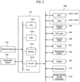
- the controller 121 as a control part is configu red as a computer including a CPU (Central Processing Unit) 121a, a RAM (Random Access Me mory) 121b, a memory 121c and an I/O port 121d.
- the RAM 121b, the memory 121c and the I/O port 121d are configured to be capable of exchanging data with the CPU 121a via an internal bus 121e.
- An input/output device 122 including, for example, a touch panel or the like is connected t o the controller 121.
- an external memory 123 may be connected to the controller 121
- the memory 121c includes, for example, a flash memory, an HDD (Hard Disk Drive), an SSD (Solid State Drive), or the like.
- a control program that controls the operation of the substrate processing apparatus, a process re cipe in which procedures and conditions of substrate processing described below are written, an d the like.
- the process recipe is a combination that causes, by the controller 121, the substrate p rocessing apparatus to execute the respective procedures in a below-described substrate process ing process to obtain a predetermined result.
- the process recipe functions as a program.
- the process recipe, the control program and the like are collectively and simply referred t o as a program.
- the process recipe is simply referred to as a recipe.
- program may mean a case of including the recipe, a case of including the c ontrol program, or a case of including both the recipe and the control program.
- the RAM 121b i configured as a memory area (work area) in which programs, data and the like read by the CP U 121a are temporarily held.
- the I/O port 121d is connected to the MFCs 241a to 241f, the valves 243a to 243f, the pre ssure sensor 245, the APC valve 244, the vacuum pump 246, the temperature sensor 263, the he ater 207, the rotator 267, the boat elevator 115, the shutter opening/closing mechanism 115s, an d the like.
- the CPU 121a is configured to be capable of reading and executing the control program f rom the memory 121c and reading the recipe from the memory 121c in response to an input of a n operation command from the input/output device 122 or the like.
- the CPU 121a is configured to be capable of, according to the contents of the recipe thus read, controlling the flow rate regul ating operations for various substances (various gases) by the MFCs 241a to 241f, the opening/cl osing operations of the valves 243a to 243f, the opening/closing operation of the APC valve 244, the pressure regulating operation by the APC valve 244 based on the pressure sensor 245, the st art and stop of the vacuum pump 246, the temperature regulating operation of the heater 207 ba sed on the temperature sensor 263, the rotation and the rotation speed adjusting operation of th e boat 217 by the rotator 267, the raising and lowering operation of the boat 217 by the boat elev ator 115, the opening/clos
- the controller 121 may be configured by installing, in the computer, the above-described program recorded and stored in an external memory 123.
- the external memory 123 includes, fo r example, a magnetic disk such as a HDD or the like, an optical disk such as a CD or the like, a magneto-optical disk such as an MO or the like, a semiconductor memory such as a USB memor y, a SSD, or the like, and so forth.
- the memory 121c and the external memory 123 are configure d as a computer readable recording medium.
- the memory 121c and the external me mory 123 are collectively and simply referred to as a recording medium.
- the ter m "recording medium” may include the memory 121c, the external memory 123, or both.
- the pr ogram may be provided to the computer by using a communication means such as the Internet o r a dedicated line without using the external memory 123.
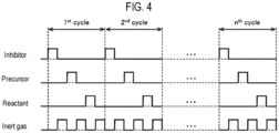
- FIGS. 4 and 5A to 5D An example of a method of processing a substrate, i.e., a processing sequence for formin g a film on a surface of a wafer 200 as a substrate, as a process of manufacturing a semiconducto r device, by using the above-described substrate processing apparatus will be described mainly with reference to FIGS. 4 and 5A to 5D .
- operations of respective co mponents constituting the substrate processing apparatus are controlled by the controller 121.
- a processing sequence includes: performing a cycle a predetermined number of times (n times, where n is an integer equ al to or greater than 1), the cycle including:
- step (reactant supply step) of supplying a reactant to the wafer 200 to modify the first layer into a second layer The processing sequence shown in FIG. 4 will be described as a typical exa mple in which the inhibitor supply step, the precursor supply step, and the reactant supply step are performed in the named order in the above-mentioned cycle.
- inhibitor ⁇ precursor ⁇ reactant ⁇ n may also be denoted as fol lows for the sake of convenience. The same notation is also used in the following description of modifications and other embodiments.
- wafer used herein may refer to "a wafer itself' or "a stacked body of a wafer a nd a predetermined layer or film formed on the surface of the wafer.”
- a surface of a wafer used herein may refer to "a surface of a wafer itself' or "a surface of a predetermined laye r or the like formed on a wafer.”
- the expression “a predetermined layer is formed on a wafer” us ed herein may mean that "a predetermined layer is directly formed on a surface of a wafer itself' or that "a predetermined layer is formed on a layer or the like formed on a wafer”.
- su bstrate used herein may be synonymous with the term "wafer.”
- inhibitor As used herein, terms such as “inhibitor,” “precursor,” “reactant,” and “substance” included e at least one selected from the group of gaseous substances and liquid substances.
- the liquid s ubstances include mist substances. That is, each of the inhibitor, the precursor and the reactant may include gaseous substances, liquid substances such as mist substances or the like, or both of them.
- each of the first layer and the second layer m ay include a continuous layer, a discontinuous layer, or both of them.
- the shutter 21 9s is moved by the shutter opening/closing mechanism 115s to open the lower end opening of th e manifold 209 (shutter opening).
- the boat 217 supporting the pl urality of wafers 200 is lifted by the boat elevator 115 and loaded into the process chamber 201 ( boat loading).
- the seal cap 219 seals the lower end of the manifold 209 via the O-ri ng 220b.
- the wafer 200 is prepared (provided) in the process chamber 201.
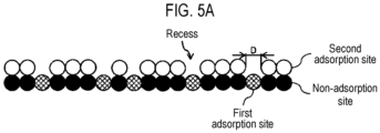
- the surface of the wafer 200 includes recesses of a molecular or ato mic level size.
- First adsorption sites are located at a bottom side of the recesses, and second ads orption sites are located at an upper side of the recesses.
- These adsorption sites include, for exa mple, NH terminations.
- Atoms constituting the second adsorption sites are separated in at least a portion of the s econd adsorption sites, and a distance between the atoms in separation (hereinafter, this distanc e is also referred to as a separation distance D) is shorter than a molecular width (molecular size or molecular diameter) of the precursor supplied to the wafer 200 in the precursor supply step d escribed later. That is, the separation distance D is set such that a molecule of the precursor is n ot able to pass through.
- the atoms constituting the second adsorption sites constitute steric hin drance that inhibits the adsorption (reaching) of the precursor to the first adsorption sites in the precursor supply step described below.
- the above-mentioned separation distance D is longer than a width (molecular si ze or molecular diameter) of a molecule of the intermediate produced from the precursor in the precursor supply step described later, and is longer than a width (molecular size or molecular di ameter) of a molecule of the inhibitor supplied to the wafer 200 in the inhibitor supply step desc ribed later. That is, the separation distance D is set such that each molecule of the intermediate and the inhibitor is not able to pass through.
- the atoms constituting the second adsorption sites do not constitute steric hindrance that inhibits the adsorption (reaching) of the inhibitor to the f irst adsorption sites in the inhibitor supply step described later, and do not constitute steric hin drance that inhibits adsorption (reaching) of the intermediate produced from the precursor to th e first adsorption sites.
- both the first adsorption sites and the second adsorption sites functiono n as adsorption sites capable of adsorbing the inhibitor in the inhibitor supply step described bel ow.
- the first adsorption sites function as adsorption sites that are capable of adsorbi ng the intermediate produced from the precursor but are incapable of adsorbing the precursor i n the precursor supply step described below
- the second adsorption sites function as adsorp tion sites that are capable of adsorbing the precursor and the intermediate in the precursor supp ly step described below.
- the surface of the wafer 200 may be provided with a three-dimensio nal structure such as a hole or a trench.
- a three-dimensio nal structure such as a hole or a trench.
- an entire surface of the three-dimen sional structure is in the above-mentioned surface state. That is, each of upper, side, and botto m surfaces of the hole or the trench in FIG. 7 includes recesses of a molecular or atomic level siz e, as shown in FIG. 5A .
- the above-mentioned first adsorption sites are located at the bottom sid e of each of the recesses, and the above-mentioned second adsorption sites are located at the up per side of each of the recesses.
- an inside of the process chamber 201 i.e., a space w here the wafers 200 are placed, is vacuum-exhausted (decompression-exhausted) by the vacuu m pump 246 so that the pressure inside the process chamber 201 reaches a desired pressure (sta te of vacuum).
- a desired pressure sta te of vacuum
- an internal pressure of the process chamber 201 is measured b y the pressure sensor 245, and the APC valve 244 is feedback-controlled based on pressure infor mation detected.
- the wafers 200 in the process chamber 201 are heated by the he ater 207 to reach a desired processing temperature.
- a state of supplying an ele ctric power to the heater 207 is feedback-controlled based on temperature information detected by the temperature sensor 263 such that a temperature distribution inside the process chamber 201 becomes a desired temperature distribution.
- the rotation of the wafers 200 by th e rotator 267 is started.
- the exhaust of the inside of the process chamber 201 and the heating an d rotation of the wafers 200 may be continuously performed at least until the processing on the wafers 200 is completed.
- the inhibitor is supplied to the wafer 200 that includes the surface including the first adsorption sites and the second adsorption sites.
- valve 243a is opened to allow the inhibitor to flow into the gas supply pi pe 232a.
- a flow rate of the inhibitor is regulated by the MFC 241a.
- the inhibitor is supplied int o the process chamber 201 through the nozzle 249a, and is exhausted from the exhaust port 231 a.
- the inhibitor is supplied to the wafer 200 from a lateral side of the wafer 200 (in hibitor supply).
- the valves 243d to 243f may be opened to supply an inert gas into t he process chamber 201 through the respective nozzles 249a to 249c.
- the inhibitor By supplying the inhibitor under a processing condition shown below to the wafer 200 in cluding the surface described above, it becomes possible to cause the inhibitor to be adsorbed to entire adsorption sites on the surface of the wafer 200, i.e., the first adsorption sites located at t he bottom side of the recesses, and the second adsorption sites located at the upper side of the re Waits. As a result, as shown in FIG. 5B , the entire adsorption sites on the surface of the wafer 2 00 are covered with the inhibitor.
- a processing temperature in the present disclosure means a temperature of the wafer 200 or a temperature inside the process chamber 201
- a processing pressure means a pressu re inside the process chamber 201
- a processing time means a time during which the processing is continued.
- 0 slm when 0 slm is included in the supply flow rate, 0 slm mean s a case where the substance (gas) is not supplied. The same applies to the following description
- the halogen includes at least one selected from the group of fluorine (F), chlorine (Cl), bromine (Br), and iod ine (I).
- the inhibitor may include a fluorine (F 2 ) gas, a chlorine (Cl 2 ) gas, a bromin e (Br 2 ) gas, an iodine (I 2 ) gas, a nitrogen fluoride (NF 3 ) gas, a chlorine fluoride (ClF 3 ) gas, a hydr ogen fluoride (HF) gas, a hydrogen chloride (HCl) gas, a hydrogen bromide (HBr) gas, a hydroge n iodide (HI) gas, and the like.
- a simple halogen an inter-halogen compound, a nitrogen halide, a hydrogen halide, and the like may be used.
- a substance containing amine may be used as the inhibitor.
- the s ubstance containing amine includes carbon (C), nitrogen (N), and hydrogen (H).
- the substance containing amine is also referred to as an amine-based substance (amine-based gas).
- chain amine-based substances such as a triethylami ne ((C 2 H 5 ) 3 N) gas, a diethylamine ((C 2 H 5 ) 2 NH) gas, a monoethylamine ((C 2 H 5 )NH 2 ) gas, a trime thylamine ((CH 3 ) 3 N) gas, a dimethylamine ((CH 3 ) 2 NH) gas, a monomethylamine ((CH 3 )NH 2 ) ga s, and the like may be used.
- chain amine-based substances such as a triethylami ne ((C 2 H 5 ) 3 N) gas, a diethylamine ((C 2 H 5 ) 2 NH) gas, a monoethylamine ((C 2 H 5 )NH 2 ) gas, a trime thylamine ((CH 3 ) 3 N) gas, a dimethylamine ((CH 3 ) 2 NH) gas, a
- One or more of these substances may be used as the inhibitor.
- the molecular size of the inhibitor is preferably smaller than the molecular size of the pr ecursor used in the precursor supply step described below, and is also preferably smaller than th e molecular size of the intermediate produced from the precursor in the precursor supply step.
- a nitrogen (N 2 ) gas, or a rare gas such as an argon (Ar) gas, a helium (He ) gas, a neon (Ne) gas or a xenon (Xe) gas and the like may be used.
- argon (Ar) gas a argon (Ar) gas
- He a helium
- Ne neon
- Xe xenon
- the valve 243a is closed to stop supplying the inhibitor into the process chamber 201. Then, the inside of the process chamber 201 is vacuum-exhausted to remove gaseous substances remai ning inside the process chamber 201 from the inside of the process chamber 201. At this time, t he valves 243d to 243f are opened to supply the inert gas into the process chamber 201 through the nozzles 249a to 249c.
- the inert gas supplied from the nozzles 249a to 249c acts as a purge g as, thereby purging the inside of the process chamber 201 (purging).
- a processing temperature when purging is performed in this step is preferably the same as a processing temperature when the inhibitor is supplied.
- the precursor is supplied to the wafer 200, i. e., the wafer 200 after the inhibitor is adsorbed to the first adsorption sites and the second adsor ption sites.
- valve 243b is opened to allow the precursor to flow into the gas supply pi pe 232b.
- a flow rate of the precursor is regulated by the MFC 241b.
- the precursor is supplied in to the process chamber 201 through the nozzle 249b and is exhausted through the exhaust port 231a.
- the precursor is supplied to the wafer 200 from the lateral side of the wafer 2 00 (precursor supply).
- the valves 243d to 243f may be opened to supply the inert g as into the process chamber 201 through the respective nozzles 249a to 249c.
- the atoms constituting the second adsorption sites constitute the steric hindranc e that inhibits the precursor from reaching the first adsorption sites, as described above. Theref ore, in the precursor supply step, it is possible to suppress the reaction between the inhibitor ads orbed to the first adsorption sites and the precursor.
- a probability of a reaction between the inhibitor adsorbed to the firs t adsorption sites and the intermediate may be made lower than a probability of a reaction betw een the inhibitor adsorbed to the second adsorption sites and the intermediate. Accordingly, in the precursor supply step, it is possible to suppress both a reaction between the inhibitor adsorb ed to the first adsorption sites and the precursor, and the reaction between the inhibitor adsorbe d to the first adsorption sites and the intermediate.
- the precursor supply step it is possible to maintain at least a part of the in hibitor adsorbed to the first adsorption sites by suppressing desorption of the inhibitor from the first adsorption sites, and it is possible to selectively desorb and remove the inhibitor adsorbed t o the second adsorption sites, among the inhibitor adsorbed to the first adsorption sites and the second adsorption sites.
- the precursor supply step by maintaining at least a part of the inhibi tor adsorbed to the first adsorption sites, it is possible to suppress adsorption of the intermediat e to the first adsorption sites, making it possible to keep an adsorption amount (adsorption rate) of the intermediate adsorbed to the second adsorption sites larger (higher) than an adsorption a mount (adsorption rate) of the intermediate adsorbed to the first adsorption sites.
- adsorption amount adsorption rate
- the precursor supply step as shown in FIG. 5C , it becomes possible to selectively cause the pre cursor and the intermediate to be adsorbed to the second adsorption sites while maintaining a st ate in which the first adsorption sites are buried (covered) with the inhibitor.
- the processing condition when supplying the precursor in the precursor supply step are exemplified as follows.
- a substance containing a halogen and a main element con stituting a film may be used.
- the halogen includes at least one selected from the group of fluori ne (F), chlorine (Cl), bromine (Br), and iodine (I).
- the main element constituting a film include s a semiconductor element such as silicon (Si) or the like.
- a gas containing Si and a halogen, i.e., a halosilane-based gas may be used.
- the precursor may include a fluorosilane-based gas such as a diflu orosilane (SiH 2 F 2 ) gas or the like, a chlorosilane-based gas such as a monochlorosilane (SiH 3 Cl) gas, a dichlorosilane (SiH 2 Cl 2 ) gas, a trichlorosilane (SiHCl 3 ) gas, a hexachlorodisilane (Si 2 Cl 6 ) g as, an octachlorotrisilane (Si 3 Cl 8 ) gas or the like, a bromosilane-based gas such as a dibromosila ne (SiH 2 Br 2 ) gas or the like, and an iodosilane-based gas such as diiodosi
- a gas containing Si and an amino group i.e., an a minosilane-based gas
- the precursor may include an aminosilane-base d gas such as a tetrakis(dimethylamino)silane (Si[N(CH 3 ) 2 ] 4 ) gas, a tris(dimethylamino)silane (S i[N(CH 3 ) 2 ] 3 H) gas, a bis(diethylamino)silane (Si[N(C 2 H 5 ) 2 ] 2 H 2 ) gas, a bis(tert-butylamino)silane (SiH 2 [NH(C 4 H 9 )] 2 ) gas, a (diisopropylamino)silane (SiH 3 [N(C 3 H 7 ) 2 ]) gas or the like.
- an aminosilane-base d gas such as a tetrakis(dimethyla
- One or more of these gases may be used as the precursor.
- a substance with a molecular structure such as SiHF, SiF 2 , SiHCl, SiCl 2 , SiHBr, SiBr 2 , S iHI, SiI 2 or the like is produced as the intermediate.
- a substance containing halogen as the inhibitor.
- the valve 243b is closed to st op supplying the precursor into the process chamber 201. Then, gaseous substances or the like r emaining in the process chamber 201 are removed (purging) from the process chamber 201 usin g the same processing procedure and processing condition as those for purging in the inhibitor s upply step.
- a processing temperature when purging is performed in this step is preferably the s ame as a processing temperature when precursor is supplied.
- the reactant is supplied to the wafer 200, i. e., the wafer 200 on which the first layer is formed by selectively adsorbing the precursor and th e intermediate to the second adsorption sites among the adsorption sites on the surface of the w afer 200.
- valve 243c is opened to allow the reactant to flow into the gas supply pip e 232c.
- a flow rate of the reactant is regulated by the MFC 241c.
- the reactant is supplied into th e process chamber 201 through the nozzle 249c and is exhausted through the exhaust port 231a.
- the reactant is supplied to the wafer 200 from the lateral side of the wafer 200 (rea ctant supply).
- the valves 243d to 243f may be opened to supply the inert gas into th e process chamber 201 through the respective nozzles 249a to 249c.
- the inhibitor may not be completely removed f rom the surface of the wafer 200, and a small amount of the inhibitor may remain in the film fin ally formed on the surface of the wafer 200.
- the region from which the inhibitor is removed ma y be filled by adsorption of atoms and molecules that constitute the reactant, or may be filled by migration of atoms and molecules that constitute the precursor.
- the processing condition when supplying the reactant in the reactant supply step are exe mplified as follows.
- a substance containing at least one selected from the group of nitrogen a nd oxygen may be used.
- a nitrogen (N)- and hydrogen (H)-containing substance may be used as the reactant.
- the N- and H-containing substance may include de a hydrogen nitride-based gas such as a diazene (N 2 H 2 ) gas, a hydrazine (N 2 H 4 ) gas, an ammo nia (NH 3 ) gas, a N 3 H 8 gas or the like, an ethylamine-based gas such as a monoethylamine (C 2 H 5 NH 2 ) gas, a diethylamine ((C 2 H 5 ) 2 NH) gas, a triethylamine ((C 2 H 5 ) 3 N) gas or the like, a methyla mine-based gas such as a monomethylamine (CH 3 NH 2 ) gas, a dimethylamine ((CH 3 ) 2 NH) gas, a trimethylamine ((CH 3 ) 3 N) gas or
- an oxygen (O)-containing substance O-containing gas
- O-containing substance may include an oxygen (O 2 ) gas, an o zone (O 3 ) gas, a water vapor (H 2 O gas), a hydrogen peroxide (H 2 O 2 ) gas, a hydrogen (H 2 ) gas + o xygen (O 2 ) gas, a deuterium (D 2 ) gas + oxygen (O 2 ) gas, oxygen radicals (O 2 * or O*), atomic oxyg en (O), and the like.
- the description of two gases together, such as "H 2 gas + O 2 gas" in the pres ent disclosure means a mixed gas of H 2 gas and O 2 gas.
- the two gases When supplying the mixed gas, the two gases may be mixed (premixed) in a supply pipe and then supplied into the process chamber 201 , or the two gases may be separately supplied into the process chamber from different supply pip es and then mixed (post-mixed) within the process chamber 201.
- One or more of these gases may be used as the reactant.
- the N- and H-containing substance when using, for example, the N- and H-containing substance as the reactant, it is preferable to use, for example, a substance containing halogen as the inhibitor, and it is pref erable to use, for example, a halosilane-based gas as the precursor.
- the O-containing substance when using, for e xample, it is preferable to use, for example, a substa nce containing an amine as the inhibitor, and it is preferable to use, for example, an aminosilane -based gas as the precursor.
- the valve 243c is closed to stop supplying the reactant into the process chamber 201. Then, gas eous substances or the like remaining in the process chamber 201 are removed (purging) from t he process chamber 201 using the same processing procedure and processing condition as those for purging in the inhibitor supply step.
- a processing temperature when purging is performed i n this step is preferably the same as a processing temperature when the reactant is supplied.
- n times (where n is an integer of 1 or 2 or more), a cycle that performs th e inhibitor supply step, the precursor supply step and the reactant supply step non-simultaneous ly, i.e., without synchronization, in the named order, it is possible to form a film with a desired c omposition on the surface of the wafer 200.
- a sil icon nitride film SiN film
- a silicon oxide film is formed on the surface of the wafer 200.
- the above-described cycle is performed multiple times. That is, the thickness o f the second layer formed per cycle is set to be thinner than a desired film thickness, and the abo ve-described cycle is performed multiple times until the thickness of the film formed by stacking the second layers reaches the desired film thickness.
- the seal cap 219 is lowered by the boat elevator 115 to open the lower end of t he manifold 209. Then, the processed wafers 200, while being supported by the boat 217, are un loaded from the lower end of the manifold 209 to the outside of the reaction tube 203 (boat unlo ading). After the boat is unloaded, the shutter 219s is moved and the lower end opening of the manifold 209 is sealed by the shutter 219s via the O-ring 220c (shutter closing). The processed wafers 200 are discharged from the boat 217 after being unloaded from the reaction tube 203 (w afer discharging).
- one or more of the following eff ects may be obtained.
- the intermediate is produced by a gas phase reaction, an amount of the inte rmediate supplied is larger in an upper side of a trench, a hole or the like where the space is relat ively wide than in a middle side or a bottom side. Further, the intermediate is adsorbed without being saturated as in a CVD reaction. That is, a relatively large amount of the intermediate tend s to be adsorbed to the upper side of a trench, a hole or the like, and this becomes a factor that d eteriorates the step coverage. This tendency is exacerbated as the amount of the intermediate a dsorbed to the entire adsorption sites of a trench, a hole or the like increases.
- accor ding to the present disclosure it is possible to reduce the adsorption amount (adsorption rate) o f the intermediate adsorbed to the entire adsorption sites including the upper side of a trench, a hole or the like. This makes it possible to suppress the tendency that a relatively large amount o f the intermediate is absorbed to the upper side of a trench, a hole or the like. As a result, it beco mes possible to significantly improve the step coverage.
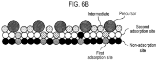
- FIG. 6A is a schematic cross-sectional view showing a surface state of a wafer including, on a surface, first adsorption sites and second adsorption sites.
- the surface state of the wafer sh own in this figure is similar to the surface state of the above-described wafer shown in FIG. 5A .
- the precursor and the intermediate may be adsorbed to the sec ond adsorption sites, and the intermediate may also be adsorbed to the first adsorption sites, as shown in FIG. 6B .
- a first layer formed on the surface of the wafer may con tain a large amount of intermediate components. If the reactant supply step is performed in this state, as shown in FIG. 6C , a second layer formed on the surface of the wafer may contain a large amount of intermediate components, and a step coverage of the second layer may be lower than that of the film formed on the surface of the wafer by the method shown in the embodiments of t he present disclosure. This may make it difficult to form this film into a conformal film.
- the first adsorption sites are located at the bottom side of the recess of the surface of the wafer, and the second adsorption sites are located at the upper side thereof. Therefore, in th e precursor supply step, a reaction probability among the inhibitor adsorbed to the second adsor ption sites, the precursor and the intermediate is possible to be made higher than a reaction pro bability among the inhibitor adsorbed to the first adsorption sites, the precursor and the interm ediate. Thus, in the precursor supply step, it becomes possible to effectively perform selectively desorption and removal of the inhibitor adsorbed to the second adsorption sites and selective ad sorption of the precursor and the intermediate to the second adsorption sites.
- the atoms constituting the second adsorption sites constitute the steric hindrance that inhibi ts adsorption of the precursor to the first adsorption sites.
- the intermediate are able to be adsorbed to the first adsorption sites and the second adsor ption sites in the precursor supply step. Furthermore, in the inhibitor supply step, the inhibitor are able to be adsorbed to the first adsorption sites and the second adsorption sites. As a result, it becomes possible to allow the above-mentioned reaction to occur effectively.
- the inhibitor remaining at the first adsorption sites in the p recursor supply step may be removed by the action of the reactant. As a result, it is possible to s uppress the inhibitor from remaining in the film formed on the surface of the wafer.
- the inhibitor contains halogen and the precursor contains halogen and a main el ement constituting a film, it is possible to allow the above-mentioned reaction to occur effectivel y. Moreover, since the reactant contains at least one selected from the group of nitrogen and ox ygen, it is possible to allow the above-mentioned reaction to occur effectively.
- a predetermined p ost-treatment may be performed on the film formed on the surface of the substrate.
- post-treatment examples include a heat treatment in an atmosphere containing a predetermined post-treatment substance (post-treatment gas), a plasma treatment using a post-treatment substance, and the like.
- post-treatment substance the various reactants menti oned above, for example, reactive gases such as an NH 3 gas, an O 2 gas, a H 2 gas, a D 2 gas and the like, inert gases such as a He gas, an Ar gas, an N 2 gas and the like, and mixtures of these gases may be used.
- reactive gases such as an NH 3 gas, an O 2 gas, a H 2 gas, a D 2 gas and the like
- inert gases such as a He gas, an Ar gas, an N 2 gas and the like
- the post-treatment substance one or more of these gases may be used.
- the po st-treatment may be performed in a same process chamber (in-situ) as the process chamber in w hich the film-forming step is performed, or may be performed in a process chamber (ex-situ) dif ferent from the process chamber in which the film-forming step is performed.
- the RF power refers to a power which is applied to generate plasma when p erforming the plasma treatment using the post-treatment substance.
- a n act of performing an inhibitor supply step and an act of performing a set including a precurso r supply step and a reactant supply step a predetermined number of times (m times where m is a n integer of 1 or 2 or more) may be performed. Also in these embodiments, the same effects as i n the above-described embodiments may be obtained.
- multi-component films such as a silicon oxynitride film (SiON film), a silicon oxycarbonate film (SiOC film), a silicon oxycarb onitride film (SiOCN film), a silicon carbonitride film (SiCN film), a silicon boronitride film (SiB N film), a silicon borocarbonitride film (SiBCN film), a silicon borooxynitride film (SiBON film), a silicon borooxycarbonitride film (SiBOCN film), and the like may be formed on the surface of t he substrate using multiple types of the reactant.
- SiON film silicon oxynitride film
- SiOC film silicon oxycarbonate film
- SiOCN film silicon oxycarb onitride film
- SiCN film silicon carbonitride film
- SiB N film silicon boronitride film
- SiBCN film silicon borocarbonitride film
- SiBON film silicon borooxynitride film
- a carbon (C)-containing gas such as a propylene (C 3 H 6 ) gas or the like
- a b oron (B)-containing gas such as a boron trichloride (BCl 3 ) gas or the like
- films containing metal ele ments such as a hafnium oxide film (HfO film), a zirconium oxide film (ZrO film), an aluminum oxide film (AlO film), a titanium oxide film (TiO film), a tungsten oxide film (WO film), a hafniu m nitride film (HfN film), a zirconium nitride film (ZrN film), an aluminum nitride film (AlN fil m), a titanium nitride film (TiN film), a tungsten nitride film (WN film), a hafnium oxynitride fil m (HfON film), a zirconium oxynitride film (ZrON film), an aluminum oxynitride film (AlON fil m), a titanium oxynitride film (TiON film), a tungsten oxynitride film (WON), an aluminum oxynitride film (
- the recipe used for each process may be prepared separately according to processing con tents and may be recorded and stored in the memory 121c via an electric communication line or the external memory 123.
- the CPU 121a may properly select an app ropriate recipe from a plurality of recipes recorded and stored in the memory 121c according to t he processing contents. This makes it possible to form films of various film types, composition r atios, film qualities and film thicknesses with high reproducibility in one substrate processing ap paratus.
- the burden on an operator may be reduced, and each process may be quick ly started while avoiding operation errors.
- the above-described recipes are not limited to newly prepared ones, but may be prepare d by, for example, changing existing recipes already installed in the substrate processing apparat us.
- the recipes after the change may be installed in the subst rate processing apparatus via an electric communication line or a recording medium in which th e recipes are recorded.
- the input/output device 122 installed in the existing substrat e processing apparatus may be operated to directly change the existing recipes already installed i n the substrate processing apparatus.
- a film is fo rmed by using a batch type substrate processing apparatus configured to process a plurality of s ubstrates at a time.
- the present disclosure is not limited to the above-described embodiments, but may be suitably applied to, for example, a case where a film is formed using a single-wafer ty pe substrate processing apparatus configured to process one or several substrates at a time.
- Fur thermore in the above-described embodiments, there is described the example in which a film i s formed using a substrate processing apparatus including a hot-wall-type process furnace.
- the present disclosure is not limited to the above-described embodiments, but may also be suitably applied to a case where a film is formed using a substrate processing apparatus including a cold -wall-type process furnace.
- each process may be perfor med under the processing procedures and processing conditions as those of the above-described embodiments and modifications.
- the same effects as those of the above-described embodiment s and modifications may be obtained.
- the above-described embodiment and modifications may be used in combination as app ropriate.
- the processing procedures and processing conditions at this time may be, for example , the same as the processing procedures and processing conditions of the above-described embo diments and modifications.
Landscapes
- Chemical & Material Sciences (AREA)
- General Chemical & Material Sciences (AREA)
- Chemical Kinetics & Catalysis (AREA)
- Engineering & Computer Science (AREA)
- Materials Engineering (AREA)
- Mechanical Engineering (AREA)
- Metallurgy (AREA)
- Organic Chemistry (AREA)
- Inorganic Chemistry (AREA)
- Chemical Vapour Deposition (AREA)
- Container, Conveyance, Adherence, Positioning, Of Wafer (AREA)
- Formation Of Insulating Films (AREA)
Applications Claiming Priority (1)
| Application Number | Priority Date | Filing Date | Title |
|---|---|---|---|
| JP2023026842A JP2024120206A (ja) | 2023-02-24 | 2023-02-24 | 基板処理方法、半導体装置の製造方法、基板処理装置、およびプログラム |
Publications (1)
| Publication Number | Publication Date |
|---|---|
| EP4435142A1 true EP4435142A1 (de) | 2024-09-25 |
Family
ID=89853492
Family Applications (1)
| Application Number | Title | Priority Date | Filing Date |
|---|---|---|---|
| EP24155984.8A Pending EP4435142A1 (de) | 2023-02-24 | 2024-02-06 | Verfahren zur substratverarbeitung, verfahren zur herstellung eines halbleiterbauelements, substratverarbeitungsvorrichtung und programm |
Country Status (6)
| Country | Link |
|---|---|
| US (1) | US20240287676A1 (de) |
| EP (1) | EP4435142A1 (de) |
| JP (1) | JP2024120206A (de) |
| KR (1) | KR20240131889A (de) |
| CN (1) | CN118553599A (de) |
| TW (1) | TW202510090A (de) |
Citations (2)
| Publication number | Priority date | Publication date | Assignee | Title |
|---|---|---|---|---|
| US20160148800A1 (en) * | 2014-11-24 | 2016-05-26 | Lam Research Corporation | Selective inhibition in atomic layer deposition of silicon-containing films |
| US20220230870A1 (en) * | 2021-01-18 | 2022-07-21 | Kokusai Electric Corporation | Method of manufacturing semiconductor device, substrate processing method, substrate processing apparatus, and recording medium |
Family Cites Families (8)
| Publication number | Priority date | Publication date | Assignee | Title |
|---|---|---|---|---|
| JP6436887B2 (ja) | 2015-09-30 | 2018-12-12 | 株式会社Kokusai Electric | 半導体装置の製造方法、基板処理装置、ガス供給システムおよびプログラム |
| JP6778144B2 (ja) * | 2017-04-25 | 2020-10-28 | 株式会社Kokusai Electric | 半導体装置の製造方法、基板処理装置およびプログラム |
| JP6789257B2 (ja) * | 2018-02-28 | 2020-11-25 | 株式会社Kokusai Electric | 半導体装置の製造方法、基板処理装置、およびプログラム |
| JP7085929B2 (ja) * | 2018-07-13 | 2022-06-17 | 東京エレクトロン株式会社 | 成膜方法 |
| JP7023905B2 (ja) * | 2019-08-30 | 2022-02-22 | 株式会社Kokusai Electric | 半導体装置の製造方法、基板処理方法、基板処理装置、およびプログラム |
| JP7304905B2 (ja) * | 2021-01-29 | 2023-07-07 | 株式会社Kokusai Electric | 基板処理方法、半導体装置の製造方法、基板処理装置、およびプログラム |
| JP7194216B2 (ja) * | 2021-03-17 | 2022-12-21 | 株式会社Kokusai Electric | 半導体装置の製造方法、基板処理方法、プログラム及び基板処理装置 |
| JP7273086B2 (ja) * | 2021-03-24 | 2023-05-12 | 株式会社Kokusai Electric | 半導体装置の製造方法、プログラム及び基板処理装置 |
-
2023
- 2023-02-24 JP JP2023026842A patent/JP2024120206A/ja active Pending
- 2023-12-21 CN CN202311772735.1A patent/CN118553599A/zh active Pending
-
2024
- 2024-01-16 TW TW113101621A patent/TW202510090A/zh unknown
- 2024-02-05 KR KR1020240017322A patent/KR20240131889A/ko active Pending
- 2024-02-06 EP EP24155984.8A patent/EP4435142A1/de active Pending
- 2024-02-15 US US18/442,761 patent/US20240287676A1/en active Pending
Patent Citations (2)
| Publication number | Priority date | Publication date | Assignee | Title |
|---|---|---|---|---|
| US20160148800A1 (en) * | 2014-11-24 | 2016-05-26 | Lam Research Corporation | Selective inhibition in atomic layer deposition of silicon-containing films |
| US20220230870A1 (en) * | 2021-01-18 | 2022-07-21 | Kokusai Electric Corporation | Method of manufacturing semiconductor device, substrate processing method, substrate processing apparatus, and recording medium |
Non-Patent Citations (2)
| Title |
|---|
| KHAN RIZWAN ET AL: "Area-Selective Atomic Layer Deposition Using Si Precursors as Inhibitors", CHEMISTRY OF MATERIALS, vol. 30, no. 21, 11 October 2018 (2018-10-11), US, pages 7603 - 7610, XP093004183, ISSN: 0897-4756, DOI: 10.1021/acs.chemmater.8b02774 * |
| YARBROUGH JOSIAH ET AL: "Tuning Molecular Inhibitors and Aluminum Precursors for the Area-Selective Atomic Layer Deposition of Al 2 O 3", CHEMISTRY OF MATERIALS, vol. 34, no. 10, 10 May 2022 (2022-05-10), US, pages 4646 - 4659, XP093185841, ISSN: 0897-4756, Retrieved from the Internet <URL:https://pubs.acs.org/doi/pdf/10.1021/acs.chemmater.2c00513> DOI: 10.1021/acs.chemmater.2c00513 * |
Also Published As
| Publication number | Publication date |
|---|---|
| TW202510090A (zh) | 2025-03-01 |
| US20240287676A1 (en) | 2024-08-29 |
| CN118553599A (zh) | 2024-08-27 |
| KR20240131889A (ko) | 2024-09-02 |
| JP2024120206A (ja) | 2024-09-05 |
Similar Documents
| Publication | Publication Date | Title |
|---|---|---|
| KR102513888B1 (ko) | 기판 처리 방법, 반도체 장치의 제조 방법, 기판 처리 장치 및 프로그램 | |
| US20250299948A1 (en) | Method of manufacturing semiconductor device, substrate processing method, substrate processing apparatus, and recording medium | |
| KR102345313B1 (ko) | 반도체 장치의 제조 방법, 기판 처리 장치 및 프로그램 | |
| KR102895610B1 (ko) | 기판 처리 방법, 반도체 장치의 제조 방법, 기판 처리 장치, 및 프로그램 | |
| CN114561630B (zh) | 半导体器件的制造方法、衬底处理方法、记录介质及衬底处理装置 | |
| KR102540741B1 (ko) | 반도체 장치의 제조 방법, 기판 처리 방법, 프로그램 및 기판 처리 장치 | |
| KR102264071B1 (ko) | 클리닝 방법, 반도체 장치의 제조 방법, 기판 처리 장치 및 프로그램 | |
| KR102224893B1 (ko) | 처리 용기 내의 부재를 클리닝하는 방법, 반도체 장치의 제조 방법, 기판 처리 장치, 및 프로그램 | |
| KR20200073153A (ko) | 반도체 장치의 제조 방법, 표면 처리 방법, 기판 처리 장치, 및 프로그램 | |
| KR20220144311A (ko) | 기판 처리 방법, 반도체 장치의 제조 방법, 기판 처리 장치 및 프로그램 | |
| WO2011093203A1 (ja) | 半導体装置の製造方法、基板処理装置及び半導体装置 | |
| KR20210119301A (ko) | 반도체 장치의 제조 방법, 기판 처리 장치 및 프로그램 | |
| CN117702084A (zh) | 衬底处理方法、半导体器件的制造方法、衬底处理装置及记录介质 | |
| TWI831204B (zh) | 半導體裝置之製造方法、基板處理方法、基板處理裝置及程式 | |
| KR102916947B1 (ko) | 기판 처리 방법, 반도체 장치의 제조 방법, 기판 처리 장치 및 프로그램 | |
| EP4435142A1 (de) | Verfahren zur substratverarbeitung, verfahren zur herstellung eines halbleiterbauelements, substratverarbeitungsvorrichtung und programm | |
| US20240318306A1 (en) | Substrate processing apparatus, method of manufacturing semiconductor device, and recording medium | |
| JP7751073B2 (ja) | 基板処理方法、半導体装置の製造方法、プログラム、および基板処理装置 | |
| CN113363151B (zh) | 半导体器件的制造方法、衬底处理装置及记录介质 | |
| KR20220029484A (ko) | 클리닝 방법, 반도체 장치의 제조 방법, 기판 처리 장치 및 프로그램 | |
| KR102840946B1 (ko) | 기판 처리 방법, 반도체 장치의 제조 방법, 기판 처리 장치 및 프로그램 | |
| JP7135190B2 (ja) | 半導体装置の製造方法、基板処理方法、基板処理装置、およびプログラム | |
| JP7305013B2 (ja) | 基板処理方法、半導体装置の製造方法、基板処理装置、およびプログラム | |
| KR102865581B1 (ko) | 기판 처리 방법, 반도체 장치의 제조 방법, 기판 처리 장치, 및 프로그램 | |
| JP7186909B2 (ja) | 基板処理方法、半導体装置の製造方法、基板処理装置、およびプログラム |
Legal Events
| Date | Code | Title | Description |
|---|---|---|---|
| PUAI | Public reference made under article 153(3) epc to a published international application that has entered the european phase |
Free format text: ORIGINAL CODE: 0009012 |
|
| STAA | Information on the status of an ep patent application or granted ep patent |
Free format text: STATUS: REQUEST FOR EXAMINATION WAS MADE |
|
| 17P | Request for examination filed |
Effective date: 20240305 |
|
| AK | Designated contracting states |
Kind code of ref document: A1 Designated state(s): AL AT BE BG CH CY CZ DE DK EE ES FI FR GB GR HR HU IE IS IT LI LT LU LV MC ME MK MT NL NO PL PT RO RS SE SI SK SM TR |
|
| P01 | Opt-out of the competence of the unified patent court (upc) registered |
Free format text: CASE NUMBER: APP_25396/2025 Effective date: 20250528 |