EP4432565A2 - High-order phase tracking loop with segmented proportional and integral controls - Google Patents
High-order phase tracking loop with segmented proportional and integral controls Download PDFInfo
- Publication number
- EP4432565A2 EP4432565A2 EP24190984.5A EP24190984A EP4432565A2 EP 4432565 A2 EP4432565 A2 EP 4432565A2 EP 24190984 A EP24190984 A EP 24190984A EP 4432565 A2 EP4432565 A2 EP 4432565A2
- Authority
- EP
- European Patent Office
- Prior art keywords
- clock
- phase
- signal
- digital
- pll
- Prior art date
- Legal status (The legal status is an assumption and is not a legal conclusion. Google has not performed a legal analysis and makes no representation as to the accuracy of the status listed.)
- Pending
Links
Images





Classifications
-
- H—ELECTRICITY
- H03—ELECTRONIC CIRCUITRY
- H03L—AUTOMATIC CONTROL, STARTING, SYNCHRONISATION OR STABILISATION OF GENERATORS OF ELECTRONIC OSCILLATIONS OR PULSES
- H03L7/00—Automatic control of frequency or phase; Synchronisation
- H03L7/06—Automatic control of frequency or phase; Synchronisation using a reference signal applied to a frequency- or phase-locked loop
- H03L7/08—Details of the phase-locked loop
- H03L7/081—Details of the phase-locked loop provided with an additional controlled phase shifter
-
- H—ELECTRICITY
- H03—ELECTRONIC CIRCUITRY
- H03L—AUTOMATIC CONTROL, STARTING, SYNCHRONISATION OR STABILISATION OF GENERATORS OF ELECTRONIC OSCILLATIONS OR PULSES
- H03L7/00—Automatic control of frequency or phase; Synchronisation
- H03L7/06—Automatic control of frequency or phase; Synchronisation using a reference signal applied to a frequency- or phase-locked loop
- H03L7/08—Details of the phase-locked loop
- H03L7/081—Details of the phase-locked loop provided with an additional controlled phase shifter
- H03L7/0812—Details of the phase-locked loop provided with an additional controlled phase shifter and where no voltage or current controlled oscillator is used
- H03L7/0814—Details of the phase-locked loop provided with an additional controlled phase shifter and where no voltage or current controlled oscillator is used the phase shifting device being digitally controlled
-
- H—ELECTRICITY
- H03—ELECTRONIC CIRCUITRY
- H03L—AUTOMATIC CONTROL, STARTING, SYNCHRONISATION OR STABILISATION OF GENERATORS OF ELECTRONIC OSCILLATIONS OR PULSES
- H03L7/00—Automatic control of frequency or phase; Synchronisation
- H03L7/06—Automatic control of frequency or phase; Synchronisation using a reference signal applied to a frequency- or phase-locked loop
- H03L7/08—Details of the phase-locked loop
- H03L7/085—Details of the phase-locked loop concerning mainly the frequency- or phase-detection arrangement including the filtering or amplification of its output signal
- H03L7/087—Details of the phase-locked loop concerning mainly the frequency- or phase-detection arrangement including the filtering or amplification of its output signal using at least two phase detectors or a frequency and phase detector in the loop
-
- H—ELECTRICITY
- H03—ELECTRONIC CIRCUITRY
- H03L—AUTOMATIC CONTROL, STARTING, SYNCHRONISATION OR STABILISATION OF GENERATORS OF ELECTRONIC OSCILLATIONS OR PULSES
- H03L7/00—Automatic control of frequency or phase; Synchronisation
- H03L7/06—Automatic control of frequency or phase; Synchronisation using a reference signal applied to a frequency- or phase-locked loop
- H03L7/08—Details of the phase-locked loop
- H03L7/085—Details of the phase-locked loop concerning mainly the frequency- or phase-detection arrangement including the filtering or amplification of its output signal
- H03L7/093—Details of the phase-locked loop concerning mainly the frequency- or phase-detection arrangement including the filtering or amplification of its output signal using special filtering or amplification characteristics in the loop
-
- H—ELECTRICITY
- H03—ELECTRONIC CIRCUITRY
- H03L—AUTOMATIC CONTROL, STARTING, SYNCHRONISATION OR STABILISATION OF GENERATORS OF ELECTRONIC OSCILLATIONS OR PULSES
- H03L7/00—Automatic control of frequency or phase; Synchronisation
- H03L7/06—Automatic control of frequency or phase; Synchronisation using a reference signal applied to a frequency- or phase-locked loop
- H03L7/08—Details of the phase-locked loop
- H03L7/099—Details of the phase-locked loop concerning mainly the controlled oscillator of the loop
- H03L7/0991—Details of the phase-locked loop concerning mainly the controlled oscillator of the loop the oscillator being a digital oscillator, e.g. composed of a fixed oscillator followed by a variable frequency divider
- H03L7/0994—Details of the phase-locked loop concerning mainly the controlled oscillator of the loop the oscillator being a digital oscillator, e.g. composed of a fixed oscillator followed by a variable frequency divider comprising an accumulator
-
- H—ELECTRICITY
- H03—ELECTRONIC CIRCUITRY
- H03L—AUTOMATIC CONTROL, STARTING, SYNCHRONISATION OR STABILISATION OF GENERATORS OF ELECTRONIC OSCILLATIONS OR PULSES
- H03L7/00—Automatic control of frequency or phase; Synchronisation
- H03L7/06—Automatic control of frequency or phase; Synchronisation using a reference signal applied to a frequency- or phase-locked loop
- H03L7/16—Indirect frequency synthesis, i.e. generating a desired one of a number of predetermined frequencies using a frequency- or phase-locked loop
- H03L7/18—Indirect frequency synthesis, i.e. generating a desired one of a number of predetermined frequencies using a frequency- or phase-locked loop using a frequency divider or counter in the loop
-
- H—ELECTRICITY
- H03—ELECTRONIC CIRCUITRY
- H03L—AUTOMATIC CONTROL, STARTING, SYNCHRONISATION OR STABILISATION OF GENERATORS OF ELECTRONIC OSCILLATIONS OR PULSES
- H03L7/00—Automatic control of frequency or phase; Synchronisation
- H03L7/06—Automatic control of frequency or phase; Synchronisation using a reference signal applied to a frequency- or phase-locked loop
- H03L7/16—Indirect frequency synthesis, i.e. generating a desired one of a number of predetermined frequencies using a frequency- or phase-locked loop
- H03L7/22—Indirect frequency synthesis, i.e. generating a desired one of a number of predetermined frequencies using a frequency- or phase-locked loop using more than one loop
-
- H—ELECTRICITY
- H03—ELECTRONIC CIRCUITRY
- H03J—TUNING RESONANT CIRCUITS; SELECTING RESONANT CIRCUITS
- H03J2200/00—Indexing scheme relating to tuning resonant circuits and selecting resonant circuits
- H03J2200/11—Cellular receiver, e.g. GSM, combined with a GPS receiver
Definitions
- a phase locked loop is employed to produce a synchronized clock signal that has a phase matched with that of a reference clock signal, typically the synchronized clock signal has a higher frequency than the frequency of the reference clock signal.
- the reference clock signal can be provided by an onboard reference clock coupled to a PLL device.
- the synchronized clock signal can be matched to the phase of source clock information obtained through synchronous Ethernet (SyncE), or from a precision time protocol (PTP), such as a protocol based on the IEEE 1588 standard.
- SynE synchronous Ethernet
- PTP precision time protocol
- the synchronized clock signal can be used to drive various operations performed by apparatus providing receive/transmit or input/output data transfers, for example in a transceiver or in a serializer-deserializer (SerDes) input/output component in a digital system.
- apparatus providing receive/transmit or input/output data transfers, for example in a transceiver or in a serializer-deserializer (SerDes) input/output component in a digital system.
- the transceiver include an optical transceiver, a wireless transceiver, etc.
- such a synchronized clock signal provided by a PLL device can be used to drive a Digital to Analog Converter (DAC) to send digital data over a link.
- DAC Digital to Analog Converter
- the PLL device is said to be used for clock generation and the synchronized clock signal is said to provide a transmitter clock signal.
- such a synchronized clock signal provided by a PLL device can be used to drive an Analog to Digital Converter (ADC) to sample an input signal received over a link (electrical connection, optical cable, wireless Radio Frequency beam, etc.)
- ADC Analog to Digital Converter
- the synchronized clock signal needs to be phase matched and frequency matched to a transmitter clock signal as received at a local receiver as part of the input signal received.
- the PLL device in such a receiver is said to be used for clock extraction and the synchronized clock signal is said to provide a receiver clock signal.
- Clock generation can also be used to drive clock trees for example.
- an analog phase locked loop (PLL) device includes a voltage-controlled oscillator (VCO) component that generates a VCO output signal which is signal processed to provide the synchronized clock signal based on the reference clock signal.
- VCO voltage-controlled oscillator
- FIG. 1A illustrates a generic PLL device 100.
- a reference clock signal 105 can include a voltage signal from an onboard or external reference clock source (not shown) to which the phase of the synchronized clock signal 180 of the PLL device 100 is intended to lock to.
- the reference clock source can be software and/or hardware, such as an integrated circuit, that includes functionality for generating and/or providing timing information to the PLL device 100.
- a hardware reference clock source can include a crystal oscillator or a global position system (GPS) receiver.
- Software examples of reference clock sources include an implementation of a network protocol over a communications network for synchronizing clocks, such as synchronous Ethernet (SyncE), or an implementation of a precision time protocol (PTP) for example compliant to the IEEE 1588 standard.
- SynE synchronous Ethernet
- PTP precision time protocol
- the analog PLL device 100 operates in a signal processing loop which progressively, over a number of loop cycles, adjusts the VCO output signal to provide the synchronized clock signal.
- the signal processing loop of the PLL device 100 includes an analog phase detector 110 employed to extract a difference between a feedback copy 247 of a VCO output signal 180 and the reference clock signal 105. While an analog phase detector 110 is shown inside the PLL device 100 in Figure 1 , in other implementations an analog phase-frequency detector can be used instead. A phase-frequency detector inside the PLL device 100 can produce two signals that correspond to the phase difference and a frequency difference rather than a single phase difference signal. In other implementations, a digital phase detector can be used instead of the analog phase detector 110 with due changes in the operation of the PLL device 100 and feedback loop.
- a feedback divider includes hardware, such as an integrated circuit, having functionality to divide the frequency of an input signal by an N-multiple.
- the input signal of the feedback divider 145 is output signal 180 and such division by the feedback divider 145 produces a corresponding feedback signal 247 which is a copy of the output signal 180 at a lower frequency.
- the PLL device 100 and particularly the VCO 140, multiplies the reference signal 105 by an N-multiplier to generate the output signal 180.
- feedback divider 145 accounts for the increased frequency of the output signal 180 in order to return feedback signal 247 as an input to the analog phase detector 110 at a similar frequency as that of reference signal 105.
- a cascaded feedback divider 147 is illustrated to further divide the frequency in feedback loop by another M-multiple.
- the PLL device 100 also includes a charge pump 120, a loop filter 130 and various other PLL components (some shown in more detail below).
- a feedback signal path between the output of the VCO 140 and the analog phase detector 110 can include one or more feedback dividers 145, 147.
- the charge pump 120 includes hardware that provides functionality to generate a current signal from a voltage signal, e.g., a current signal that relates to the phase difference (and the frequency difference) detected by the analog phase detector 110.
- the loop filter 130 includes hardware having functionality to check stability within the PLL device 100 as well to operate as a frequency bandwidth limiter to synchronize the output signal 180 with the reference signal 105.
- loop filter 130 includes a low pass filter that operates according to a current signal produced by the charge pump 120 to output a signal. In this sense, the analog PLL device 100 synchronizes to the reference clock signal with a high bandwidth to reduce (VCO) phase noise.
- the voltage-controlled oscillator device 140 includes hardware having functionality to generate an oscillating signal (180) typically at a higher frequency than that of the reference clock signal 105.
- the voltage-controlled oscillator device 140 can include functionality to obtain the signal from the loop filter 130 to generate the output signal 180 with a predefined period and frequency.
- the PLL device 100 can provide a lock signal output by steady-state detector 157 indicative of startup (unsettled, unlocked) and steady-state (settled, locked) operation.
- the steady-state detector 157 can be hardware and/or software that includes functionality to determine whether the output signal 180 is in a steady-state mode. In the steady-state mode, the phase (and frequency) of the output signal 180 may be locked to the reference signal 105. For example, an amount of phase error and/or frequency error may have converged to a (local) minimum where the output signal 180 is approximately phase matched and frequency fixed with respect to the reference signal 105.
- the PLL device 100 when the PLL device 100 is in a transient mode, the PLL device 100 may be adjusting the phase and/or frequency of the output signal 180 to match the reference signal 105. Typically, in transient mode the oscillator of the VCO 140 may have just been turned on and may not have settled yet.
- the PLL device 100 is used for clock generation.
- output signal 180 can be an extracted clock signal obtained using the reference signal 105.
- the VCO 140 is not a perfect oscillator and other elements in the PLL loop of the PLL device 100 are not perfect in their operation either.
- the feedback path is used to provide information from the output 180 of the PLL device 100, typically a copy 247 of the output signal 180, back to the input of the PLL device 100 for comparison with the reference clock signal 105 repeatedly in a loop.
- the output signal 180 In clock generation applications it is desired for the output signal 180 to be ideal in the sense of having a fixed frequency locked to the phase of the reference clock signal 105. In practice however, the output signal 180 has departures from an ideal waveform, departures which are referred throughout herein as jitter. Feedback control is employed to reduce/suppress and preferably reject/canceljitter in the PLL loop. In clock extraction applications it is desired for the output signal 180 to track the remote transmitter clock. Feedback control is employed in order to follow the remote transmitter clock to reduce/suppress and preferably reject/cancel dynamic jitter between the remote transmitter clock (as received) and the output signal 180.
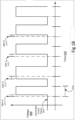
- FIG. 1B schematically illustrates an example of a timing diagram of the output signal 180 obtained during phase locked operation of the PLL device 100.
- a generated output signal 640 output signal 180
- a desired ideal (output) signal 630 along a time axis and another axis for example with respect to voltage.
- the desired ideal signal 630 is not a physical signal in an I/O or transceiver apparatus, and the reference clock signal 105 typically has lower frequency than the ideal signal 630.
- the ideal signal period 630 is constant, for various periods the generated output signal 640 may deviate from the ideal signal period 630.
- the generated output signal 640 includes various amounts of PLL noise i.e., jitter 611, jitter 612, jitter 613, jitter 614 identifying departures of the generated output signal 640 from the ideal signal period 630. While time-interval error jitter is shown by jitter 611, jitter 612, jitter 613, and/or jitter 614, other types of jitter may also exist in the generated output signal 640, such as cycle-to-cycle period jitter, long term jitter, phase jitter, and any other forms of phase noise.
- PLL noise i.e., jitter 611, jitter 612, jitter 613, jitter 614 identifying departures of the generated output signal 640 from the ideal signal period 630. While time-interval error jitter is shown by jitter 611, jitter 612, jitter 613, and/or jitter 614, other types of jitter may also exist in the generated output signal
- FIG. 2A illustrates a block diagram of a transmitter apparatus.
- a clock circuit 295 includes PLL device 100 providing clock generation.
- Clock circuit 295 can be a portion of an I/O or a transceiver apparatus that includes hardware and/or software for transmitting a clock signal within the same or to another computing device.
- Output signal 180 of the PLL device 100 is employed to provide cadence to a digital-to-analog converter (DAC) which includes hardware and/or software to output digital data as an output signal TxSignalOut for transmission over a link.
- DAC digital-to-analog converter
- output signal 180 of clock circuit 295 can be used to drive (not shown) a clock tree (without the use of a DAC).
- the PLL jitter ( Figure 1B ) of clock circuit 295 can be regarded as clock generation jitter.
- a VCO 140 is used in a PLL loop for data signal extraction at a local receiver.
- the data clock of the local receiver at the near end of the link needs to follow the data clock of the remote transmitter at the far end of the link.
- the input signal received from the remote transmitter includes both data sent and a transmitter clock signal of the remote transmitter; the PLL device 100 is employed to extract the transmitter clock signal from the input signal.
- the output signal 180 of the VCO device 140 is employed to provide cadence to an analog-to-digital converter ADC which includes hardware and/or software to convert the received input signal to a digital data output signal providing data extraction from the received input signal. It is desired for the output signal 180 of the PLL device 100 to have a frequency matched to the frequency of the received input signal and phase locked to the phase of the received input signal. In practice however the output signal 180 has departures from the received input signal, departures which are referred herein as clock recovery jitter.
- the data clock of the remote transmitter can be, and typically is, noisy including transmitter jitter for example as described hereinabove. It is emphasized that any transmitter data clock signal, ideal (theoretical) or noisy (practical), can only be seen at the local receiver through the physical link between the remote transmitter and the local receiver, physical link which itself is noisy. A simplification herein is that the local receiver cannot distinguish between remote transmitter jitter and link jitter.
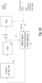
- a common way of implementing clock recovery in a receiver is by directly controlling the VCO 140 through a proportional/integral controller in a manner summarily illustrated in Figure 2B .
- the VCO 140 is controlled directly.
- a digital phase detector 210 (typically Godard type) extracts the transmitter clock from the received input signal and the output of the digital phase detector 210 is used by a proportional/integral controller 222 to adjust the receiver VCO 140 directly.
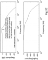
- FIG. 2C illustrates peaking in the clock recovery provided by prior art attempts such as illustrated in Figure 2B .
- Excessive signal processing delay in the loop limits clock recovery bandwidth.
- the achievable bandwidth of such a clock recovery loop needs to be limited to a low value to avoid excessive peaking.
- Limiting clock recovery bandwidth directly affects the overall jitter rejection in the PLL loop since a small bandwidth limits the amount of VCO phase noise suppression which follows a high-pass transfer function.
- One aspect of the solution proposed herein includes emulating a VCO as part of a digital control loop.
- Another aspect of the proposed solution proposed herein includes splitting feedback loop control in two.
- a method for operating a clock circuit is presented which emulates digitally the operation of a VCO with a digital accumulator followed by segmented controls providing proportional and integral loop control functions.
- a combination of a phase rotator and an accumulator is employed to perform frequency tracking (integral path) and a fine digitally controlled delay element is employed to perform the phase tracking (proportional path).
- apparatus including a phased locked loop (PLL) device having a first reference clock signal and a signal processing system coupled to the PLL device.
- the signal processing system obtains an output signal from the PLL device.
- the signal processing system further determines, using a digital phase detector operating on a copy of the output signal and second reference clock signal clock signal to determine an amount of phase difference between the output signal and second reference clock signal.
- the processing system employs the digital phase detector and a digital accumulator to combine multiple phased differences in an integration window (integral path) to filter, using a phase rotator, a portion of the amount of phase difference from the output signal to generate a filtered signal.
- the embodiments employ a digitally controlled fine delay element to provide additional signal filtering (proportional path) in the feedback loop of the PLL device.
- the output of the same digital phase detector is also employed to control the delay element.
- Clock circuit implementations in which the second reference clock signal is a copy of the first reference clock signal can provide clock generation in a transmitter.
- Clock circuit implementations in which the second reference clock signal is a transmitter clock signal received from a remote transmitter provide clock extraction in a receiver.
- ordinal numbers e.g., first, second, third, etc.
- an element i.e., any noun in the application.
- the use of ordinal numbers is not to imply or create any particular ordering of the elements nor to limit any element to being only a single element unless expressly disclosed, such as by the use of the terms "before”, “after”, “single”, and other such terminology. Rather, the use of ordinal numbers is to distinguish between the elements.
- a first element is distinct from a second element, and the first element may encompass more than one element and succeed (or precede) the second element in an ordering of elements.
- Embodiments of the proposed solution provide systems, apparatus, clock circuits and signal processing methods indirectly controlling VCO of a PLL device via a feedback path in a PLL loop.
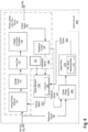
- a clock recovery circuit 395 which includes a phase rotator 115 disposed within the feedback loop of a phase locked loop (PLL) device 100.
- a digital phase detector 160 coupled to the phase rotator 115 is employed to determine a frequency offset and/or phase misalignment between a transmitter clock signal 185, as received at the receiver, and a copy 187 of the output signal 180 of the PLL device 100.
- the clock circuit 395 provides output signal 180, the synchronized output signal, as a receiver clock signal (187) to an ADC.
- a phase rotator 115 is configured to apply a phase shift correction in the feedback loop to reduce the frequency offset and/or phase misalignment between the transmitter clock signal 185 and the receiver clock signal 187.
- the phase rotator 115 provides filtered signal 155 as the feedback signal to the PLL device 100.
- the PLL device 100 includes analog phase detector 110, for example an integrated circuit including functionality to determine a difference in phase between two input signals e.g., reference clock signal 105 and filtered signal 155 fed back from the VCO 140 output.
- analog phase detector 110 for example an integrated circuit including functionality to determine a difference in phase between two input signals e.g., reference clock signal 105 and filtered signal 155 fed back from the VCO 140 output.
- the phase rotator based digital clock recovery provided allows the clock circuit 395 to lock to a locally received data signal generated by a remote transmitter PLL locked to a reference clock different from the reference clock (105) of the receiver PLL device 100.
- the digital phase detector 160 is employed in the clock circuit 395 to provide clock recovery in a receiver.
- the digital phase detector 160 includes hardware and/or software that implements functionality to determine an amount of phase difference between transmitter clock signal 185 and the receiver clock signal 187 which is a feedback copy of output signal 180.
- the clock circuit further includes a digital accumulator 165 coupled to the digital phase detector 160.
- the phase rotator 115 and the digital accumulator 165 using the amount of phase difference between the transmitter clock signal 185 and the receiver clock signal 187 (output signal 180), filter a portion of the amount of phase difference from another copy 246 of the output signal 180 (feedback divider not shown) to generate a filtered signal 155 which is provided to the analog phase detector 110.
- the phase rotator digital PLL locks to the transmitter clock signal 185.
- the transmitter clock signal 185 is embedded with the data signal in the signal received over the link.
- This configuration of clock circuit 395 decouples the high bandwidth requirement of the analog PLL 100 to reject the phase noise of the VCO 140 from the requirement of the clock recovery bandwidth of the phase rotator digital PLL.
- the phase rotator based digital clock recovery bandwidth is selected to balance jitter tracking with respect to the transmitter clock signal 185 as received vs. jitter rejection of the VCO/PLL jitter.
- digital phase detector 160 itself is not a perfect device.
- digital phase detector error can be reduced through averaging, or integration, the result being understood to provide integral control.
- phase rotator 115 includes hardware providing functionality to adjust a frequency offset and/or phase misalignment between transmitter clock signal 185 and a receiver clock signal 187 (a copy of output signal 180).
- phase rotator 115 includes one or more hardware components that include functionality to apply a predetermined amount of phase shift to feedback copy 246 of output signal 180 based on control signal 151.
- a phase rotator includes a pair of variable gain amplifiers that apply predetermined weights to an in-phase (I) component and a quadrature (Q) component of an input signal, a feedback copy of output signal 180.
- a phase rotator is configured to generate a pair of differential phase signals from its input signal that correspond to the I component (i.e., "I phase signal”) and the Q component (i.e., "Q phase signal”) of the input signal.
- the I phase signal and the Q phase signal are expressed using the following equations:
- A is the amplitude of an output signal from the phase rotator 115, such as filtered signal 155;
- k is a gain value in the phase rotator
- v ( t ) is the voltage of the input signal
- t is the time domain
- ⁇ is the phase shift applied to feedback signal 246 (output signal 180) by the phase rotator 115.
- the I phase signal and/or the Q phase signal may be generated within the phase rotator 115 for example by a resistor-capacitor (RC) polyphase network, frequency dividers, and/or a resistor-capacitor pairs.
- the phase rotator 115 can include an interpolator circuit that generates a linear summation of the I phase signal and the Q phase signal.
- the phase rotator 115 produces filtered signal 155 with the applied phase shift as its output signal.
- the ⁇ phase shift of the phase rotator 115 is determined by a control signal 151.
- the control signal 151 includes a binary signal provided by a multi-bit register that includes functionality to instruct the phase rotator 115 to produce no phase shift or one or more steps of phase shift.
- the binary signal includes a bit sequence which determines which step of phase shift is produced by the phase rotator 115 (e.g., '101' corresponds to one amount of phase shift and '001' corresponds to a different amount of phase shift).
- the phase rotator 115 can be a single-step device, e.g., a single amount of phase shift based on the control signal 151.
- the phase rotator 115 can be a multi-step device.
- the phase rotator 115 can produce different amounts of phase shift based on a control signal 151.
- the phase rotator 115 produces an approximate phase shift of 100 femtoseconds per step. If the control signal 151 corresponds to two steps, then the phase rotator may produce 200 femtoseconds of phase shift to output signal 180 or feedback copy 246 of output signal 180.
- the transmitter clock signal 185 can be extracted from the "out-of-band" spectrum of the received signal by applying the Godard phase extraction process on the "out-of-band” frequency spectrum, i.e., in Godard bins of the upper sideband and lower sideband of the frequency spectrum of the received signal.
- Godard phase extraction process For more information on extracting the transmitter clock signal 185 received within a signal spectrum, see D. Godard, "Passband Timing Recovery in an All-Digital Modem Receiver," IEEE Trans. On Communications, Vol. 26, Issue:5, May 1978 .
- a Godard extraction algorithm is one example for obtaining the transmitter clock signal 185
- other timing recovery methods of transmitter clock signals 185 are also contemplated, such as a Gardner timing recovery method. Additional aspects of transmitter clock signal extraction from an input signal are presented in co-pending commonly assigned US Patent Application Ser. No. 15/795,676, filed 10/27/2017 .
- control signal 151 provided to phase rotator 115 can be generated by a digital accumulator 165 based on multiple differences provided by the digital phase detector 160.
- the digital accumulator 165 can include hardware and/or software which provides functionality to store a value of at least one phase difference, for example, in a hardware register.
- the digital accumulator 165 is an integrated circuit which also includes functionality to store various measurements of the difference between a transmitter clock signal 185 and a receiver clock signal 187 (180).
- the number of phase differences stored in a time window, averaging of phase differences within the time window, weighting based on phase difference measurements, and phase step selection for the phase rotator 115 to apply can amount to the corresponding integral control provided via control signal 151.
- phase rotator 115 of the proposed solution has been described with respect to clock recovery, the apparatus, clock circuit 395 and signal processing method can also be employed for clock generation to reduce VCO/PLL jitter (not shown) wherein the transmitted clock signal 185 illustrated in Figure 3A is replaced by a copy of reference clock signal 105.
- phase rotator 115 can apply the phase shift to the feedback copy 246 of the output signal 180 for example at the frequency of the reference clock signal 105 or a frequency between that of the reference clock signal 105 and that of the output signal 180.
- clock circuit 395 is employed for clock recovery in a receiver, digital phase detector 160 operates at the higher frequencies of the transmitter clock signal 185 and of the receiver clock signal 187.
- digital phase detector 160 operates at the lower frequency of the reference clock signal 105 using a feedback divider (not shown) in the feedback signal path between the VCO 140 and the digital phase detector 160.
- phase rotator 115 is not a perfect device in that the phase shift correction provided by the phase rotator 115 may introduce PLL noise, such as jitter, into the feedback loop of the PLL device 100.
- the I phase signal and the Q phase signal suffer from an I-Q mismatch.
- the I-Q mismatch may be the result of a feedback divider mismatch if a divider is used to generate the quadrature clocks or a buffer delay mismatch between the paths of the I phase signal and the Q phase signal.
- the I-Q mismatch may produce various non-linearities within a feedback loop of a PLL device. Such non-linearities may generate PLL noise, such as jitter, into the extracted clock signal 187 (output signal 180) as described herein.
- an arctan effect may result from phase interpolation within the phase rotator, and which may also produce various non-linearities within the feedback loop of a PLL device 100.
- the coefficients of quadrature clock signals may be varied in a sinusoidal fashion.
- one or more non-linear compensation methods are included in the clock circuit 395 using the phase rotator 115 and the PLL device 100 to account for the PLL noise for example as described below in the accompanying description.
- One or more components illustrated in Figure 3B are similar to one or more components described in Figure 3A and the accompanying description.
- compensation may be provided by a circuit combination, for example, coupled to the PLL device 100 that removes PLL noise based on differences between the transmitter 185 and reference clock signals 187. Such compensation is understood to provide second order control by low pass filtering.
- clock circuit 395 can include a lookup table to tune the phase shift correction of the phase rotator 115 to further reduce PLL noise.
- a lookup table component 270 is coupled to a phase rotator 115 in a clock circuit 395 to provide non-linear compensation.
- the lookup table component 270 includes hardware and/or software which provides functionality to pre-distort the phase shift provided by the phase rotator 115 based on various values obtained from the digital accumulator 165. For example, depending on the phase difference between the transmitter clock signal 185 and the receiver clock signal 187, the lookup table component 270 can determine a corresponding value of a control signal 251 that results in reduced PLL noise within the feedback loop of the PLL device 100. In one implementation, for example, the lookup table component 270 can moderate phase shifts applied by the phase rotator 115 to feedback signal 246.
- the phase shift values of the lookup table component 270 are based on experimental tests of phase rotator 115 operating within a feedback loop of a PLL device 100.
- the tests can include phase rotator qualification during manufacturing or during the chip screening process.
- values of the lookup table component 270 are based on measurements of the phase step applied within the feedback loop of PLL device 100.
- the values 251 of the lookup table component 270 can be obtained for each digital code of control signal 151 that is applied to the phase rotator 115.
- the measurements of the phase step are configured to discretize the integral non-linearity of the phase rotator 115, which can be cancelled using the lookup table component 270.
- measurements for the lookup table component 270 are obtained (after manufacture) only once and before the clock recovery process is employed, for example, at startup of the component/device (receiver) employing clock circuit 395.
- phase rotator 115 of the proposed solution has been described with respect to clock recovery in Figure 3B
- the apparatus, clock circuit 395 and non-linear compensation signal processing method can also be employed for clock generation to reduce VCO/PLL jitter (not shown) wherein the transmitted clock signal 185 illustrated in Figure 3B is replaced by a copy of reference clock signal 105.
- Phase rotator 115 is illustrated applying the phase shift to the feedback copy 246 of the output signal 180 at a frequency between that of the reference clock signal 105 and of the frequency of output signal 180.
- digital phase detector 160 operates at the higher frequencies of the transmitter clock signal 185 and of the receiver clock signal 187.
- digital phase detector 160 operates at the lower frequency of the reference clock signal 105 using a feedback divider in the feedback signal path between the VCO 140 and the digital phase detector 160.
- a delay element can be employed in the feedback loop of the PLL device for jitter removal.
- FIG. 4 illustrates a block diagram of a system, apparatus and clock circuit in accordance with one or more embodiments of the proposed solution.
- a clock circuit 495 includes a PLL device 100 having components similar to components illustrated in Figure 1 and described in the accompanying description. Further components such as, but not limited to, digital phase detector 360 may be similar to digital phase detector 160 of Figs. 3A , 3B , etc.
- a digital filter 370 and delay element 350 are operably connected to digital phase detector 360 to filter out noise from feedback signal 247 which is a copy of output signal 180 of the PLL device 100 obtained using feedback divider 145.
- the delay element 350 includes hardware and/or software that provides functionality to filter noise from feedback signal 246 (copy of output signal 180) using a digital filter 370.
- the delay element 350 is a digitally programmable device which includes functionality to adjust the rising edge or falling edge of the feedback copy 246 of the output signal 180 within a predefined bandwidth range with a fine resolution.
- the delay element 350 is configured to remove at least a portion of signal noise resulting from the operation of the PLL device 100.
- the signal noise can include PLL error, such as jitter, produced by various components of the PLL device 100.
- Digital phase detector 360 is operably connected to a digital filter 370.
- the digital phase detector 360 determines a difference in phase between the reference signal 105 and feedback copy 247 of the output signal 180.
- clock circuit 495 is employed for clock generation in a transmitter, digital phase detector 360 operates at the lower frequency of the reference clock signal 105.
- the digital filter 370 can include hardware and/or software providing functionality to filter the feedback signal 247.
- Digital filter 370 includes functionality to filter a signal output by the digital phase detector 360.
- the digital filter 370 is an integrated circuit that includes functionality to store the difference in phase as various PLL error measurements 375, such as in hardware registers. Using the stored PLL error measurements 375, the digital filter 370 can include functionality to generate a control signal 353 for operating the delay element 350 on another copy of the output signal 180 for example feedback signal 246 in the PLL loop of the PLL device 100.
- Control signal 353 can be similar to control signal 151 described in Figure 3A and the accompanying description.
- the digital filter 370 is a digital accumulator.
- a digital accumulator can include functionality to produce a code signal for operating delay element 350.
- code control signal 353 can include a binary code that designates the degree to which the delay element 350 moves the rising edge of the feedback signal 246 in time. If the digital accumulator produces a code signal with a ⁇ 1', then the delay element 350 can delay the feedback signal 246 by a specific amount of time. If the code signal is a ⁇ 0', then the delay element 350 can advance the feedback signal 246 by a specific amount of time.
- the delay element 350 provides PLL error filtering that is independent of the frequency of the reference signal 105.
- the quality of the reference signal 105 may be fixed by an availability of parts or a technology standard.
- the delay element 350 can remove PLL jitter within the output signal 180, without a changing the bandwidth of operation of the PLL device 100.
- the delay element 350 has a resolution as large as the peak-to-peak PLL jitter of the PLL device, which provides increased jitter suppression capability for the PLL device.
- the delay element 350 operates subject to the output of steady-state detector 157 illustrated in and described with reference to Figure 1 .
- delay element 350 includes functionality to operate only while the output signal 180 is locked to the reference signal 105.
- the output of steady-state detector 157 causes the delay element 350 to enter a transparent mode.
- the delay element 350 can pass feedback signal 246 to PLL device 100 to allow the PLL device 100 to adjust the phase and/or frequency of the output signal 180 to match the reference signal 105.
- the digital phase detector 360 has a smaller resolution than a sampling rate resolution of the PLL device 100.
- the digital phase detector 360 can include a bang-bang arbiter with a resolution approximately 50 femtoseconds or less, and a bandwidth range of a few picoseconds.
- the sampling rate of the PLL device can correspond to the frequency of the voltage-controlled oscillator 140 inside the PLL device 100 that is used to generate the output signal 180.
- the delay element 350 and the digital filter 370 can implement an analog time-domain filter in the PLL feedback loop. Accordingly, the delay element 350 and the digital filter 370 can remove various low frequency signals from the feedback signal 246 producing an analog filtered signal 355. Thus, the analog filtered signal 355 is provided as an input to an analog phase detector 110 in the PLL device 100 for producing output signal 180 with reduced PLL jitter.
- the delay element 350 can be an analog device itself; in such implementations an analog anti-imaging filter can be implemented using a DAC. Additional aspects employing an analog delay element in the feedback signal path are presented in co-pending commonly assigned US Patent Application Ser. No. 15/489,221, filed 04/17/2017 .
- the apparatus, clock circuit 495 and corresponding signal processing method can also be employed for clock extraction/recovery in a receiver (not shown) to track a transmitter clock signal 185 as received, wherein the copy of reference clock signal 105 provided to the digital phase detector 360 is replaced by transmitted clock signal 185.
- clock circuit 495 is employed for clock recovery in a receiver, digital phase detector 360 operates at the higher frequencies of the transmitter clock signal 185 or of the feedback signal 247.
- Figures 1 to 4 illustrate various configurations of components
- the components can be used in other configurations without departing from the scope of the proposed solution.
- various components can be combined to create a single component.
- the functionality performed by a single component can be performed by two or more components. Accordingly, for at least the above-recited reasons, embodiments of the proposed solution should not be considered limited to the specific arrangements of components and/or elements shown in Figures 1 to 4 .
- phase rotator 115 is operably connected to delay element 350 in accordance with a compensation method wherein the delay element 350 compensates for PLL jitter and as well compensates for some phase rotator 115 errors.
- the phase rotator 115 is employed in a clock recovery loop as illustrated in Figure 3A , 3B , while the delay element 350 is employed in a PLL jitter cancellation loop.
- Delay element 350 is hardware and/or software including functionality to filter noise from filtered signal 155 using digital filter 370 to produce filtered signal 356 at its output.
- the delay element 350 can remove at least a portion of noise in the filtered signal 155 prefiltered by the phase rotator 115 resulting from the operation the phase rotator 115 and from the PLL device 100. Overall, the delay element 350 can remove PLL noise from the phase of the output signal 180 via filtered signal 155.
- the delay element 350 is coupled to a digital filter 370.
- Digital filter 370 includes functionality to use the difference in phase between a copy of reference signal 105 and a copy of filtered signal 155 obtained by digital phase detector 360.
- digital filter 370 is an integrated circuit that includes functionality to store the difference in phase for example as various PLL noise measurements 375, for example in hardware registers. Using the stored PLL noise measurements 375 the digital filter 370 can include functionality to generate control signal 353 for operating the delay element 350 on filtered signal 155.
- digital filter 370 can include a digital accumulator (not shown). Using the PLL noise measurements 375, the digital accumulator can include functionality to produce control signal 353 for operating the delay element 350.
- digital accumulator 165 and phase rotator 115 is decoupled from PLL jitter rejection/cancellation provided by digital phase detector 360, digital filter 370, and delay element 350.
- This combination of components in clock circuit 595 provides a higher order jitter rejection overall.
- use of clock circuit 595 in a transmitter includes providing another copy of reference clock signal 105 to digital phase detector 160 instead of transmitter clock signal 185, and employing appropriate feedback dividers for operation of the digital phase detector 160 at the frequency of the reference clock signal 105.
- the signal processing provided employs a large implementation area on a digital signal processing chip for example implementing dual digital phase detectors 160, 360, dual digital accumulators 165, 370, etc.
- apparatus, clock circuit and jitter rejection methods are provided which emulate digitally the operation of a VCO with a digital accumulator followed by segmented controls providing proportional control and integral control functions in a PLL feedback loop.
- a combination of a phase rotator and an accumulator is employed to perform frequency tracking providing the integral control, and a digital fine delay element is employed to perform phase tracking providing the proportional control.
- Cascading the integral control function in the PLL loop provided by the phase rotator and proportional control function provided by the delay element provides 2 nd order control in a PLL feedback loop.
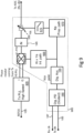
- FIG. 6A illustrates a generalized clock circuit 695 employing dual reference clock inputs to provide high order phase tracking for jitter rejection/cancellation and clock recovery implementations.
- high order phase tracking clock circuit 695 is employed in the feedback loop of PLL device 100 indirectly controlling the VCO 140.
- Copy 187 of the output signal 180 of the PLL device 100 is compared with a second reference clock signal 605 at a digital phase detector 160.
- phase differences detected by digital phase detector 160 are provided to digital accumulator 165.
- digital accumulator 165 performs numerical integration; wherein integration of frequency results in phase information, providing a control signal 651.
- control signal 651 is an alternating current (AC) signal wherein the mean value characteristic (also referred to as the DC component) indicates a frequency difference between a copy of output signal 187 (at least initially more synchronized to the reference clock signal 105) and reference clock signal 605. Oscillating characteristics of AC control signal 651 are indicative of dynamic jitter between reference clock signal 605 and the copy of output signal 187.
- phase information can be encoded in a digital signal 651 which may include a bit pattern corresponding to at least one phase difference detected within a time window. Details of bit pattern encoding for digital signal 651 can be similar to description hereinabove with respect to controls signals 151. 251, 353, etc.
- a copy of control signal 651 is provided to drive a digitally controlled delay locked loop (DLL) component or a component capable of introducing 2Pi rotations in the feedback signal 246 in the feedback path of the PLL device 100.
- DLL delay locked loop
- a second digital accumulator 665 for example of "Ki x 1/s" type, performs a second numerical integration providing control signal 151 for driving phase rotator 115 for example as described hereinabove.
- This integral control feedback control loop nested within the feedback loop of PLL device 100 is employed for slow frequency compensation which over time (over multiple signal feedback loop cycles) preferentially identifies the center frequency of reference clock signal 605 and, through the feedback loop of the PLL device 100, indirectly adjusts the oscillation frequency of the VCO 140 to match the frequency of reference clock signal 605.
- components in this integral feedback control path are not perfect, some residual non-linearities can be corrected by optionally employing look up table (LUT) component 270.
- the integral control feedback control provides filtered feedback signal 655 which can have remaining low-frequency jitter (spurs) for example originating from the operation of the phase rotator 115.
- control signal 651 is provided to a "Kp" component 670, for example a digital gain block such as a multiplier, which outputs digital control signal 653.
- Digital control signal 653 is employed to drive fine delay element 350.
- digital control signal 653 can include a digital bit pattern.
- Delay element 350 is employed to provide phase non-linearity correction by advancing or retarding a (raising or falling) transition of filtered signal 655, in time, to provide filtered feedback signal 656 to the PLL device 100, for example to (analog) phase detector 110.
- the phase non-linearity correction provides the proportional control.
- fine delay element 350 can include an analog device wherein an analog anti-imaging filter 675 (shown in dashed outline), for example a DAC converts digital signal 653 into an analog drive signal to drive such an analog fine delay element 350.
- an analog anti-imaging filter 675 shown in dashed outline
- a DAC converts digital signal 653 into an analog drive signal to drive such an analog fine delay element 350.
- Specific implementations can employ a voltage controlled fine/linear delay element 350 having a resolution of about 20fs and a range of about 5ps.
- filtered signal 655 being provided as an input to fine delay element 350, residual non-linearity from the control path can be corrected via the fine proportional control path by applying a high-pass transfer function attenuating low frequency spurs.
- employing a single digital phase detector 160 for both the integral and proportional phase control paths reduces implementation area and power requirements in a component employing clock circuit 695.
- the 2nd order phase tracking loop operation of clock circuit 695 in the phase domain is illustrated with reference to Figure 6B .
- the method and apparatus employ digital accumulator 165 to mimic a VCO pole in the phase domain.
- the emulated VCO (165) is modelled as an integrator block "1/s" performing integration in the phase domain.
- the control signal path splits to provide segmented controls: an integral control signal path using digital accumulator 665 (driving the phase rotator 115), and a fine proportional control path using digital filter (Kp) 670 (driving fine resolution digitally controlled delay element 350).
- Kp digital filter
- the cascading of the phase rotator 115 with the fine delay element 350 illustrated in Figure 6A performs intrinsic summation "+" in the phase domain.
- digital filter Kp 670 indirectly controls the VCO 140 to dynamically remove (attenuate) spurs caused by non-linearities of the phase rotator (i.e. tracking the AC around the jitter mean).
- Figure 6C illustrates a method 600 of signal processing in clock circuit 695 in accordance with the proposed solution. Specifically, one or more steps in Figure 6C may be performed by one or more components as described in Figure 6A with reference to Figure 6B . While the various steps in this flowchart are introduced and described sequentially, one of ordinary skill in the art will appreciate that some or all of the steps may be executed in different orders, may be combined or omitted, and some or all of the steps may be executed in parallel. Furthermore, the steps may be performed actively or passively.
- Integration in the phase domain is performed 610 on detected phase differences between reference clock signal 605 and output signal copy 187 from PLL device 100 to provide control signal 651.
- a static offset of the VCO 140 is adjusted 620 indirectly to change the oscillation frequency of VCO 140 to match the frequency of reference clock signal 605.
- Control signal 651 is (digitally) filtered 630 to indirectly adjust a dynamic offset of the VCO 140 to correct the oscillation of VCO 140 to provide phase non-linearity correction.
- Summing 640 oscillation frequency adjustments attenuates oscillation frequency components in the oscillation of VCO 140 to provide phase non-linearity correction.
- the former is controlled via the integral control path to remove steady state error (second order loop characteristics) and the latter is controlled via the proportional control path (phase control which dominates the bandwidth of the overall PLL feedback control loop) to track instantaneous phase dithering.
- the proportional PLL feedback control path addresses (corrects/fixes) shortcomings of the integral PLL feedback control path.
- the circuit template of clock circuit 695 illustrated in Figure 6A can be employed to act as a PLL jitter cleaner, (preferably to act as a PLL jitter canceler) for clock generation implementations.
- transmitter component implementations employ clock generation.
- clock generation implementations can be used to drive clock trees (not shown).
- clock circuit 695 template generically illustrated in Figure 6A is employed for clock generation in a transmitter component with the objective to reduce/suppress jitter in VCO 140.
- a copy reference clock signal 105 to the digital phase detector 160 as the second reference clock signal 605
- high order jitter suppression in the VCO output signal 180 can be provided.
- the 2nd order phase control provided by clock circuit 695 described hereinabove follows (tracking) clean reference clock 105 to reduce jitter at the VCO output 180.
- the combination of the PLL device 100 and clock circuit 695 operates as a digital VCO with segmented proportional and integral controls in a 2 nd order phase control loop to provide clock generation.
- synchronized output signal 180 is illustrated to be employed (fed) to provide cadence to (drive) a DAC in a transmitter implementation (similar to illustration in Figure 2A ), in other applications (not illustrated) the synchronized output signal 180 can be employed to drive a clock tree.
- clock circuit 695 template generically illustrated in Figure 6A is employed for clock recovery in a receiver component with the objective to track a remote transmitter clock signal as received.
- the received signal 185 typically a copy of the remote transmitter clock signal derived from the received signal
- the digital phase detector 160 as the second reference clock signal 605
- the jitter profile of the local VCO 140 can be adjusted to follow the jitter profile of the remote transmitter as detected over the link regardless of signal imperfections.
- the output signal 180 synchronized to the remote transmitter clock signal 185, is employed to drive an ADC in a receiver implementation (similar to illustration in Figure 2B ) with the objective for the jitter profile of the local ADC VCO 140 to match the jitter profile of the received signal 185.
- clock circuit 695 employing clock circuit 695 in a receiver, high order clock recovery is provided by improved tracking of the remote (foreign) transmitter clock.
- the 2nd order phase control provided by clock circuit 695 described hereinabove follows (tracking) departures of remote (foreign) transmitter clock from ideal ( Figure 1B and accompanying description).
- the combination of the PLL device 100 and clock circuit 695 operates as a digital VCO with segmented proportional and integral controls in a 2 nd order phase control loop to provide clock extraction.
- the jitter in the local receiver clock is determined by the jitter properties of remote transmitter PLL (as detected locally from the received signal 185) and the jitter properties of the local receiver PLL (imperfect components).
- the remote and local jitter contributions can be addressed independently to achieve the best jitter reduction/suppression performance of the overall link.
- the local receiver clock circuit 695 will track the transmitter clock as received and will further attenuate local receiver's clock intrinsic jitter to account for imperfect components in the local PLL loop.
- the fine resolution delay element used in the proportional control path also rejects (attenuates) low-frequency jitter (spurs) originating from the phase rotator (because the phase rotator follows a high-pass transfer function with respect to the clock recovery function) used in the integral control path.
- the transmitter clock signal is an extracted clock signal from a SerDes link.
- the SerDes system is a PISO (Parallel Input, Serial Output) system that can include a parallel clock input, various data input lines, and various input data latches.
- the SerDes system may use an internal or external PLL device to multiply the incoming parallel clock up to a specific frequency.
- the SerDes system is a SIPO (Serial Input, Parallel Output) system.
- the receiver clock signal can be recovered from data obtained using a serial clock recovery technique as described herein.
- a receiver employing a single digital phase detector 160 in accordance with the proposed solution benefits from advantages of low power and low jitter clock recovery implementations which are insensitive to ppm differences between the remote transmitter and local receiver clocks.
- employing 2 nd order clock recovery methods proposed herein wherein a ppm difference exists between the transmitter clock 185 and receiver reference clock signal 105, reduces the phase error of output signal 180 close to '0' regardless of the ppm difference.
- Such a ppm offset would generate in-band spurs from the operation of phase rotator 115 in the clock recovery loop.
- the frequency response in terms of noise added by the phase rotator output through to the DPLL output 655 is bandpass (see proportional phase control path description hereinabove), and no poles of the closed loop phase control lie outside the unit circle in the complex plane. This confirms system stability.
- the proposed clock circuits, components and signal processing methods when implemented particularly, but not exclusively, in receiver components provide improved clock recovery performance which can also be understood as reducing a likelihood of cycle slips during clock extraction when compared to conventional clock extraction ( Figure 2B ).
- Such reduced likelihood of cycle slips improves tolerance of ppm differences between transmitter and receiver clocks, improved tolerance which is reflected in reduced signal-to-noise ratio (SNR) with respect to a received signal.
- SNR signal-to-noise ratio
- the clock circuits, receiver components and signal processing methods proposed herein provide an ADC with sampling clock signals having reduced jitter improving overall SNDR of data converters.
- the proposed clock circuits, components and signal processing methods presented herein provide a very small controllable clock recovery bandwidth when compared to conventional schemes.
- the fine clock recovery bandwidth control provided herein has high potential in flex-grid/grid-less system (liquid spectrum) applications as the clock recovery band (the outer band of a channel signal spectrum) is desensitized to adjacent channel energy (robust to neighboring channel interference). This advantage is twofold: it allows for more compact channel spacing, and reduces both clock jitter and overall bit error rate. In turn, these advantages can potentially enable richer and/or higher modulation formats to be employed over communications links.
- Embodiments may be implemented in a clock circuit of a computing system. Any combination of mobile, desktop, server, router, switch, embedded device, or other types of hardware may employ such a clock circuit.
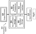
- the computing system 800 may include one or more computer processors 802, non-persistent storage 804 (e.g., volatile memory, such as random access memory (RAM), cache memory), persistent storage 806 (e.g., a hard disk, an optical drive such as a compact disk (CD) drive or digital versatile disk (DVD) drive, a flash memory, etc.), a communication interface 812 (e.g., Bluetooth interface, infrared interface, network interface, optical interface, etc.), and numerous other elements and functionalities.
- non-persistent storage 804 e.g., volatile memory, such as random access memory (RAM), cache memory
- persistent storage 806 e.g., a hard disk, an optical drive such as a compact disk (CD) drive or digital versatile disk (DVD) drive, a flash memory, etc.
- the computer processor(s) 802 may be an integrated circuit for processing instructions.
- the computer processor(s) may be one or more cores or micro-cores of a processor.
- the computing system 800 may also include one or more input devices 810, such as a touchscreen, keyboard, mouse, microphone, touchpad, electronic pen, or any other type of input device.
- the communication interface 812 may include an integrated circuit for connecting the computing system 800 to a network (not shown) (e.g., a local area network (LAN), a wide area network (WAN) such as the Internet, mobile network, or any other type of network) and/or to another device, such as another computing device.
- a network not shown
- LAN local area network
- WAN wide area network
- mobile network or any other type of network
- the computing system 800 may include one or more output devices 808, such as a screen (e.g., a liquid crystal display (LCD), a plasma display, touchscreen, cathode ray tube (CRT) monitor, projector, or other display device), a printer, external storage, or any other output device.
- a screen e.g., a liquid crystal display (LCD), a plasma display, touchscreen, cathode ray tube (CRT) monitor, projector, or other display device
- One or more of the output devices may be the same or different from the input device(s).
- the input and output device(s) may be locally or remotely connected to the computer processor(s) 802, non-persistent storage 804, and persistent storage 806.
- Software/firmware instructions in the form of computer readable program code to perform embodiments of the invention may be stored, in whole or in part, temporarily or permanently, on a non-transitory computer readable medium such as a CD, DVD, storage device, a diskette, a tape, flash memory, physical memory, or any other computer readable storage medium.
- the software/firmware instructions may correspond to computer readable program code that, when executed by a processor(s), is configured to perform one or more embodiments of the proposed solution.
- state machine logic may implement and/or include such and/or other instructions for implementing and/or may be configured to perform one or more embodiments of the proposed solution.
- the computing system or group of computing systems described in Figure 8 may include functionality to perform a variety of operations disclosed herein.
- the computing system(s) may perform communication between processes on the same or different systems.
- a variety of mechanisms, employing some form of active or passive communication, may facilitate the exchange of data between processes on the same device. Examples representative of these inter-process communications include, but are not limited to, the implementation of a file, a signal, a socket, a message queue, a pipeline, a semaphore, shared memory, message passing, and a memory-mapped file.
- sockets may serve as interfaces or communication channel end-points enabling bidirectional data transfer between processes on the same device.
- a server process e.g., a process that provides data
- the server process may create a first socket object.
- the server process binds the first socket object, thereby associating the first socket object with a unique name and/or address.
- the server process then waits and listens for incoming connection requests from one or more client processes (e.g., processes that seek data).
- client processes e.g., processes that seek data
- the server process Upon receiving a data request, the server process analyzes the request and gathers the requested data. Finally, the server process then generates a reply including at least the requested data and transmits the reply to the client process.
- the data may be transferred, more commonly, as datagrams or a stream of characters (e.g., bytes, bits, symbols, etc.)
- Shared memory refers to the allocation of virtual memory space in order to substantiate a mechanism for which data may be communicated and/or accessed by multiple processes. Other techniques may be used to share data, such as various data described in the present application, between processes without departing from the scope of the proposed solution.
- the processes may be part of the same or different application and may execute on the same or different computing system.
- FIG. 9 is a schematic circuit diagram of a clock recovery circuit using segmented proportional/integral control and a digital VCO emulator with no Rx PLL in accordance with the proposed solution.
- a clock recovery circuit 900 of Figure 9 provides similar functionality as the clock circuit 695 in Figures 6 and 7 without the PLL device 100. Instead, the reference clock 105 is provided to a Tx PLL circuit 905 which connects to the phase rotator 115.
- the clock recovery circuit 900 includes the digital phase detector 160, the digital accumulator 165, the digital accumulator 665, and the feedback divider 145. Additionally, the clock recovery circuit 900 includes the digital filter (Kp) 670 driving fine resolution digitally controlled delay element 350 on the receiver clock signal 187.
- Kp digital filter
- the removal of the PLL device 100 provides lower power and smaller footprint, relative to the embodiments of Figures 6 and 7 , but the frequency of the receiver clock signal 187 sent to the ADC is at most Fs/4.
Landscapes
- Stabilization Of Oscillater, Synchronisation, Frequency Synthesizers (AREA)
Abstract
Description
- A phase locked loop (PLL) is employed to produce a synchronized clock signal that has a phase matched with that of a reference clock signal, typically the synchronized clock signal has a higher frequency than the frequency of the reference clock signal. The reference clock signal can be provided by an onboard reference clock coupled to a PLL device. Alternatively to using an onboard reference clock, the synchronized clock signal can be matched to the phase of source clock information obtained through synchronous Ethernet (SyncE), or from a precision time protocol (PTP), such as a protocol based on the IEEE 1588 standard.
- Typically, the synchronized clock signal can be used to drive various operations performed by apparatus providing receive/transmit or input/output data transfers, for example in a transceiver or in a serializer-deserializer (SerDes) input/output component in a digital system. Examples of the transceiver include an optical transceiver, a wireless transceiver, etc.
- For example, in a transmit direction, such a synchronized clock signal provided by a PLL device can be used to drive a Digital to Analog Converter (DAC) to send digital data over a link. The PLL device is said to be used for clock generation and the synchronized clock signal is said to provide a transmitter clock signal.
- Conversely, in the receive direction, such a synchronized clock signal provided by a PLL device can be used to drive an Analog to Digital Converter (ADC) to sample an input signal received over a link (electrical connection, optical cable, wireless Radio Frequency beam, etc.) In the receive direction, the synchronized clock signal needs to be phase matched and frequency matched to a transmitter clock signal as received at a local receiver as part of the input signal received. The PLL device in such a receiver is said to be used for clock extraction and the synchronized clock signal is said to provide a receiver clock signal.
- Clock generation can also be used to drive clock trees for example.
- In general, an analog phase locked loop (PLL) device includes a voltage-controlled oscillator (VCO) component that generates a VCO output signal which is signal processed to provide the synchronized clock signal based on the reference clock signal.
-
Figure 1A illustrates ageneric PLL device 100. Areference clock signal 105 can include a voltage signal from an onboard or external reference clock source (not shown) to which the phase of the synchronizedclock signal 180 of thePLL device 100 is intended to lock to. The reference clock source can be software and/or hardware, such as an integrated circuit, that includes functionality for generating and/or providing timing information to thePLL device 100. For example, a hardware reference clock source can include a crystal oscillator or a global position system (GPS) receiver. Software examples of reference clock sources include an implementation of a network protocol over a communications network for synchronizing clocks, such as synchronous Ethernet (SyncE), or an implementation of a precision time protocol (PTP) for example compliant to the IEEE 1588 standard. - The
analog PLL device 100 operates in a signal processing loop which progressively, over a number of loop cycles, adjusts the VCO output signal to provide the synchronized clock signal. The signal processing loop of thePLL device 100 includes ananalog phase detector 110 employed to extract a difference between afeedback copy 247 of aVCO output signal 180 and thereference clock signal 105. While ananalog phase detector 110 is shown inside thePLL device 100 inFigure 1 , in other implementations an analog phase-frequency detector can be used instead. A phase-frequency detector inside thePLL device 100 can produce two signals that correspond to the phase difference and a frequency difference rather than a single phase difference signal. In other implementations, a digital phase detector can be used instead of theanalog phase detector 110 with due changes in the operation of thePLL device 100 and feedback loop. - A feedback divider includes hardware, such as an integrated circuit, having functionality to divide the frequency of an input signal by an N-multiple. In the feedback loop of
PLL device 100, the input signal of thefeedback divider 145 isoutput signal 180 and such division by thefeedback divider 145 produces acorresponding feedback signal 247 which is a copy of theoutput signal 180 at a lower frequency. For example, thePLL device 100, and particularly theVCO 140, multiplies thereference signal 105 by an N-multiplier to generate theoutput signal 180. In the feedback loop of thePLL device 100,feedback divider 145 accounts for the increased frequency of theoutput signal 180 in order to returnfeedback signal 247 as an input to theanalog phase detector 110 at a similar frequency as that ofreference signal 105. Optionally, acascaded feedback divider 147 is illustrated to further divide the frequency in feedback loop by another M-multiple. - The
PLL device 100 also includes acharge pump 120, aloop filter 130 and various other PLL components (some shown in more detail below). A feedback signal path between the output of theVCO 140 and theanalog phase detector 110 can include one ormore feedback dividers - For example, the
charge pump 120 includes hardware that provides functionality to generate a current signal from a voltage signal, e.g., a current signal that relates to the phase difference (and the frequency difference) detected by theanalog phase detector 110. - The
loop filter 130 includes hardware having functionality to check stability within thePLL device 100 as well to operate as a frequency bandwidth limiter to synchronize theoutput signal 180 with thereference signal 105. For example,loop filter 130 includes a low pass filter that operates according to a current signal produced by thecharge pump 120 to output a signal. In this sense, theanalog PLL device 100 synchronizes to the reference clock signal with a high bandwidth to reduce (VCO) phase noise. - The voltage-controlled
oscillator device 140 includes hardware having functionality to generate an oscillating signal (180) typically at a higher frequency than that of thereference clock signal 105. For example, the voltage-controlledoscillator device 140 can include functionality to obtain the signal from theloop filter 130 to generate theoutput signal 180 with a predefined period and frequency. - A person of skill in the art would understand that signal processing functionality of
PLL device 100 operating in a loop can have startup characteristics and steady state characteristics. ThePLL device 100 can provide a lock signal output by steady-state detector 157 indicative of startup (unsettled, unlocked) and steady-state (settled, locked) operation. The steady-state detector 157 can be hardware and/or software that includes functionality to determine whether theoutput signal 180 is in a steady-state mode. In the steady-state mode, the phase (and frequency) of theoutput signal 180 may be locked to thereference signal 105. For example, an amount of phase error and/or frequency error may have converged to a (local) minimum where theoutput signal 180 is approximately phase matched and frequency fixed with respect to thereference signal 105. Conversely, when thePLL device 100 is in a transient mode, thePLL device 100 may be adjusting the phase and/or frequency of theoutput signal 180 to match thereference signal 105. Typically, in transient mode the oscillator of theVCO 140 may have just been turned on and may not have settled yet. - In some applications, the
PLL device 100 is used for clock generation. In other applications,output signal 180 can be an extracted clock signal obtained using thereference signal 105. Regardless of clock generation/extraction application, theVCO 140 is not a perfect oscillator and other elements in the PLL loop of thePLL device 100 are not perfect in their operation either. As described herein above, the feedback path is used to provide information from theoutput 180 of thePLL device 100, typically acopy 247 of theoutput signal 180, back to the input of thePLL device 100 for comparison with thereference clock signal 105 repeatedly in a loop. - In clock generation applications it is desired for the
output signal 180 to be ideal in the sense of having a fixed frequency locked to the phase of thereference clock signal 105. In practice however, theoutput signal 180 has departures from an ideal waveform, departures which are referred throughout herein as jitter. Feedback control is employed to reduce/suppress and preferably reject/canceljitter in the PLL loop. In clock extraction applications it is desired for theoutput signal 180 to track the remote transmitter clock. Feedback control is employed in order to follow the remote transmitter clock to reduce/suppress and preferably reject/cancel dynamic jitter between the remote transmitter clock (as received) and theoutput signal 180. -
Figure 1B schematically illustrates an example of a timing diagram of theoutput signal 180 obtained during phase locked operation of thePLL device 100. As shown inFigure 1B , a generated output signal 640 (output signal 180) is compared with a desired ideal (output)signal 630 along a time axis and another axis for example with respect to voltage. It is important to note that the desiredideal signal 630 is not a physical signal in an I/O or transceiver apparatus, and thereference clock signal 105 typically has lower frequency than theideal signal 630. Thus, while theideal signal period 630 is constant, for various periods the generatedoutput signal 640 may deviate from theideal signal period 630. Such deviations may be the result of PLL noise introduced by one or more components in a PLL device, for example the generatedoutput signal 640 includes various amounts of PLL noise i.e.,jitter 611,jitter 612,jitter 613, jitter 614 identifying departures of the generatedoutput signal 640 from theideal signal period 630. While time-interval error jitter is shown byjitter 611,jitter 612,jitter 613, and/or jitter 614, other types of jitter may also exist in the generatedoutput signal 640, such as cycle-to-cycle period jitter, long term jitter, phase jitter, and any other forms of phase noise. -
Figure 2A illustrates a block diagram of a transmitter apparatus. As shown inFigure 2A , aclock circuit 295 includesPLL device 100 providing clock generation.Clock circuit 295 can be a portion of an I/O or a transceiver apparatus that includes hardware and/or software for transmitting a clock signal within the same or to another computing device.Output signal 180 of thePLL device 100 is employed to provide cadence to a digital-to-analog converter (DAC) which includes hardware and/or software to output digital data as an output signal TxSignalOut for transmission over a link. Alternatively to use in a transmitter,output signal 180 ofclock circuit 295 can be used to drive (not shown) a clock tree (without the use of a DAC). Assuming that thereference clock 105 is ideal, the PLL jitter (Figure 1B ) ofclock circuit 295 can be regarded as clock generation jitter. - With reference to
Figure 2B , aVCO 140 is used in a PLL loop for data signal extraction at a local receiver. For successful data signal extraction, the data clock of the local receiver at the near end of the link needs to follow the data clock of the remote transmitter at the far end of the link. The input signal received from the remote transmitter includes both data sent and a transmitter clock signal of the remote transmitter; thePLL device 100 is employed to extract the transmitter clock signal from the input signal. - In the receiver apparatus schematically illustrated in
Figure 2B , theoutput signal 180 of theVCO device 140 is employed to provide cadence to an analog-to-digital converter ADC which includes hardware and/or software to convert the received input signal to a digital data output signal providing data extraction from the received input signal. It is desired for theoutput signal 180 of thePLL device 100 to have a frequency matched to the frequency of the received input signal and phase locked to the phase of the received input signal. In practice however theoutput signal 180 has departures from the received input signal, departures which are referred herein as clock recovery jitter. - The data clock of the remote transmitter can be, and typically is, noisy including transmitter jitter for example as described hereinabove. It is emphasized that any transmitter data clock signal, ideal (theoretical) or noisy (practical), can only be seen at the local receiver through the physical link between the remote transmitter and the local receiver, physical link which itself is noisy. A simplification herein is that the local receiver cannot distinguish between remote transmitter jitter and link jitter.
- A common way of implementing clock recovery in a receiver is by directly controlling the
VCO 140 through a proportional/integral controller in a manner summarily illustrated inFigure 2B . Notably, in the prior art theVCO 140 is controlled directly. A digital phase detector 210 (typically Godard type) extracts the transmitter clock from the received input signal and the output of thedigital phase detector 210 is used by a proportional/integral controller 222 to adjust thereceiver VCO 140 directly. - A person of ordinary skill in the art would understand that there is a loop delay associated with the transmitter clock phase extraction. As the signal path in the PLL loop includes a high pass filter in the forward signal path (from VCO to output) and low pass filter in the feedback signal path (from
data clock 185 to output), a 3dB cutoff point needs to be increased for successful operation which leads to excessive peaking.Figure 2C illustrates peaking in the clock recovery provided by prior art attempts such as illustrated inFigure 2B . Excessive signal processing delay in the loop limits clock recovery bandwidth. The achievable bandwidth of such a clock recovery loop needs to be limited to a low value to avoid excessive peaking. Limiting clock recovery bandwidth directly affects the overall jitter rejection in the PLL loop since a small bandwidth limits the amount of VCO phase noise suppression which follows a high-pass transfer function. - Accordingly, depending on application, known prior art solutions limitations include: lower performance, larger die area, higher power consumption, worst jitter performance in terms of clock recovery (signal tracking). There is a need in applications employing clock circuits reduce/suppress and ultimately reject jitter.
- One aspect of the solution proposed herein includes emulating a VCO as part of a digital control loop. Another aspect of the proposed solution proposed herein includes splitting feedback loop control in two. In accordance with the proposed solution, a method for operating a clock circuit is presented which emulates digitally the operation of a VCO with a digital accumulator followed by segmented controls providing proportional and integral loop control functions. A combination of a phase rotator and an accumulator is employed to perform frequency tracking (integral path) and a fine digitally controlled delay element is employed to perform the phase tracking (proportional path).
- In general, in accordance with an aspect of the proposed solution embodiments employ apparatus including a phased locked loop (PLL) device having a first reference clock signal and a signal processing system coupled to the PLL device. The signal processing system obtains an output signal from the PLL device. The signal processing system further determines, using a digital phase detector operating on a copy of the output signal and second reference clock signal clock signal to determine an amount of phase difference between the output signal and second reference clock signal. The processing system employs the digital phase detector and a digital accumulator to combine multiple phased differences in an integration window (integral path) to filter, using a phase rotator, a portion of the amount of phase difference from the output signal to generate a filtered signal. In accordance with another aspect, the embodiments employ a digitally controlled fine delay element to provide additional signal filtering (proportional path) in the feedback loop of the PLL device. The output of the same digital phase detector is also employed to control the delay element. Clock circuit implementations in which the second reference clock signal is a copy of the first reference clock signal can provide clock generation in a transmitter. Clock circuit implementations in which the second reference clock signal is a transmitter clock signal received from a remote transmitter provide clock extraction in a receiver.
- In the following detailed description of various embodiments numerous specific details are set forth in order to provide a more thorough understanding of the proposed solution. However, it will be apparent to one of ordinary skill in the art that the invention may be practiced without these specific details. Well-known features have not been described in detail to avoid unnecessarily complicating the description.
- Specific embodiments of the invention will now be described in detail with reference to the accompanying figures. Like elements in the various figures are denoted by like reference numerals.
- Throughout the application, ordinal numbers (e.g., first, second, third, etc.) may be used as an adjective for an element (i.e., any noun in the application). The use of ordinal numbers is not to imply or create any particular ordering of the elements nor to limit any element to being only a single element unless expressly disclosed, such as by the use of the terms "before", "after", "single", and other such terminology. Rather, the use of ordinal numbers is to distinguish between the elements. By way of an example, a first element is distinct from a second element, and the first element may encompass more than one element and succeed (or precede) the second element in an ordering of elements.
- Other aspects of the invention will be apparent from the following description and the appended claims.
-
-
Figure 1A is a schematic circuit diagram illustrating a generic PLL loop; -
Figure 1B shows an example of a timing diagram illustrating PLL jitter in a PLL loop; -
Figure 2A is a schematic circuit diagram illustrating a simplified transmitter of prior art -
Figure 2B is a schematic circuit diagram illustrating a simplified prior art receiver; -
Figure 2C includes schematic plots illustrating excessive peaking in prior art receivers; -
Figure 3A is a schematic circuit diagram of a clock recovery circuit in a receiver in accordance with the proposed solution; -
Figure 3B is a schematic circuit diagram of another clock recovery circuit in a receiver in accordance with the proposed solution; -
Figure 4 is a schematic circuit diagram of a clock recovery circuit in a transmitter in accordance with the proposed solution; -
Figure 5 is a schematic circuit diagram of a clock recovery circuit showing decoupling between clock recovery and jitter cancellation; -
Figure 6A is a schematic circuit diagram of a generic clock recovery circuit showing decoupling between clock recovery and jitter cancellation in accordance with the proposed solution; -
Figure 6B is a schematic signal processing diagram of a generic clock recovery circuit showing decoupling between clock recovery/generation and jitter cancellation in accordance with the proposed solution; -
Figure 6C is a schematic flowchart of a method of signal processing in accordance with one or more embodiments; -
Figure 7A is a schematic circuit diagram of the generic clock circuit employed in a transmitter providing clock generation and jitter cancellation in accordance with the proposed solution; -
Figure 7B is a schematic circuit diagram of the generic clock circuit employed in a receiver providing clock extraction/recovery and jitter cancellation in accordance with the proposed solution; -
Figure 8 illustrates a computing system in accordance with one or more embodiments; and -
Figure 9 is a schematic circuit diagram of a clock recovery circuit using segmented proportional/integral control and a digital VCO emulator with no Rx PLL in accordance with the proposed solution. - Embodiments of the proposed solution provide systems, apparatus, clock circuits and signal processing methods indirectly controlling VCO of a PLL device via a feedback path in a PLL loop.
- Some embodiments of the proposed solution relate to a system, apparatus, and a method for clock recovery at a receiver. With reference to
Figure 3A , one or more implementations are directed to aclock recovery circuit 395 which includes aphase rotator 115 disposed within the feedback loop of a phase locked loop (PLL)device 100. Adigital phase detector 160 coupled to thephase rotator 115 is employed to determine a frequency offset and/or phase misalignment between atransmitter clock signal 185, as received at the receiver, and acopy 187 of theoutput signal 180 of thePLL device 100. Theclock circuit 395 providesoutput signal 180, the synchronized output signal, as a receiver clock signal (187) to an ADC. - A
phase rotator 115 is configured to apply a phase shift correction in the feedback loop to reduce the frequency offset and/or phase misalignment between thetransmitter clock signal 185 and thereceiver clock signal 187. Thephase rotator 115 provides filteredsignal 155 as the feedback signal to thePLL device 100. - Specifically, the
PLL device 100 includesanalog phase detector 110, for example an integrated circuit including functionality to determine a difference in phase between two input signals e.g.,reference clock signal 105 and filteredsignal 155 fed back from theVCO 140 output. The phase rotator based digital clock recovery provided allows theclock circuit 395 to lock to a locally received data signal generated by a remote transmitter PLL locked to a reference clock different from the reference clock (105) of thereceiver PLL device 100. - The
digital phase detector 160 is employed in theclock circuit 395 to provide clock recovery in a receiver. Thedigital phase detector 160 includes hardware and/or software that implements functionality to determine an amount of phase difference betweentransmitter clock signal 185 and thereceiver clock signal 187 which is a feedback copy ofoutput signal 180. The clock circuit further includes adigital accumulator 165 coupled to thedigital phase detector 160. Thephase rotator 115 and thedigital accumulator 165, using the amount of phase difference between thetransmitter clock signal 185 and the receiver clock signal 187 (output signal 180), filter a portion of the amount of phase difference from anothercopy 246 of the output signal 180 (feedback divider not shown) to generate afiltered signal 155 which is provided to theanalog phase detector 110. - The signal path including the
receiver clock signal 187 provided from thePLL device 100 to thedigital phase detector 160, thedigital phase detector 160,digital accumulator 165,phase rotator 115 and the filteredsignal 155 provided as an input theanalog phase detector 110 of thePLL device 100, implements a phase rotator digital PLL nested in the feedback loop of theanalog PLL 100. The phase rotator digital PLL locks to thetransmitter clock signal 185. As mentioned with reference toFigure 2B above, it is noted that thetransmitter clock signal 185 is embedded with the data signal in the signal received over the link. This configuration ofclock circuit 395 decouples the high bandwidth requirement of theanalog PLL 100 to reject the phase noise of theVCO 140 from the requirement of the clock recovery bandwidth of the phase rotator digital PLL. The phase rotator based digital clock recovery bandwidth is selected to balance jitter tracking with respect to thetransmitter clock signal 185 as received vs. jitter rejection of the VCO/PLL jitter. - It is noted that the
digital phase detector 160 itself is not a perfect device. In accordance with the proposed solution, digital phase detector error can be reduced through averaging, or integration, the result being understood to provide integral control. - In particular,
phase rotator 115 includes hardware providing functionality to adjust a frequency offset and/or phase misalignment betweentransmitter clock signal 185 and a receiver clock signal 187 (a copy of output signal 180). As such,phase rotator 115 includes one or more hardware components that include functionality to apply a predetermined amount of phase shift tofeedback copy 246 ofoutput signal 180 based oncontrol signal 151. - In an implementation a phase rotator includes a pair of variable gain amplifiers that apply predetermined weights to an in-phase (I) component and a quadrature (Q) component of an input signal, a feedback copy of
output signal 180. For example, a phase rotator is configured to generate a pair of differential phase signals from its input signal that correspond to the I component (i.e., "I phase signal") and the Q component (i.e., "Q phase signal") of the input signal. In one or more embodiments, for example, the I phase signal and the Q phase signal are expressed using the following equations:

where A is the amplitude of an output signal from thephase rotator 115, such asfiltered signal 155; k is a gain value in the phase rotator, v(t) is the voltage of the input signal, t is the time domain, ϕ is the phase shift applied to feedback signal 246 (output signal 180) by thephase rotator 115. The I phase signal and/or the Q phase signal may be generated within thephase rotator 115 for example by a resistor-capacitor (RC) polyphase network, frequency dividers, and/or a resistor-capacitor pairs. Furthermore, thephase rotator 115 can include an interpolator circuit that generates a linear summation of the I phase signal and the Q phase signal. Thephase rotator 115 produces filteredsignal 155 with the applied phase shift as its output signal. - Keeping with
Figure 3A , in one or more implementations, the ϕ phase shift of thephase rotator 115 is determined by acontrol signal 151. For example, thecontrol signal 151 includes a binary signal provided by a multi-bit register that includes functionality to instruct thephase rotator 115 to produce no phase shift or one or more steps of phase shift. More generically, the binary signal includes a bit sequence which determines which step of phase shift is produced by the phase rotator 115 (e.g., '101' corresponds to one amount of phase shift and '001' corresponds to a different amount of phase shift). Furthermore, thephase rotator 115 can be a single-step device, e.g., a single amount of phase shift based on thecontrol signal 151. On the other hand, thephase rotator 115 can be a multi-step device. In a multi-step device, thephase rotator 115 can produce different amounts of phase shift based on acontrol signal 151. In one or more implementations, for example, thephase rotator 115 produces an approximate phase shift of 100 femtoseconds per step. If thecontrol signal 151 corresponds to two steps, then the phase rotator may produce 200 femtoseconds of phase shift to output signal 180 orfeedback copy 246 ofoutput signal 180. - In one or more implementations, the
control signal 151 for aphase rotator 115 is based on a frequency offset and/or phase misalignment, typically averages thereof, between atransmitter clock signal 185 and an extracted receiver clock signal 187 (180). As noted above thetransmitter clock signal 185 is embedded in the signal received over the link. For example, thetransmitter clock signal 185 can be obtained using a Godard extraction algorithm. By way of a more specific example, thedigital phase detector 160 includes a Godard digital phase detector that implements the Godard extraction algorithm. For example, in an optical transceiver, thetransmitter clock signal 185 can be extracted from the "out-of-band" spectrum of the received signal by applying the Godard phase extraction process on the "out-of-band" frequency spectrum, i.e., in Godard bins of the upper sideband and lower sideband of the frequency spectrum of the received signal. For more information on extracting thetransmitter clock signal 185 received within a signal spectrum, see D. Godard, "Passband Timing Recovery in an All-Digital Modem Receiver," IEEE Trans. On Communications, Vol. 26, Issue:5, May 1978. While applying a Godard extraction algorithm is one example for obtaining thetransmitter clock signal 185, other timing recovery methods of transmitter clock signals 185 are also contemplated, such as a Gardner timing recovery method. Additional aspects of transmitter clock signal extraction from an input signal are presented in co-pending commonly assignedUS Patent Application Ser. No. 15/795,676, filed 10/27/2017 - For example, the
control signal 151 provided to phaserotator 115 can be generated by adigital accumulator 165 based on multiple differences provided by thedigital phase detector 160. Thedigital accumulator 165 can include hardware and/or software which provides functionality to store a value of at least one phase difference, for example, in a hardware register. In one or more implementations, thedigital accumulator 165 is an integrated circuit which also includes functionality to store various measurements of the difference between atransmitter clock signal 185 and a receiver clock signal 187 (180). - The number of phase differences stored in a time window, averaging of phase differences within the time window, weighting based on phase difference measurements, and phase step selection for the
phase rotator 115 to apply can amount to the corresponding integral control provided viacontrol signal 151. - While employing the
phase rotator 115 of the proposed solution has been described with respect to clock recovery, the apparatus,clock circuit 395 and signal processing method can also be employed for clock generation to reduce VCO/PLL jitter (not shown) wherein the transmittedclock signal 185 illustrated inFigure 3A is replaced by a copy ofreference clock signal 105. - Notably, selected components of
PLL device 100 and notablyfrequency dividers Figure 1 are not shown inFigure 3A to simplify description. It is understood that thephase rotator 115 can apply the phase shift to thefeedback copy 246 of theoutput signal 180 for example at the frequency of thereference clock signal 105 or a frequency between that of thereference clock signal 105 and that of theoutput signal 180. Whenclock circuit 395 is employed for clock recovery in a receiver,digital phase detector 160 operates at the higher frequencies of thetransmitter clock signal 185 and of thereceiver clock signal 187. However, whenclock circuit 395 is employed in for clock generation in a transmitter (not shown),digital phase detector 160 operates at the lower frequency of thereference clock signal 105 using a feedback divider (not shown) in the feedback signal path between theVCO 140 and thedigital phase detector 160. - As it can be appreciated
phase rotator 115 is not a perfect device in that the phase shift correction provided by thephase rotator 115 may introduce PLL noise, such as jitter, into the feedback loop of thePLL device 100. - In one or more embodiments, the I phase signal and the Q phase signal suffer from an I-Q mismatch. For example, the I-Q mismatch may be the result of a feedback divider mismatch if a divider is used to generate the quadrature clocks or a buffer delay mismatch between the paths of the I phase signal and the Q phase signal. Specifically, the I-Q mismatch may produce various non-linearities within a feedback loop of a PLL device. Such non-linearities may generate PLL noise, such as jitter, into the extracted clock signal 187 (output signal 180) as described herein. Likewise, an arctan effect may result from phase interpolation within the phase rotator, and which may also produce various non-linearities within the feedback loop of a
PLL device 100. For example, with linear phase interpolation, the coefficients of quadrature clock signals may be varied in a sinusoidal fashion. However, if the coefficients of the quadrature clock signals are varied in a linear fashion (e.g., Acos+Asin=1), the linear phase interpolation in the example may result in a non-linear phase interpolation function. Accordingly, the effect of the non-linear phase interpolation function may resemble an arctan function. - In one or more implementations, one or more non-linear compensation methods are included in the
clock circuit 395 using thephase rotator 115 and thePLL device 100 to account for the PLL noise for example as described below in the accompanying description. One or more components illustrated inFigure 3B are similar to one or more components described inFigure 3A and the accompanying description. - In particular, compensation may be provided by a circuit combination, for example, coupled to the
PLL device 100 that removes PLL noise based on differences between thetransmitter 185 and reference clock signals 187. Such compensation is understood to provide second order control by low pass filtering. In one implementation, forexample clock circuit 395 can include a lookup table to tune the phase shift correction of thephase rotator 115 to further reduce PLL noise. - In one or more implementations, a
lookup table component 270 is coupled to aphase rotator 115 in aclock circuit 395 to provide non-linear compensation. In particular, thelookup table component 270 includes hardware and/or software which provides functionality to pre-distort the phase shift provided by thephase rotator 115 based on various values obtained from thedigital accumulator 165. For example, depending on the phase difference between thetransmitter clock signal 185 and thereceiver clock signal 187, thelookup table component 270 can determine a corresponding value of acontrol signal 251 that results in reduced PLL noise within the feedback loop of thePLL device 100. In one implementation, for example, thelookup table component 270 can moderate phase shifts applied by thephase rotator 115 tofeedback signal 246. In one or more implementations, the phase shift values of thelookup table component 270 are based on experimental tests ofphase rotator 115 operating within a feedback loop of aPLL device 100. For example, the tests can include phase rotator qualification during manufacturing or during the chip screening process. - In one or more implementations, values of the
lookup table component 270 are based on measurements of the phase step applied within the feedback loop ofPLL device 100. For example, thevalues 251 of thelookup table component 270 can be obtained for each digital code ofcontrol signal 151 that is applied to thephase rotator 115. The measurements of the phase step are configured to discretize the integral non-linearity of thephase rotator 115, which can be cancelled using thelookup table component 270. In one or more implementations, measurements for thelookup table component 270 are obtained (after manufacture) only once and before the clock recovery process is employed, for example, at startup of the component/device (receiver) employingclock circuit 395. - While
phase rotator 115 of the proposed solution has been described with respect to clock recovery inFigure 3B , the apparatus,clock circuit 395 and non-linear compensation signal processing method can also be employed for clock generation to reduce VCO/PLL jitter (not shown) wherein the transmittedclock signal 185 illustrated inFigure 3B is replaced by a copy ofreference clock signal 105. - Notably, more components of
PLL device 100 and notablyfrequency dividers Figure 3B .Phase rotator 115 is illustrated applying the phase shift to thefeedback copy 246 of theoutput signal 180 at a frequency between that of thereference clock signal 105 and of the frequency ofoutput signal 180. Whenclock circuit 395 is employed for clock recovery in a receiver,digital phase detector 160 operates at the higher frequencies of thetransmitter clock signal 185 and of thereceiver clock signal 187. However, whenclock circuit 395 is employed in for clock generation in a transmitter (not shown),digital phase detector 160 operates at the lower frequency of thereference clock signal 105 using a feedback divider in the feedback signal path between theVCO 140 and thedigital phase detector 160. - In accordance with other implementations of the proposed solution, a delay element can be employed in the feedback loop of the PLL device for jitter removal.
-
Figure 4 illustrates a block diagram of a system, apparatus and clock circuit in accordance with one or more embodiments of the proposed solution. As shown inFigure 4 , aclock circuit 495 includes aPLL device 100 having components similar to components illustrated inFigure 1 and described in the accompanying description. Further components such as, but not limited to,digital phase detector 360 may be similar todigital phase detector 160 ofFigs. 3A ,3B , etc. - A
digital filter 370 anddelay element 350 are operably connected todigital phase detector 360 to filter out noise fromfeedback signal 247 which is a copy ofoutput signal 180 of thePLL device 100 obtained usingfeedback divider 145. - The
delay element 350 includes hardware and/or software that provides functionality to filter noise from feedback signal 246 (copy of output signal 180) using adigital filter 370. For example, thedelay element 350 is a digitally programmable device which includes functionality to adjust the rising edge or falling edge of thefeedback copy 246 of theoutput signal 180 within a predefined bandwidth range with a fine resolution. Thus, thedelay element 350 is configured to remove at least a portion of signal noise resulting from the operation of thePLL device 100. - In particular, in a transmitter the signal noise can include PLL error, such as jitter, produced by various components of the
PLL device 100.Digital phase detector 360 is operably connected to adigital filter 370. In thetransmitter clock circuit 495, thedigital phase detector 360 determines a difference in phase between thereference signal 105 andfeedback copy 247 of theoutput signal 180. Asclock circuit 495 is employed for clock generation in a transmitter,digital phase detector 360 operates at the lower frequency of thereference clock signal 105. - The
digital filter 370 can include hardware and/or software providing functionality to filter thefeedback signal 247.Digital filter 370 includes functionality to filter a signal output by thedigital phase detector 360. For example, thedigital filter 370 is an integrated circuit that includes functionality to store the difference in phase as variousPLL error measurements 375, such as in hardware registers. Using the storedPLL error measurements 375, thedigital filter 370 can include functionality to generate acontrol signal 353 for operating thedelay element 350 on another copy of theoutput signal 180 forexample feedback signal 246 in the PLL loop of thePLL device 100. -
Control signal 353 can be similar to control signal 151 described inFigure 3A and the accompanying description. For example in one or more implementations, thedigital filter 370 is a digital accumulator. Using thePLL error measurements 375, such a digital accumulator can include functionality to produce a code signal for operatingdelay element 350. For example,code control signal 353 can include a binary code that designates the degree to which thedelay element 350 moves the rising edge of thefeedback signal 246 in time. If the digital accumulator produces a code signal with a ` 1', then thedelay element 350 can delay thefeedback signal 246 by a specific amount of time. If the code signal is a `0', then thedelay element 350 can advance thefeedback signal 246 by a specific amount of time. - However, other implementations are contemplated with other code sequences such as multi-bit code sequences (e.g., "1001") that correspond to a specific amount of phase delay or an amount of phase advance to be applied to the
feedback signal 246 by thedelay element 350. In such implementations, thedelay element 350 provides PLL error filtering that is independent of the frequency of thereference signal 105. For example, the quality of thereference signal 105 may be fixed by an availability of parts or a technology standard. Thus, thedelay element 350 can remove PLL jitter within theoutput signal 180, without a changing the bandwidth of operation of thePLL device 100. In one or more implementations, thedelay element 350 has a resolution as large as the peak-to-peak PLL jitter of the PLL device, which provides increased jitter suppression capability for the PLL device. - In one or more implementations, the
delay element 350 operates subject to the output of steady-state detector 157 illustrated in and described with reference toFigure 1 . For example,delay element 350 includes functionality to operate only while theoutput signal 180 is locked to thereference signal 105. When thePLL device 100 is in transient mode the output of steady-state detector 157 causes thedelay element 350 to enter a transparent mode. In a transparent mode, thedelay element 350 can passfeedback signal 246 toPLL device 100 to allow thePLL device 100 to adjust the phase and/or frequency of theoutput signal 180 to match thereference signal 105. - In one or more implementations, the
digital phase detector 360 has a smaller resolution than a sampling rate resolution of thePLL device 100. For example, thedigital phase detector 360 can include a bang-bang arbiter with a resolution approximately 50 femtoseconds or less, and a bandwidth range of a few picoseconds. The sampling rate of the PLL device can correspond to the frequency of the voltage-controlledoscillator 140 inside thePLL device 100 that is used to generate theoutput signal 180. - In accordance with other implementations, the
delay element 350 and thedigital filter 370 can implement an analog time-domain filter in the PLL feedback loop. Accordingly, thedelay element 350 and thedigital filter 370 can remove various low frequency signals from thefeedback signal 246 producing an analog filteredsignal 355. Thus, the analog filteredsignal 355 is provided as an input to ananalog phase detector 110 in thePLL device 100 for producingoutput signal 180 with reduced PLL jitter. In some implementations, thedelay element 350 can be an analog device itself; in such implementations an analog anti-imaging filter can be implemented using a DAC. Additional aspects employing an analog delay element in the feedback signal path are presented in co-pending commonly assignedUS Patent Application Ser. No. 15/489,221, filed 04/17/2017 - While the
delay element 350 of the proposed solution has been described with respect to clock generation in a transmitter, the apparatus,clock circuit 495 and corresponding signal processing method can also be employed for clock extraction/recovery in a receiver (not shown) to track atransmitter clock signal 185 as received, wherein the copy ofreference clock signal 105 provided to thedigital phase detector 360 is replaced by transmittedclock signal 185. Whenclock circuit 495 is employed for clock recovery in a receiver,digital phase detector 360 operates at the higher frequencies of thetransmitter clock signal 185 or of thefeedback signal 247. - While
Figures 1 to 4 illustrate various configurations of components, the components can be used in other configurations without departing from the scope of the proposed solution. For example, various components can be combined to create a single component. As another example, the functionality performed by a single component can be performed by two or more components. Accordingly, for at least the above-recited reasons, embodiments of the proposed solution should not be considered limited to the specific arrangements of components and/or elements shown inFigures 1 to 4 . - Commonly assigned,
US Patent 10,063,367, issued 08/28/2018 clock circuit 595 employed in a receiver as illustrated inFigure 5 . Thephase rotator 115 is operably connected to delayelement 350 in accordance with a compensation method wherein thedelay element 350 compensates for PLL jitter and as well compensates for somephase rotator 115 errors. Notably, thephase rotator 115 is employed in a clock recovery loop as illustrated inFigure 3A ,3B , while thedelay element 350 is employed in a PLL jitter cancellation loop. -
Delay element 350 is hardware and/or software including functionality to filter noise fromfiltered signal 155 usingdigital filter 370 to produce filteredsignal 356 at its output. Thedelay element 350 can remove at least a portion of noise in the filteredsignal 155 prefiltered by thephase rotator 115 resulting from the operation thephase rotator 115 and from thePLL device 100. Overall, thedelay element 350 can remove PLL noise from the phase of theoutput signal 180 via filteredsignal 155. - In one or more implementations, the
delay element 350 is coupled to adigital filter 370.Digital filter 370 includes functionality to use the difference in phase between a copy ofreference signal 105 and a copy offiltered signal 155 obtained bydigital phase detector 360. For example,digital filter 370 is an integrated circuit that includes functionality to store the difference in phase for example as variousPLL noise measurements 375, for example in hardware registers. Using the storedPLL noise measurements 375 thedigital filter 370 can include functionality to generate control signal 353 for operating thedelay element 350 on filteredsignal 155. - For example,
digital filter 370 can include a digital accumulator (not shown). Using thePLL noise measurements 375, the digital accumulator can include functionality to produce control signal 353 for operating thedelay element 350. - Notably, in a receiver clock recovery provided through
digital phase detector 160,digital accumulator 165 andphase rotator 115 is decoupled from PLL jitter rejection/cancellation provided bydigital phase detector 360,digital filter 370, anddelay element 350. This combination of components inclock circuit 595 provides a higher order jitter rejection overall. - As mentioned hereinabove, use of
clock circuit 595 in a transmitter (not shown) includes providing another copy ofreference clock signal 105 todigital phase detector 160 instead oftransmitter clock signal 185, and employing appropriate feedback dividers for operation of thedigital phase detector 160 at the frequency of thereference clock signal 105. - While higher order jitter rejection is provided for a
PLL device 100, the signal processing provided employs a large implementation area on a digital signal processing chip for example implementing dualdigital phase detectors digital accumulators - In accordance with the proposed solution, apparatus, clock circuit and jitter rejection methods are provided which emulate digitally the operation of a VCO with a digital accumulator followed by segmented controls providing proportional control and integral control functions in a PLL feedback loop. A combination of a phase rotator and an accumulator is employed to perform frequency tracking providing the integral control, and a digital fine delay element is employed to perform phase tracking providing the proportional control. Cascading the integral control function in the PLL loop provided by the phase rotator and proportional control function provided by the delay element provides 2nd order control in a PLL feedback loop.
-
Figure 6A , illustrates ageneralized clock circuit 695 employing dual reference clock inputs to provide high order phase tracking for jitter rejection/cancellation and clock recovery implementations. In accordance with the proposed solution, high order phase trackingclock circuit 695 is employed in the feedback loop ofPLL device 100 indirectly controlling theVCO 140. Copy 187 of theoutput signal 180 of thePLL device 100 is compared with a secondreference clock signal 605 at adigital phase detector 160. With reference to description hereinabove, phase differences detected bydigital phase detector 160 are provided todigital accumulator 165. As described hereinabove,digital accumulator 165 performs numerical integration; wherein integration of frequency results in phase information, providing acontrol signal 651. For example, in some implementations controlsignal 651 is an alternating current (AC) signal wherein the mean value characteristic (also referred to as the DC component) indicates a frequency difference between a copy of output signal 187 (at least initially more synchronized to the reference clock signal 105) andreference clock signal 605. Oscillating characteristics ofAC control signal 651 are indicative of dynamic jitter betweenreference clock signal 605 and the copy ofoutput signal 187. As another implementation example, phase information can be encoded in adigital signal 651 which may include a bit pattern corresponding to at least one phase difference detected within a time window. Details of bit pattern encoding fordigital signal 651 can be similar to description hereinabove with respect to controls signals 151. 251, 353, etc. - A copy of
control signal 651 is provided to drive a digitally controlled delay locked loop (DLL) component or a component capable of introducing 2Pi rotations in thefeedback signal 246 in the feedback path of thePLL device 100. For example, a seconddigital accumulator 665, for example of "Ki x 1/s" type, performs a second numerical integration providingcontrol signal 151 for drivingphase rotator 115 for example as described hereinabove. This integral control feedback control loop nested within the feedback loop ofPLL device 100, is employed for slow frequency compensation which over time (over multiple signal feedback loop cycles) preferentially identifies the center frequency ofreference clock signal 605 and, through the feedback loop of thePLL device 100, indirectly adjusts the oscillation frequency of theVCO 140 to match the frequency ofreference clock signal 605. As mentioned hereinabove, components in this integral feedback control path are not perfect, some residual non-linearities can be corrected by optionally employing look up table (LUT)component 270. The integral control feedback control provides filteredfeedback signal 655 which can have remaining low-frequency jitter (spurs) for example originating from the operation of thephase rotator 115. - Another copy of
control signal 651 is provided to a "Kp"component 670, for example a digital gain block such as a multiplier, which outputsdigital control signal 653.Digital control signal 653 is employed to drivefine delay element 350. For example as described hereinabove,digital control signal 653 can include a digital bit pattern.Delay element 350 is employed to provide phase non-linearity correction by advancing or retarding a (raising or falling) transition of filteredsignal 655, in time, to provide filteredfeedback signal 656 to thePLL device 100, for example to (analog)phase detector 110. The phase non-linearity correction provides the proportional control. In some implementations,fine delay element 350 can include an analog device wherein an analog anti-imaging filter 675 (shown in dashed outline), for example a DAC convertsdigital signal 653 into an analog drive signal to drive such an analogfine delay element 350. Specific implementations can employ a voltage controlled fine/linear delay element 350 having a resolution of about 20fs and a range of about 5ps. - With
filtered signal 655 being provided as an input tofine delay element 350, residual non-linearity from the control path can be corrected via the fine proportional control path by applying a high-pass transfer function attenuating low frequency spurs. - Notably, employing a single
digital phase detector 160 for both the integral and proportional phase control paths reduces implementation area and power requirements in a component employingclock circuit 695. - The 2nd order phase tracking loop operation of
clock circuit 695 in the phase domain is illustrated with reference toFigure 6B . The method and apparatus employdigital accumulator 165 to mimic a VCO pole in the phase domain. The emulated VCO (165) is modelled as an integrator block "1/s" performing integration in the phase domain. The control signal path splits to provide segmented controls: an integral control signal path using digital accumulator 665 (driving the phase rotator 115), and a fine proportional control path using digital filter (Kp) 670 (driving fine resolution digitally controlled delay element 350). The cascading of thephase rotator 115 with thefine delay element 350 illustrated inFigure 6A performs intrinsic summation "+" in the phase domain. While the digital accumulator "Ki/s" 665 indirectly controls theVCO 140 to match the center frequency of thereference clock signal 605, thus adjusting a static offset,digital filter Kp 670 indirectly controls theVCO 140 to dynamically remove (attenuate) spurs caused by non-linearities of the phase rotator (i.e. tracking the AC around the jitter mean). -
Figure 6C illustrates amethod 600 of signal processing inclock circuit 695 in accordance with the proposed solution. Specifically, one or more steps inFigure 6C may be performed by one or more components as described inFigure 6A with reference toFigure 6B . While the various steps in this flowchart are introduced and described sequentially, one of ordinary skill in the art will appreciate that some or all of the steps may be executed in different orders, may be combined or omitted, and some or all of the steps may be executed in parallel. Furthermore, the steps may be performed actively or passively. - Integration in the phase domain is performed 610 on detected phase differences between
reference clock signal 605 andoutput signal copy 187 fromPLL device 100 to providecontrol signal 651. A static offset of theVCO 140 is adjusted 620 indirectly to change the oscillation frequency ofVCO 140 to match the frequency ofreference clock signal 605.Control signal 651 is (digitally) filtered 630 to indirectly adjust a dynamic offset of theVCO 140 to correct the oscillation ofVCO 140 to provide phase non-linearity correction. Summing 640 oscillation frequency adjustments attenuates oscillation frequency components in the oscillation ofVCO 140 to provide phase non-linearity correction. - As such, the
method 600 performed bycircuit 695 is understood to turn the control mechanism shown inFigure 6B into digital implementation which uses the best of phase rotator operational characteristics (infinite range as phase rotation repeats/resets when 360°=0°) and fine delay element operational characteristics (granularity/resolution). The former is controlled via the integral control path to remove steady state error (second order loop characteristics) and the latter is controlled via the proportional control path (phase control which dominates the bandwidth of the overall PLL feedback control loop) to track instantaneous phase dithering. In accordance with the proposed solution, the proportional PLL feedback control path addresses (corrects/fixes) shortcomings of the integral PLL feedback control path. - The circuit template of
clock circuit 695 illustrated inFigure 6A can be employed to act as a PLL jitter cleaner, (preferably to act as a PLL jitter canceler) for clock generation implementations. With reference to description hereinabove, transmitter component implementations employ clock generation. In other embodiments, clock generation implementations can be used to drive clock trees (not shown). - With reference to
Figure 7A ,clock circuit 695 template generically illustrated inFigure 6A is employed for clock generation in a transmitter component with the objective to reduce/suppress jitter inVCO 140. By supplying a copyreference clock signal 105 to thedigital phase detector 160 as the secondreference clock signal 605, high order jitter suppression in theVCO output signal 180 can be provided. Preferably, the 2nd order phase control provided byclock circuit 695 described hereinabove follows (tracking)clean reference clock 105 to reduce jitter at theVCO output 180. As such, the combination of thePLL device 100 andclock circuit 695 operates as a digital VCO with segmented proportional and integral controls in a 2nd order phase control loop to provide clock generation. - While the
synchronized output signal 180 is illustrated to be employed (fed) to provide cadence to (drive) a DAC in a transmitter implementation (similar to illustration inFigure 2A ), in other applications (not illustrated) the synchronizedoutput signal 180 can be employed to drive a clock tree. - With specific reference to
Figure 7B ,clock circuit 695 template generically illustrated inFigure 6A is employed for clock recovery in a receiver component with the objective to track a remote transmitter clock signal as received. By supplying the receivedsignal 185, typically a copy of the remote transmitter clock signal derived from the received signal, to thedigital phase detector 160 as the secondreference clock signal 605, the jitter profile of thelocal VCO 140 can be adjusted to follow the jitter profile of the remote transmitter as detected over the link regardless of signal imperfections. In generic terms, theoutput signal 180, synchronized to the remotetransmitter clock signal 185, is employed to drive an ADC in a receiver implementation (similar to illustration inFigure 2B ) with the objective for the jitter profile of thelocal ADC VCO 140 to match the jitter profile of the receivedsignal 185. Particularly, employingclock circuit 695 in a receiver, high order clock recovery is provided by improved tracking of the remote (foreign) transmitter clock. Preferably, the 2nd order phase control provided byclock circuit 695 described hereinabove follows (tracking) departures of remote (foreign) transmitter clock from ideal (Figure 1B and accompanying description). As such, the combination of thePLL device 100 andclock circuit 695 operates as a digital VCO with segmented proportional and integral controls in a 2nd order phase control loop to provide clock extraction. - Employing the proposed solution to provide clock recovery for communication over a link can be appreciated as follows: From the perspective of a receiver, the jitter in the local receiver clock, present in the
synchronized clock signal 180, is determined by the jitter properties of remote transmitter PLL (as detected locally from the received signal 185) and the jitter properties of the local receiver PLL (imperfect components). The remote and local jitter contributions can be addressed independently to achieve the best jitter reduction/suppression performance of the overall link. In other words, if the remote transmitter has very low jitter as detected in receivedsignal 185 at the local receiver, the localreceiver clock circuit 695 will track the transmitter clock as received and will further attenuate local receiver's clock intrinsic jitter to account for imperfect components in the local PLL loop. Employing the proposed signal processing method at least in the local receiver (with two independent remote transmitter and local receiver clock circuits): has a significant performance advantage in terms of jitter performance compared to legacy/traditional clock recovery schemes (seeFigure 2B ) because the jitter control provided with respect to the local PLL loop (the proportional phase control path) is independent of the clock recovery bandwidth (the integral phase control path). - Additionally, by employing
clock circuit 695 at least in the local receiver to provide 2nd order phase control as proposed herein, the fine resolution delay element used in the proportional control path also rejects (attenuates) low-frequency jitter (spurs) originating from the phase rotator (because the phase rotator follows a high-pass transfer function with respect to the clock recovery function) used in the integral control path. - In one or more embodiments, the transmitter clock signal is an extracted clock signal from a SerDes link. In one or more embodiments, for example, the SerDes system is a PISO (Parallel Input, Serial Output) system that can include a parallel clock input, various data input lines, and various input data latches. As such, the SerDes system may use an internal or external PLL device to multiply the incoming parallel clock up to a specific frequency. In one or more embodiments, the SerDes system is a SIPO (Serial Input, Parallel Output) system. In a SIPO system, the receiver clock signal can be recovered from data obtained using a serial clock recovery technique as described herein.
- A receiver employing a single
digital phase detector 160 in accordance with the proposed solution benefits from advantages of low power and low jitter clock recovery implementations which are insensitive to ppm differences between the remote transmitter and local receiver clocks. With reference toFigures 7B ,6B and6C , employing 2nd order clock recovery methods proposed herein wherein a ppm difference exists between thetransmitter clock 185 and receiverreference clock signal 105, reduces the phase error ofoutput signal 180 close to '0' regardless of the ppm difference. Such a ppm offset would generate in-band spurs from the operation ofphase rotator 115 in the clock recovery loop. However, employing the segmented proportional phase loop and integral phase loop controls proposed herein suppresses the magnitude (attenuates), and preferably rejects (cancels) such spurs generated by thephase rotator 115. A result is that the recovered clock absolute phase does not change with respect to the transmitter clock phase. - System analysis to ensure stability of the proposed solution was undertaken using low frequency crystals as reference clock sources with acceptable phase noise. High frequency generators were locked to the reference clock sources to drive sampling for the system analysis. Both time and frequency domain models were used to study acquisition and steady-state behaviors respectively. The stability analysis showed that the clock circuits and signal processing methods proposed herein have a good margin in terms of step/frequency responses providing better jitter performance compared to conventional systems and methods. The operation of
clock circuit 695 can be successfully stabilized for a selection of parameters satisfying operational requirements with good margins. The frequency response in terms of the emulated VCO phase noise fromDigital PLL output 655 is governed by a high-pass filter (see integral phase control path description hereinabove). The frequency response in terms of noise added by the phase rotator output through to theDPLL output 655 is bandpass (see proportional phase control path description hereinabove), and no poles of the closed loop phase control lie outside the unit circle in the complex plane. This confirms system stability. - The proposed clock circuits, components and signal processing methods, based on the quantitative analysis and results presented herein, when implemented particularly, but not exclusively, in receiver components provide improved clock recovery performance which can also be understood as reducing a likelihood of cycle slips during clock extraction when compared to conventional clock extraction (
Figure 2B ). Such reduced likelihood of cycle slips improves tolerance of ppm differences between transmitter and receiver clocks, improved tolerance which is reflected in reduced signal-to-noise ratio (SNR) with respect to a received signal. Long haul applications where reach is limited by SNR and jitter would benefit particularly. Further, the clock circuits, receiver components and signal processing methods proposed herein provide an ADC with sampling clock signals having reduced jitter improving overall SNDR of data converters. - The proposed clock circuits, components and signal processing methods presented herein provide a very small controllable clock recovery bandwidth when compared to conventional schemes. The fine clock recovery bandwidth control provided herein has high potential in flex-grid/grid-less system (liquid spectrum) applications as the clock recovery band (the outer band of a channel signal spectrum) is desensitized to adjacent channel energy (robust to neighboring channel interference). This advantage is twofold: it allows for more compact channel spacing, and reduces both clock jitter and overall bit error rate. In turn, these advantages can potentially enable richer and/or higher modulation formats to be employed over communications links.
- Embodiments may be implemented in a clock circuit of a computing system. Any combination of mobile, desktop, server, router, switch, embedded device, or other types of hardware may employ such a clock circuit. For example, as shown in
Figure 8 , thecomputing system 800 may include one ormore computer processors 802, non-persistent storage 804 (e.g., volatile memory, such as random access memory (RAM), cache memory), persistent storage 806 (e.g., a hard disk, an optical drive such as a compact disk (CD) drive or digital versatile disk (DVD) drive, a flash memory, etc.), a communication interface 812 (e.g., Bluetooth interface, infrared interface, network interface, optical interface, etc.), and numerous other elements and functionalities. - The computer processor(s) 802 may be an integrated circuit for processing instructions. For example, the computer processor(s) may be one or more cores or micro-cores of a processor. The
computing system 800 may also include one ormore input devices 810, such as a touchscreen, keyboard, mouse, microphone, touchpad, electronic pen, or any other type of input device. - The
communication interface 812 may include an integrated circuit for connecting thecomputing system 800 to a network (not shown) (e.g., a local area network (LAN), a wide area network (WAN) such as the Internet, mobile network, or any other type of network) and/or to another device, such as another computing device. - Further, the
computing system 800 may include one ormore output devices 808, such as a screen (e.g., a liquid crystal display (LCD), a plasma display, touchscreen, cathode ray tube (CRT) monitor, projector, or other display device), a printer, external storage, or any other output device. One or more of the output devices may be the same or different from the input device(s). The input and output device(s) may be locally or remotely connected to the computer processor(s) 802,non-persistent storage 804, andpersistent storage 806. Many different types of computing systems exist, and the aforementioned input and output device(s) may take other forms. - Software/firmware instructions in the form of computer readable program code to perform embodiments of the invention may be stored, in whole or in part, temporarily or permanently, on a non-transitory computer readable medium such as a CD, DVD, storage device, a diskette, a tape, flash memory, physical memory, or any other computer readable storage medium. Specifically, the software/firmware instructions may correspond to computer readable program code that, when executed by a processor(s), is configured to perform one or more embodiments of the proposed solution. For clarity, state machine logic may implement and/or include such and/or other instructions for implementing and/or may be configured to perform one or more embodiments of the proposed solution.
- The computing system or group of computing systems described in
Figure 8 may include functionality to perform a variety of operations disclosed herein. For example, the computing system(s) may perform communication between processes on the same or different systems. A variety of mechanisms, employing some form of active or passive communication, may facilitate the exchange of data between processes on the same device. Examples representative of these inter-process communications include, but are not limited to, the implementation of a file, a signal, a socket, a message queue, a pipeline, a semaphore, shared memory, message passing, and a memory-mapped file. Some further details pertaining to a couple of such non-limiting examples are provided below. - Based on a client-server networking model, sockets may serve as interfaces or communication channel end-points enabling bidirectional data transfer between processes on the same device. Following the client-server networking model, a server process (e.g., a process that provides data) may create a first socket object. Next, the server process binds the first socket object, thereby associating the first socket object with a unique name and/or address. After creating and binding the first socket object, the server process then waits and listens for incoming connection requests from one or more client processes (e.g., processes that seek data). At this point, when a client process wishes to obtain data from a server process an established connection informs the client process that communications may commence. Upon receiving a data request, the server process analyzes the request and gathers the requested data. Finally, the server process then generates a reply including at least the requested data and transmits the reply to the client process. The data may be transferred, more commonly, as datagrams or a stream of characters (e.g., bytes, bits, symbols, etc.)
- Shared memory refers to the allocation of virtual memory space in order to substantiate a mechanism for which data may be communicated and/or accessed by multiple processes. Other techniques may be used to share data, such as various data described in the present application, between processes without departing from the scope of the proposed solution. The processes may be part of the same or different application and may execute on the same or different computing system.
- The above description of functions present only a few examples of functions performed by the computing system of
Figure 8 . Other functions may be performed using one or more embodiments. -
Figure 9 is a schematic circuit diagram of a clock recovery circuit using segmented proportional/integral control and a digital VCO emulator with no Rx PLL in accordance with the proposed solution. Specifically, a clock recovery circuit 900 ofFigure 9 provides similar functionality as theclock circuit 695 inFigures 6 and7 without thePLL device 100. Instead, thereference clock 105 is provided to aTx PLL circuit 905 which connects to thephase rotator 115. The clock recovery circuit 900 includes thedigital phase detector 160, thedigital accumulator 165, thedigital accumulator 665, and thefeedback divider 145. Additionally, the clock recovery circuit 900 includes the digital filter (Kp) 670 driving fine resolution digitally controlleddelay element 350 on thereceiver clock signal 187. - The removal of the
PLL device 100 provides lower power and smaller footprint, relative to the embodiments ofFigures 6 and7 , but the frequency of thereceiver clock signal 187 sent to the ADC is at most Fs/4. - While the proposed solution has been described with respect to a limited number of embodiments, those skilled in the art, having benefit of this disclosure, would appreciate that other embodiments can be devised which do not depart from the scope of the proposed solution as disclosed herein. Accordingly, the scope of the invention should be limited by the attached claims.
Claims (15)
- A clock recovery circuit (900) comprising:a plurality of clock inputs (105, 185, 187) including a reference clock (105) and at least one other clock input (185, 187);a phase rotator (115) and an accumulator (165) configured to perform frequency tracking providing integral control of an output signal (180) that is a synchronized clock signal based on the reference clock (105), wherein the integral control is based on the at least one other clock input (185, 187), anda digital fine delay element (350) configured to perform phase tracking providing the proportional control of an output signal (180), wherein the proportional control is based on the at least one other clock input (185, 187).
- The clock recovery circuit (900) as claimed in claim 1, further comprising a transmitter Phase Lock Loop, PLL, circuit 906 between the reference clock (105) and the phase rotator (115).
- The clock recovery circuit (900) as claimed in any one of claims 1 to 2, wherein the phase rotator (115) is connected to the reference clock (105), the digital fine delay element (350), and a digital accumulator (665).
- The clock recovery circuit (900) as claimed in claim 3, further comprising a frequency divider (145) between the phase rotator (115) and the digital fine delay element (350).
- The clock recovery circuit (900) as claimed in any one of claims 3 to 4, wherein the digital accumulator (665) connects the phase rotator (115) to the accumulator (165) connected to the clock inputs (185, 187) and a digital filter (670), wherein the accumulator (165) is a second digital accumulator (165).
- The clock recovery circuit (900) as claimed in claim 5, wherein the digital filter (670) is connected to both the second digital accumulator (165) and the digital accumulator (665) and provides an output to the digital fine delay element (350).
- The clock recovery circuit (900) as claimed in any one of claims 5 to 6, wherein the integral control is performed by the digital accumulator (665) and the proportional control is performed by the digital filter (670).
- The clock recovery circuit (900) as claimed in any one of claims 1 to 7, wherein the phase rotator (115) is configured to apply a phase shift correction to reduce a frequency offset and/or a phase misalignment between a transmitter clock signal (185) of the at least one other clock input (185, 187) and a receiver clock signal (187) of the at least one other clock input (185, 187).
- The clock recovery circuit (900) as claimed in any one of claims 1 to 7, wherein the phase rotator (115) is further configured to filter a portion of phase differences from the reference clock (105).
- The clock recovery circuit (900) as claimed in any one of claims 1 to 7, wherein the phase rotator (115) includes variable gain amplifiers configured to apply predetermined weights to an in-phase (I) component and a quadrature (Q) component of the reference clock (105).
- The clock recovery circuit (900) as claimed in claim 10, wherein the phase rotator (115) is configured to generate a pair of differential phase signals corresponding to the I component and Q component, and wherein the phase rotator (115) includes an interpolator circuit configured to generate a summation of the I component and Q component.
- The clock recovery circuit (900) as claimed in any one of claims 1 to 11, further comprising a digital phase detector (160) configured to receive a transmitter clock signal (185) and a receiver clock signal (187) of the at least one other clock input (185, 187).
- The clock recovery circuit (900) as claimed in claim 12, wherein the digital phase detector (160) and a digital accumulator (165) are configured to combine multiple phased differences in an integration window.
- The clock recovery circuit (900) as claimed in claim 13, wherein the digital phase detector (160) is configured to control the digital fine delay element (350).
- A method comprising utilizing the clock recovery circuit (900) as claimed in any one of claims 1 to 14 to recover a clock in a transceiver or in a serializer-deserializer (SerDes) input/output component in a digital system.
Applications Claiming Priority (4)
| Application Number | Priority Date | Filing Date | Title |
|---|---|---|---|
| US16/287,063 US10516403B1 (en) | 2019-02-27 | 2019-02-27 | High-order phase tracking loop with segmented proportional and integral controls |
| US16/724,961 US10749536B1 (en) | 2019-02-27 | 2019-12-23 | High-order phase tracking loop with segmented proportional and integral controls |
| EP20713463.6A EP3912270B1 (en) | 2019-02-27 | 2020-02-25 | High-order phase tracking loop with segmented proportional and integral controls |
| PCT/US2020/019577 WO2020176433A1 (en) | 2019-02-27 | 2020-02-25 | High-order phase tracking loop with segmented proportional and integral controls |
Related Parent Applications (1)
| Application Number | Title | Priority Date | Filing Date |
|---|---|---|---|
| EP20713463.6A Division EP3912270B1 (en) | 2019-02-27 | 2020-02-25 | High-order phase tracking loop with segmented proportional and integral controls |
Publications (2)
| Publication Number | Publication Date |
|---|---|
| EP4432565A2 true EP4432565A2 (en) | 2024-09-18 |
| EP4432565A3 EP4432565A3 (en) | 2024-11-20 |
Family
ID=68979668
Family Applications (2)
| Application Number | Title | Priority Date | Filing Date |
|---|---|---|---|
| EP20713463.6A Active EP3912270B1 (en) | 2019-02-27 | 2020-02-25 | High-order phase tracking loop with segmented proportional and integral controls |
| EP24190984.5A Pending EP4432565A3 (en) | 2019-02-27 | 2020-02-25 | High-order phase tracking loop with segmented proportional and integral controls |
Family Applications Before (1)
| Application Number | Title | Priority Date | Filing Date |
|---|---|---|---|
| EP20713463.6A Active EP3912270B1 (en) | 2019-02-27 | 2020-02-25 | High-order phase tracking loop with segmented proportional and integral controls |
Country Status (3)
| Country | Link |
|---|---|
| US (3) | US10516403B1 (en) |
| EP (2) | EP3912270B1 (en) |
| WO (1) | WO2020176433A1 (en) |
Families Citing this family (12)
| Publication number | Priority date | Publication date | Assignee | Title |
|---|---|---|---|---|
| US10516403B1 (en) * | 2019-02-27 | 2019-12-24 | Ciena Corporation | High-order phase tracking loop with segmented proportional and integral controls |
| US11463093B1 (en) | 2021-05-12 | 2022-10-04 | Ciena Corporation | Reducing non-linearities of a phase rotator |
| US11750287B2 (en) | 2021-05-25 | 2023-09-05 | Ciena Corporation | Optical DSP operating at half-baud rate with full data rate converters |
| US11558045B1 (en) | 2021-06-29 | 2023-01-17 | International Business Machines Corporation | Phase rotator |
| US11770203B2 (en) | 2021-09-09 | 2023-09-26 | Ciena Corporation | Matching transmitters with receivers for making network-level assignments |
| CN114488780B (en) * | 2022-03-21 | 2022-07-26 | 浙江中控技术股份有限公司 | PID control method and PID controller |
| US12562745B2 (en) * | 2022-06-16 | 2026-02-24 | Intel Corporation | Apparatus, system, and method of a digitally-controlled frequency multiplier |
| US11962676B2 (en) * | 2022-06-28 | 2024-04-16 | Synopsys, Inc. | Phase mixer non-linearity compensation within clock and data recovery circuitry |
| CN115378567B (en) * | 2022-08-19 | 2023-07-18 | 深圳市紫光同创电子有限公司 | Clock synchronization circuit, clock synchronization method and electronic equipment |
| US12512958B2 (en) * | 2022-09-23 | 2025-12-30 | Qualcomm Incorporated | Phase tracking and correction architecture |
| CN120546681B (en) * | 2025-07-29 | 2025-09-26 | 上海韬润半导体有限公司 | Clock and data recovery circuit without reference clock, using method and integrated circuit |
| CN121690193A (en) * | 2025-11-03 | 2026-03-17 | 北京秩联科技有限公司 | Frequency distribution system and method based on fractional frequency division phase-locked loop |
Citations (1)
| Publication number | Priority date | Publication date | Assignee | Title |
|---|---|---|---|---|
| US10063367B1 (en) | 2017-04-28 | 2018-08-28 | Ciena Corporation | Optical clock recovery using feedback phase rotator with non-linear compensation |
Family Cites Families (103)
| Publication number | Priority date | Publication date | Assignee | Title |
|---|---|---|---|---|
| US3973212A (en) * | 1975-08-28 | 1976-08-03 | Rockwell International Corporation | Phase detection in phase lock loop circuit |
| JP3206574B2 (en) * | 1998-12-17 | 2001-09-10 | 日本電気株式会社 | Signal estimation device and storage medium storing program |
| US6463266B1 (en) * | 1999-08-10 | 2002-10-08 | Broadcom Corporation | Radio frequency control for communications systems |
| JP3532861B2 (en) * | 2001-02-06 | 2004-05-31 | 松下電器産業株式会社 | PLL circuit |
| US6664827B2 (en) * | 2001-03-02 | 2003-12-16 | Adc Telecommunications, Inc. | Direct digital synthesizer phase locked loop |
| GB0121713D0 (en) * | 2001-09-07 | 2001-10-31 | Nokia Corp | Accumulator based phase locked loop |
| GB0202884D0 (en) * | 2002-02-07 | 2002-03-27 | Nokia Corp | Synthesiser |
| US7162002B2 (en) * | 2002-03-01 | 2007-01-09 | Broadcom Corporation | Phase-interpolator based PLL frequency synthesizer |
| SG108861A1 (en) * | 2002-07-18 | 2005-02-28 | Oki Techno Ct Singapore Pte | High rate receiver |
| JP2004056409A (en) * | 2002-07-19 | 2004-02-19 | Ando Electric Co Ltd | Phase locked loop circuit employing fractional frequency divider |
| JP4629310B2 (en) * | 2003-01-29 | 2011-02-09 | ルネサスエレクトロニクス株式会社 | Phase synchronization circuit |
| US7317778B2 (en) * | 2003-01-31 | 2008-01-08 | Hewlett-Packard Development Company, L.P. | Phase-locked loop control circuit |
| JP4277979B2 (en) * | 2003-01-31 | 2009-06-10 | 株式会社ルネサステクノロジ | Semiconductor integrated circuit device |
| JP3869447B2 (en) * | 2003-03-06 | 2007-01-17 | 富士通株式会社 | Digital PLL circuit |
| WO2004086709A1 (en) * | 2003-03-28 | 2004-10-07 | Intel Corporation | System and method for adaptive phase compensation of ofdm signals |
| US7203261B2 (en) * | 2003-04-07 | 2007-04-10 | Qualcomm Incorporated | Phase locked loop for an OFDM system |
| US7015733B2 (en) * | 2003-10-10 | 2006-03-21 | Oki Electric Industry Co., Ltd. | Spread-spectrum clock generator using processing in the bitstream domain |
| US7277518B2 (en) * | 2003-11-20 | 2007-10-02 | Avago Technologies General Ip (Singapore) Pte. Ltd. | Low-jitter charge-pump phase-locked loop |
| US7202707B2 (en) * | 2003-12-19 | 2007-04-10 | Broadcom Corporation | High frequency binary phase detector |
| US20060024062A1 (en) | 2004-07-28 | 2006-02-02 | Nortel Networks Limited | Pre-compensation for modulator distortion in optical systems |
| JP4431015B2 (en) * | 2004-09-09 | 2010-03-10 | 株式会社ルネサステクノロジ | Phase-locked loop circuit |
| US7522690B2 (en) * | 2004-09-15 | 2009-04-21 | Silicon Laboratories Inc. | Jitter self test |
| US7161443B2 (en) * | 2004-09-30 | 2007-01-09 | Broadcom Corporation | Temperature compensated crystal oscillator |
| US7492195B1 (en) | 2005-06-22 | 2009-02-17 | Cypress Semiconductor Corp. | Agile, low phase noise clock synthesizer and jitter attenuator |
| GB2430090B (en) | 2005-09-08 | 2007-10-17 | Motorola Inc | RF synthesizer and RF transmitter or receiver incorporating the synthesizer |
| US7403073B2 (en) * | 2005-09-30 | 2008-07-22 | International Business Machines Corporation | Phase locked loop and method for adjusting the frequency and phase in the phase locked loop |
| TWI304293B (en) * | 2005-12-23 | 2008-12-11 | Ind Tech Res Inst | Duty cycle corrector circuit with widely operating range |
| US20070160168A1 (en) * | 2006-01-11 | 2007-07-12 | Beukema Troy J | Apparatus and method for signal phase control in an integrated radio circuit |
| CN101421928B (en) * | 2006-01-26 | 2012-05-23 | 日本电波工业株式会社 | Vco driving circuit and frequency synthesizer |
| US7742507B1 (en) | 2006-03-28 | 2010-06-22 | Nortel Networks Limited | Method and system for phase and byte alignment on a multiplexed high speed bus |
| US20070247234A1 (en) * | 2006-04-04 | 2007-10-25 | Honeywell International Inc. | Method for mitigating single event effects in a phase locked loop |
| TWI338456B (en) | 2006-10-23 | 2011-03-01 | Realtek Semiconductor Corp | Hybrid phase-locked loop |
| US7486145B2 (en) * | 2007-01-10 | 2009-02-03 | International Business Machines Corporation | Circuits and methods for implementing sub-integer-N frequency dividers using phase rotators |
| TW200832925A (en) * | 2007-01-26 | 2008-08-01 | Sunplus Technology Co Ltd | Phase locked loop with phase rotation for spreading spectrum |
| TWI340553B (en) * | 2007-05-29 | 2011-04-11 | Univ Nat Taiwan | Frequency shift keying modulator having sigma-delta modulated phase rotator |
| US8073074B2 (en) * | 2007-08-22 | 2011-12-06 | Texas Instruments Incorporated | System and method for power control in a wireless transmitter |
| US8391340B2 (en) * | 2007-09-14 | 2013-03-05 | Magellan Systems Japan, Inc. | Low cost, high performance GPS/GNSS receiver architecture |
| US8849882B2 (en) | 2007-10-19 | 2014-09-30 | The Royal Institution for the Association of Learning | Generation of an analog Gaussian noise signal having predetermined characteristics |
| WO2009057289A1 (en) * | 2007-11-02 | 2009-05-07 | Panasonic Corporation | Spectrum spread clock generation device |
| US8433025B2 (en) * | 2008-01-04 | 2013-04-30 | Qualcomm Incorporated | Digital phase-locked loop with gated time-to-digital converter |
| JP4811417B2 (en) * | 2008-02-14 | 2011-11-09 | パナソニック株式会社 | Receiving device and electronic device |
| JP4883031B2 (en) * | 2008-03-18 | 2012-02-22 | パナソニック株式会社 | Receiving device and electronic device using the same |
| US7893775B2 (en) * | 2008-03-28 | 2011-02-22 | Agilent Technologies, Inc. | Frequency diverse discrete-time phase-lock device and apparatus |
| GB2459733B (en) * | 2008-04-30 | 2012-12-19 | Icera Inc | Clock configuration |
| US7772900B2 (en) * | 2008-07-15 | 2010-08-10 | International Business Machines Corporation | Phase-locked loop circuits and methods implementing pulsewidth modulation for fine tuning control of digitally controlled oscillators |
| US7821343B1 (en) * | 2008-08-27 | 2010-10-26 | Altera Corporation | Transmitter with multiple phase locked loops |
| US7924072B2 (en) * | 2008-11-14 | 2011-04-12 | Analog Devices, Inc. | Exact frequency translation using dual cascaded sigma-delta modulator controlled phase lock loops |
| KR20100056156A (en) | 2008-11-19 | 2010-05-27 | 삼성전자주식회사 | Phase locked loop circuit, method of operating phase locked loop circuit, and semiconductor memory device including phase locked loop circuit |
| US8204156B2 (en) * | 2008-12-31 | 2012-06-19 | Intel Corporation | Phase error detection with conditional probabilities |
| US7928779B2 (en) * | 2009-06-17 | 2011-04-19 | Integrated Device Technology, Inc. | Methods and apparatuses for incremental bandwidth changes responsive to frequency changes of a phase-locked loop |
| TWI427999B (en) * | 2009-07-23 | 2014-02-21 | Silicon Motion Inc | Clock generating circuit, transceiver and related method |
| WO2011018874A1 (en) * | 2009-08-12 | 2011-02-17 | パナソニック株式会社 | Two-point modulation device using voltage-controlled oscillator, and calibration method |
| EP2339753B1 (en) * | 2009-12-24 | 2012-07-04 | Nxp B.V. | A digital phase locked loop |
| JP2011193334A (en) * | 2010-03-16 | 2011-09-29 | Elpida Memory Inc | Internal-clock adjusting circuit |
| JP5097235B2 (en) * | 2010-03-29 | 2012-12-12 | 株式会社日立製作所 | Semiconductor device |
| US8461889B2 (en) * | 2010-04-09 | 2013-06-11 | Micron Technology, Inc. | Clock signal generators having a reduced power feedback clock path and methods for generating clocks |
| US8624679B2 (en) * | 2010-04-14 | 2014-01-07 | Analog Devices, Inc. | Method and apparatus for MEMS phase locked loop |
| JP2011259331A (en) * | 2010-06-11 | 2011-12-22 | Panasonic Corp | Pll circuit |
| US8248167B2 (en) * | 2010-06-28 | 2012-08-21 | Mstar Semiconductor, Inc. | VCO frequency temperature compensation system for PLLs |
| US8432231B2 (en) * | 2010-07-19 | 2013-04-30 | Analog Devices, Inc. | Digital phase-locked loop clock system |
| US8513992B1 (en) * | 2010-09-10 | 2013-08-20 | Integrated Device Technology, Inc. | Method and apparatus for implementation of PLL minimum frequency via voltage comparison |
| US8537955B1 (en) * | 2010-09-28 | 2013-09-17 | Agilent Technologies, Inc. | System and method for compensating for loop filter delay |
| TWI419472B (en) * | 2010-11-16 | 2013-12-11 | Mstar Semiconductor Inc | Phase-locked loop |
| US8798223B2 (en) * | 2010-12-23 | 2014-08-05 | Ashish K. Choudhury | Clock and data recovery unit without an external reference clock |
| US8665928B1 (en) * | 2011-02-18 | 2014-03-04 | Xilinx, Inc. | Circuit for generating an output clock signal synchronized to an input clock signal |
| JP5703882B2 (en) * | 2011-03-22 | 2015-04-22 | 富士通株式会社 | Digital PLL circuit and clock generation method |
| US8855215B2 (en) | 2011-05-09 | 2014-10-07 | The Royal Institution For The Advancement Of Learning/Mcgill University | Phase/frequency synthesis using periodic sigma-delta modulated bit-stream techniques |
| WO2013015279A1 (en) * | 2011-07-26 | 2013-01-31 | 住友電気工業株式会社 | Compensation device, signal generator, and wireless communication device |
| US8497716B2 (en) | 2011-08-05 | 2013-07-30 | Qualcomm Incorporated | Phase locked loop with phase correction in the feedback loop |
| US8384452B1 (en) | 2011-09-13 | 2013-02-26 | Cortina Systems, Inc. | Integrated jitter compliant low bandwidth phase locked loops |
| EP2602936B1 (en) * | 2011-12-07 | 2014-02-12 | Telefonaktiebolaget L M Ericsson (Publ) | Analog phase-locked loop with enhanced acquisition |
| US8971455B2 (en) * | 2011-12-12 | 2015-03-03 | Texas Instruments Incorporated | Near-integer channel spur mitigation in a phase-locked loop |
| US8885775B2 (en) * | 2012-02-28 | 2014-11-11 | Intel Corporation | Dynamic optimization of carrier recovery performance for communication systems |
| US8786337B2 (en) * | 2012-05-14 | 2014-07-22 | Ensphere Solutions, Inc. | Low jitter clock generator for multiple lanes high speed data transmitter |
| EP2944022B1 (en) * | 2013-01-08 | 2019-12-25 | Rambus Inc. | Integrated circuit comprising circuitry to determine settings for an injection-locked oscillator |
| US9543967B2 (en) * | 2013-01-29 | 2017-01-10 | Longitude Semiconductor S.A.R.L. | DLL circuit and semiconductor device |
| KR20140112663A (en) * | 2013-03-14 | 2014-09-24 | 삼성전자주식회사 | Delay Locked Loop Circuit and Method of Control thereof |
| US9225430B2 (en) | 2013-05-20 | 2015-12-29 | Ciena Corporation | Digital noise loading for optical receivers |
| US9048847B2 (en) * | 2013-09-24 | 2015-06-02 | Analog Devices Global | Apparatus and methods for synchronizing phase-locked loops |
| US9705514B2 (en) * | 2013-11-27 | 2017-07-11 | Silicon Laboratories Inc. | Hybrid analog and digital control of oscillator frequency |
| JP2015114749A (en) * | 2013-12-10 | 2015-06-22 | ソニー株式会社 | Clock generation circuit |
| US9641182B2 (en) * | 2014-01-31 | 2017-05-02 | Nvidia Corporation | System and method for dynamic frequency estimation for a spread-spectrum digital phase-locked loop |
| US9692427B2 (en) * | 2014-01-31 | 2017-06-27 | Hittite Microwave Llc | Apparatus and methods for phase-locked loops with soft transition from holdover to reacquiring phase lock |
| US9407274B2 (en) * | 2014-04-29 | 2016-08-02 | Telefonaktiebolaget L M Ericsson (Publ) | Local oscillator interference cancellation |
| US9484939B2 (en) * | 2014-05-16 | 2016-11-01 | Lattice Semiconductor Corporation | Techniques for fractional-N phase locked loops |
| US9537493B2 (en) | 2014-05-21 | 2017-01-03 | Robert Bosch Gmbh | Phase lock loop circuit having a wide bandwidth |
| US9461657B2 (en) * | 2014-08-27 | 2016-10-04 | Qualcomm Incorporated | Foreground and background bandwidth calibration techniques for phase-locked loops |
| KR20160057728A (en) * | 2014-11-14 | 2016-05-24 | 에스케이하이닉스 주식회사 | Delay locked loop circuit and operation method for the same |
| KR102240275B1 (en) * | 2014-12-01 | 2021-04-14 | 삼성전자주식회사 | Delay locked loop and memory device having the same |
| US9553714B2 (en) * | 2015-06-26 | 2017-01-24 | Broadcom Corporation | Frequency multiplier for a phase-locked loop |
| US9634826B1 (en) | 2015-11-30 | 2017-04-25 | Intel Corporation | Apparatus and method for automatic bandwidth calibration for phase locked loop |
| US9740175B2 (en) * | 2016-01-18 | 2017-08-22 | Marvell World Trade Ltd. | All-digital phase locked loop (ADPLL) including a digital-to-time converter (DTC) and a sampling time-to-digital converter (TDC) |
| US10736187B2 (en) * | 2016-02-03 | 2020-08-04 | Lutron Ketra, Llc | Illumination device and method for decoupling power delivered to an LED load from a phase-cut dimming angle |
| US9787466B2 (en) | 2016-03-09 | 2017-10-10 | Ciena Corporation | High order hybrid phase locked loop with digital scheme for jitter suppression |
| US9608644B1 (en) * | 2016-06-03 | 2017-03-28 | Xilinx, Inc. | Phase-locked loop having sub-sampling phase detector |
| KR20190127783A (en) | 2017-03-21 | 2019-11-13 | 비프로스트 커뮤니케이션즈 에이피에스 | Optical communication system, apparatus and method including high performance optical receiver |
| US10110240B1 (en) * | 2017-10-17 | 2018-10-23 | Micron Technology, Inc. | DLL circuit having variable clock divider |
| US11804846B2 (en) * | 2018-11-05 | 2023-10-31 | Cadence Design Systems, Inc. | Phase-locked loop with phase information multiplication |
| US10831159B2 (en) * | 2018-12-14 | 2020-11-10 | Silicon Laboratories Inc. | Apparatus for time-to-digital converters and associated methods |
| US10763869B2 (en) * | 2018-12-14 | 2020-09-01 | Silicon Laboratories Inc. | Apparatus for digital frequency synthesizers and associated methods |
| US10516403B1 (en) * | 2019-02-27 | 2019-12-24 | Ciena Corporation | High-order phase tracking loop with segmented proportional and integral controls |
| US10895850B1 (en) * | 2019-07-25 | 2021-01-19 | Si-Ware Systems S.A.E. | Mixed-domain circuit with differential domain-converters |
| US11216024B1 (en) * | 2021-03-20 | 2022-01-04 | Sitrus Technology Corporation | Referenceless frequency acquisition |
-
2019
- 2019-02-27 US US16/287,063 patent/US10516403B1/en active Active
- 2019-12-23 US US16/724,961 patent/US10749536B1/en active Active
-
2020
- 2020-02-25 WO PCT/US2020/019577 patent/WO2020176433A1/en not_active Ceased
- 2020-02-25 EP EP20713463.6A patent/EP3912270B1/en active Active
- 2020-02-25 US US17/434,523 patent/US11349486B1/en active Active
- 2020-02-25 EP EP24190984.5A patent/EP4432565A3/en active Pending
Patent Citations (1)
| Publication number | Priority date | Publication date | Assignee | Title |
|---|---|---|---|---|
| US10063367B1 (en) | 2017-04-28 | 2018-08-28 | Ciena Corporation | Optical clock recovery using feedback phase rotator with non-linear compensation |
Non-Patent Citations (1)
| Title |
|---|
| D. GODARD: "Passband Timing Recovery in an All-Digital Modem Receiver", IEEE TRANS. ON COMMUNICATIONS, vol. 26, May 1978 (1978-05-01), XP000942625, DOI: 10.1109/TCOM.1978.1094107 |
Also Published As
| Publication number | Publication date |
|---|---|
| WO2020176433A1 (en) | 2020-09-03 |
| US10749536B1 (en) | 2020-08-18 |
| US11349486B1 (en) | 2022-05-31 |
| EP4432565A3 (en) | 2024-11-20 |
| US10516403B1 (en) | 2019-12-24 |
| EP3912270A1 (en) | 2021-11-24 |
| US20200274537A1 (en) | 2020-08-27 |
| EP3912270B1 (en) | 2024-08-21 |
| US20220149847A1 (en) | 2022-05-12 |
Similar Documents
| Publication | Publication Date | Title |
|---|---|---|
| EP3912270B1 (en) | High-order phase tracking loop with segmented proportional and integral controls | |
| US10623014B2 (en) | Apparatuses and methods for sample rate conversion | |
| JP7377603B2 (en) | Phase fluctuation compensation device and method | |
| US9973172B2 (en) | Digital signal processor | |
| CN102164031B (en) | Link clock recovery method and device | |
| US10063367B1 (en) | Optical clock recovery using feedback phase rotator with non-linear compensation | |
| US9246499B2 (en) | Digital phase lock loop circuit including finite impulse response filtering to reduce aliasing of quantization noise | |
| CN106656168B (en) | Clock data recovery device and method | |
| US10863465B2 (en) | Synchronized wireless signal transmission by endpoints controlled by a central controller | |
| CN117792487A (en) | Retiming circuits, receivers and computers for high-performance computer optical interconnects | |
| US10097188B2 (en) | System, method and apparatus for phase hits and microphonics cancellation | |
| JP2017112606A (en) | Phase tracking receiver | |
| US9436209B2 (en) | Method and system for clock recovery with adaptive loop gain control | |
| CN118199621A (en) | Clock data recovery circuit and clock data recovery method based on phase-locked loop | |
| CN116094532B (en) | Transceiver device with phase tracking mechanism and transceiver device operation method | |
| CN118971869A (en) | A SerDes CDR circuit supporting SSC | |
| CN119070810A (en) | Digital phase-locked loop, digital phase-locked loop signal processing method and electronic device | |
| US8289061B2 (en) | Technique to reduce clock recovery amplitude modulation in high-speed serial transceiver | |
| US9258110B2 (en) | Phase detector | |
| JP5213769B2 (en) | Receiving machine | |
| US12101389B2 (en) | Method and apparatus for synchronizing frequency in remote terminals | |
| CA3259538C (en) | Method and apparatus for synchronizing frequency in remote terminals | |
| US12176907B2 (en) | Systems for and methods of jitter reduction | |
| US20010055349A1 (en) | Clock recovery circuit | |
| CN119561812A (en) | A calibration system and calibration method for serial communication interface frequency deviation |
Legal Events
| Date | Code | Title | Description |
|---|---|---|---|
| PUAI | Public reference made under article 153(3) epc to a published international application that has entered the european phase |
Free format text: ORIGINAL CODE: 0009012 |
|
| STAA | Information on the status of an ep patent application or granted ep patent |
Free format text: STATUS: THE APPLICATION HAS BEEN PUBLISHED |
|
| AC | Divisional application: reference to earlier application |
Ref document number: 3912270 Country of ref document: EP Kind code of ref document: P |
|
| AK | Designated contracting states |
Kind code of ref document: A2 Designated state(s): AL AT BE BG CH CY CZ DE DK EE ES FI FR GB GR HR HU IE IS IT LI LT LU LV MC MK MT NL NO PL PT RO RS SE SI SK SM TR |
|
| REG | Reference to a national code |
Ref country code: DE Ref legal event code: R079 Free format text: PREVIOUS MAIN CLASS: H03L0007180000 Ipc: H03L0007081000 |
|
| PUAL | Search report despatched |
Free format text: ORIGINAL CODE: 0009013 |
|
| AK | Designated contracting states |
Kind code of ref document: A3 Designated state(s): AL AT BE BG CH CY CZ DE DK EE ES FI FR GB GR HR HU IE IS IT LI LT LU LV MC MK MT NL NO PL PT RO RS SE SI SK SM TR |
|
| RIC1 | Information provided on ipc code assigned before grant |
Ipc: H03L 7/22 20060101ALI20241017BHEP Ipc: H03L 7/18 20060101ALI20241017BHEP Ipc: H03L 7/087 20060101ALI20241017BHEP Ipc: H03L 7/081 20060101AFI20241017BHEP |
|
| P01 | Opt-out of the competence of the unified patent court (upc) registered |
Free format text: CASE NUMBER: APP_61408/2024 Effective date: 20241115 |
|
| STAA | Information on the status of an ep patent application or granted ep patent |
Free format text: STATUS: REQUEST FOR EXAMINATION WAS MADE |
|
| 17P | Request for examination filed |
Effective date: 20250507 |
|
| STAA | Information on the status of an ep patent application or granted ep patent |
Free format text: STATUS: EXAMINATION IS IN PROGRESS |
|
| 17Q | First examination report despatched |
Effective date: 20260225 |