EP4432280A1 - Negative bit line control mechanism - Google Patents
Negative bit line control mechanism Download PDFInfo
- Publication number
- EP4432280A1 EP4432280A1 EP24163622.4A EP24163622A EP4432280A1 EP 4432280 A1 EP4432280 A1 EP 4432280A1 EP 24163622 A EP24163622 A EP 24163622A EP 4432280 A1 EP4432280 A1 EP 4432280A1
- Authority
- EP
- European Patent Office
- Prior art keywords
- supply voltage
- driver
- memory device
- voltage
- supplied
- Prior art date
- Legal status (The legal status is an assumption and is not a legal conclusion. Google has not performed a legal analysis and makes no representation as to the accuracy of the status listed.)
- Withdrawn
Links
Images


Classifications
-
- G—PHYSICS
- G11—INFORMATION STORAGE
- G11C—STATIC STORES
- G11C11/00—Digital stores characterised by the use of particular electric or magnetic storage elements; Storage elements therefor
- G11C11/21—Digital stores characterised by the use of particular electric or magnetic storage elements; Storage elements therefor using electric elements
- G11C11/34—Digital stores characterised by the use of particular electric or magnetic storage elements; Storage elements therefor using electric elements using semiconductor devices
- G11C11/40—Digital stores characterised by the use of particular electric or magnetic storage elements; Storage elements therefor using electric elements using semiconductor devices using transistors
- G11C11/41—Digital stores characterised by the use of particular electric or magnetic storage elements; Storage elements therefor using electric elements using semiconductor devices using transistors forming static cells with positive feedback, i.e. cells not needing refreshing or charge regeneration, e.g. bistable multivibrator or Schmitt trigger
- G11C11/413—Auxiliary circuits, e.g. for addressing, decoding, driving, writing, sensing, timing or power reduction
- G11C11/417—Auxiliary circuits, e.g. for addressing, decoding, driving, writing, sensing, timing or power reduction for memory cells of the field-effect type
- G11C11/419—Read-write [R-W] circuits
-
- G—PHYSICS
- G11—INFORMATION STORAGE
- G11C—STATIC STORES
- G11C5/00—Details of stores covered by group G11C11/00
- G11C5/14—Power supply arrangements, e.g. power down, chip selection or deselection, layout of wirings or power grids, or multiple supply levels
- G11C5/145—Applications of charge pumps; Boosted voltage circuits; Clamp circuits therefor
-
- G—PHYSICS
- G11—INFORMATION STORAGE
- G11C—STATIC STORES
- G11C7/00—Arrangements for writing information into, or reading information out from, a digital store
- G11C7/12—Bit line control circuits, e.g. drivers, boosters, pull-up circuits, pull-down circuits, precharging circuits, equalising circuits, for bit lines
Definitions
- a dual-rail static random access memory has been widely used in various chips.
- the dual-rail SRAM refers to an SRAM arrangement where the logic circuits are operated in a low voltage domain, while the memory array is operated in a high voltage domain. Due to this, the chip area and the power consumption can be reduced but the memory access time or memory access speed is impacted, especially the memory access time will be greatly affected if the SRAM uses an ultra-low supply voltage.
- the SR_AM is generally designed to apply a negative voltage to a bit line of the memory array.
- a voltage level of the negative voltage will be influenced by the supply voltage of the SR_AM, when the memory switches between two different supply voltages (e.g., the ultra-low supply voltage and a normal voltage) due to switching of operating modes, the negative voltage level will be unstable, causing writing problems to SRAM or increase the complexity of SR_AM design.
- a memory device comprising a memory array, an IO circuitry and a control circuit.
- the IO circuitry is configured to access the memory array, and the IO circuitry comprises a write buffer and a negative voltage provider.
- the write driver is configured to receive input data to drive bit lines of the memory array, and the negative voltage provider is configured to generate to generate a negative voltage to the write driver.
- the control circuit comprises a negative-bit-line (NBL) timing control circuit configured to generate an NBL enable signal to selectively enable the negative voltage provider.
- the memory device is supplied by a first supply voltage and a second supply voltage, a voltage level of the second supply voltage is higher than a voltage level of the first supply voltage, and the negative voltage provider and the NBL timing control circuit are supplied by the second supply voltage.
- FIG. 1 is a memory device 100 according to one embodiment of the present invention.
- the memory device 100 comprises a control circuit 110, a input/output (IO) circuitry 120, a signal generator 130, a word-line driver 140 and a memory array 150, wherein the IO circuitry 120 comprises at least a write column multiplexer (mux) 121, a write driver 122, an input latch 123, a negative voltage provider 124, a read column multiplexer 125, a sense amplifier 126 and an output driver 127.
- the memory device 100 is a dual-rail SRAM circuitry, that is the memory device 100 uses supply voltages such as VCORE and VSRAM belonging to different power domains.
- the memory array 150 comprises a plurality of memory cells such as 6-transistor (6-T) SRAM cells, 8-T SRAM cells or 10-T SRAM cells.
- the memory device 100 can operate in a power saving mode and a normal mode, wherein the supply voltage VCORE has different voltage levels for different modes, but the supply voltage VSR_AM is always the same. Specifically, when the memory device 100 operates in the normal mode, the supply voltage VCORE has a normal voltage level such as 0.7V, and the supply voltage VSRAM has a fixed voltage level higher than 0.7V; and when the memory device 100 operates in the power saving mode, the supply voltage VCORE has a ultra-low voltage level such as 0.5V, and the supply voltage VSRAM still have the fixed voltage level.
- the memory device 100 may comprise one or more level shift circuits such as 102 and 104 configured to increase voltage levels of the received signals.
- the level shift circuit 102 is configured to receive the supply voltage VCORE to generate the supply voltage VSR_AM
- the level shift circuit 104 is configured to receive a clock signal CK to generate a clock signal CK' , wherein the voltage level of the supply voltage VSRAM is higher than the voltage level of the supply voltage VCORE, and the voltage level of the clock signal CK' is higher than the voltage level of the clock signal CK.
- the supply voltage VSRAM with higher voltage level may be generated by another supply voltage generator
- the clock signal CK' with higher voltage level may be generated by another clock signal generator.
- the signal generator 130 is configured to generate multiple signals for use of the control circuit 110, for example, the multiple signals may comprise an address signal ADDR, a chip select signal CS, a write enable signal WE and the clock signal CK.
- the control circuit 110 may comprise a read/write timing control circuit, an address latch, a column decoder, a row decoder and other circuits, and the control circuit 110 is configured to generate control signals and IO signals to the word-line driver 140 and the IO circuitry 120, respectively.
- the word-line driver 140 is configured to enable the word line of the memory array 150 based on the control signals generated by the control circuit 110.
- the input latch 123 is configured to receive input data Din from an external circuit.
- the write driver 122 is configured to receive the input data Din from the input latch 123 to write the input data into the memory array 150 via the write column multiplexer 121.
- the negative voltage provider 124 is configured to provide a negative voltage NVSS to the write driver 122 to improve the write ability.
- the sense amplifier 126 is configured to read data from the memory array 150 via the read column multiplexer 125.
- the output driver 127 is configured to generate output data Dout to the external circuit according to the data read by the sense amplifier 126. It is noted that the basic operations of the components within the memory device 100 are known by a person skilled in the art, and the present invention focuses on the supply voltage configurations of the memory device 100, so the detailed descriptions about the operations of the above components are omitted here.
- the word-line driver 140 and the memory array 150 are supplied by the supply voltage VSR_AM with higher voltage level, so that the memory array 150 has a fast access speed.
- the signal generator 130 is supplied by the supply voltage VCORE with lower voltage level, so that the signal generator 130 has lower power consumption and smaller chip area.
- the control circuit 110 is supplied by both the supply voltage VCORE and the supply voltage VSRAM, that is the control circuit 110 has a first portion supplied by the supply voltage VCORE and a second portion supplied by the supply voltage VSRAM, so that the control circuit 110 can maintain the signal transmission speed while reducing power consumption.
- the IO circuitry 120 is supplied by both the supply voltage VCORE and the supply voltage VSR_AM, that is the IO circuitry 120 has a first portion supplied by the supply voltage VCORE and a second portion supplied by the supply voltage VSR_AM, so that the IO circuitry 120 has the stable write ability while reducing power consumption.
- FIG. 2 is a diagram illustrating parts of circuit designs and the supply voltage configuration of the control circuit 110 and the IO circuitry 120 according to one embodiment of the present invention.
- the control circuit 110 comprises a negative-bit-line (NBL) timing control circuit 118, wherein the NBL timing control circuit 118 is configured to generate an NBL enable signal NBL_EN to selectively enable the negative voltage provider 124 to generate the negative voltage NVSS to the write driver 122.
- NBL negative-bit-line
- the negative voltage provider 124 comprises two inverters 202, 204, a capacitor C1 and two transistors M1 and M2, wherein the transistor M1 is controlled by the NBL enable signal NBL_EN passing through the inverters 202, 204 and the capacitor C1, and the transistor M2 is controlled by the NBL enable signal NBL_EN, to selective provide the negative voltage NVSS to the write driver 122.
- the write driver 122 comprises two drivers 212 and 214
- the write column multiplexer 121 comprises two transistors M3 and M4 serving as two switches, wherein the drivers 212 and 214 receives the data D and DB generated from the input latch 123 to drive the bit-lines BL and BLB via the transistors M3 and M4, respectively. It is noted that FIG.
- the NBL timing control circuit 118 within the control circuit 110 is supplied by the supply voltage VSRAM, and the negative voltage provider 124 within the IO circuitry 120 is also supplied by the supply voltage VSRAM, so the bit line BL/BLB will have stable negative voltage regardless of whether the memory device 100 is operating in the normal mode or the power saving mode (i.e., regardless of whether the supply voltage VCORE has normal voltage level or ultra-low voltage level) . Therefore, the memory device 100 can have stable write ability at ultra-low voltage without additional circuit designs.
- FIG. 3 shows a timing diagram of parts of the signals of the memory device 100 according to one embodiment of the present invention.
- the clock signal CK, the chip select signal CS and the write enable signal WE is enabled so that the word line (WL) is enabled.
- the NBL timing control circuit 118 generates the NBL enable signal NBL_EN to enable the negative voltage provider 124 to generate the negative voltage NVSS to the write driver 122, to make the bit line BL or BLB has the negative voltage.
- the bit line BL/BLB will always have similar negative voltage level.
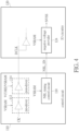
- FIG. 4 is a diagram illustrating the supply voltage configuration of the control circuit 110 and the IO circuitry 120 according to one embodiment of the present invention.
- the control circuit 110 comprises a pre-driver 112, a post-driver 114 and the timing control circuit 118, wherein the pre-driver 112 receives a signal to generate a processed signal, and the post-driver 114 receives the processed signal to generate a global IO signal to the IO circuitry 120.
- the pre-driver 112 is implemented by using an inverter, and the post-driver 114 is also implemented by an inverter, the clock signal CK' serves as the signal inputted into the pre-driver 112, and an output clock signal DCLK serves as the global IO signal.
- the pre-driver 112 may comprise more than one inverters connected in series, and the post-driver 114 may comprise more than one inverters connected in series.
- the pre-driver 112 is supplied by the supply voltage VSR_AM with higher voltage level, and the post-driver 114 is supplied by the supply voltage VCORE with lower voltage level. Because the pre-driver 112 is supplied by the supply voltage VSR_AM, an output signal of the pre-driver 112 will have higher voltage level, so that the post-driver 114 can generate the output clock signal DCLK with faster speed.
- the output signal of the inverter within the pre-driver 112 will have a high voltage level; and because the output signal of the inverter has the high voltage level such as VSRAM, an N-type transistor within the inverter of the post-driver 114 will be enabled with higher current, so that the post-driver 114 can generate the output clock signal DCLK having the low voltage level (e.g., 0V or ground voltage) in a short time.
- the control circuit 110 generates the output clock signal DCLK with faster speed, a hold time will be shortened when the input latch 128 uses the output clock signal DCLK to sample the input signal Din.
- the output clock signal DCLK is inputted into the IO circuitry 120, for use of the multiple components such as the input latch 128, the output driver 129, or the sense amplifier 126. That is, the IO circuitry 120 may have multiple paths, such as the inverters shown in FIG. 2 , for receiving the output clock signal DCLK.
- the pre-driver 112 receives the clock signal CK' that is generated by level-shifting the clock signal CK.
- the pre-driver 112 can receive the clock signal CK having lower voltage level.
- the pre-driver 112 and the post-driver 114 are supplied by using different supply voltages, however, the present invention is not limited to this. In another embodiment, the pre-driver 112 and the post-driver 114 can be supplied by the same supply voltage VSRAM, or all the components within the control circuit 110 are supplied by the supply voltage VSRAM. These alternative designs shall fall within the scope of the present invention.
- the negative voltage provider 124 within the IO circuitry 120 is supplied by the supply voltage VSRAM to stabilize the negative voltage level, and the other components such as the write driver 122, the input latch 123, the sense amplifier 126 and/or the output driver 127 is/are supplied by the supply voltage VCORE to lower the power consumption, so the memory device 100 can always have the stable write ability while maintaining low power consumption.
- the memory device of the present invention by designing the NBL timing control circuit and the negative voltage provider to be supplied by the supply voltage VSRAM that has a fixed voltage level, the memory device can always have stable write ability regardless whether the memory device operates in the normal mode or a power saving mode.
- the other components within the IO circuitry to use the supply voltage VCORE with lower voltage level, the memory device 100 can have the stable write ability while maintaining low power consumption.
- the present invention may also be defined by the following numbered clauses.
Landscapes
- Engineering & Computer Science (AREA)
- Microelectronics & Electronic Packaging (AREA)
- Computer Hardware Design (AREA)
- Power Engineering (AREA)
- Dram (AREA)
- Static Random-Access Memory (AREA)
Abstract
The present invention provides a memory device including a memory array, an IO circuitry and a control circuit. The IO circuitry includes a write buffer and a negative voltage provider. The write driver is configured to receive input data to drive bit lines of the memory array, and the negative voltage provider is configured to generate to generate a negative voltage to the write driver. The control circuit includes an NBL timing control circuit configured to generate an NBL enable signal to selectively enable the negative voltage provider. In addition, the memory device is supplied by a first supply voltage and a second supply voltage, a voltage level of the second supply voltage is higher than a voltage level of the first supply voltage, and the negative voltage provider and the NBL timing control circuit are supplied by the second supply voltage.
Description
- This application claims the benefit of
U.S. Provisional Application No. 63/490,308, filed on March 15th, 2023 - A dual-rail static random access memory (SRAM) has been widely used in various chips. The dual-rail SRAM refers to an SRAM arrangement where the logic circuits are operated in a low voltage domain, while the memory array is operated in a high voltage domain. Due to this, the chip area and the power consumption can be reduced but the memory access time or memory access speed is impacted, especially the memory access time will be greatly affected if the SRAM uses an ultra-low supply voltage.
- In addition, in order to improve the write ability, the SR_AM is generally designed to apply a negative voltage to a bit line of the memory array. However, since a voltage level of the negative voltage will be influenced by the supply voltage of the SR_AM, when the memory switches between two different supply voltages (e.g., the ultra-low supply voltage and a normal voltage) due to switching of operating modes, the negative voltage level will be unstable, causing writing problems to SRAM or increase the complexity of SR_AM design.
- It is therefore an objective of the present invention to provide a dual-rail memory device, which can reduce the impact of operating mode switching on the negative voltage level, to solve the above-mentioned problems.
- According to one embodiment of the present invention, a memory device comprising a memory array, an IO circuitry and a control circuit is disclosed. The IO circuitry is configured to access the memory array, and the IO circuitry comprises a write buffer and a negative voltage provider. The write driver is configured to receive input data to drive bit lines of the memory array, and the negative voltage provider is configured to generate to generate a negative voltage to the write driver. The control circuit comprises a negative-bit-line (NBL) timing control circuit configured to generate an NBL enable signal to selectively enable the negative voltage provider. In addition, the memory device is supplied by a first supply voltage and a second supply voltage, a voltage level of the second supply voltage is higher than a voltage level of the first supply voltage, and the negative voltage provider and the NBL timing control circuit are supplied by the second supply voltage.
- These and other objectives of the present invention will no doubt become obvious to those of ordinary skill in the art after reading the following detailed description of the preferred embodiment that is illustrated in the various figures and drawings.
-
-
FIG. 1 is a memory device according to one embodiment of the present invention. -
FIG. 2 is a diagram illustrating parts of circuit designs and the supply voltage configuration of the control circuit and the IO circuitry according to one embodiment of the present invention. -
FIG. 3 shows a timing diagram of parts of the signals of the memory device according to one embodiment of the present invention. -
FIG. 4 is a diagram illustrating the supply voltage configuration of the control circuit and the IO circuitry according to one embodiment of the present invention. - Certain terms are used throughout the following description and claims to refer to particular system components. As one skilled in the art will appreciate, manufacturers may refer to a component by different names. This document does not intend to distinguish between components that differ in name but not function. In the following discussion and in the claims, the terms "including" and "comprising" are used in an open-ended fashion, and thus should be interpreted to mean "including, but not limited to ...". The terms "couple" and "couples" are intended to mean either an indirect or a direct electrical connection. Thus, if a first device couples to a second device, that connection may be through a direct electrical connection, or through an indirect electrical connection via other devices and connections.
-
FIG. 1 is amemory device 100 according to one embodiment of the present invention. As shown inFIG. 1 , thememory device 100 comprises acontrol circuit 110, a input/output (IO)circuitry 120, asignal generator 130, a word-line driver 140 and amemory array 150, wherein theIO circuitry 120 comprises at least a write column multiplexer (mux) 121, awrite driver 122, aninput latch 123, anegative voltage provider 124, a read column multiplexer 125, asense amplifier 126 and anoutput driver 127. In this embodiment, thememory device 100 is a dual-rail SRAM circuitry, that is thememory device 100 uses supply voltages such as VCORE and VSRAM belonging to different power domains. In addition, thememory array 150 comprises a plurality of memory cells such as 6-transistor (6-T) SRAM cells, 8-T SRAM cells or 10-T SRAM cells. - In this embodiment, the
memory device 100 can operate in a power saving mode and a normal mode, wherein the supply voltage VCORE has different voltage levels for different modes, but the supply voltage VSR_AM is always the same. Specifically, when thememory device 100 operates in the normal mode, the supply voltage VCORE has a normal voltage level such as 0.7V, and the supply voltage VSRAM has a fixed voltage level higher than 0.7V; and when thememory device 100 operates in the power saving mode, the supply voltage VCORE has a ultra-low voltage level such as 0.5V, and the supply voltage VSRAM still have the fixed voltage level. - In addition, the
memory device 100 may comprise one or more level shift circuits such as 102 and 104 configured to increase voltage levels of the received signals. In one embodiment, without limitations of the present invention, thelevel shift circuit 102 is configured to receive the supply voltage VCORE to generate the supply voltage VSR_AM, and thelevel shift circuit 104 is configured to receive a clock signal CK to generate a clock signal CK' , wherein the voltage level of the supply voltage VSRAM is higher than the voltage level of the supply voltage VCORE, and the voltage level of the clock signal CK' is higher than the voltage level of the clock signal CK. In other embodiments, the supply voltage VSRAM with higher voltage level may be generated by another supply voltage generator, and the clock signal CK' with higher voltage level may be generated by another clock signal generator. - In the operation of the
memory device 100, thesignal generator 130 is configured to generate multiple signals for use of thecontrol circuit 110, for example, the multiple signals may comprise an address signal ADDR, a chip select signal CS, a write enable signal WE and the clock signal CK. Thecontrol circuit 110 may comprise a read/write timing control circuit, an address latch, a column decoder, a row decoder and other circuits, and thecontrol circuit 110 is configured to generate control signals and IO signals to the word-line driver 140 and theIO circuitry 120, respectively. The word-line driver 140 is configured to enable the word line of thememory array 150 based on the control signals generated by thecontrol circuit 110. Regarding theIO circuitry 120, theinput latch 123 is configured to receive input data Din from an external circuit. Thewrite driver 122 is configured to receive the input data Din from theinput latch 123 to write the input data into thememory array 150 via thewrite column multiplexer 121. Thenegative voltage provider 124 is configured to provide a negative voltage NVSS to thewrite driver 122 to improve the write ability. Thesense amplifier 126 is configured to read data from thememory array 150 via the read column multiplexer 125. Theoutput driver 127 is configured to generate output data Dout to the external circuit according to the data read by thesense amplifier 126. It is noted that the basic operations of the components within thememory device 100 are known by a person skilled in the art, and the present invention focuses on the supply voltage configurations of thememory device 100, so the detailed descriptions about the operations of the above components are omitted here. - In this embodiment, the word-
line driver 140 and thememory array 150 are supplied by the supply voltage VSR_AM with higher voltage level, so that thememory array 150 has a fast access speed. Thesignal generator 130 is supplied by the supply voltage VCORE with lower voltage level, so that thesignal generator 130 has lower power consumption and smaller chip area. Thecontrol circuit 110 is supplied by both the supply voltage VCORE and the supply voltage VSRAM, that is thecontrol circuit 110 has a first portion supplied by the supply voltage VCORE and a second portion supplied by the supply voltage VSRAM, so that thecontrol circuit 110 can maintain the signal transmission speed while reducing power consumption. In addition, theIO circuitry 120 is supplied by both the supply voltage VCORE and the supply voltage VSR_AM, that is theIO circuitry 120 has a first portion supplied by the supply voltage VCORE and a second portion supplied by the supply voltage VSR_AM, so that theIO circuitry 120 has the stable write ability while reducing power consumption. -
FIG. 2 is a diagram illustrating parts of circuit designs and the supply voltage configuration of thecontrol circuit 110 and theIO circuitry 120 according to one embodiment of the present invention. As shown inFIG. 2 , thecontrol circuit 110 comprises a negative-bit-line (NBL)timing control circuit 118, wherein the NBLtiming control circuit 118 is configured to generate an NBL enable signal NBL_EN to selectively enable thenegative voltage provider 124 to generate the negative voltage NVSS to thewrite driver 122. Thenegative voltage provider 124 comprises twoinverters inverters write driver 122. Thewrite driver 122 comprises twodrivers write column multiplexer 121 comprises two transistors M3 and M4 serving as two switches, wherein thedrivers input latch 123 to drive the bit-lines BL and BLB via the transistors M3 and M4, respectively. It is noted thatFIG. 2 only shows part of circuits of thewrite column multiplexer 121, thewrite driver 122 and thenegative voltage provider 124, and because the operations of circuit designs of thewrite column multiplexer 121, thewrite driver 122 and thenegative voltage provider 124 are known by a person skilled in the art, other examples are not provided here. - In the embodiment shown in
FIG. 2 , the NBLtiming control circuit 118 within thecontrol circuit 110 is supplied by the supply voltage VSRAM, and thenegative voltage provider 124 within theIO circuitry 120 is also supplied by the supply voltage VSRAM, so the bit line BL/BLB will have stable negative voltage regardless of whether thememory device 100 is operating in the normal mode or the power saving mode (i.e., regardless of whether the supply voltage VCORE has normal voltage level or ultra-low voltage level) . Therefore, thememory device 100 can have stable write ability at ultra-low voltage without additional circuit designs. -
FIG. 3 shows a timing diagram of parts of the signals of thememory device 100 according to one embodiment of the present invention. When thememory device 100 starts to write data into thememory array 150, the clock signal CK, the chip select signal CS and the write enable signal WE is enabled so that the word line (WL) is enabled. Then, the NBLtiming control circuit 118 generates the NBL enable signal NBL_EN to enable thenegative voltage provider 124 to generate the negative voltage NVSS to thewrite driver 122, to make the bit line BL or BLB has the negative voltage. In addition, regardless of whether the supply voltage VCORE has normal voltage level or ultra-low voltage level, the bit line BL/BLB will always have similar negative voltage level. -
FIG. 4 is a diagram illustrating the supply voltage configuration of thecontrol circuit 110 and theIO circuitry 120 according to one embodiment of the present invention. As shown inFIG. 4 , thecontrol circuit 110 comprises a pre-driver 112, a post-driver 114 and thetiming control circuit 118, wherein the pre-driver 112 receives a signal to generate a processed signal, and thepost-driver 114 receives the processed signal to generate a global IO signal to theIO circuitry 120. In this embodiment, without limitations of the present invention, the pre-driver 112 is implemented by using an inverter, and thepost-driver 114 is also implemented by an inverter, the clock signal CK' serves as the signal inputted into the pre-driver 112, and an output clock signal DCLK serves as the global IO signal. In other embodiments, the pre-driver 112 may comprise more than one inverters connected in series, and the post-driver 114 may comprise more than one inverters connected in series. - In the embodiment shown in
FIG. 4 , the pre-driver 112 is supplied by the supply voltage VSR_AM with higher voltage level, and the post-driver 114 is supplied by the supply voltage VCORE with lower voltage level. Because the pre-driver 112 is supplied by the supply voltage VSR_AM, an output signal of the pre-driver 112 will have higher voltage level, so that the post-driver 114 can generate the output clock signal DCLK with faster speed. Specifically, when the clock signal CK' has a low voltage level, the output signal of the inverter within the pre-driver 112 will have a high voltage level; and because the output signal of the inverter has the high voltage level such as VSRAM, an N-type transistor within the inverter of the post-driver 114 will be enabled with higher current, so that the post-driver 114 can generate the output clock signal DCLK having the low voltage level (e.g., 0V or ground voltage) in a short time. In addition, because thecontrol circuit 110 generates the output clock signal DCLK with faster speed, a hold time will be shortened when the input latch 128 uses the output clock signal DCLK to sample the input signal Din. - In addition, the output clock signal DCLK is inputted into the
IO circuitry 120, for use of the multiple components such as the input latch 128, the output driver 129, or thesense amplifier 126. That is, theIO circuitry 120 may have multiple paths, such as the inverters shown inFIG. 2 , for receiving the output clock signal DCLK. - In the embodiment shown in
FIG. 4 , the pre-driver 112 receives the clock signal CK' that is generated by level-shifting the clock signal CK. However, in other embodiments, the pre-driver 112 can receive the clock signal CK having lower voltage level. - In the above embodiment shown in
FIG. 4 , the pre-driver 112 and the post-driver 114 are supplied by using different supply voltages, however, the present invention is not limited to this. In another embodiment, the pre-driver 112 and the post-driver 114 can be supplied by the same supply voltage VSRAM, or all the components within thecontrol circuit 110 are supplied by the supply voltage VSRAM. These alternative designs shall fall within the scope of the present invention. - In one embodiment, the
negative voltage provider 124 within theIO circuitry 120 is supplied by the supply voltage VSRAM to stabilize the negative voltage level, and the other components such as thewrite driver 122, theinput latch 123, thesense amplifier 126 and/or theoutput driver 127 is/are supplied by the supply voltage VCORE to lower the power consumption, so thememory device 100 can always have the stable write ability while maintaining low power consumption. - Briefly summarized, in the memory device of the present invention, by designing the NBL timing control circuit and the negative voltage provider to be supplied by the supply voltage VSRAM that has a fixed voltage level, the memory device can always have stable write ability regardless whether the memory device operates in the normal mode or a power saving mode. In addition, by designing the other components within the IO circuitry to use the supply voltage VCORE with lower voltage level, the
memory device 100 can have the stable write ability while maintaining low power consumption. - Those skilled in the art will readily observe that numerous modifications and alterations of the device and method may be made while retaining the teachings of the invention. Accordingly, the above disclosure should be construed as limited only by the metes and bounds of the appended claims.
- The present invention may also be defined by the following numbered clauses.
- 1. A memory device, comprising:
- a memory array;
- an input/output (IO) circuitry, configured to access the memory array, wherein the IO circuit comprises:
- a write driver, configured to receive input data to drive bit lines of the memory array; and
- a negative voltage provider, configured to generate to generate a negative voltage to the write driver; and
- a control circuit, comprising:
a negative-bit-line (NBL) timing control circuit, configured to generate an NBL enable signal to selectively enable the negative voltage provider; - wherein the memory device is supplied by a first supply voltage and a second supply voltage, and a voltage level of the second supply voltage is higher than a voltage level of the first supply voltage; and the negative voltage provider and the NBL timing control circuit are supplied by the second supply voltage.
- 2. The memory device of clause 1, wherein when the memory array operates in a normal mode, the first supply voltage has a normal voltage level; and when the memory operates in a power saving mode, the first supply voltage has a low voltage level different from the normal voltage level; and the second supply voltage has the same voltage level regardless whether the memory device operates in the normal mode or the power saving mode.
- 3. The memory device of clause 1, wherein the IO circuitry further comprises a sense amplifier, an input latch and an output driver, and at least one of the write driver, the sense amplifier, the input larch and the output driver is supplied by the first supply voltage.
- 4. The memory device of clause 1, wherein the control circuit is supplied by both the first supply voltage and the second supply voltage.
- 5. The memory device of clause 4, wherein the control circuit comprises a pre-driver and a post-driver, the pre-driver is supplied by the second supply voltage, and the post-driver is supplied by the first supply voltage.
- 6. The memory device of clause 5, wherein the pre-driver receives a clock signal to generate a processed signal, and the post-driver receives the processed signal to generate an output clock signal serving as the global IO signal to the IO circuitry.
- 7. The memory device of clause 5, further comprising:
- a signal generator supplied by the first supply voltage, configured to generate a first clock signal; and
- a level shift circuit, configured to receive the first clock signal to generate the clock signal, wherein a voltage level of the clock signal is higher than a voltage level of the first clock signal.
- 8. The memory device of clause 5, wherein each of the pre-driver and the post-driver comprises an inverter.
- 9. The memory device of clause 1, wherein the memory device is a dual-rail static random access memory (SRAM) circuitry.
Claims (9)
- A memory device (100), comprising:a memory array (150);an input/output, IO, circuitry (120), configured to access the memory array (150), wherein the IO circuit comprises:a write driver (122), configured to receive input data to drive bit lines of the memory array (150); anda negative voltage provider (124), configured to generate to generate a negative voltage to the write driver (122); anda control circuit (110), comprising:
a negative-bit-line, NBL, timing control circuit (110), configured to generate an NBL enable signal to selectively enable the negative voltage provider (124);wherein the memory device (100) is supplied by a first supply voltage and a second supply voltage, and a voltage level of the second supply voltage is higher than a voltage level of the first supply voltage; and the negative voltage provider (124) and the NBL timing control circuit (118) are supplied by the second supply voltage. - The memory device (100) of claim 1, wherein when the memory array (150) operates in a normal mode, the first supply voltage has a normal voltage level; and when the memory operates in a power saving mode, the first supply voltage has a low voltage level different from the normal voltage level; and the second supply voltage has the same voltage level regardless whether the memory device (100) operates in the normal mode or the power saving mode.
- The memory device (100) of claim 1 or claim 2, wherein the IO circuitry (120) further comprises a sense amplifier (126), an input latch (123, 128) and an output driver (127, 129), and at least one of the write driver (122), the sense amplifier (126), the input larch and the output driver (127, 129) is supplied by the first supply voltage.
- The memory device (100) of claim 1, wherein the control circuit (110) is supplied by both the first supply voltage and the second supply voltage.
- The memory device (100) of claim 4, wherein the control circuit (110) comprises a pre-driver (112) and a post-driver (114), the pre-driver (112) is supplied by the second supply voltage, and the post-driver (114) is supplied by the first supply voltage.
- The memory device (100) of claim 5, wherein the pre-driver (112) receives a clock signal to generate a processed signal, and the post-driver (114) receives the processed signal to generate an output clock signal serving as the global IO signal to the IO circuitry (120).
- The memory device (100) of claim 5 or claim 6, further comprising:a signal generator (130) supplied by the first supply voltage, configured to generate a first clock signal; anda level shift circuit (102, 104), configured to receive the first clock signal to generate the clock signal, wherein a voltage level of the clock signal is higher than a voltage level of the first clock signal.
- The memory device (100) of any one of claims 5 to 7, wherein each of the pre-driver (112) and the post-driver (114) comprises an inverter.
- The memory device (100) according to any one of the preceding claims, wherein the memory device (100) is a dual-rail static random access memory, SRAM, circuitry.
Applications Claiming Priority (2)
| Application Number | Priority Date | Filing Date | Title |
|---|---|---|---|
| US202363490308P | 2023-03-15 | 2023-03-15 | |
| US18/444,754 US20240312514A1 (en) | 2023-03-15 | 2024-02-18 | Negative bit line control mechanism |
Publications (1)
| Publication Number | Publication Date |
|---|---|
| EP4432280A1 true EP4432280A1 (en) | 2024-09-18 |
Family
ID=90365714
Family Applications (1)
| Application Number | Title | Priority Date | Filing Date |
|---|---|---|---|
| EP24163622.4A Withdrawn EP4432280A1 (en) | 2023-03-15 | 2024-03-14 | Negative bit line control mechanism |
Country Status (2)
| Country | Link |
|---|---|
| US (1) | US20240312514A1 (en) |
| EP (1) | EP4432280A1 (en) |
Citations (2)
| Publication number | Priority date | Publication date | Assignee | Title |
|---|---|---|---|---|
| US20150146479A1 (en) * | 2013-11-22 | 2015-05-28 | International Business Machines Corporation | Sram write-assisted operation with vdd-to-vcs level shifting |
| US20190036513A1 (en) * | 2017-07-28 | 2019-01-31 | Taiwan Semiconductor Manufacturing Company, Ltd. | Clock generating circuit and method of operating the same |
-
2024
- 2024-02-18 US US18/444,754 patent/US20240312514A1/en active Pending
- 2024-03-14 EP EP24163622.4A patent/EP4432280A1/en not_active Withdrawn
Patent Citations (2)
| Publication number | Priority date | Publication date | Assignee | Title |
|---|---|---|---|---|
| US20150146479A1 (en) * | 2013-11-22 | 2015-05-28 | International Business Machines Corporation | Sram write-assisted operation with vdd-to-vcs level shifting |
| US20190036513A1 (en) * | 2017-07-28 | 2019-01-31 | Taiwan Semiconductor Manufacturing Company, Ltd. | Clock generating circuit and method of operating the same |
Also Published As
| Publication number | Publication date |
|---|---|
| US20240312514A1 (en) | 2024-09-19 |
| TW202439312A (en) | 2024-10-01 |
Similar Documents
| Publication | Publication Date | Title |
|---|---|---|
| US6903962B2 (en) | Semiconductor memory device capable of controlling potential level of power supply line and/or ground line | |
| US7643357B2 (en) | System and method for integrating dynamic leakage reduction with write-assisted SRAM architecture | |
| US6188628B1 (en) | Semiconductor storage device | |
| US8164971B2 (en) | Dual power rail word line driver and dual power rail word line driver array | |
| EP4432281A1 (en) | Dual-rail memory device with high speed and low power consumption | |
| US7466604B2 (en) | SRAM voltage control for improved operational margins | |
| US7085175B2 (en) | Word line driver circuit for a static random access memory and method therefor | |
| EP2329498B1 (en) | Dual power scheme in memory circuit | |
| US8164938B2 (en) | Semiconductor memory device | |
| US8259486B2 (en) | Self-timed write boost for SRAM cell with self mode control | |
| JP5621704B2 (en) | Semiconductor memory device | |
| US7259986B2 (en) | Circuits and methods for providing low voltage, high performance register files | |
| US5357479A (en) | Static random access memory capable of preventing erroneous writing | |
| US20030169076A1 (en) | Input buffer circuit and semiconductor memory device | |
| US6378008B1 (en) | Output data path scheme in a memory device | |
| JP2005085454A (en) | Integrated circuit device including a memory array and method for power gating in an integrated circuit device incorporating a memory having a sense amplifier | |
| US7034572B2 (en) | Voltage level shifting circuit and method | |
| US7242626B2 (en) | Method and apparatus for low voltage write in a static random access memory | |
| JP2008282515A (en) | Semiconductor memory device and method of testing the same | |
| US20240312514A1 (en) | Negative bit line control mechanism | |
| TWI917897B (en) | Memory device | |
| CN118675580A (en) | Memory device | |
| JP2006269023A (en) | Semiconductor memory apparatus | |
| US20020095544A1 (en) | Semiconductor memory device having memory cell block activation control circuit and method for controlling activation of memory cell blocks thereof | |
| JP2008047180A (en) | Semiconductor memory device |
Legal Events
| Date | Code | Title | Description |
|---|---|---|---|
| PUAI | Public reference made under article 153(3) epc to a published international application that has entered the european phase |
Free format text: ORIGINAL CODE: 0009012 |
|
| STAA | Information on the status of an ep patent application or granted ep patent |
Free format text: STATUS: THE APPLICATION HAS BEEN PUBLISHED |
|
| AK | Designated contracting states |
Kind code of ref document: A1 Designated state(s): AL AT BE BG CH CY CZ DE DK EE ES FI FR GB GR HR HU IE IS IT LI LT LU LV MC ME MK MT NL NO PL PT RO RS SE SI SK SM TR |
|
| STAA | Information on the status of an ep patent application or granted ep patent |
Free format text: STATUS: THE APPLICATION IS DEEMED TO BE WITHDRAWN |
|
| 18D | Application deemed to be withdrawn |
Effective date: 20250319 |