EP4430751B1 - Ein mehrstufiger pipeline-phasenrotator und seine anwendung in einer takt- und datenwiederherstellungsschleife - Google Patents
Ein mehrstufiger pipeline-phasenrotator und seine anwendung in einer takt- und datenwiederherstellungsschleife Download PDFInfo
- Publication number
- EP4430751B1 EP4430751B1 EP23829263.5A EP23829263A EP4430751B1 EP 4430751 B1 EP4430751 B1 EP 4430751B1 EP 23829263 A EP23829263 A EP 23829263A EP 4430751 B1 EP4430751 B1 EP 4430751B1
- Authority
- EP
- European Patent Office
- Prior art keywords
- stage
- phase
- rotators
- rotator
- bits
- Prior art date
- Legal status (The legal status is an assumption and is not a legal conclusion. Google has not performed a legal analysis and makes no representation as to the accuracy of the status listed.)
- Active
Links
Images












Classifications
-
- H—ELECTRICITY
- H03—ELECTRONIC CIRCUITRY
- H03L—AUTOMATIC CONTROL, STARTING, SYNCHRONISATION OR STABILISATION OF GENERATORS OF ELECTRONIC OSCILLATIONS OR PULSES
- H03L7/00—Automatic control of frequency or phase; Synchronisation
- H03L7/06—Automatic control of frequency or phase; Synchronisation using a reference signal applied to a frequency- or phase-locked loop
- H03L7/08—Details of the phase-locked loop
- H03L7/081—Details of the phase-locked loop provided with an additional controlled phase shifter
- H03L7/0812—Details of the phase-locked loop provided with an additional controlled phase shifter and where no voltage or current controlled oscillator is used
-
- H—ELECTRICITY
- H03—ELECTRONIC CIRCUITRY
- H03L—AUTOMATIC CONTROL, STARTING, SYNCHRONISATION OR STABILISATION OF GENERATORS OF ELECTRONIC OSCILLATIONS OR PULSES
- H03L7/00—Automatic control of frequency or phase; Synchronisation
- H03L7/06—Automatic control of frequency or phase; Synchronisation using a reference signal applied to a frequency- or phase-locked loop
- H03L7/08—Details of the phase-locked loop
- H03L7/099—Details of the phase-locked loop concerning mainly the controlled oscillator of the loop
- H03L7/0995—Details of the phase-locked loop concerning mainly the controlled oscillator of the loop the oscillator comprising a ring oscillator
- H03L7/0998—Details of the phase-locked loop concerning mainly the controlled oscillator of the loop the oscillator comprising a ring oscillator using phase interpolation
-
- H—ELECTRICITY
- H03—ELECTRONIC CIRCUITRY
- H03L—AUTOMATIC CONTROL, STARTING, SYNCHRONISATION OR STABILISATION OF GENERATORS OF ELECTRONIC OSCILLATIONS OR PULSES
- H03L7/00—Automatic control of frequency or phase; Synchronisation
- H03L7/06—Automatic control of frequency or phase; Synchronisation using a reference signal applied to a frequency- or phase-locked loop
- H03L7/08—Details of the phase-locked loop
- H03L7/0807—Details of the phase-locked loop concerning mainly a recovery circuit for the reference signal
-
- H—ELECTRICITY
- H03—ELECTRONIC CIRCUITRY
- H03L—AUTOMATIC CONTROL, STARTING, SYNCHRONISATION OR STABILISATION OF GENERATORS OF ELECTRONIC OSCILLATIONS OR PULSES
- H03L7/00—Automatic control of frequency or phase; Synchronisation
- H03L7/06—Automatic control of frequency or phase; Synchronisation using a reference signal applied to a frequency- or phase-locked loop
- H03L7/08—Details of the phase-locked loop
- H03L7/081—Details of the phase-locked loop provided with an additional controlled phase shifter
- H03L7/0812—Details of the phase-locked loop provided with an additional controlled phase shifter and where no voltage or current controlled oscillator is used
- H03L7/0814—Details of the phase-locked loop provided with an additional controlled phase shifter and where no voltage or current controlled oscillator is used the phase shifting device being digitally controlled
-
- H—ELECTRICITY
- H04—ELECTRIC COMMUNICATION TECHNIQUE
- H04L—TRANSMISSION OF DIGITAL INFORMATION, e.g. TELEGRAPHIC COMMUNICATION
- H04L7/00—Arrangements for synchronising receiver with transmitter
- H04L7/0016—Arrangements for synchronising receiver with transmitter correction of synchronization errors
- H04L7/002—Arrangements for synchronising receiver with transmitter correction of synchronization errors correction by interpolation
- H04L7/0025—Arrangements for synchronising receiver with transmitter correction of synchronization errors correction by interpolation interpolation of clock signal
-
- H—ELECTRICITY
- H03—ELECTRONIC CIRCUITRY
- H03K—PULSE TECHNIQUE
- H03K5/00—Manipulating of pulses not covered by one of the other main groups of this subclass
- H03K2005/00013—Delay, i.e. output pulse is delayed after input pulse and pulse length of output pulse is dependent on pulse length of input pulse
- H03K2005/00019—Variable delay
- H03K2005/00026—Variable delay controlled by an analog electrical signal, e.g. obtained after conversion by a D/A converter
- H03K2005/00052—Variable delay controlled by an analog electrical signal, e.g. obtained after conversion by a D/A converter by mixing the outputs of fixed delayed signals with each other or with the input signal
-
- H—ELECTRICITY
- H03—ELECTRONIC CIRCUITRY
- H03L—AUTOMATIC CONTROL, STARTING, SYNCHRONISATION OR STABILISATION OF GENERATORS OF ELECTRONIC OSCILLATIONS OR PULSES
- H03L7/00—Automatic control of frequency or phase; Synchronisation
- H03L7/06—Automatic control of frequency or phase; Synchronisation using a reference signal applied to a frequency- or phase-locked loop
- H03L7/08—Details of the phase-locked loop
- H03L7/085—Details of the phase-locked loop concerning mainly the frequency- or phase-detection arrangement including the filtering or amplification of its output signal
- H03L7/091—Details of the phase-locked loop concerning mainly the frequency- or phase-detection arrangement including the filtering or amplification of its output signal the phase or frequency detector using a sampling device
Definitions
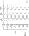
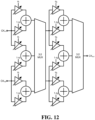
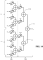
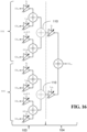
- Techniques herein include a method of pipelining PRs that results in power and area savings.
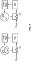
- a combination of pipelining and twin PRs creates a low power, jitter and area CDR loop.
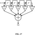
- the use of an FIR filter in a CDR loop helps to suppress phase noise and reduce jitter.
- the combination of these features enables the use of PRs in 200-Gb/s CDRs where strict jitter requirements have resulted in LC Voltage Controlled Oscillators (LCVCOs) being the only proven option.
- LCVCOs LC Voltage Controlled Oscillators
- a two-stage pipelined PR implemented with the method disclosed herein and with equal bits in stage one and stage two has a power and area reduction factor of (3)(2 - N /2 ). This power and area reduction factor is further improved if more bits are used in stage two or if additional stages are added to the PR.
- the jitter specifications of this PR will enable a low power and area CDR, and in turn a 200-Gb/s+ wireline transceiver that meets the ⁇ 75fs RMS random jitter standard.
- a SerDes ( Fig. 1 ) consists of two main blocks: a Transmitter (Tx) and a Receiver (Rx).
- Tx Transmitter
- Rx Receiver
- the Tx's main responsibility is to serialize many low-speed data paths into one high-speed data path.
- the Rx deserializes the high-speed data path into many low-speed data paths.
- SerDes become increasingly reliant on high-speed medium-resolution DACs and ADCs to perform their serialization and deserialization.
- High-speed DACs and ADCs can be further split into two parts: the data path and the clock path.
- the subject disclosure addresses the clock path which consumes a large portion of the DAC and ADC power budget.
- a DAC The basic purpose of a DAC is to receive an N-bit binary bus and convert it to a single analog signal. Modern DACs also perform serialization via cascaded multiplexers (MUXs) which use progressively higher-speed clocks as their select bit to combine several low-speed data paths.
- MUXs cascaded multiplexers
- Modern DACs and ADCs see Fig. 3 and Fig. 4 , have sampling rates in the range of 100-to-200 Gigasamples Per Second (GS/s) and could require multi-phase clocks operating anywhere from F s Rank 1 ⁇ Rank 2 to F s 2 .
- GS/s Gigasamples Per Second
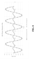
- INL is a measure of the output phase deviation from the ideal output phase.
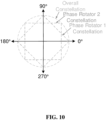
- Another method of improving PR linearity is to have CK in1 and CK in2 separated by 45°.
- Fig. 11 compares the theoretical INL for a traditional 6b quadrature PR to that of a twin 6b quadrature PR.
- FIR filters for example a Kaiser-Bessel FIR
- a Kaiser-Bessel FIR can be used to improve the stop band attenuation and 3-dB bandwidth without increasing the number of taps.
- the coefficients are calculated using a zeroth order modified Bessel function of the first kind.
- the stop band attenuation is around 40-dB and the 3-dB bandwidth is around 1GHz.
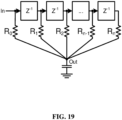
- An example of an analog FIR filter implementation can be seen in Fig. 19 . Summation is done in the voltage domain and the resistor values are modified to set the tap coefficients.
Landscapes
- Engineering & Computer Science (AREA)
- Computer Networks & Wireless Communication (AREA)
- Signal Processing (AREA)
- Stabilization Of Oscillater, Synchronisation, Frequency Synthesizers (AREA)
- Synchronisation In Digital Transmission Systems (AREA)
- Manipulation Of Pulses (AREA)
Claims (15)
- Mehrstufiger Pipeline-Phasenrotator, umfassend:eine erste Stufe (101, 103, 105), die eine erste Anzahl paralleler Phasenrotatoren umfasst, die jeweilige um einen festen Betrag versetzte Taktphasen erzeugen;eine zweite Stufe (102, 104, 106), die eine zweite Anzahl von Phasenrotatoren umfasst, die Ausgaben von der ersten Anzahl von Phasenrotatoren der ersten Stufe empfangen, wobei die zweite Stufe eine erste gewichtete Summe jeweiliger Taktphasen ausgibt, die von der zweiten Anzahl von Phasenrotatoren erzeugt werden;wobei die zweite Anzahl von Phasenrotatoren kleiner ist als die erste Anzahl von Phasenrotatoren undwobei eine Gesamtzahl der der Phasenauswahl gewidmeten Bits auf die erste und die zweite Stufe aufgeteilt ist.
- Mehrstufiger Pipeline-Phasenrotator nach Anspruch 1, wobei die erste Stufe eine erste Anzahl von Bits basierend auf der Gesamtzahl der der Phasenauswahl gewidmeten Bits aufweist, wobei die zweite Stufe eine zweite Anzahl von Bits basierend auf der Gesamtzahl der der Phasenauswahl gewidmeten Bits aufweist, wobei jeder Phasenrotator in der ersten Stufe eine erste Anzahl von Phaseninterpolator-Einheitszellen umfasst, die gemäß der ersten Anzahl von der Phasenauswahl gewidmeten Bits bestimmt wird, und wobei jeder Phasenrotator in der zweiten Stufe eine zweite Anzahl von Phaseninterpolator-Einheitszellen umfasst, die gemäß der zweiten Anzahl von der Phasenauswahl gewidmeten Bits bestimmt wird.
- Mehrstufiger Pipeline-Phasenrotator nach Anspruch 2, wobei die erste Stufe und die zweite Stufe weiter jeweils eine erste Vielzahl von Summierungsknoten (110) und eine zweite Vielzahl von Summierungsknoten (110) umfassen, die die Ausgaben von Phaseninterpolator-Einheitszellen jeweiliger Phasenrotatoren empfangen.
- Mehrstufiger Pipeline-Phasenrotator nach Anspruch 1, der weiter eine dritte Stufe (107) umfasst, die eine dritte Anzahl von Phasenrotatoren umfasst, die die Ausgaben von der zweiten Anzahl von Phasenrotatoren der zweiten Stufe empfangen, wobei die dritte Stufe eine zweite gewichtete Summe jeweiliger Taktphasen ausgibt, die von der dritten Anzahl von Phasenrotatoren erzeugt werden, wobei die dritte Anzahl von Phasenrotatoren kleiner als die zweite Anzahl von Phasenrotatoren ist.
- Mehrstufiger Pipeline-Phasenrotator nach Anspruch 2, wobei die zweite Anzahl von Bits, die der in der zweiten Stufe verwendeten Phasenauswahl gewidmet sind, größer ist als die erste Anzahl von Bits, die der in der ersten Stufe verwendeten Phasenauswahl gewidmet sind.
- Mehrstufiger Pipeline-Phasenrotator nach Anspruch 2, wobei die erste Anzahl von Phaseninterpolator-Einheitszellen und die zweite Anzahl von Phaseninterpolator-Einheitszellen Inverter mit steuerbarer variabler Antriebsstärke oder gemeinsamen Quellenverstärkern umfassen.
- Mehrstufiger Pipeline-Phasenrotator nach Anspruch 3, der weiter eine Zwischenstufe zwischen der ersten Stufe und der zweiten Stufe umfasst, wobei die Zwischenstufe eine dritte Vielzahl von Summierungsknoten umfasst, die die Ausgaben der ersten Vielzahl von Summierungsknoten empfängt.
- Mehrstufiger Pipeline-Phasenrotator nach Anspruch 1, wobei die Gesamtzahl der der Phasenauswahl in der ersten und der zweiten Stufe gewidmeten Bits neun beträgt.
- Verfahren, umfassend:paralleles Erzeugen jeweiliger Taktphasen, die um einen festen Betrag versetzt sind, wobei das Erzeugen durch eine erste Stufe (101, 103, 105) eines mehrstufigen Pipeline-Phasenrotators erfolgt, der eine erste Anzahl von Phasenrotatoren umfasst;Empfangen von Ausgaben von der ersten Anzahl von Phasenrotatoren der ersten Stufe durch eine zweite Stufe (102, 104, 106) des mehrstufigen Pipeline-Phasenrotators, der eine zweite Anzahl von Phasenrotatoren umfasst, wobei die zweite Stufe eine erste gewichtete Summe jeweiliger Taktphasen ausgibt, die von der zweiten Anzahl von Phasenrotatoren erzeugt werden;wobei die zweite Anzahl von Phasenrotatoren kleiner ist als die erste Anzahl von Phasenrotatoren undwobei eine Gesamtzahl der der Phasenauswahl gewidmeten Bits auf die erste und die zweite Stufe aufgeteilt ist.
- Verfahren nach Anspruch 9, wobei die erste Stufe eine erste Anzahl von Bits basierend auf der Gesamtzahl der der Phasenauswahl gewidmeten Bits aufweist, wobei die zweite Stufe eine zweite Anzahl von Bits basierend auf der Gesamtzahl der der Phasenauswahl gewidmeten Bits aufweist, wobei jeder Phasenrotator in der ersten Stufe eine erste Anzahl von Phaseninterpolator-Einheitszellen umfasst, die gemäß der ersten Anzahl von der Phasenauswahl gewidmeten Bits bestimmt wird, und wobei jeder Phasenrotator in der zweiten Stufe eine zweite Anzahl von Phaseninterpolator-Einheitszellen umfasst, die gemäß der zweiten Anzahl von der Phasenauswahl gewidmeten Bits bestimmt wird.
- Verfahren nach Anspruch 10, das das Empfangen der Ausgaben von Phaseninterpolator-Einheitszellen von jeweiligen Phasenrotatoren durch eine erste Vielzahl von Summierungsknoten (110) der ersten Stufe bzw. eine zweite Vielzahl von Summierungsknoten (110) der zweiten Stufe umfasst.
- Verfahren nach Anspruch 9, das weiter das Empfangen der Ausgaben von der zweiten Anzahl von Phasenrotatoren der zweiten Stufe durch eine dritte Stufe (107) des mehrstufigen Pipeline-Phasenrotators umfasst, der eine dritte Anzahl von Phasenrotatoren umfasst, wobei die dritte Stufe eine zweite gewichtete Summe jeweiliger Taktphasen ausgibt, die von der dritten Anzahl von Phasenrotatoren erzeugt werden, wobei die dritte Anzahl von Phasenrotatoren kleiner als die zweite Anzahl von Phasenrotatoren ist.
- Verfahren nach Anspruch 10, wobei die zweite Anzahl von Bits, die der in der zweiten Stufe verwendeten Phasenauswahl gewidmet ist, größer ist als die erste Anzahl von Bits, die der in der ersten Stufe verwendeten Phasenauswahl gewidmet ist.
- Verfahren nach Anspruch 10, wobei die erste Anzahl von Phaseninterpolator-Einheitszellen und die zweite Anzahl von Phaseninterpolator-Einheitszellen Inverter mit steuerbarer variabler Antriebsstärke oder gemeinsamen Quellenverstärkern umfassen.
- Verfahren nach Anspruch 11, wobei sich zwischen der ersten Stufe und der zweiten Stufe eine Zwischenstufe befindet, wobei die Zwischenstufe eine dritte Vielzahl von Summierungsknoten umfasst, die die Ausgaben der ersten Vielzahl von Summierungsknoten empfängt.
Applications Claiming Priority (2)
| Application Number | Priority Date | Filing Date | Title |
|---|---|---|---|
| US18/060,787 US12176908B2 (en) | 2022-12-01 | 2022-12-01 | Method and apparatus for clock and data alignment that reduces power consumption |
| PCT/US2023/081519 WO2024118714A2 (en) | 2022-12-01 | 2023-11-29 | Method and apparatus for clock and data alignment that reduces power consumption |
Publications (2)
| Publication Number | Publication Date |
|---|---|
| EP4430751A2 EP4430751A2 (de) | 2024-09-18 |
| EP4430751B1 true EP4430751B1 (de) | 2025-04-09 |
Family
ID=89385901
Family Applications (1)
| Application Number | Title | Priority Date | Filing Date |
|---|---|---|---|
| EP23829263.5A Active EP4430751B1 (de) | 2022-12-01 | 2023-11-29 | Ein mehrstufiger pipeline-phasenrotator und seine anwendung in einer takt- und datenwiederherstellungsschleife |
Country Status (4)
| Country | Link |
|---|---|
| US (2) | US12176908B2 (de) |
| EP (1) | EP4430751B1 (de) |
| CN (1) | CN120303879A (de) |
| WO (1) | WO2024118714A2 (de) |
Families Citing this family (2)
| Publication number | Priority date | Publication date | Assignee | Title |
|---|---|---|---|---|
| US12249990B1 (en) | 2023-11-15 | 2025-03-11 | Ciena Corporation | Apparatus and method for wideband multi-phase clock generation |
| US12489451B2 (en) | 2023-11-15 | 2025-12-02 | Ciena Corporation | Multiphase clock generator |
Family Cites Families (15)
| Publication number | Priority date | Publication date | Assignee | Title |
|---|---|---|---|---|
| US7050522B2 (en) * | 2000-05-26 | 2006-05-23 | International Business Machines Corporation | Phase rotator and data recovery receiver incorporating said phase rotator |
| US7653167B2 (en) * | 2006-09-07 | 2010-01-26 | Intel Corporation | Phase deglitch circuit for phase interpolator for high-speed serial I/O applications |
| US7864080B1 (en) * | 2008-12-29 | 2011-01-04 | Altera Corporation | Sample rate conversion by controlled selection of filter outputs |
| US8552783B2 (en) | 2011-06-10 | 2013-10-08 | International Business Machines Corporation | Programmable delay generator and cascaded interpolator |
| US8564352B2 (en) * | 2012-02-10 | 2013-10-22 | International Business Machines Corporation | High-resolution phase interpolators |
| US8912837B2 (en) | 2012-10-12 | 2014-12-16 | Stmicroelectronics S.R.L. | Mux-based digital delay interpolator |
| US9166605B2 (en) * | 2013-03-18 | 2015-10-20 | Terasquare Co., Ltd. | Low-power and all-digital phase interpolator-based clock and data recovery architecture |
| US9882709B2 (en) * | 2016-05-10 | 2018-01-30 | Macom Connectivity Solutions, Llc | Timing recovery with adaptive channel response estimation |
| US20180106889A1 (en) * | 2016-10-14 | 2018-04-19 | Lockheed Martin Corporation | System and method for radar based threat determination and classification |
| US10483956B2 (en) | 2017-07-20 | 2019-11-19 | Rohm Co., Ltd. | Phase interpolator, timing generator, and semiconductor integrated circuit |
| KR102403623B1 (ko) * | 2017-08-18 | 2022-05-30 | 삼성전자주식회사 | 클록 신호들 사이의 스큐를 조절하도록 구성되는 전자 회로 |
| US10484167B2 (en) * | 2018-03-13 | 2019-11-19 | Xilinx, Inc. | Circuit for and method of receiving a signal in an integrated circuit device |
| CN110417407B (zh) * | 2018-04-27 | 2022-11-22 | 瑞昱半导体股份有限公司 | 时钟数据恢复装置 |
| US11233519B1 (en) | 2021-05-10 | 2022-01-25 | Ciena Corporation | Phase skipping technique for high-speed, high-phase number delay locked loop |
| US11463093B1 (en) | 2021-05-12 | 2022-10-04 | Ciena Corporation | Reducing non-linearities of a phase rotator |
-
2022
- 2022-12-01 US US18/060,787 patent/US12176908B2/en active Active
-
2023
- 2023-11-29 CN CN202380082693.0A patent/CN120303879A/zh active Pending
- 2023-11-29 WO PCT/US2023/081519 patent/WO2024118714A2/en not_active Ceased
- 2023-11-29 EP EP23829263.5A patent/EP4430751B1/de active Active
-
2024
- 2024-11-12 US US18/944,162 patent/US20250070789A1/en active Pending
Also Published As
| Publication number | Publication date |
|---|---|
| WO2024118714A2 (en) | 2024-06-06 |
| US20250070789A1 (en) | 2025-02-27 |
| CN120303879A (zh) | 2025-07-11 |
| WO2024118714A3 (en) | 2024-07-04 |
| EP4430751A2 (de) | 2024-09-18 |
| US12176908B2 (en) | 2024-12-24 |
| US20240187008A1 (en) | 2024-06-06 |
Similar Documents
| Publication | Publication Date | Title |
|---|---|---|
| US20250070789A1 (en) | Method and apparatus for clock and data alignment that reduces power consumption | |
| US7532053B2 (en) | Phase interpolation apparatus, systems, and methods | |
| CN114153136B (zh) | 一种基于时钟校准技术的全周期数字时间转换器 | |
| US6552619B2 (en) | Multi-channel clock recovery circuit | |
| US8330632B2 (en) | Self-healing analog-to-digital converters with background calibration | |
| Greshishchev et al. | A 56GS/s 6b DAC in 65nm CMOS with 256× 6b memory | |
| Baert et al. | 20.1 a 5GS/s 7.2 ENOB time-interleaved VCO-based ADC achieving 30.5 fJ/conv-step | |
| WO2018089509A1 (en) | High linearity phase interpolator | |
| WO2008033979A2 (en) | Gated ring oscillator for a time-to-digital converter with shaped quantization noise | |
| US11641210B1 (en) | Matrix processor generating SAR-searched input delay adjustments to calibrate timing skews in a multi-channel interleaved analog-to-digital converter (ADC) | |
| EP3772182B1 (de) | Analog-digital-wandler auf basis eines spannungsgesteuerten oszillators mit einem maximallängen-sequenzgenerator | |
| CN111628775A (zh) | 基于多数表决的比较器失调校准装置和校准方法 | |
| EP4037192B1 (de) | Grob-/fein-zählarchitektur für vco-adc basierend auf verriegelten binären asynchronen zählern | |
| KR20080056240A (ko) | 지연 로크 루프 회로, 타이밍 발생기, 반도체 시험 장치,반도체 집적 회로 및 지연량 교정 방법 | |
| US6035409A (en) | 1000 mb phase picker clock recovery architecture using interleaved phase detectors | |
| CN119543934B (zh) | 基于空时平均与相位插值技术的小数多模分频器电路 | |
| EP4599522B1 (de) | Vorrichtung und verfahren zur breitbandigen mehrphasentakterzeugung | |
| CN113376999A (zh) | 一种用于高时间分辨率时间数字转换器的特殊加法器 | |
| KR20090043636A (ko) | 전압제어발진기 기반의 아날로그 디지털 변환기, 아날로그디지털 변환방법 및 전압제어발진기 기반의 엔차 아날로그디지털 변환기 | |
| Yao et al. | A high-resolution time-to-digital converter based on parallel delay elements | |
| US12489451B2 (en) | Multiphase clock generator | |
| Shah et al. | An 8b 5-GS/s CMOS SAR ADC with speed optimized SAR logic | |
| Cui et al. | High speed data converters and their applications in optical communication system | |
| Guo et al. | A broadband mismatch calibration prototype application-specific integrated circuit for time-interleaved analog-to-digital converter systems | |
| Kong et al. | A Multiplexed Low Power and High Linearity Cascaded Phase Interpolator Design |
Legal Events
| Date | Code | Title | Description |
|---|---|---|---|
| STAA | Information on the status of an ep patent application or granted ep patent |
Free format text: STATUS: UNKNOWN |
|
| STAA | Information on the status of an ep patent application or granted ep patent |
Free format text: STATUS: THE INTERNATIONAL PUBLICATION HAS BEEN MADE |
|
| PUAI | Public reference made under article 153(3) epc to a published international application that has entered the european phase |
Free format text: ORIGINAL CODE: 0009012 |
|
| STAA | Information on the status of an ep patent application or granted ep patent |
Free format text: STATUS: REQUEST FOR EXAMINATION WAS MADE |
|
| 17P | Request for examination filed |
Effective date: 20240611 |
|
| AK | Designated contracting states |
Kind code of ref document: A2 Designated state(s): AL AT BE BG CH CY CZ DE DK EE ES FI FR GB GR HR HU IE IS IT LI LT LU LV MC ME MK MT NL NO PL PT RO RS SE SI SK SM TR |
|
| GRAP | Despatch of communication of intention to grant a patent |
Free format text: ORIGINAL CODE: EPIDOSNIGR1 |
|
| STAA | Information on the status of an ep patent application or granted ep patent |
Free format text: STATUS: GRANT OF PATENT IS INTENDED |
|
| INTG | Intention to grant announced |
Effective date: 20241017 |
|
| P01 | Opt-out of the competence of the unified patent court (upc) registered |
Free format text: CASE NUMBER: APP_61415/2024 Effective date: 20241115 |
|
| GRAS | Grant fee paid |
Free format text: ORIGINAL CODE: EPIDOSNIGR3 |
|
| GRAA | (expected) grant |
Free format text: ORIGINAL CODE: 0009210 |
|
| STAA | Information on the status of an ep patent application or granted ep patent |
Free format text: STATUS: THE PATENT HAS BEEN GRANTED |
|
| AK | Designated contracting states |
Kind code of ref document: B1 Designated state(s): AL AT BE BG CH CY CZ DE DK EE ES FI FR GB GR HR HU IE IS IT LI LT LU LV MC ME MK MT NL NO PL PT RO RS SE SI SK SM TR |
|
| DAV | Request for validation of the european patent (deleted) | ||
| DAX | Request for extension of the european patent (deleted) | ||
| REG | Reference to a national code |
Ref country code: GB Ref legal event code: FG4D |
|
| REG | Reference to a national code |
Ref country code: CH Ref legal event code: EP |
|
| REG | Reference to a national code |
Ref country code: DE Ref legal event code: R096 Ref document number: 602023002862 Country of ref document: DE |
|
| REG | Reference to a national code |
Ref country code: IE Ref legal event code: FG4D |
|
| REG | Reference to a national code |
Ref country code: NL Ref legal event code: FP |
|
| REG | Reference to a national code |
Ref country code: AT Ref legal event code: MK05 Ref document number: 1784480 Country of ref document: AT Kind code of ref document: T Effective date: 20250409 |
|
| PG25 | Lapsed in a contracting state [announced via postgrant information from national office to epo] |
Ref country code: FI Free format text: LAPSE BECAUSE OF FAILURE TO SUBMIT A TRANSLATION OF THE DESCRIPTION OR TO PAY THE FEE WITHIN THE PRESCRIBED TIME-LIMIT Effective date: 20250409 Ref country code: ES Free format text: LAPSE BECAUSE OF FAILURE TO SUBMIT A TRANSLATION OF THE DESCRIPTION OR TO PAY THE FEE WITHIN THE PRESCRIBED TIME-LIMIT Effective date: 20250409 Ref country code: PT Free format text: LAPSE BECAUSE OF FAILURE TO SUBMIT A TRANSLATION OF THE DESCRIPTION OR TO PAY THE FEE WITHIN THE PRESCRIBED TIME-LIMIT Effective date: 20250811 |
|
| REG | Reference to a national code |
Ref country code: LT Ref legal event code: MG9D |
|
| PG25 | Lapsed in a contracting state [announced via postgrant information from national office to epo] |
Ref country code: NO Free format text: LAPSE BECAUSE OF FAILURE TO SUBMIT A TRANSLATION OF THE DESCRIPTION OR TO PAY THE FEE WITHIN THE PRESCRIBED TIME-LIMIT Effective date: 20250709 Ref country code: GR Free format text: LAPSE BECAUSE OF FAILURE TO SUBMIT A TRANSLATION OF THE DESCRIPTION OR TO PAY THE FEE WITHIN THE PRESCRIBED TIME-LIMIT Effective date: 20250710 |
|
| PG25 | Lapsed in a contracting state [announced via postgrant information from national office to epo] |
Ref country code: PL Free format text: LAPSE BECAUSE OF FAILURE TO SUBMIT A TRANSLATION OF THE DESCRIPTION OR TO PAY THE FEE WITHIN THE PRESCRIBED TIME-LIMIT Effective date: 20250409 |
|
| PG25 | Lapsed in a contracting state [announced via postgrant information from national office to epo] |
Ref country code: BG Free format text: LAPSE BECAUSE OF FAILURE TO SUBMIT A TRANSLATION OF THE DESCRIPTION OR TO PAY THE FEE WITHIN THE PRESCRIBED TIME-LIMIT Effective date: 20250409 |
|
| PG25 | Lapsed in a contracting state [announced via postgrant information from national office to epo] |
Ref country code: HR Free format text: LAPSE BECAUSE OF FAILURE TO SUBMIT A TRANSLATION OF THE DESCRIPTION OR TO PAY THE FEE WITHIN THE PRESCRIBED TIME-LIMIT Effective date: 20250409 |
|
| PG25 | Lapsed in a contracting state [announced via postgrant information from national office to epo] |
Ref country code: AT Free format text: LAPSE BECAUSE OF FAILURE TO SUBMIT A TRANSLATION OF THE DESCRIPTION OR TO PAY THE FEE WITHIN THE PRESCRIBED TIME-LIMIT Effective date: 20250409 |
|
| PG25 | Lapsed in a contracting state [announced via postgrant information from national office to epo] |
Ref country code: RS Free format text: LAPSE BECAUSE OF FAILURE TO SUBMIT A TRANSLATION OF THE DESCRIPTION OR TO PAY THE FEE WITHIN THE PRESCRIBED TIME-LIMIT Effective date: 20250709 |
|
| PG25 | Lapsed in a contracting state [announced via postgrant information from national office to epo] |
Ref country code: IS Free format text: LAPSE BECAUSE OF FAILURE TO SUBMIT A TRANSLATION OF THE DESCRIPTION OR TO PAY THE FEE WITHIN THE PRESCRIBED TIME-LIMIT Effective date: 20250809 |
|
| PG25 | Lapsed in a contracting state [announced via postgrant information from national office to epo] |
Ref country code: LV Free format text: LAPSE BECAUSE OF FAILURE TO SUBMIT A TRANSLATION OF THE DESCRIPTION OR TO PAY THE FEE WITHIN THE PRESCRIBED TIME-LIMIT Effective date: 20250409 |
|
| PGFP | Annual fee paid to national office [announced via postgrant information from national office to epo] |
Ref country code: DE Payment date: 20251119 Year of fee payment: 3 |
|
| REG | Reference to a national code |
Ref country code: DE Ref legal event code: R097 Ref document number: 602023002862 Country of ref document: DE |
|
| PG25 | Lapsed in a contracting state [announced via postgrant information from national office to epo] |
Ref country code: DK Free format text: LAPSE BECAUSE OF FAILURE TO SUBMIT A TRANSLATION OF THE DESCRIPTION OR TO PAY THE FEE WITHIN THE PRESCRIBED TIME-LIMIT Effective date: 20250409 Ref country code: SM Free format text: LAPSE BECAUSE OF FAILURE TO SUBMIT A TRANSLATION OF THE DESCRIPTION OR TO PAY THE FEE WITHIN THE PRESCRIBED TIME-LIMIT Effective date: 20250409 |
|
| PGFP | Annual fee paid to national office [announced via postgrant information from national office to epo] |
Ref country code: FR Payment date: 20251126 Year of fee payment: 3 |
|
| PG25 | Lapsed in a contracting state [announced via postgrant information from national office to epo] |
Ref country code: CZ Free format text: LAPSE BECAUSE OF FAILURE TO SUBMIT A TRANSLATION OF THE DESCRIPTION OR TO PAY THE FEE WITHIN THE PRESCRIBED TIME-LIMIT Effective date: 20250409 |
|
| PG25 | Lapsed in a contracting state [announced via postgrant information from national office to epo] |
Ref country code: EE Free format text: LAPSE BECAUSE OF FAILURE TO SUBMIT A TRANSLATION OF THE DESCRIPTION OR TO PAY THE FEE WITHIN THE PRESCRIBED TIME-LIMIT Effective date: 20250409 |
|
| PG25 | Lapsed in a contracting state [announced via postgrant information from national office to epo] |
Ref country code: SK Free format text: LAPSE BECAUSE OF FAILURE TO SUBMIT A TRANSLATION OF THE DESCRIPTION OR TO PAY THE FEE WITHIN THE PRESCRIBED TIME-LIMIT Effective date: 20250409 |
|
| PG25 | Lapsed in a contracting state [announced via postgrant information from national office to epo] |
Ref country code: IT Free format text: LAPSE BECAUSE OF FAILURE TO SUBMIT A TRANSLATION OF THE DESCRIPTION OR TO PAY THE FEE WITHIN THE PRESCRIBED TIME-LIMIT Effective date: 20250409 |
|
| PLBE | No opposition filed within time limit |
Free format text: ORIGINAL CODE: 0009261 |
|
| STAA | Information on the status of an ep patent application or granted ep patent |
Free format text: STATUS: NO OPPOSITION FILED WITHIN TIME LIMIT |
|
| REG | Reference to a national code |
Ref country code: CH Ref legal event code: L10 Free format text: ST27 STATUS EVENT CODE: U-0-0-L10-L00 (AS PROVIDED BY THE NATIONAL OFFICE) Effective date: 20260218 |
|
| PG25 | Lapsed in a contracting state [announced via postgrant information from national office to epo] |
Ref country code: RO Free format text: LAPSE BECAUSE OF FAILURE TO SUBMIT A TRANSLATION OF THE DESCRIPTION OR TO PAY THE FEE WITHIN THE PRESCRIBED TIME-LIMIT Effective date: 20250409 |
|
| 26N | No opposition filed |
Effective date: 20260112 |