EP4429412A1 - Circuit-forming method and circuit-forming apparatus - Google Patents
Circuit-forming method and circuit-forming apparatus Download PDFInfo
- Publication number
- EP4429412A1 EP4429412A1 EP21963204.9A EP21963204A EP4429412A1 EP 4429412 A1 EP4429412 A1 EP 4429412A1 EP 21963204 A EP21963204 A EP 21963204A EP 4429412 A1 EP4429412 A1 EP 4429412A1
- Authority
- EP
- European Patent Office
- Prior art keywords
- resin
- mark
- forming
- curable resin
- wiring
- Prior art date
- Legal status (The legal status is an assumption and is not a legal conclusion. Google has not performed a legal analysis and makes no representation as to the accuracy of the status listed.)
- Pending
Links
Images





Classifications
-
- H—ELECTRICITY
- H05—ELECTRIC TECHNIQUES NOT OTHERWISE PROVIDED FOR
- H05K—PRINTED CIRCUITS; CASINGS OR CONSTRUCTIONAL DETAILS OF ELECTRIC APPARATUS; MANUFACTURE OF ASSEMBLAGES OF ELECTRICAL COMPONENTS
- H05K3/00—Apparatus or processes for manufacturing printed circuits
- H05K3/10—Apparatus or processes for manufacturing printed circuits in which conductive material is applied to the insulating support in such a manner as to form the desired conductive pattern
- H05K3/12—Apparatus or processes for manufacturing printed circuits in which conductive material is applied to the insulating support in such a manner as to form the desired conductive pattern using thick film techniques, e.g. printing techniques to apply the conductive material or similar techniques for applying conductive paste or ink patterns
- H05K3/1241—Apparatus or processes for manufacturing printed circuits in which conductive material is applied to the insulating support in such a manner as to form the desired conductive pattern using thick film techniques, e.g. printing techniques to apply the conductive material or similar techniques for applying conductive paste or ink patterns by ink-jet printing or drawing by dispensing
- H05K3/125—Apparatus or processes for manufacturing printed circuits in which conductive material is applied to the insulating support in such a manner as to form the desired conductive pattern using thick film techniques, e.g. printing techniques to apply the conductive material or similar techniques for applying conductive paste or ink patterns by ink-jet printing or drawing by dispensing by ink-jet printing
-
- H—ELECTRICITY
- H05—ELECTRIC TECHNIQUES NOT OTHERWISE PROVIDED FOR
- H05K—PRINTED CIRCUITS; CASINGS OR CONSTRUCTIONAL DETAILS OF ELECTRIC APPARATUS; MANUFACTURE OF ASSEMBLAGES OF ELECTRICAL COMPONENTS
- H05K3/00—Apparatus or processes for manufacturing printed circuits
- H05K3/46—Manufacturing multilayer circuits
- H05K3/4644—Manufacturing multilayer circuits by building the multilayer layer by layer, i.e. build-up multilayer circuits
- H05K3/4664—Adding a circuit layer by thick film methods, e.g. printing techniques or by other techniques for making conductive patterns by using pastes, inks or powders
-
- B—PERFORMING OPERATIONS; TRANSPORTING
- B33—ADDITIVE MANUFACTURING TECHNOLOGY
- B33Y—ADDITIVE MANUFACTURING, i.e. MANUFACTURING OF THREE-DIMENSIONAL [3D] OBJECTS BY ADDITIVE DEPOSITION, ADDITIVE AGGLOMERATION OR ADDITIVE LAYERING, e.g. BY 3D PRINTING, STEREOLITHOGRAPHY OR SELECTIVE LASER SINTERING
- B33Y10/00—Processes of additive manufacturing
-
- H—ELECTRICITY
- H05—ELECTRIC TECHNIQUES NOT OTHERWISE PROVIDED FOR
- H05K—PRINTED CIRCUITS; CASINGS OR CONSTRUCTIONAL DETAILS OF ELECTRIC APPARATUS; MANUFACTURE OF ASSEMBLAGES OF ELECTRICAL COMPONENTS
- H05K3/00—Apparatus or processes for manufacturing printed circuits
- H05K3/0085—Apparatus for treatments of printed circuits with liquids not provided for in groups H05K3/02 - H05K3/46; conveyors and holding means therefor
- H05K3/0088—Apparatus for treatments of printed circuits with liquids not provided for in groups H05K3/02 - H05K3/46; conveyors and holding means therefor for treatment of holes
-
- H—ELECTRICITY
- H05—ELECTRIC TECHNIQUES NOT OTHERWISE PROVIDED FOR
- H05K—PRINTED CIRCUITS; CASINGS OR CONSTRUCTIONAL DETAILS OF ELECTRIC APPARATUS; MANUFACTURE OF ASSEMBLAGES OF ELECTRICAL COMPONENTS
- H05K3/00—Apparatus or processes for manufacturing printed circuits
- H05K3/10—Apparatus or processes for manufacturing printed circuits in which conductive material is applied to the insulating support in such a manner as to form the desired conductive pattern
- H05K3/12—Apparatus or processes for manufacturing printed circuits in which conductive material is applied to the insulating support in such a manner as to form the desired conductive pattern using thick film techniques, e.g. printing techniques to apply the conductive material or similar techniques for applying conductive paste or ink patterns
- H05K3/1258—Apparatus or processes for manufacturing printed circuits in which conductive material is applied to the insulating support in such a manner as to form the desired conductive pattern using thick film techniques, e.g. printing techniques to apply the conductive material or similar techniques for applying conductive paste or ink patterns by using a substrate provided with a shape pattern, e.g. grooves, banks, resist pattern
-
- H—ELECTRICITY
- H05—ELECTRIC TECHNIQUES NOT OTHERWISE PROVIDED FOR
- H05K—PRINTED CIRCUITS; CASINGS OR CONSTRUCTIONAL DETAILS OF ELECTRIC APPARATUS; MANUFACTURE OF ASSEMBLAGES OF ELECTRICAL COMPONENTS
- H05K3/00—Apparatus or processes for manufacturing printed circuits
- H05K3/30—Assembling printed circuits with electric components, e.g. with resistors
- H05K3/303—Assembling printed circuits with electric components, e.g. with resistors with surface mounted components
-
- H—ELECTRICITY
- H05—ELECTRIC TECHNIQUES NOT OTHERWISE PROVIDED FOR
- H05K—PRINTED CIRCUITS; CASINGS OR CONSTRUCTIONAL DETAILS OF ELECTRIC APPARATUS; MANUFACTURE OF ASSEMBLAGES OF ELECTRICAL COMPONENTS
- H05K1/00—Printed circuits
- H05K1/02—Details
- H05K1/0266—Marks, test patterns or identification means
- H05K1/0269—Marks, test patterns or identification means for visual or optical inspection
-
- H—ELECTRICITY
- H05—ELECTRIC TECHNIQUES NOT OTHERWISE PROVIDED FOR
- H05K—PRINTED CIRCUITS; CASINGS OR CONSTRUCTIONAL DETAILS OF ELECTRIC APPARATUS; MANUFACTURE OF ASSEMBLAGES OF ELECTRICAL COMPONENTS
- H05K2201/00—Indexing scheme relating to printed circuits covered by H05K1/00
- H05K2201/09—Shape and layout
- H05K2201/09818—Shape or layout details not covered by a single group of H05K2201/09009 - H05K2201/09809
- H05K2201/09918—Optically detected marks used for aligning tool relative to the PCB, e.g. for mounting of components
-
- H—ELECTRICITY
- H05—ELECTRIC TECHNIQUES NOT OTHERWISE PROVIDED FOR
- H05K—PRINTED CIRCUITS; CASINGS OR CONSTRUCTIONAL DETAILS OF ELECTRIC APPARATUS; MANUFACTURE OF ASSEMBLAGES OF ELECTRICAL COMPONENTS
- H05K2203/00—Indexing scheme relating to apparatus or processes for manufacturing printed circuits covered by H05K3/00
- H05K2203/01—Tools for processing; Objects used during processing
- H05K2203/0104—Tools for processing; Objects used during processing for patterning or coating
- H05K2203/0126—Dispenser, e.g. for solder paste, for supplying conductive paste for screen printing or for filling holes
-
- H—ELECTRICITY
- H05—ELECTRIC TECHNIQUES NOT OTHERWISE PROVIDED FOR
- H05K—PRINTED CIRCUITS; CASINGS OR CONSTRUCTIONAL DETAILS OF ELECTRIC APPARATUS; MANUFACTURE OF ASSEMBLAGES OF ELECTRICAL COMPONENTS
- H05K2203/00—Indexing scheme relating to apparatus or processes for manufacturing printed circuits covered by H05K3/00
- H05K2203/01—Tools for processing; Objects used during processing
- H05K2203/0104—Tools for processing; Objects used during processing for patterning or coating
- H05K2203/013—Inkjet printing, e.g. for printing insulating material or resist
-
- H—ELECTRICITY
- H05—ELECTRIC TECHNIQUES NOT OTHERWISE PROVIDED FOR
- H05K—PRINTED CIRCUITS; CASINGS OR CONSTRUCTIONAL DETAILS OF ELECTRIC APPARATUS; MANUFACTURE OF ASSEMBLAGES OF ELECTRICAL COMPONENTS
- H05K2203/00—Indexing scheme relating to apparatus or processes for manufacturing printed circuits covered by H05K3/00
- H05K2203/07—Treatments involving liquids, e.g. plating, rinsing
- H05K2203/0756—Uses of liquids, e.g. rinsing, coating, dissolving
- H05K2203/0763—Treating individual holes or single row of holes, e.g. by nozzle
-
- H—ELECTRICITY
- H05—ELECTRIC TECHNIQUES NOT OTHERWISE PROVIDED FOR
- H05K—PRINTED CIRCUITS; CASINGS OR CONSTRUCTIONAL DETAILS OF ELECTRIC APPARATUS; MANUFACTURE OF ASSEMBLAGES OF ELECTRICAL COMPONENTS
- H05K2203/00—Indexing scheme relating to apparatus or processes for manufacturing printed circuits covered by H05K3/00
- H05K2203/14—Related to the order of processing steps
- H05K2203/1438—Treating holes after another process, e.g. coating holes after coating the substrate
-
- H—ELECTRICITY
- H05—ELECTRIC TECHNIQUES NOT OTHERWISE PROVIDED FOR
- H05K—PRINTED CIRCUITS; CASINGS OR CONSTRUCTIONAL DETAILS OF ELECTRIC APPARATUS; MANUFACTURE OF ASSEMBLAGES OF ELECTRICAL COMPONENTS
- H05K3/00—Apparatus or processes for manufacturing printed circuits
- H05K3/0008—Apparatus or processes for manufacturing printed circuits for aligning or positioning of tools relative to the circuit board
-
- H—ELECTRICITY
- H05—ELECTRIC TECHNIQUES NOT OTHERWISE PROVIDED FOR
- H05K—PRINTED CIRCUITS; CASINGS OR CONSTRUCTIONAL DETAILS OF ELECTRIC APPARATUS; MANUFACTURE OF ASSEMBLAGES OF ELECTRICAL COMPONENTS
- H05K3/00—Apparatus or processes for manufacturing printed circuits
- H05K3/40—Forming printed elements for providing electric connections to or between printed circuits
- H05K3/4038—Through-connections; Vertical interconnect access [VIA] connections
- H05K3/4053—Through-connections; Vertical interconnect access [VIA] connections by thick-film techniques
- H05K3/4069—Through-connections; Vertical interconnect access [VIA] connections by thick-film techniques for via connections in organic insulating substrates
-
- H—ELECTRICITY
- H05—ELECTRIC TECHNIQUES NOT OTHERWISE PROVIDED FOR
- H05K—PRINTED CIRCUITS; CASINGS OR CONSTRUCTIONAL DETAILS OF ELECTRIC APPARATUS; MANUFACTURE OF ASSEMBLAGES OF ELECTRICAL COMPONENTS
- H05K3/00—Apparatus or processes for manufacturing printed circuits
- H05K3/46—Manufacturing multilayer circuits
- H05K3/4644—Manufacturing multilayer circuits by building the multilayer layer by layer, i.e. build-up multilayer circuits
- H05K3/4679—Aligning added circuit layers or via connections relative to previous circuit layers
Definitions
- the present invention relates to a circuit-forming method or the like in which a resin layer including a recessed portion is formed of a curable resin, and an electrode is formed inside the recessed portion by a conductive paste.
- Patent Literature 1 WO2020/250381
- An object of the present description is to appropriately form an electrode inside a recessed portion of a resin layer by a conductive paste.
- the present description discloses a circuit-forming method including a first forming step of forming a resin layer including a recessed portion by a first discharge device configured to discharge a curable resin, and a second forming step of forming an electrode inside the recessed portion by a second discharge device, which is configured to discharge a conductive paste, by referring to a first mark formed by the first discharge device.
- the present description discloses a circuit-forming apparatus including a first discharge device that forms a resin layer including a recessed portion by discharging a curable resin, and a second discharge device that forms an electrode inside the recessed portion by discharging a conductive paste by referring to a first mark formed by the first discharge device.
- a resin layer including a recessed portion is formed by a first discharge device configured to discharge a curable resin, and an electrode is formed inside the recessed portion by a second discharge device, which is configured to discharge a conductive paste, by referring to a first mark formed by the first discharge device.
- the electrode can be appropriately formed by the conductive paste inside the recessed portion of the resin layer.
- Fig. 1 illustrates circuit-forming apparatus 10 of a first embodiment.
- Circuit-forming apparatus 10 includes conveyance device 20, first shaping unit 22, second shaping unit 23, third shaping unit 24, mounting unit 26, imaging unit 27, and control device 28 (refer to Fig. 2 ).
- Conveyance device 20, first shaping unit 22, second shaping unit 23, third shaping unit 24, mounting unit 26, and imaging unit 27 are disposed on base 29 of circuit-forming apparatus 10.
- Base 29 has a generally rectangular shape, and in the following description, a longer direction of base 29 will be referred to as an X-axis direction, a shorter direction of base 29 will be referred to as a Y-axis direction, and a direction orthogonal to both the X-axis direction and the Y-axis direction will be referred to as a Z-axis direction.
- Conveyance device 20 is provided with X-axis slide mechanism 30 and Y-axis slide mechanism 32.
- X-axis slide mechanism 30 includes X-axis slide rail 34 and X-axis slider 36.
- X-axis slide rail 34 is disposed on base 29 to extend in the X-axis direction.
- X-axis slider 36 is held by X-axis slide rail 34 to be slidable in the X-axis direction.
- X-axis slide mechanism 30 further includes electromagnetic motor 38 (refer to Fig. 2 ), and X-axis slider 36 is moved to any position in the X-axis direction by driving electromagnetic motor 38.
- Y-axis slide mechanism 32 includes Y-axis slide rail 50 and stage 52.
- Y-axis slide rail 50 is disposed on base 29 to extend in the Y-axis direction and is movable in the X-axis direction. Then, one end portion of Y-axis slide rail 50 is coupled to X-axis slider 36. Stage 52 is held on Y-axis slide rail 50 to be slidable in the Y-axis direction. Furthermore, Y-axis slide mechanism 32 includes electromagnetic motor 56 (refer to Fig. 2 ), and stage 52 is moved to any position in the Y-axis direction by driving electromagnetic motor 56. As a result, stage 52 is moved to any position on base 29 with the driving of X-axis slide mechanism 30 and Y-axis slide mechanism 32.
- Stage 52 includes base plate 60, holding devices 62, and lifting and lowering device 64.
- Base plate 60 is formed in a flat plate shape, and a board is placed on an upper surface of base plate 60.
- Holding devices 62 are provided on both side portions of base plate 60 in the X-axis direction. Then, both edge portions of pallet 70 (refer to Fig. 3 ) placed on base plate 60 in the X-axis direction are sandwiched by holding devices 62, so that pallet 70 is fixedly held.
- lifting and lowering device 64 is disposed below base plate 60, and lifts and lowers base plate 60.
- First shaping unit 22 is a unit that shapes a wiring on pallet 70 placed on base plate 60 of stage 52, and includes first printing section 72 and sintering section 74.
- First printing section 72 includes inkjet head 76 (refer to Fig. 2 ), and inkjet head 76 linearly discharges metal ink.
- the metal ink is ink obtained by dispersing nanometer-sized metal fine particles, for example, silver fine particles in a solvent. A surface of the metal fine particles is coated with a dispersant and aggregation in the solvent is prevented.
- inkjet head 76 discharges the metal ink from multiple nozzles by, for example, a piezo method using a piezoelectric element.
- Sintering section 74 includes infrared irradiation device 78 (refer to Fig. 2 ).
- Infrared irradiation device 78 is a device for irradiating the discharged metal ink with infrared light, and the metal ink irradiated with infrared light is sintered to form the wiring.
- Sintering of the metal ink is, for example, a phenomenon in which evaporation of a solvent or decomposition of a protective film of metal fine particles, that is, a dispersant, or the like is performed by applying energy, so that conductivity is increased by contacting or fusing the metal fine particles. Then, the metal ink is sintered to form a metal wiring.
- second shaping unit 23 is a unit that shapes a resin layer on pallet 70 placed on base plate 60 of stage 52, and includes second printing section 84 and curing section 86.
- Second printing section 84 includes inkjet head 88 (refer to Fig. 2 ), and inkjet head 88 discharges an ultraviolet curable resin.
- the ultraviolet curable resin is a resin that is cured by irradiation with ultraviolet light.
- Inkjet head 88 may be, for example, a piezo type using a piezoelectric element, or may be a thermal type in which a resin is heated to generate air bubbles, which are discharged from multiple nozzles.
- Curing section 86 includes flattening device 90 (refer to Fig. 2 ) and irradiation device 92 (refer to Fig. 2 ).
- Flattening device 90 flattens an upper surface of the ultraviolet curable resin discharged by inkjet head 88, and makes the thickness of the ultraviolet curable resin uniform, for example, by scraping off excess resin by a roller or a blade while leveling the surface of the ultraviolet curable resin.
- irradiation device 92 includes a mercury lamp or LED as a light source, and irradiates the discharged ultraviolet curable resin with ultraviolet light. As a result, the discharged ultraviolet curable resin is cured to form the resin layer.
- Third shaping unit 24 is a unit that shapes a connection portion between an electrode of an electronic component and the wiring on pallet 70 placed on base plate 60 of stage 52, and includes third printing section 100 and first heating section 102.
- Third printing section 100 includes dispenser 106 (refer to Fig. 2 ), and dispenser 106 discharges conductive resin paste.
- the conductive resin paste is paste in which micrometer-sized metal particles are dispersed in a resin cured by heating at a relatively low temperature. Incidentally, the metal particles are flake-shaped, and viscosity of the conductive resin paste is relatively higher than that of the metal ink.
- the discharge amount of the conductive resin paste by dispenser 106 is controlled by an inner diameter of a needle, the pressure during discharge, and the discharge time.
- First heating section 102 includes heater 108 (refer to Fig. 2 ).
- Heater 108 is a device that heats the conductive resin paste applied by dispenser 106, and a resin is cured in the heated conductive resin paste.
- the resin in the conductive resin paste, the resin is cured and contracted, and the dispersed flake-shaped metal particles contact the resin.
- the conductive resin paste exhibits conductivity.
- the resin of the conductive resin paste is an organic adhesive, and exhibits an adhesive force when cured by heating.
- mounting unit 26 is a unit for mounting the electronic component on pallet 70 placed on base plate 60 of stage 52, and includes supply section 120 and mounting section 122.
- Supply section 120 includes multiple tape feeders 124 (refer to Fig. 2 ) that feed the taped electronic components one by one, and supplies the electronic component to the supply position.
- Supply section 120 is not limited to tape feeder 124, and may be a tray-type supply device that supplies the electronic component by picking up the electronic component from a tray.
- supply section 120 may include both of the tape-type supply device and the tray-type supply device, or other supply devices.
- Mounting section 122 includes mounting head 126 (refer to Fig. 2 ) and moving device 128 (refer to Fig. 2 ).
- Mounting head 126 includes a suction nozzle (not illustrated) for picking up and holding the electronic component.
- the suction nozzle picks up and holds the electronic component by suction of air as a negative pressure is supplied from a positive and negative pressure supply device (not illustrated). Then, as a slight positive pressure is supplied from the positive and negative pressure supply device, the electronic component is separated.
- moving device 128 moves mounting head 126 between the supply position of the electronic component by tape feeder 124 and pallet 70 placed on base plate 60. As a result, in mounting section 122, the electronic component supplied from tape feeder 124 is held by the suction nozzle, and the electronic component held by the suction nozzle is mounted on pallet 70.
- Imaging unit 27 is a unit for imaging pallet 70 placed on base plate 60 of stage 52, and includes camera 130.
- Camera 130 is disposed above base 29 in a posture facing downward, and images the upper surface of pallet 70 placed on base plate 60 of stage 52 from the above.
- control device 28 is provided with controller 150, multiple drive circuits 152, and image processing device 154.
- Multiple drive circuits 152 are connected to electromagnetic motors 38 and 56, holding device 62, lifting and lowering device 64, inkjet head 76, infrared irradiation device 78, inkjet head 88, flattening device 90, irradiation device 92, dispenser 106, heater 108, tape feeder 124, mounting head 126, and moving device 128.
- Controller 150 includes CPU, ROM, RAM, or the like, mainly includes a computer, and is connected to multiple drive circuits 152.
- controller 150 controls the operations of conveyance device 20, first shaping unit 22, second shaping unit 23, third shaping unit 24, and mounting unit 26.
- controller 150 is connected to image processing device 154.
- Image processing device 154 is for processing the imaging data obtained by camera 130, and controller 150 acquires various information from the imaging data.
- circuit-forming apparatus 10 With the configuration described above, in circuit-forming apparatus 10, a resin stack is formed on pallet 70, and a wiring is formed on the upper surface of the resin stack. Then, the electrodes of the electronic component are electrically connected to the wiring via the conductive resin paste.
- pallet 70 is set on base plate 60 of stage 52, and stage 52 is moved below second shaping unit 23. Then, in second shaping unit 23, as illustrated in Fig. 3 , resin stack 160 is formed on pallet 70. Resin stack 160 is formed by repeating the discharge of the ultraviolet curable resin from inkjet head 88 and the irradiation with ultraviolet light by irradiation device 92 to the discharged ultraviolet curable resin.
- inkjet head 88 discharges the ultraviolet curable resin in a thin film shape on the upper surface of pallet 70. Subsequently, when the ultraviolet curable resin is discharged in the thin film shape, the surface of the ultraviolet curable resin is flattened by flattening device 90 in curing section 86 such that the ultraviolet curable resin has a uniform film thickness. Then, irradiation device 92 irradiates the thin film-shaped ultraviolet curable resin with ultraviolet light. As a result, thin film-shaped resin layer 162 is formed on pallet 70.
- inkjet head 88 discharges the ultraviolet curable resin in a thin film shape onto thin film-shaped resin layer 162.
- the thin film-shaped ultraviolet curable resin is flattened by flattening device 90, irradiation device 92 irradiates the ultraviolet curable resin discharged in a thin film shape with ultraviolet light, and thus thin film-shaped resin layer 162 is stacked on thin film-shaped resin layer 162.
- the discharge of the ultraviolet curable resin onto thin film-shaped resin layer 162, the flattening of the surface of the ultraviolet curable resin, and the curing of the ultraviolet curable resin are repeated, and multiple resin layers 162 are stacked and thus resin stack 160 is formed.
- resin stack 160 is formed in a generally rectangular shape when viewed from above.
- generally block-shaped first base 166 is formed on pallet 70 adjacent to the four corners of rectangular resin stack 160.
- First base 166 is formed in the same manner as resin stack 160. That is, after the ultraviolet curable resin is discharged in a thin film shape and the surface of the ultraviolet curable resin is flattened by flattening device 90, the ultraviolet curable resin is cured by the irradiation of the ultraviolet curable resin with the ultraviolet light. As a result, a resin layer is formed. Then, the discharge of the ultraviolet curable resin, the flattening of the surface of the ultraviolet curable resin, and the curing of the ultraviolet curable resin are repeated and the resin layers are stacked, and thus first base 166 is formed.
- stage 52 is moved below first shaping unit 22.
- inkjet head 76 linearly discharges metal ink 168 on the upper surface of resin stack 160 in accordance with the circuit pattern.
- infrared irradiation device 78 irradiates metal ink 168 discharged in accordance with the circuit pattern with infrared light in sintering section 74 of first shaping unit 22.
- metal ink 168 is sintered, and wiring 170 is formed on resin stack 160.
- metal mark 172 is formed on first base 166. That is, in first printing section 72 of first shaping unit 22, inkjet head 76 discharges metal ink 174 in a circular shape onto first base 166. Subsequently, infrared irradiation device 78 irradiates metal ink 174 discharged in a circular shape with infrared light in sintering section 74 of first shaping unit 22. As a result, metal ink 174 is sintered, and metal mark 172 is formed on first base 166.
- resin stack 176 is formed on resin stack 160.
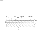
- resin stack 176 is formed by the same method as that of resin stack 160, resin stack 176 has hole 178, and the end portion of wiring 170 formed on resin stack 160 is exposed to hole 178. Therefore, when resin stack 176 is formed, the ultraviolet curable resin is discharged onto the upper surface of resin stack 160 such that the end portion of wiring 170 is exposed. After the surface of the ultraviolet curable resin is flattened by flattening device 90, the ultraviolet curable resin is cured by the irradiation of the ultraviolet curable resin with the ultraviolet light.
- stage 52 is moved below third shaping unit 24. Then, in third printing section 100 of third shaping unit 24, dispenser 106 discharges the conductive resin paste into hole 178 of resin stack 176. At this time, dispenser 106 refers to metal mark 172 and discharges the conductive resin paste onto the end portion of wiring 170.
- stage 52 is moved below imaging unit 27. Then, in imaging unit 27, camera 130 images four metal marks 172 formed on first base 166. Then, the imaging data obtained through the imaging is analyzed in controller 150, and the positions of four metal marks 172 are calculated based on the imaging data. As a result, the formation position of wiring 170 formed by inkjet head 76 in similar manner as metal mark 172 can be appropriately recognized.
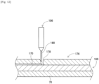
- Stage 52 is moved below third shaping unit 24, and the operation of conveyance device 20 is controlled based on the position of metal mark 172 such that dispenser 106 is positioned above the end portion of wiring 170 in third printing section 100 of third shaping unit 24. As a result, dispenser 106 and the end portion of wiring 170 are appropriately matched. Then, stage 52 is raised by the operation of lifting and lowering device 64, so that, as illustrated in Fig. 7 , the distal end of nozzle 180 of dispenser 106 enters the inside of hole 178 of resin stack 176. This is because the end portion of wiring 170 is exposed to hole 178. Then, when the distal end of nozzle 180 of dispenser 106 enters the inside of hole 178, dispenser 106 discharges the conductive resin paste.
- dispenser 106 discharges conductive resin paste 182 in an amount that fills the inside of hole 178.
- conductive resin paste 182 is heated by heater 108.
- conductive resin paste 182 is made conductive and functions as an electrode, so that conductive resin paste 182 and wiring 170 are electrically connected.
- Conductive resin paste 182 is referred to as connection electrode 184.
- stage 52 is moved below first shaping unit 22.
- inkjet head 76 linearly discharges metal ink 186 on the upper surface of resin stack 176 in accordance with the circuit pattern.
- inkjet head 76 discharges metal ink 186 onto the upper surface of resin stack 176 such that one end of metal ink 186 is in contact with connection electrode 184.
- infrared irradiation device 78 irradiates metal ink 186 with infrared light in sintering section 74 of first shaping unit 22.
- metal ink 186 is sintered, and wiring 188 electrically connected to wiring 170 via connection electrode 184 is formed on resin stack 176.
- stage 52 is moved below third shaping unit 24.
- dispenser 106 discharges conductive resin paste 190 onto the end portion of wiring 188, as illustrated in Fig. 10 .
- dispenser 106 refers to metal mark 172 and discharges conductive resin paste 190 onto the end portion of wiring 188. That is, the operation of conveyance device 20 is controlled based on the position of metal mark 172 such that dispenser 106 is positioned above the end portion of wiring 188. As a result, dispenser 106 and the end portion of wiring 188 are appropriately matched.
- dispenser 106 discharges conductive resin paste 190 onto the end portion of wiring 188.
- stage 52 is moved below mounting unit 26.
- electronic component 200 (refer to Fig. 11 ) is supplied by tape feeder 124, and electronic component 200 is held by the suction nozzle of mounting head 126.
- electronic component 200 is configured with component body 202 and two electrodes 204 disposed on the lower surface of component body 202.
- mounting head 126 is moved by moving device 128, and electronic component 200 held by suction nozzle is mounted on the upper surface of resin stack 176.
- electronic component 200 is mounted on the upper surface of resin stack 176 such that electrode 204 of electronic component 200 is in contact with conductive resin paste 190 discharged onto wiring 188.
- stage 52 is moved below third shaping unit 24. Then, in first heating section 102 of third shaping unit 24, conductive resin paste 190 is heated by heater 108. As a result, conductive resin paste 190 exhibits conductivity, so that electrode 204 is electrically connected to wiring 188 via conductive resin paste 190. In addition, electronic component 200 is fixed to resin stack 176 by being fixed to wiring 188 due to the adhesive force of conductive resin paste 190.
- wiring 170 formed on resin stack 160 and wiring 188 formed on resin stack 176 are electrically connected to each other via connection electrode 184 formed in hole 178 of resin stack 176.
- electrode 204 of electronic component 200 is electrically connected to wiring 188 via conductive resin paste 190, so that circuit 210 is formed.
- conductive resin paste 182 discharged when connection electrode 184 connecting wiring 170 and wiring 188 is formed and conductive resin paste 190 connecting wiring 188 and electrode 204 of electronic component 200 are discharged by referring to metal mark 172.
- conductive resin pastes 182 and 190 can be appropriately discharged onto wirings 170 and 188, and conduction in circuit 210 is ensured.
- nozzle 180 of dispenser 106 abuts the inner wall surface defining hole 178 of resin stack 176 as illustrated in Fig. 12 , and nozzle 180 may be damaged.
- nozzle 180 does not abut the inner wall surface defining hole 178, nozzle 180 does not appropriately enter the inside of hole 178, and there is a case in which conductive resin paste 182 cannot be discharged into hole 178. In such a case, discharge failure of conductive resin paste 182 may occur, and conduction failure in the circuit may occur.
- the ultraviolet curable resin which is the material of resin stack 176
- the metal ink which is the material of wiring 170
- the expansion coefficient due to heating is also different, and deviation occurs in the nozzle pitch between inkjet head 76 and inkjet head 88. Therefore, a relative positional deviation occurs between the formation position of wiring 170 and the formation position of hole 178 of resin stack 176.
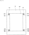
- dispenser 106 discharges the conductive resin paste by referring to the mark formed of the ultraviolet curable resin that is the material of resin stack 176. More specifically, in second shaping unit 23, when resin stack 160 and four first bases 166 are formed, as illustrated in Fig. 13 , four second bases 220 are also formed adjacent to four first bases 166. Second base 220 is formed in the same manner as first base 166. That is, after the ultraviolet curable resin is discharged in a thin film shape and the surface of the ultraviolet curable resin is flattened by flattening device 90, the ultraviolet curable resin is cured by the irradiation of the ultraviolet curable resin with the ultraviolet light.
- Resin mark 222 is formed on each second base 220 by using the ultraviolet curable resin.
- Resin mark 222 is formed by a method different from that of second base 220. More specifically, after the ultraviolet curable resin is discharged in a thin film shape and the surface of the ultraviolet curable resin is not flattened by flattening device 90, the ultraviolet curable resin is cured by the irradiation of the ultraviolet curable resin with the ultraviolet light. As a result, a resin layer is formed. Then, the discharge of the ultraviolet curable resin and the curing of the ultraviolet curable resin are repeated and the resin layers are stacked, and thus resin mark 222 is formed. Resin mark 222 is generally formed in a circular shape.
- stage 52 is moved below imaging unit 27.
- imaging unit 27 camera 130 images four resin marks 222 formed on four second bases 220.
- the imaging data obtained through the imaging is analyzed in controller 150, and the positions of four resin marks 222 are calculated based on the imaging data.
- the formation position of hole 178 of resin stack 176 formed by inkjet head 88 in similar manner as resin mark 222 can be appropriately recognized.
- resin mark 222 is formed of the same material as that of second base 220, that is, the ultraviolet curable resin
- resin mark 222 is formed by a method different from that of second base 220, so that the position of resin mark 222 can be calculated appropriately based on the imaging data of resin mark 222. More specifically, when the resin mark is formed by the same method as the second base, the resin mark is formed of the same material as the second base, so that the reflectance of the surface of the resin mark and the reflectance of the surface of the second base are substantially the same. As described above, when the reflectance of the surface of the resin mark and the reflectance of the surface of the second base are substantially the same, it is difficult to recognize the outer edge of the resin mark formed on the second base based on the imaging data.
- second base 220 when second base 220 is formed, as described above, the surface of the ultraviolet curable resin is flattened by flattening device 90 before the ultraviolet curable resin is irradiated with ultraviolet light. Therefore, although the surface of second base 220 is flat, there is very small unevenness in a microscopic manner. Meanwhile, when resin mark 222 is formed, the surface of the ultraviolet curable resin is not flattened by flattening device 90, and the ultraviolet curable resin is irradiated with ultraviolet light. Therefore, although the surface of resin mark 222 is not flat, there is almost no microscopic unevenness due to the surface tension or the like of the ultraviolet curable resin.
- the reflectance of the surface of resin mark 222 is different from the reflectance of the surface of second base 220, and the outer edge of resin mark 222 formed on second base 220 can be appropriately recognized based on the imaging data.
- the position of resin mark 222 can be appropriately calculated based on the imaging data of resin mark 222.
- dispenser 106 discharges the conductive paste onto wiring 170 via hole 178 of resin stack 176 based on the calculated position of resin mark 222. That is, when the conductive resin paste is discharged onto wiring 170 via hole 178, the operation of conveyance device 20 is controlled based on the position of resin mark 222 such that dispenser 106 is positioned above hole 178 in third printing section 100 of third shaping unit 24. As a result, nozzle 180 and hole 178 of dispenser 106 are appropriately matched in a vertical direction. Then, stage 52 is raised by the operation of lifting and lowering device 64, so that, as illustrated in Fig.
- dispenser 106 discharges the conductive resin paste, so that the conductive resin paste is discharged onto wiring 170 exposed inside hole 178.
- dispenser 106 refers to resin mark 222 and discharges the conductive resin paste, so that the conductive resin paste can be appropriately discharged onto wiring 170 via hole 178 of resin stack 176. As a result, it is possible to prevent abutment of nozzle 180 with the inner wall surface defining hole 178, the occurrence of discharge failure of the conductive resin paste, or the like.
- dispenser 106 discharges the conductive resin paste by referring to metal mark 172.
- the conductive resin paste can be appropriately discharged onto wiring 188, and the conduction between wiring 188 and electrode 204 of electronic component 200 can be secured.
- dispenser 106 discharges the conductive resin paste by referring to resin mark 222, and when the conductive resin paste is discharged onto wiring 188, dispenser 106 discharges the conductive resin paste referring to metal mark 172.
- abutment of nozzle 180 with the inner wall surface defining hole 178, the occurrence of discharge failure of the conductive resin paste, or the like can be prevented, and conduction between wiring 188 and electrode 204 of electronic component 200 can be secured.
- metal mark 172 is formed on first base 166, and resin mark 222 is formed on second base 220.
- metal mark 172 is formed on first base 166, and resin mark 222 is formed on metal mark 172.
- the outer diameter of resin mark 222 is smaller than the outer diameter of metal mark 172.
- resin mark 222 is formed on metal mark 172, so that the disposition space for metal mark 172 and resin mark 222 can be reduced.
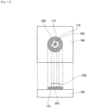
- metal mark 172 is formed on first base 166, and resin mark 250 having a circular ring shape is formed on metal mark 172.
- the outer diameter of resin mark 250 is smaller than the outer diameter of metal mark 172.
- controller 150 calculates the position of resin mark 250 by recognizing the boundary between the inner wall surface defining cavity 252 at the center of resin mark 250 and the outer edge of metal mark 172 exposed via cavity 252 based on the imaging data. As a result, the position of resin mark 250 can be appropriately calculated.
- controller 150 of control device 28 includes first forming section 260, second forming section 262, third forming section 264, fourth forming section 266, and discharge section 268.
- First forming section 260 is a functional section for forming resin stacks 160 and 176, first base 166, second base 220, and resin mark 222.
- Second forming section 262 is a functional section for forming connection electrode 184 inside hole 178 by referring to resin mark 222.
- Third forming section 264 is a functional section for forming wiring 188.
- Fourth forming section 266 is a functional section for forming resin mark 222 on metal mark 172.
- Discharge section 268 is a functional section for discharging the conductive resin paste onto wiring 188 by referring to metal mark 172.
- circuit-forming apparatus 10 is an example of a circuit-forming apparatus.
- Inkjet head 76 is an example of a third discharge device.
- Inkjet head 88 is an example of a first discharge device.
- Flattening device 90 is an example of a flattening device.
- Dispenser 106 is an example of a second discharge device.
- Metal mark 172 is an example of a second mark.
- Resin stack 176 is an example of a resin layer. Hole 178 is an example of a recessed portion.
- Connection electrode 184 is an example of an electrode.
- Wiring 188 is an example of a wiring.
- Second base 220 is an example of a base.
- Resin mark 222 is an example of a first mark.
- Resin mark 250 is an example of a first mark.
- a step performed by first forming section 260 is an example of a first forming step.
- a step performed by second forming section 262 is an example of a second forming step.
- a step performed by third forming section 264 is an example of a third forming step.
- a step by fourth forming section 266 is an example of a fourth forming step.
- a step performed by discharge section 268 is an example of a discharging step.
- resin mark 222 is formed on metal mark 172, but metal mark 172 may be formed on resin mark 222.
- annular-shaped resin mark 250 is formed on metal mark 172, but the annular-shaped metal mark may be formed on resin mark 222.
- the surface of the ultraviolet curable resin when second base 220 is formed, the surface of the ultraviolet curable resin is flattened before the ultraviolet curable resin is irradiated with ultraviolet light, and when resin mark 222 is formed, the ultraviolet curable resin is irradiated with ultraviolet light without flattening the surface of the ultraviolet curable resin. Meanwhile, when resin mark 222 is formed, the surface of the ultraviolet curable resin may be flattened before the ultraviolet curable resin is irradiated with ultraviolet light, and when second base 220 is formed, the ultraviolet curable resin may be irradiated with ultraviolet light without flattening the surface of the ultraviolet curable resin.
- connection electrode 184 is formed inside hole 178 of resin stack 176, that is, inside the through hole penetrating resin stack 176, but the connection electrode may be formed inside the bottomed hole of resin stack 176.
- resin stacks 160 and 176 are formed of the ultraviolet curable resin in the above embodiments, the resin stack may be formed of various curable resins such as a thermosetting resin, a thermoplastic resin, and a two-component mixed curable resin.
- 10 circuit-forming apparatus (shaping device), 76: inkjet head (third discharge device), 88: inkjet head (first discharge device), 90: flattening device, 106: dispenser (second discharge device), 172: metal mark (second mark), 176: resin stack (resin layer), 178: hole (recessed portion), 184: connection electrode (electrode), 220: second base (base), 222: resin mark (first mark), 250: resin mark (first mark), 260: first forming section (first forming step), 262: second forming section (second forming step), 264: third forming section (third forming step), 266: fourth forming section (fourth forming step), 268: discharge section (discharging step).
Landscapes
- Engineering & Computer Science (AREA)
- Manufacturing & Machinery (AREA)
- Microelectronics & Electronic Packaging (AREA)
- Chemical & Material Sciences (AREA)
- Materials Engineering (AREA)
- Manufacturing Of Printed Wiring (AREA)
Abstract
Description
- The present invention relates to a circuit-forming method or the like in which a resin layer including a recessed portion is formed of a curable resin, and an electrode is formed inside the recessed portion by a conductive paste.
- The following patent literature describes a technique in which a resin layer including a recessed portion is formed of a curable resin, and an electrode is formed inside the recessed portion.
- Patent Literature 1:
WO2020/250381 - An object of the present description is to appropriately form an electrode inside a recessed portion of a resin layer by a conductive paste.
- In order to solve the above problem, the present description discloses a circuit-forming method including a first forming step of forming a resin layer including a recessed portion by a first discharge device configured to discharge a curable resin, and a second forming step of forming an electrode inside the recessed portion by a second discharge device, which is configured to discharge a conductive paste, by referring to a first mark formed by the first discharge device.
- In addition, the present description discloses a circuit-forming apparatus including a first discharge device that forms a resin layer including a recessed portion by discharging a curable resin, and a second discharge device that forms an electrode inside the recessed portion by discharging a conductive paste by referring to a first mark formed by the first discharge device.
- According to the present disclosure, a resin layer including a recessed portion is formed by a first discharge device configured to discharge a curable resin, and an electrode is formed inside the recessed portion by a second discharge device, which is configured to discharge a conductive paste, by referring to a first mark formed by the first discharge device. As a result, the electrode can be appropriately formed by the conductive paste inside the recessed portion of the resin layer.
-
-
Fig. 1 is a diagram illustrating a circuit-forming apparatus. -
Fig. 2 is a block diagram illustrating a control device. -
Fig. 3 is a cross-sectional view illustrating a circuit in a state where a resin stack is formed. -
Fig. 4 is a diagram illustrating a metal mark. -
Fig. 5 is a cross-sectional view illustrating a circuit in a state where a wiring is formed on the resin stack. -
Fig. 6 is a cross-sectional view illustrating a circuit in a state where a resin stack is formed on a resin stack. -
Fig. 7 is a cross-sectional view illustrating a circuit when conductive resin paste is discharged into a hole of the resin stack. -
Fig. 8 is a cross-sectional view illustrating a circuit in a state where a connection electrode is formed inside the hole of the resin stack. -
Fig. 9 is a cross-sectional view illustrating a circuit in a state where the wiring is formed on the resin stack. -
Fig. 10 is a cross-sectional view illustrating a circuit in a state where the conductive resin paste is applied on the wiring. -
Fig. 11 is a cross-sectional view illustrating a circuit in a state where an electronic component is mounted. -
Fig. 12 is a cross-sectional view illustrating a circuit when the conductive resin paste is discharged into the hole of the resin stack. -
Fig. 13 is a view illustrating a metal mark and a resin mark of a first embodiments. -
Fig. 14 is a view illustrating a metal mark and a resin mark of a second embodiments. -
Fig. 15 is a view illustrating a metal mark and a resin mark of a third embodiments. -
Fig. 1 illustrates circuit-formingapparatus 10 of a first embodiment. Circuit-formingapparatus 10 includesconveyance device 20,first shaping unit 22,second shaping unit 23,third shaping unit 24,mounting unit 26,imaging unit 27, and control device 28 (refer toFig. 2 ).Conveyance device 20,first shaping unit 22,second shaping unit 23,third shaping unit 24,mounting unit 26, andimaging unit 27 are disposed onbase 29 of circuit-formingapparatus 10.Base 29 has a generally rectangular shape, and in the following description, a longer direction ofbase 29 will be referred to as an X-axis direction, a shorter direction ofbase 29 will be referred to as a Y-axis direction, and a direction orthogonal to both the X-axis direction and the Y-axis direction will be referred to as a Z-axis direction. -
Conveyance device 20 is provided withX-axis slide mechanism 30 and Y-axis slide mechanism 32.X-axis slide mechanism 30 includesX-axis slide rail 34 andX-axis slider 36.X-axis slide rail 34 is disposed onbase 29 to extend in the X-axis direction.X-axis slider 36 is held byX-axis slide rail 34 to be slidable in the X-axis direction.X-axis slide mechanism 30 further includes electromagnetic motor 38 (refer toFig. 2 ), andX-axis slider 36 is moved to any position in the X-axis direction by drivingelectromagnetic motor 38. In addition, Y-axis slide mechanism 32 includes Y-axis slide rail 50 andstage 52. Y-axis slide rail 50 is disposed onbase 29 to extend in the Y-axis direction and is movable in the X-axis direction. Then, one end portion of Y-axis slide rail 50 is coupled toX-axis slider 36.Stage 52 is held on Y-axis slide rail 50 to be slidable in the Y-axis direction. Furthermore, Y-axis slide mechanism 32 includes electromagnetic motor 56 (refer toFig. 2 ), andstage 52 is moved to any position in the Y-axis direction by drivingelectromagnetic motor 56. As a result,stage 52 is moved to any position onbase 29 with the driving ofX-axis slide mechanism 30 and Y-axis slide mechanism 32. -
Stage 52 includesbase plate 60,holding devices 62, and lifting and loweringdevice 64.Base plate 60 is formed in a flat plate shape, and a board is placed on an upper surface ofbase plate 60.Holding devices 62 are provided on both side portions ofbase plate 60 in the X-axis direction. Then, both edge portions of pallet 70 (refer toFig. 3 ) placed onbase plate 60 in the X-axis direction are sandwiched by holdingdevices 62, so thatpallet 70 is fixedly held. In addition, lifting and loweringdevice 64 is disposed belowbase plate 60, and lifts and lowersbase plate 60. -
First shaping unit 22 is a unit that shapes a wiring onpallet 70 placed onbase plate 60 ofstage 52, and includesfirst printing section 72 and sinteringsection 74.First printing section 72 includes inkjet head 76 (refer toFig. 2 ), and inkjethead 76 linearly discharges metal ink. The metal ink is ink obtained by dispersing nanometer-sized metal fine particles, for example, silver fine particles in a solvent. A surface of the metal fine particles is coated with a dispersant and aggregation in the solvent is prevented. In addition,inkjet head 76 discharges the metal ink from multiple nozzles by, for example, a piezo method using a piezoelectric element. -
Sintering section 74 includes infrared irradiation device 78 (refer toFig. 2 ).Infrared irradiation device 78 is a device for irradiating the discharged metal ink with infrared light, and the metal ink irradiated with infrared light is sintered to form the wiring. Sintering of the metal ink is, for example, a phenomenon in which evaporation of a solvent or decomposition of a protective film of metal fine particles, that is, a dispersant, or the like is performed by applying energy, so that conductivity is increased by contacting or fusing the metal fine particles. Then, the metal ink is sintered to form a metal wiring. - In addition,
second shaping unit 23 is a unit that shapes a resin layer onpallet 70 placed onbase plate 60 ofstage 52, and includessecond printing section 84 andcuring section 86.Second printing section 84 includes inkjet head 88 (refer toFig. 2 ), andinkjet head 88 discharges an ultraviolet curable resin. The ultraviolet curable resin is a resin that is cured by irradiation with ultraviolet light.Inkjet head 88 may be, for example, a piezo type using a piezoelectric element, or may be a thermal type in which a resin is heated to generate air bubbles, which are discharged from multiple nozzles. -
Curing section 86 includes flattening device 90 (refer toFig. 2 ) and irradiation device 92 (refer toFig. 2 ). Flatteningdevice 90 flattens an upper surface of the ultraviolet curable resin discharged byinkjet head 88, and makes the thickness of the ultraviolet curable resin uniform, for example, by scraping off excess resin by a roller or a blade while leveling the surface of the ultraviolet curable resin. In addition,irradiation device 92 includes a mercury lamp or LED as a light source, and irradiates the discharged ultraviolet curable resin with ultraviolet light. As a result, the discharged ultraviolet curable resin is cured to form the resin layer. -
Third shaping unit 24 is a unit that shapes a connection portion between an electrode of an electronic component and the wiring onpallet 70 placed onbase plate 60 ofstage 52, and includesthird printing section 100 andfirst heating section 102.Third printing section 100 includes dispenser 106 (refer toFig. 2 ), anddispenser 106 discharges conductive resin paste. The conductive resin paste is paste in which micrometer-sized metal particles are dispersed in a resin cured by heating at a relatively low temperature. Incidentally, the metal particles are flake-shaped, and viscosity of the conductive resin paste is relatively higher than that of the metal ink. The discharge amount of the conductive resin paste bydispenser 106 is controlled by an inner diameter of a needle, the pressure during discharge, and the discharge time. -
First heating section 102 includes heater 108 (refer toFig. 2 ).Heater 108 is a device that heats the conductive resin paste applied bydispenser 106, and a resin is cured in the heated conductive resin paste. In this case, in the conductive resin paste, the resin is cured and contracted, and the dispersed flake-shaped metal particles contact the resin. As a result, the conductive resin paste exhibits conductivity. In addition, the resin of the conductive resin paste is an organic adhesive, and exhibits an adhesive force when cured by heating. - In addition, mounting
unit 26 is a unit for mounting the electronic component onpallet 70 placed onbase plate 60 ofstage 52, and includessupply section 120 and mountingsection 122.Supply section 120 includes multiple tape feeders 124 (refer toFig. 2 ) that feed the taped electronic components one by one, and supplies the electronic component to the supply position.Supply section 120 is not limited totape feeder 124, and may be a tray-type supply device that supplies the electronic component by picking up the electronic component from a tray. In addition,supply section 120 may include both of the tape-type supply device and the tray-type supply device, or other supply devices. - Mounting
section 122 includes mounting head 126 (refer toFig. 2 ) and moving device 128 (refer toFig. 2 ). Mountinghead 126 includes a suction nozzle (not illustrated) for picking up and holding the electronic component. The suction nozzle picks up and holds the electronic component by suction of air as a negative pressure is supplied from a positive and negative pressure supply device (not illustrated). Then, as a slight positive pressure is supplied from the positive and negative pressure supply device, the electronic component is separated. In addition, movingdevice 128moves mounting head 126 between the supply position of the electronic component bytape feeder 124 andpallet 70 placed onbase plate 60. As a result, in mountingsection 122, the electronic component supplied fromtape feeder 124 is held by the suction nozzle, and the electronic component held by the suction nozzle is mounted onpallet 70. -
Imaging unit 27 is a unit forimaging pallet 70 placed onbase plate 60 ofstage 52, and includescamera 130.Camera 130 is disposed abovebase 29 in a posture facing downward, and images the upper surface ofpallet 70 placed onbase plate 60 ofstage 52 from the above. - In addition, as illustrated in
Fig. 2 ,control device 28 is provided withcontroller 150,multiple drive circuits 152, andimage processing device 154.Multiple drive circuits 152 are connected toelectromagnetic motors device 62, lifting and loweringdevice 64,inkjet head 76,infrared irradiation device 78,inkjet head 88, flatteningdevice 90,irradiation device 92,dispenser 106,heater 108,tape feeder 124, mountinghead 126, and movingdevice 128.Controller 150 includes CPU, ROM, RAM, or the like, mainly includes a computer, and is connected tomultiple drive circuits 152. As a result,controller 150 controls the operations ofconveyance device 20, first shapingunit 22,second shaping unit 23,third shaping unit 24, and mountingunit 26. In addition,controller 150 is connected toimage processing device 154.Image processing device 154 is for processing the imaging data obtained bycamera 130, andcontroller 150 acquires various information from the imaging data. - With the configuration described above, in circuit-forming
apparatus 10, a resin stack is formed onpallet 70, and a wiring is formed on the upper surface of the resin stack. Then, the electrodes of the electronic component are electrically connected to the wiring via the conductive resin paste. - Specifically,
pallet 70 is set onbase plate 60 ofstage 52, andstage 52 is moved below second shapingunit 23. Then, insecond shaping unit 23, as illustrated inFig. 3 ,resin stack 160 is formed onpallet 70.Resin stack 160 is formed by repeating the discharge of the ultraviolet curable resin frominkjet head 88 and the irradiation with ultraviolet light byirradiation device 92 to the discharged ultraviolet curable resin. - More specifically, in
second printing section 84 ofsecond shaping unit 23,inkjet head 88 discharges the ultraviolet curable resin in a thin film shape on the upper surface ofpallet 70. Subsequently, when the ultraviolet curable resin is discharged in the thin film shape, the surface of the ultraviolet curable resin is flattened by flatteningdevice 90 in curingsection 86 such that the ultraviolet curable resin has a uniform film thickness. Then,irradiation device 92 irradiates the thin film-shaped ultraviolet curable resin with ultraviolet light. As a result, thin film-shaped resin layer 162 is formed onpallet 70. - Subsequently,
inkjet head 88 discharges the ultraviolet curable resin in a thin film shape onto thin film-shaped resin layer 162. Then, the thin film-shaped ultraviolet curable resin is flattened by flatteningdevice 90,irradiation device 92 irradiates the ultraviolet curable resin discharged in a thin film shape with ultraviolet light, and thus thin film-shaped resin layer 162 is stacked on thin film-shaped resin layer 162. As described above, the discharge of the ultraviolet curable resin onto thin film-shaped resin layer 162, the flattening of the surface of the ultraviolet curable resin, and the curing of the ultraviolet curable resin are repeated, and multiple resin layers 162 are stacked and thusresin stack 160 is formed. - As illustrated in
Fig. 4 ,resin stack 160 is formed in a generally rectangular shape when viewed from above. Then, generally block-shapedfirst base 166 is formed onpallet 70 adjacent to the four corners ofrectangular resin stack 160.First base 166 is formed in the same manner asresin stack 160. That is, after the ultraviolet curable resin is discharged in a thin film shape and the surface of the ultraviolet curable resin is flattened by flatteningdevice 90, the ultraviolet curable resin is cured by the irradiation of the ultraviolet curable resin with the ultraviolet light. As a result, a resin layer is formed. Then, the discharge of the ultraviolet curable resin, the flattening of the surface of the ultraviolet curable resin, and the curing of the ultraviolet curable resin are repeated and the resin layers are stacked, and thusfirst base 166 is formed. - When
resin stack 160 andfirst base 166 are formed by the above-described procedure,stage 52 is moved below first shapingunit 22. Then, infirst printing section 72 offirst shaping unit 22, as illustrated inFig. 5 ,inkjet head 76 linearly dischargesmetal ink 168 on the upper surface ofresin stack 160 in accordance with the circuit pattern. Subsequently,infrared irradiation device 78 irradiatesmetal ink 168 discharged in accordance with the circuit pattern with infrared light insintering section 74 offirst shaping unit 22. As a result,metal ink 168 is sintered, andwiring 170 is formed onresin stack 160. - In addition, in
first shaping unit 22, as illustrated inFig. 4 ,metal mark 172 is formed onfirst base 166. That is, infirst printing section 72 offirst shaping unit 22,inkjet head 76 dischargesmetal ink 174 in a circular shape ontofirst base 166. Subsequently,infrared irradiation device 78 irradiatesmetal ink 174 discharged in a circular shape with infrared light insintering section 74 offirst shaping unit 22. As a result,metal ink 174 is sintered, andmetal mark 172 is formed onfirst base 166. - Then, when wiring 170 and
metal mark 172 are formed,wiring 170 andmetal mark 172 are moved below second shapingunit 23. Then, insecond shaping unit 23, as illustrated inFig. 6 ,resin stack 176 is formed onresin stack 160. Althoughresin stack 176 is formed by the same method as that ofresin stack 160,resin stack 176 hashole 178, and the end portion ofwiring 170 formed onresin stack 160 is exposed tohole 178. Therefore, whenresin stack 176 is formed, the ultraviolet curable resin is discharged onto the upper surface ofresin stack 160 such that the end portion ofwiring 170 is exposed. After the surface of the ultraviolet curable resin is flattened by flatteningdevice 90, the ultraviolet curable resin is cured by the irradiation of the ultraviolet curable resin with the ultraviolet light. As a result, a resin layer is formed. Then, the discharge of the ultraviolet curable resin to a portion other than the end portion ofwiring 170, the flattening of the surface of the ultraviolet curable resin, and the curing of the ultraviolet curable resin are repeated, and thusresin stack 176 havinghole 178 is formed. - As described above, when
resin stack 176 havinghole 178 is formed,stage 52 is moved belowthird shaping unit 24. Then, inthird printing section 100 ofthird shaping unit 24,dispenser 106 discharges the conductive resin paste intohole 178 ofresin stack 176. At this time,dispenser 106 refers tometal mark 172 and discharges the conductive resin paste onto the end portion ofwiring 170. - More specifically, when
metal mark 172 is formed onfirst shaping unit 22,stage 52 is moved belowimaging unit 27. Then, inimaging unit 27,camera 130 images fourmetal marks 172 formed onfirst base 166. Then, the imaging data obtained through the imaging is analyzed incontroller 150, and the positions of fourmetal marks 172 are calculated based on the imaging data. As a result, the formation position ofwiring 170 formed byinkjet head 76 in similar manner asmetal mark 172 can be appropriately recognized. -
Stage 52 is moved belowthird shaping unit 24, and the operation ofconveyance device 20 is controlled based on the position ofmetal mark 172 such thatdispenser 106 is positioned above the end portion ofwiring 170 inthird printing section 100 ofthird shaping unit 24. As a result,dispenser 106 and the end portion ofwiring 170 are appropriately matched. Then,stage 52 is raised by the operation of lifting and loweringdevice 64, so that, as illustrated inFig. 7 , the distal end ofnozzle 180 ofdispenser 106 enters the inside ofhole 178 ofresin stack 176. This is because the end portion ofwiring 170 is exposed tohole 178. Then, when the distal end ofnozzle 180 ofdispenser 106 enters the inside ofhole 178,dispenser 106 discharges the conductive resin paste. At this time, as illustrated inFig. 8 ,dispenser 106 discharges conductiveresin paste 182 in an amount that fills the inside ofhole 178. Infirst heating section 102 ofthird shaping unit 24,conductive resin paste 182 is heated byheater 108. As a result,conductive resin paste 182 is made conductive and functions as an electrode, so thatconductive resin paste 182 andwiring 170 are electrically connected.Conductive resin paste 182 is referred to asconnection electrode 184. - As described above, when wiring 170 and
connection electrode 184 are electrically connected,stage 52 is moved below first shapingunit 22. Then, infirst printing section 72 offirst shaping unit 22, as illustrated inFig. 9 ,inkjet head 76 linearly dischargesmetal ink 186 on the upper surface ofresin stack 176 in accordance with the circuit pattern. At this time,inkjet head 76 dischargesmetal ink 186 onto the upper surface ofresin stack 176 such that one end ofmetal ink 186 is in contact withconnection electrode 184. Then,infrared irradiation device 78 irradiatesmetal ink 186 with infrared light insintering section 74 offirst shaping unit 22. As a result,metal ink 186 is sintered, andwiring 188 electrically connected to wiring 170 viaconnection electrode 184 is formed onresin stack 176. - Subsequently, when wiring 188 is formed on
resin stack 176,stage 52 is moved belowthird shaping unit 24. Then, inthird printing section 100 ofthird shaping unit 24,dispenser 106 discharges conductiveresin paste 190 onto the end portion ofwiring 188, as illustrated inFig. 10 . At this time,dispenser 106 refers tometal mark 172 and discharges conductiveresin paste 190 onto the end portion ofwiring 188. That is, the operation ofconveyance device 20 is controlled based on the position ofmetal mark 172 such thatdispenser 106 is positioned above the end portion ofwiring 188. As a result,dispenser 106 and the end portion ofwiring 188 are appropriately matched. Then, afterstage 52 is raised by the operation of lifting and loweringdevice 64,dispenser 106 discharges conductiveresin paste 190 onto the end portion ofwiring 188. - As described above, when
conductive resin paste 190 is discharged onto the end portion ofwiring 188,stage 52 is moved below mountingunit 26. In mountingunit 26, electronic component 200 (refer toFig. 11 ) is supplied bytape feeder 124, andelectronic component 200 is held by the suction nozzle of mountinghead 126. As illustrated inFig. 11 ,electronic component 200 is configured withcomponent body 202 and twoelectrodes 204 disposed on the lower surface ofcomponent body 202. Then, mountinghead 126 is moved by movingdevice 128, andelectronic component 200 held by suction nozzle is mounted on the upper surface ofresin stack 176. In this case,electronic component 200 is mounted on the upper surface ofresin stack 176 such thatelectrode 204 ofelectronic component 200 is in contact withconductive resin paste 190 discharged ontowiring 188. - As described above, when
electronic component 200 is mounted onresin stack 176,stage 52 is moved belowthird shaping unit 24. Then, infirst heating section 102 ofthird shaping unit 24,conductive resin paste 190 is heated byheater 108. As a result,conductive resin paste 190 exhibits conductivity, so thatelectrode 204 is electrically connected to wiring 188 viaconductive resin paste 190. In addition,electronic component 200 is fixed toresin stack 176 by being fixed towiring 188 due to the adhesive force ofconductive resin paste 190. - As described above, in circuit-forming
apparatus 10, wiring 170 formed onresin stack 160 andwiring 188 formed onresin stack 176 are electrically connected to each other viaconnection electrode 184 formed inhole 178 ofresin stack 176. Then, electrode 204 ofelectronic component 200 is electrically connected to wiring 188 viaconductive resin paste 190, so thatcircuit 210 is formed. In particular,conductive resin paste 182 discharged whenconnection electrode 184 connectingwiring 170 andwiring 188 is formed andconductive resin paste 190 connectingwiring 188 andelectrode 204 ofelectronic component 200 are discharged by referring tometal mark 172. As a result, conductive resin pastes 182 and 190 can be appropriately discharged ontowirings circuit 210 is ensured. - However, when
conductive resin paste 182 is discharged ontowiring 170, the distal end ofnozzle 180 ofdispenser 106 abuts the inner wallsurface defining hole 178 ofresin stack 176 as illustrated inFig. 12 , andnozzle 180 may be damaged. In addition, althoughnozzle 180 does not abut the inner wallsurface defining hole 178,nozzle 180 does not appropriately enter the inside ofhole 178, and there is a case in whichconductive resin paste 182 cannot be discharged intohole 178. In such a case, discharge failure ofconductive resin paste 182 may occur, and conduction failure in the circuit may occur. Such abutment ofnozzle 180 with the inner wallsurface defining hole 178 and discharge failure in whichconductive resin paste 182 cannot be discharged intohole 178 occur due to a relative positional deviation between the formation position ofwiring 170 and the formation position ofhole 178 ofresin stack 176. - More specifically, the ultraviolet curable resin, which is the material of
resin stack 176, is heated to about 80°C ininkjet head 88. Meanwhile, the metal ink, which is the material ofwiring 170, is heated to about 30°C ininkjet head 76. As described above, sinceinkjet head 76 andinkjet head 88 are different in heating temperature, the expansion coefficient due to heating is also different, and deviation occurs in the nozzle pitch betweeninkjet head 76 andinkjet head 88. Therefore, a relative positional deviation occurs between the formation position ofwiring 170 and the formation position ofhole 178 ofresin stack 176. In addition, depending on the mechanical attachment accuracy of the inkjet head, the individual variation of the inkjet head itself, or the like, a relative positional deviation occurs between the formation position ofwiring 170 and the formation position ofhole 178. Then, in a case where there is a relative positional deviation between the formation position ofwiring 170 and the formation position ofhole 178, whendispenser 106 discharges the conductive resin paste by referring tometal mark 172, problems such as abutment ofnozzle 180 and discharge failure of the conductive resin paste occur. - In view of such a situation, when the conductive resin paste is discharged onto
wiring 170 viahole 178 ofresin stack 176,dispenser 106 discharges the conductive resin paste by referring to the mark formed of the ultraviolet curable resin that is the material ofresin stack 176. More specifically, insecond shaping unit 23, whenresin stack 160 and fourfirst bases 166 are formed, as illustrated inFig. 13 , foursecond bases 220 are also formed adjacent to fourfirst bases 166.Second base 220 is formed in the same manner asfirst base 166. That is, after the ultraviolet curable resin is discharged in a thin film shape and the surface of the ultraviolet curable resin is flattened by flatteningdevice 90, the ultraviolet curable resin is cured by the irradiation of the ultraviolet curable resin with the ultraviolet light. As a result, a resin layer is formed. Then, the discharge of the ultraviolet curable resin, the flattening of the surface of the ultraviolet curable resin, and the curing of the ultraviolet curable resin are repeated and the resin layers are stacked, and thussecond base 220 is formed. - As described above, when four
second bases 220 are formed as described above,resin mark 222 is formed on eachsecond base 220 by using the ultraviolet curable resin.Resin mark 222 is formed by a method different from that ofsecond base 220. More specifically, after the ultraviolet curable resin is discharged in a thin film shape and the surface of the ultraviolet curable resin is not flattened by flatteningdevice 90, the ultraviolet curable resin is cured by the irradiation of the ultraviolet curable resin with the ultraviolet light. As a result, a resin layer is formed. Then, the discharge of the ultraviolet curable resin and the curing of the ultraviolet curable resin are repeated and the resin layers are stacked, and thusresin mark 222 is formed.Resin mark 222 is generally formed in a circular shape. - Then, when
resin mark 222 is formed onsecond base 220,stage 52 is moved belowimaging unit 27. Then, inimaging unit 27,camera 130 images fourresin marks 222 formed on foursecond bases 220. Then, the imaging data obtained through the imaging is analyzed incontroller 150, and the positions of fourresin marks 222 are calculated based on the imaging data. As a result, the formation position ofhole 178 ofresin stack 176 formed byinkjet head 88 in similar manner asresin mark 222 can be appropriately recognized. - Although
resin mark 222 is formed of the same material as that ofsecond base 220, that is, the ultraviolet curable resin,resin mark 222 is formed by a method different from that ofsecond base 220, so that the position ofresin mark 222 can be calculated appropriately based on the imaging data ofresin mark 222. More specifically, when the resin mark is formed by the same method as the second base, the resin mark is formed of the same material as the second base, so that the reflectance of the surface of the resin mark and the reflectance of the surface of the second base are substantially the same. As described above, when the reflectance of the surface of the resin mark and the reflectance of the surface of the second base are substantially the same, it is difficult to recognize the outer edge of the resin mark formed on the second base based on the imaging data. Meanwhile, whensecond base 220 is formed, as described above, the surface of the ultraviolet curable resin is flattened by flatteningdevice 90 before the ultraviolet curable resin is irradiated with ultraviolet light. Therefore, although the surface ofsecond base 220 is flat, there is very small unevenness in a microscopic manner. Meanwhile, whenresin mark 222 is formed, the surface of the ultraviolet curable resin is not flattened by flatteningdevice 90, and the ultraviolet curable resin is irradiated with ultraviolet light. Therefore, although the surface ofresin mark 222 is not flat, there is almost no microscopic unevenness due to the surface tension or the like of the ultraviolet curable resin. Therefore, the reflectance of the surface ofresin mark 222 is different from the reflectance of the surface ofsecond base 220, and the outer edge ofresin mark 222 formed onsecond base 220 can be appropriately recognized based on the imaging data. As a result, the position ofresin mark 222 can be appropriately calculated based on the imaging data ofresin mark 222. - As described above, when the position of
resin mark 222 is calculated based on the imaging data,dispenser 106 discharges the conductive paste ontowiring 170 viahole 178 ofresin stack 176 based on the calculated position ofresin mark 222. That is, when the conductive resin paste is discharged ontowiring 170 viahole 178, the operation ofconveyance device 20 is controlled based on the position ofresin mark 222 such thatdispenser 106 is positioned abovehole 178 inthird printing section 100 ofthird shaping unit 24. As a result,nozzle 180 andhole 178 ofdispenser 106 are appropriately matched in a vertical direction. Then,stage 52 is raised by the operation of lifting and loweringdevice 64, so that, as illustrated inFig. 7 , the distal end ofnozzle 180 ofdispenser 106 appropriately enters the inside ofhole 178. At this time,dispenser 106 discharges the conductive resin paste, so that the conductive resin paste is discharged ontowiring 170 exposed insidehole 178. As described above,dispenser 106 refers toresin mark 222 and discharges the conductive resin paste, so that the conductive resin paste can be appropriately discharged ontowiring 170 viahole 178 ofresin stack 176. As a result, it is possible to prevent abutment ofnozzle 180 with the inner wallsurface defining hole 178, the occurrence of discharge failure of the conductive resin paste, or the like. - When the conductive resin paste is discharged onto a wiring without passing via
hole 178, that is, as illustrated inFig. 10 , when the conductive resin paste is discharged ontowiring 188,dispenser 106 discharges the conductive resin paste by referring tometal mark 172. As a result, the conductive resin paste can be appropriately discharged ontowiring 188, and the conduction betweenwiring 188 andelectrode 204 ofelectronic component 200 can be secured. - That is, in circuit-forming
apparatus 10, when the conductive resin paste is discharged intohole 178,dispenser 106 discharges the conductive resin paste by referring toresin mark 222, and when the conductive resin paste is discharged ontowiring 188,dispenser 106 discharges the conductive resin paste referring tometal mark 172. As a result, abutment ofnozzle 180 with the inner wallsurface defining hole 178, the occurrence of discharge failure of the conductive resin paste, or the like can be prevented, and conduction betweenwiring 188 andelectrode 204 ofelectronic component 200 can be secured. - In the first embodiment, as illustrated in
Fig. 13 ,metal mark 172 is formed onfirst base 166, andresin mark 222 is formed onsecond base 220. Alternatively, in the second embodiment, as illustrated inFig. 14 ,metal mark 172 is formed onfirst base 166, andresin mark 222 is formed onmetal mark 172. The outer diameter ofresin mark 222 is smaller than the outer diameter ofmetal mark 172. As described above,resin mark 222 is formed onmetal mark 172, so that the disposition space formetal mark 172 andresin mark 222 can be reduced. In addition, it is not necessary to createsecond base 220, and it is possible to shorten the creation time, reduce the cost, or the like. - In addition, in the second embodiment, as illustrated in
Fig. 15 ,metal mark 172 is formed onfirst base 166, andresin mark 250 having a circular ring shape is formed onmetal mark 172. The outer diameter ofresin mark 250 is smaller than the outer diameter ofmetal mark 172. As described above, whenresin mark 250 having a circular ring shape is formed onmetal mark 172,metal mark 172 is exposed viacavity 252 at the center ofresin mark 250 from a viewpoint from above. Then,controller 150 calculates the position ofresin mark 250 by recognizing the boundary between the inner wallsurface defining cavity 252 at the center ofresin mark 250 and the outer edge ofmetal mark 172 exposed viacavity 252 based on the imaging data. As a result, the position ofresin mark 250 can be appropriately calculated. - In addition, as illustrated in
Fig. 2 ,controller 150 ofcontrol device 28 includes first formingsection 260, second formingsection 262, third forming section 264, fourth formingsection 266, and discharge section 268. First formingsection 260 is a functional section for formingresin stacks first base 166,second base 220, andresin mark 222. Second formingsection 262 is a functional section for formingconnection electrode 184 insidehole 178 by referring toresin mark 222. Third forming section 264 is a functional section for formingwiring 188. Fourth formingsection 266 is a functional section for formingresin mark 222 onmetal mark 172. Discharge section 268 is a functional section for discharging the conductive resin paste ontowiring 188 by referring tometal mark 172. - In the above embodiments, circuit-forming
apparatus 10 is an example of a circuit-forming apparatus.Inkjet head 76 is an example of a third discharge device.Inkjet head 88 is an example of a first discharge device. Flatteningdevice 90 is an example of a flattening device.Dispenser 106 is an example of a second discharge device.Metal mark 172 is an example of a second mark.Resin stack 176 is an example of a resin layer.Hole 178 is an example of a recessed portion.Connection electrode 184 is an example of an electrode. Wiring 188 is an example of a wiring.Second base 220 is an example of a base.Resin mark 222 is an example of a first mark.Resin mark 250 is an example of a first mark. In addition, a step performed by first formingsection 260 is an example of a first forming step. A step performed by second formingsection 262 is an example of a second forming step. A step performed by third forming section 264 is an example of a third forming step. A step by fourth formingsection 266 is an example of a fourth forming step. A step performed by discharge section 268 is an example of a discharging step. - The present invention is not limited to the embodiments described above, and can be performed in various aspects to which various modifications and improvements are applied based on the knowledge of those skilled in the art. For example, in the second embodiment,
resin mark 222 is formed onmetal mark 172, butmetal mark 172 may be formed onresin mark 222. In addition, in the second embodiment, annular-shapedresin mark 250 is formed onmetal mark 172, but the annular-shaped metal mark may be formed onresin mark 222. - In addition, in the above embodiments, when
second base 220 is formed, the surface of the ultraviolet curable resin is flattened before the ultraviolet curable resin is irradiated with ultraviolet light, and whenresin mark 222 is formed, the ultraviolet curable resin is irradiated with ultraviolet light without flattening the surface of the ultraviolet curable resin. Meanwhile, whenresin mark 222 is formed, the surface of the ultraviolet curable resin may be flattened before the ultraviolet curable resin is irradiated with ultraviolet light, and whensecond base 220 is formed, the ultraviolet curable resin may be irradiated with ultraviolet light without flattening the surface of the ultraviolet curable resin. - In addition, in the above embodiments,
connection electrode 184 is formed insidehole 178 ofresin stack 176, that is, inside the through hole penetratingresin stack 176, but the connection electrode may be formed inside the bottomed hole ofresin stack 176. - In addition, although resin stacks 160 and 176 are formed of the ultraviolet curable resin in the above embodiments, the resin stack may be formed of various curable resins such as a thermosetting resin, a thermoplastic resin, and a two-component mixed curable resin.
- 10: circuit-forming apparatus (shaping device), 76: inkjet head (third discharge device), 88: inkjet head (first discharge device), 90: flattening device, 106: dispenser (second discharge device), 172: metal mark (second mark), 176: resin stack (resin layer), 178: hole (recessed portion), 184: connection electrode (electrode), 220: second base (base), 222: resin mark (first mark), 250: resin mark (first mark), 260: first forming section (first forming step), 262: second forming section (second forming step), 264: third forming section (third forming step), 266: fourth forming section (fourth forming step), 268: discharge section (discharging step).
Claims (6)
- A circuit-forming method comprising:a first forming step of forming a resin layer including a recessed portion by a first discharge device configured to discharge a curable resin; anda second forming step of forming an electrode inside the recessed portion by a second discharge device, which is configured to discharge a conductive paste, by referring to a first mark formed by the first discharge device.
- The circuit-forming method according to claim 1, further comprising:a third forming step of forming a wiring by a third discharge device configured to discharge a conductive ink; anda discharging step of discharging the conductive paste onto the wiring by the second discharge device by referring to a second mark formed by the third discharge device.
- The circuit-forming method according to claim 2, further comprising:
a fourth forming step of forming a first one of the first mark and the second mark in a state of overlapping a second one of the first mark and the second mark. - The circuit-forming method according to claim 3, wherein
in the fourth forming step, one of the first mark and the second mark is formed in an annular shape. - The circuit-forming method according to any one of claims 1 to 4, wherein
the first forming step includes:a step of forming a base by discharging the curable resin by the first discharge device, flattening a surface of the curable resin by a flattening device, and then curing the curable resin; anda step of forming the first mark by discharging the curable resin on the base by the first discharge device and curing the curable resin without flattening the surface of the curable resin by the flattening device. - A circuit-forming apparatus comprising:a first discharge device configured to form a resin layer including a recessed portion by discharging a curable resin; anda second discharge device configured to form an electrode inside the recessed portion by discharging a conductive paste by referring to a first mark formed by the first discharge device.
Applications Claiming Priority (1)
| Application Number | Priority Date | Filing Date | Title |
|---|---|---|---|
| PCT/JP2021/040520 WO2023079607A1 (en) | 2021-11-04 | 2021-11-04 | Circuit-forming method and circuit-forming apparatus |
Publications (2)
| Publication Number | Publication Date |
|---|---|
| EP4429412A1 true EP4429412A1 (en) | 2024-09-11 |
| EP4429412A4 EP4429412A4 (en) | 2025-03-05 |
Family
ID=86240745
Family Applications (1)
| Application Number | Title | Priority Date | Filing Date |
|---|---|---|---|
| EP21963204.9A Pending EP4429412A4 (en) | 2021-11-04 | 2021-11-04 | CIRCUIT FORMING METHOD AND CIRCUIT FORMING APPARATUS |
Country Status (4)
| Country | Link |
|---|---|
| US (1) | US20240422916A1 (en) |
| EP (1) | EP4429412A4 (en) |
| JP (1) | JP7811218B2 (en) |
| WO (1) | WO2023079607A1 (en) |
Family Cites Families (17)
| Publication number | Priority date | Publication date | Assignee | Title |
|---|---|---|---|---|
| JPH02229419A (en) * | 1989-03-02 | 1990-09-12 | Fujitsu Ltd | Manufacture of semiconductor device |
| JP2004055965A (en) * | 2002-07-23 | 2004-02-19 | Seiko Epson Corp | Wiring board, semiconductor device, manufacturing method thereof, circuit board, and electronic equipment |
| US6890050B2 (en) * | 2002-08-20 | 2005-05-10 | Palo Alto Research Center Incorporated | Method for the printing of homogeneous electronic material with a multi-ejector print head |
| JP2004241514A (en) * | 2003-02-05 | 2004-08-26 | Mitsui Chemicals Inc | Multilayer circuit board and its manufacturing method |
| JP2008016758A (en) * | 2006-07-10 | 2008-01-24 | Adtec Engineeng Co Ltd | Marking apparatus in manufacturing multi-layer circuit board |
| WO2009130791A1 (en) | 2008-04-25 | 2009-10-29 | 株式会社島津製作所 | Matrix substrate manufacturing apparatus |
| JP2013043105A (en) * | 2011-08-22 | 2013-03-04 | Shibaura Mechatronics Corp | Coating device and coating method |
| JP2014154567A (en) | 2013-02-05 | 2014-08-25 | Sumitomo Heavy Ind Ltd | Method and device for forming alignment mark |
| US20150104562A1 (en) * | 2013-10-10 | 2015-04-16 | Omega Optics, Inc. | Method Of Manufacturing Multilayer Interconnects For Printed Electronic Systems |
| CN106538074B (en) * | 2014-03-25 | 2020-03-06 | 斯特拉塔西斯公司 | Method and system for manufacturing cross-layer pattern |
| US10667403B2 (en) * | 2014-09-19 | 2020-05-26 | Fuji Corporation | Manufacturing apparatus for performing additive manufacturing of an electrical device |
| JP2017130553A (en) * | 2016-01-20 | 2017-07-27 | 株式会社ミマキエンジニアリング | Method for manufacturing electronic element installation base material, method for manufacturing electronic component, and molding device |
| JP7037053B2 (en) | 2018-04-25 | 2022-03-16 | 日亜化学工業株式会社 | Manufacturing method of light emitting device and light emitting device |
| CN112385322A (en) * | 2018-07-13 | 2021-02-19 | 株式会社富士 | Circuit forming method and circuit forming apparatus |
| CN112868273B (en) * | 2018-10-16 | 2023-08-29 | 株式会社富士 | circuit forming method |
| WO2020250381A1 (en) | 2019-06-13 | 2020-12-17 | 株式会社Fuji | Multilayer circuit substrate and method for manufacturing the same |
| US12463191B2 (en) * | 2019-08-29 | 2025-11-04 | Resonac Corporation | Method for manufacturing electronic component device and electronic component device |
-
2021
- 2021-11-04 JP JP2023557875A patent/JP7811218B2/en active Active
- 2021-11-04 EP EP21963204.9A patent/EP4429412A4/en active Pending
- 2021-11-04 WO PCT/JP2021/040520 patent/WO2023079607A1/en not_active Ceased
- 2021-11-04 US US18/701,844 patent/US20240422916A1/en active Pending
Also Published As
| Publication number | Publication date |
|---|---|
| WO2023079607A1 (en) | 2023-05-11 |
| JP7811218B2 (en) | 2026-02-04 |
| JPWO2023079607A1 (en) | 2023-05-11 |
| US20240422916A1 (en) | 2024-12-19 |
| EP4429412A4 (en) | 2025-03-05 |
Similar Documents
| Publication | Publication Date | Title |
|---|---|---|
| US11458722B2 (en) | Three-dimensional multi-layer electronic device production method | |
| JP7670731B2 (en) | Electrical circuit forming method and electrical circuit forming device | |
| US11849545B2 (en) | Circuit formation method | |
| US11570900B2 (en) | Circuit forming method | |
| US20210267054A1 (en) | Circuit formation method and circuit formation device | |
| US12539662B2 (en) | Molding method | |
| JP7549006B2 (en) | Circuit forming method and circuit forming device | |
| US20250142734A1 (en) | Electrical circuit formation method, and electrical circuit formation device | |
| US20250113447A1 (en) | Electrical circuit forming method and electrical circuit forming apparatus | |
| US20240422916A1 (en) | Circuit-forming method and circuit-forming apparatus | |
| WO2024062605A1 (en) | Circuit forming device and circuit forming method | |
| JP7282906B2 (en) | Component mounting method and component mounting device | |
| US12096570B2 (en) | Wiring formation method | |
| US12369259B2 (en) | Circuit forming method | |
| EP4456680B1 (en) | Electrical circuit forming method and electrical circuit forming apparatus | |
| US20250226357A1 (en) | Electrical circuit formation method and electrical circuit formation device | |
| EP4529368A1 (en) | Manufacturing method and manufacturing device | |
| EP4590079A1 (en) | Device for forming resin laminate, circuit board, and method for forming circuit board | |
| US12048102B2 (en) | Electronic circuit production method using 3D layer shaping | |
| JP2023166848A (en) | Electric circuit forming method and electric circuit forming device | |
| WO2026033712A1 (en) | Circuit formation method and circuit formation device | |
| WO2024257216A1 (en) | Circuit forming method and circuit forming apparatus | |
| WO2022201231A1 (en) | Determination device, molding method, and molding device |
Legal Events
| Date | Code | Title | Description |
|---|---|---|---|
| STAA | Information on the status of an ep patent application or granted ep patent |
Free format text: STATUS: THE INTERNATIONAL PUBLICATION HAS BEEN MADE |
|
| PUAI | Public reference made under article 153(3) epc to a published international application that has entered the european phase |
Free format text: ORIGINAL CODE: 0009012 |
|
| STAA | Information on the status of an ep patent application or granted ep patent |
Free format text: STATUS: REQUEST FOR EXAMINATION WAS MADE |
|
| 17P | Request for examination filed |
Effective date: 20240502 |
|
| AK | Designated contracting states |
Kind code of ref document: A1 Designated state(s): AL AT BE BG CH CY CZ DE DK EE ES FI FR GB GR HR HU IE IS IT LI LT LU LV MC MK MT NL NO PL PT RO RS SE SI SK SM TR |
|
| REG | Reference to a national code |
Ref country code: DE Ref legal event code: R079 Free format text: PREVIOUS MAIN CLASS: H05K0001020000 Ipc: H05K0003460000 |
|
| DAV | Request for validation of the european patent (deleted) | ||
| DAX | Request for extension of the european patent (deleted) | ||
| A4 | Supplementary search report drawn up and despatched |
Effective date: 20250205 |
|
| RIC1 | Information provided on ipc code assigned before grant |
Ipc: H05K 3/40 20060101ALN20250130BHEP Ipc: H05K 3/00 20060101ALN20250130BHEP Ipc: H05K 3/12 20060101ALN20250130BHEP Ipc: H05K 1/02 20060101ALN20250130BHEP Ipc: B33Y 10/00 20150101ALI20250130BHEP Ipc: H05K 3/46 20060101AFI20250130BHEP |