EP4428915A1 - Sic assembly, power semiconductor device and method for producing a sic assembly for a power semiconductor device - Google Patents
Sic assembly, power semiconductor device and method for producing a sic assembly for a power semiconductor device Download PDFInfo
- Publication number
- EP4428915A1 EP4428915A1 EP23160696.3A EP23160696A EP4428915A1 EP 4428915 A1 EP4428915 A1 EP 4428915A1 EP 23160696 A EP23160696 A EP 23160696A EP 4428915 A1 EP4428915 A1 EP 4428915A1
- Authority
- EP
- European Patent Office
- Prior art keywords
- layer
- vias
- thickness
- assembly
- sic
- Prior art date
- Legal status (The legal status is an assumption and is not a legal conclusion. Google has not performed a legal analysis and makes no representation as to the accuracy of the status listed.)
- Pending
Links
Images





Classifications
-
- H—ELECTRICITY
- H10—SEMICONDUCTOR DEVICES; ELECTRIC SOLID-STATE DEVICES NOT OTHERWISE PROVIDED FOR
- H10W—GENERIC PACKAGES, INTERCONNECTIONS, CONNECTORS OR OTHER CONSTRUCTIONAL DETAILS OF DEVICES COVERED BY CLASS H10
- H10W20/00—Interconnections in chips, wafers or substrates
- H10W20/01—Manufacture or treatment
- H10W20/021—Manufacture or treatment of interconnections within wafers or substrates
-
- H—ELECTRICITY
- H10—SEMICONDUCTOR DEVICES; ELECTRIC SOLID-STATE DEVICES NOT OTHERWISE PROVIDED FOR
- H10D—INORGANIC ELECTRIC SEMICONDUCTOR DEVICES
- H10D62/00—Semiconductor bodies, or regions thereof, of devices having potential barriers
- H10D62/80—Semiconductor bodies, or regions thereof, of devices having potential barriers characterised by the materials
- H10D62/83—Semiconductor bodies, or regions thereof, of devices having potential barriers characterised by the materials being Group IV materials, e.g. B-doped Si or undoped Ge
- H10D62/832—Semiconductor bodies, or regions thereof, of devices having potential barriers characterised by the materials being Group IV materials, e.g. B-doped Si or undoped Ge being Group IV materials comprising two or more elements, e.g. SiGe
- H10D62/8325—Silicon carbide
-
- H—ELECTRICITY
- H10—SEMICONDUCTOR DEVICES; ELECTRIC SOLID-STATE DEVICES NOT OTHERWISE PROVIDED FOR
- H10W—GENERIC PACKAGES, INTERCONNECTIONS, CONNECTORS OR OTHER CONSTRUCTIONAL DETAILS OF DEVICES COVERED BY CLASS H10
- H10W20/00—Interconnections in chips, wafers or substrates
- H10W20/20—Interconnections within wafers or substrates, e.g. through-silicon vias [TSV]
-
- H—ELECTRICITY
- H10—SEMICONDUCTOR DEVICES; ELECTRIC SOLID-STATE DEVICES NOT OTHERWISE PROVIDED FOR
- H10W—GENERIC PACKAGES, INTERCONNECTIONS, CONNECTORS OR OTHER CONSTRUCTIONAL DETAILS OF DEVICES COVERED BY CLASS H10
- H10W40/00—Arrangements for thermal protection or thermal control
- H10W40/20—Arrangements for cooling
- H10W40/22—Arrangements for cooling characterised by their shape, e.g. having conical or cylindrical projections
-
- H—ELECTRICITY
- H10—SEMICONDUCTOR DEVICES; ELECTRIC SOLID-STATE DEVICES NOT OTHERWISE PROVIDED FOR
- H10W—GENERIC PACKAGES, INTERCONNECTIONS, CONNECTORS OR OTHER CONSTRUCTIONAL DETAILS OF DEVICES COVERED BY CLASS H10
- H10W40/00—Arrangements for thermal protection or thermal control
- H10W40/20—Arrangements for cooling
- H10W40/22—Arrangements for cooling characterised by their shape, e.g. having conical or cylindrical projections
- H10W40/226—Arrangements for cooling characterised by their shape, e.g. having conical or cylindrical projections characterised by projecting parts, e.g. fins to increase surface area
- H10W40/228—Arrangements for cooling characterised by their shape, e.g. having conical or cylindrical projections characterised by projecting parts, e.g. fins to increase surface area the projecting parts being wire-shaped or pin-shaped
-
- H—ELECTRICITY
- H10—SEMICONDUCTOR DEVICES; ELECTRIC SOLID-STATE DEVICES NOT OTHERWISE PROVIDED FOR
- H10W—GENERIC PACKAGES, INTERCONNECTIONS, CONNECTORS OR OTHER CONSTRUCTIONAL DETAILS OF DEVICES COVERED BY CLASS H10
- H10W40/00—Arrangements for thermal protection or thermal control
- H10W40/20—Arrangements for cooling
- H10W40/25—Arrangements for cooling characterised by their materials
- H10W40/258—Metallic materials
Definitions
- the present disclosure relates to a SiC assembly, a power semiconductor device and a method for producing a SiC assembly for a power semiconductor device.
- SiC device which are used for instance in event switching applications, there is thus a strong interest to add heat capacity to the device as much as possible.
- This disclosure intends to reach this goal by making use of a highly heat conductive SiC layer on which for instance a voltage sustaining drift layer of a power semiconductor device, for example of a switch device, is applied or grown.
- Embodiments of the disclosure address the above shortcomings in the art in whole or in part. Further embodiments of the SiC assembly, the power semiconductor device and as well as of the method for producing a SiC assembly for a power semiconductor device are subject-matter of the further claims.
- an assembly for a power semiconductor device comprises a main body based on SiC and a plurality of vias based on an electrically conductive material.
- the main body comprises a first layer having a first thickness and a second layer having a second thickness, wherein the second thickness is smaller than the first thickness.
- the first layer and the second layer are formed from SiC.
- the first layer can have a higher n-doping concentration than the second layer.
- the vias extend along a vertical direction from a bottom side of the first layer partially into the first layer towards the second layer, wherein the vias do not extend into the second layer.
- the first layer and the second layer have different n-doping concentration.
- the first layer and the second layer may be formed from the same material, for instance from 4H-SiC. It is, however, possible that the second layer is formed from 4H-SiC, and the first layer is formed from 3C-SiC or poly-SiC.
- the second layer is a drift layer. Such a drift layer can be epitaxially grown on the first layer.
- the first layer can be a substrate which carries the second layer and mechanically stabilizes the assembly.
- the vias can be trenches which are fully filed with the electrically conductive material. It is also possible that the vias can are trenches which are partly filled with the electrically conductive material. For instance, only inner walls of the trenches are covered with the electrically conductive material. In this case the trenches may comprise regions which are filled with a gaseous medium, for instance with air.
- the goal of this disclosure is to make use a thicker first layer allowing reduced self-heating without having the disadvantage of increasing simultaneously a total resistance of an arrangement, for instance of the power semiconductor device.
- This goal is reached providing holes or trenches in two- or three-dimensional arrangements in the first layer which are filled with a metal with high electrical conductivity and high thermal conductivity, for instance with aluminium, copper or silver due to their high intrinsic electrical conductance or with an appropriate form of graphite.
- the number of holes or trenches for each assembly may be at least 4, 6, 8, 10, 16, 20, 50 or at least 100.
- a ratio of the vertical first thickness to the vertical second thickness is from 1.5 to 250.
- the first thickness can be from 100 um to 1000 um.
- the second thickness can be from 2 um to 200 um.
- a vertical direction is understood to mean a direction which is directed perpendicular to a bottom surface of the first layer.
- a lateral direction is understood to mean a direction which is parallel to the bottom surface of the first layer.
- the vertical direction and the lateral direction are orthogonal to each other.
- the bottom surface of the first layer is located at the bottom side of the first layer and is a lateral surface which can be defined by one vector directing along a length of the assembly and by another vector directing along a width of the assembly.
- a maximal vertical distance between the second layer and the vias is from 0.6 um to 250 um, for instance from 1 um to 250 um.
- the first thickness is larger than or equal 300 um or 350 um.
- the second thickness is for instance smaller than or equal to 55 um or 25 um or 10 um. The first thickness and the second thickness, however, are not limited thereto.
- a ratio of an average vertical height of the vias to the first thickness of the first layer is at least 0.5, for instance at least 0.6, 0.7, 0.8 or at least 0.9.
- the vias extend into at least 50%, 60%, 70%, 80% or at least 90% of the total vertical thickness of the first layer.
- the vias do not extend throughout the first layer along the vertical direction. In this sense, the vias extend along the vertical direction from the bottom side of the first layer only partially into the first layer towards the second layer.
- the vias have a lateral average width from 3 um to 150 um, for instance from 6 um to 150 um or from 10 um to 150 um.
- the vias have a lateral average length which is larger than the lateral average width.
- at least some of the vias or all the vias can be fully or partly enclosed by the first layer. It is possible, however, that along one lateral direction, at least some of the vias or all the vias can extend from one first side surface of the first layer to another side surface of the first layer for instance opposite to the first side surface of the first layer. In this case, the vias can be exposed not only at the bottom side of the first layer but also on at least partially one side surface or on two side surfaces of the first layer.
- the vias are fully surrounded by the first layer. In this case, the vias are not exposed on side surfaces of the first layer.
- the first layer has a first side surface and a second side surface.
- at least one, several of vias or all the vias can extend from the first side surface to the second side surface of the first layer.
- the first side surface is opposite to the second side surface.
- the vias have lateral lengths which are equal to or larger than a lateral width or a lateral length of the first layer.
- the vias can extend along the width or along the length of the first layer.
- the first side surface is adjacent to the second side surface.
- the vias can extend from the first side surface to the adjacent second side surface.
- the vias are not parallel to the orientation of the width or the length of the first layer.
- the assembly further comprises a heat sink formed for instance from a metal.
- the main body is arranged on the heat sink, for instance directly on the heat sink.
- the heat sink has a vertical thickness which is for instance larger than a sum of the first thickness and the second thickness.
- the heat sink can be a thick metal plate, for instance a copper plate, which serves as an efficient main heat sink for the assembly or for the semiconductor device.
- the heat sink can have sizes of the same width and/or length of the main body.
- a vertical thickness of the heat sink can be equal to or larger than 500 um, 1000 ⁇ m, 2000 um, 3000 um or 4000 um.
- the heat sink has a larger cross section than the main body so that in a top view of the heat sink, the main body fully overlaps with the heat sink. It is, however, also possible for the heat sink to have equal or roughly equal cross section compared to the cross section of the main body.
- the assembly further comprises a SiC substrate, wherein the second layer is arranged between the SiC substrate and the first layer.
- the SiC substrate has a vertical thickness, wherein a ratio of the SiC substrate to the second thickness being can be from 1.5 to 250.
- the SiC substrate is for instance void of any vias formed from an electrically conductive material.
- the SiC substrate and the main body may be separated by a metal layer, for instance an aluminium layer or a copper layer, which can constitute an electrode, for instance a cathode of the assembly or of the power semiconductor device.
- the SiC substrate acts as a top-side cooler and is for instance not electrically active. For this reason, no vias, holes or trenches are formed within the SiC for reducing possible resistive voltage drop. For instance, a thermal boundary electrode is present at the bottom side of the assembly.
- the vias have cross sections whose sizes vary along the vertical direction. For instance, the size of the cross section of each of the vias increases with decreasing distance from the bottom side of the first layer. Due to this geometry of the vias, the vias can be filled with the electrically conductive material in an efficient and simplified manner.
- a power semiconductor device it comprises an assembly, in particular the assembly described here in this disclosure.
- the assembly comprises a main body based on SiC and a plurality of vias based on an electrically conductive material.
- the main body comprises a first layer having a first thickness and a second layer, wherein the second thickness is smaller than the first thickness.
- the first layer and the second layer are formed from SiC, wherein the first layer has a higher n-doping concentration than the second layer.
- the vias extend along a vertical direction from a bottom side of the first layer partially into the first layer towards the second layer, wherein the vias do not extend into the second layer.
- the second layer comprises functional regions configured to carry out functionality of the power semiconductor device.
- the functional regions can comprise p- and n-regions for instance of a transistor.
- the second layer is formed as a drift layer.
- the power semiconductor device it is formed as a metal-oxide-silicon field-effect transistor (MOSFET), a junction field-effect transistor (JFET), an insulated-gate bipolar transistor (IGBT), a Schottky diode, a Junction Barrier Schottky (JBS) diode or as a SiC power device for event switching.
- MOSFET metal-oxide-silicon field-effect transistor
- JFET junction field-effect transistor
- IGBT insulated-gate bipolar transistor
- JBS Junction Barrier Schottky
- SiC power device for event switching a SiC power device for event switching.
- the second layer can comprise the functional regions of such a transistor or diode.
- a wafer comprising at least one main body based on SiC.
- the wafer or the main body comprises a first layer having a first thickness and a second layer having a second thickness, wherein the second thickness is smaller than the first thickness.
- the first layer and the second layer are formed from SiC.
- the first layer can have a higher n-doping concentration than the second layer.
- a plurality of trenches are formed which extend along a vertical direction from a bottom side of the first layer partially into the first layer towards the second layer, wherein the trenches do not extend into the second layer.
- the trenches are filled with an electrically conductive material for forming a plurality of vias, wherein the vias extend along the vertical direction from the bottom side of the first layer partially into the first layer towards the second layer and do not extend into the second layer.
- the wafer is singulated along singulating lines into a plurality of main bodies, wherein at least some of the singulating lines cut through the vias so that at least some of the singulated main bodies comprise side surfaces which comprise side surfaces of the vias.
- the wafer is singulated along singulating lines into a plurality of main bodies, wherein at least some of the singulating lines do not cut through the vias so that at least some of the singulated main bodies comprise all side surfaces being void of side surfaces of the vias.
- the present disclosure comprises several aspects of an assembly for a power semiconductor device, of a power semiconductor device comprising such an assembly and of a method for producing such an assembly for such a power semiconductor device on the basis of their embodiments and examples. Every feature described with respect to one of the aspects is also disclosed herein with respect to the other aspect, even if the respective feature is not explicitly mentioned in the context of the specific aspect.
- the method described in this disclosure is directed to a method for producing the assembly described here, and the power semiconductor device described in this disclosure can comprise the assembly described here.
- features and advantages described in connection with the assembly can be used for the method and for the power semiconductor device, and vice versa.
- FIG 1A shows a sectional view of an assembly 1 for a power semiconductor device 10 according to one exemplary embodiment.
- the assembly 1 comprises a main body 1M comprising a first layer 11 having a first thickness 11T and a second layer 12 having a second thickness 12T.
- the main body 1M is based on SiC.
- the first layer 11 is formed from SiC, for instance from 4H-SiC, 3C-SiC or poly-SiC.
- the second layer 12 is formed from SiC, for instance from 4H-SiC.
- the first layer 11 has a higher n-doping concentration than the second layer 12.
- the second thickness 12T is smaller than the first thickness 11T.
- the second layer 12 can be directly adjacent to the first layer 11.
- a ratio 11T/12T of the first thickness 11T to the second thickness 12T can be from 1.5 to 250, for instance from 5 to 250, from 5 to 200, from 5 to 100, from 5 to 50, from 5 to 25, from 5 to 25.
- the ratio 11T/12T is larger or equal 5, 10, 30, 50 or 100.
- the ratio 11T/12T is larger than or equal 1.5 and 5 but can be smaller or equal 10, 15, 20, 30, 50 or 100.
- the first thickness 11T can be from 100 um to 1000 um, for instance from 100 um to 800 um, from 100 um to 600 um, from 100 um to 400 um.
- the first thickness 11T is 600 ⁇ m ⁇ 300 um or 600 ⁇ m ⁇ 200 um or 600 ⁇ m ⁇ 50 um.
- the second thickness 12T can be from 2 um to 200 um, for instance from 2 um to 100 um, from 2 um to 50 um, from 2 um to 10 um.
- the second thickness 12T is 50 ⁇ m ⁇ 10 um or 30 ⁇ m ⁇ 10 um or 10 ⁇ m ⁇ 5 ⁇ m.
- the first thickness 11T is larger than or equal 300 um or 500 um
- the second thickness 12T is smaller than or equal to 55 um, 35 um, 20 um or 10 um.
- the assembly 1 comprises a plurality of vias 1V which are based on an electrically conductive material.
- the vias 1V are trenches which are filled for instance with aluminium, copper or silver.
- the vias 1V extend along a vertical direction from a bottom side 11B of the first layer 11 partially into the first layer 11 towards the second layer 12, wherein the vias 1V do not extend into the second layer 12 but stop in front of the second layer 12.
- a maximal vertical distance between the second layer 12 and the vias 1V can be from 0.6 um to 250 um, for instance from 1 um to 250 um, for instance from 1 um to 150 um, from 1 um to 100 um, from 1 um to 50 um, from 1 um to 30 um or from 1 um to 10 um.
- the vias 1V only partially extend into the first layer. It is possible that a ratio of an average vertical height of the vias 1V to the first thickness 11T of the first layer 11 is at least 0.5, 0.6, 0.7, 0.8 or at least 0.9, for instance between 0.8 and 0.98.
- the vias 1V can have a lateral average width from 3 um to 150 um, for instance from 6 um to 150 um, from 10 um to 150 um, for instance from 10 um to 100 um, from 10 um to 80 um, from 10 um to 60 um, from 10 um to 40 um or from 10 um to 20 um.
- the vias 1V can have a lateral average length which is larger than the lateral average width.
- the lateral of the vias 1V can be the lateral length or lateral width of the assembly 1.
- the vias 1V are strip-shaped.
- the vias 1V are parallel to each other.
- a ratio of the lateral length to the lateral width of one via 1V or of the vias 1V can be from 1.5 to 50, 1.5 to 30, 1.5 to 10 or 1.5 to 5.
- the vias 1V, in a top view on the bottom side 11B of the first layer 11, can have another shapes, for instance a square, circular, trapezoidal shape or other regular and irregular shapes.
- the assembly 1 comprises a plurality of vias 1V, for instance eight vias 1V, which - as shown in Figure 1B - extend along a lateral direction from a first side surface 11F to a second side surface 11S of the first layer 11, wherein the first side surface 11F is opposite to the second side surface 11S.
- the vias 1V can have a lateral length which is equal or roughly equal to a width of the first layer 11.
- the vias 1V can be partially exposed.
- the eight vias 1V are parallel to each other.
- the vias 1V are rotated by an angle of 90°.
- the vias 1V can have a lateral length which is equal or roughly equal to a length of the first layer 11.
- Other orientations of the vias 1V are also possible.
- the vias 1V can extend from the first side surface 11F or from the second side surface 11S to another side surface of the first layer 11, wherein the other side surface of the first layer is adjacent to the first side surface 11F or to the second side surface 11S.
- the vias 1V in Figure 1C have the same lateral orientations.
- the vias 1V in Figure 1C do not extend to any side surfaces of the first layer 11.
- the vias 1V are fully enclosed or fully surrounded by the first layer 11.
- the vias 1V can have other orientations along the lateral directions, for instance the vias 1V are rotated by an angle of 90° or by another angle.
- the vias 1V can be arranged in a matrix-like manner, i.e. can be arranged in a plurality of columns and rows.
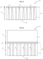
- the assembly 1 or the power semiconductor device 10 shown in Figure 2 is basically identical to the assembly 1 or the power semiconductor device 10 shown in Figure 1A with the exception that Figure 2 shows only four vias 1V.
- the assembly 1 or the power semiconductor device 10 shown in Figure 3 is basically identical to the assembly 1 or the power semiconductor device 10 shown in Figure 1A with the exception that the vias 1V have cross sections whose sizes vary along the vertical direction.
- the size of the cross section of each of the vias 1V increases with decreasing distance to the bottom side 11B of the first layer 11.
- inner walls of the vias 1V may be sloped in order to facilitate metallization for instance at the end of semiconductor processing.
- each of the vias 1V has the largest cross section or the largest opening. This simplifies the filling of the material of the vias 1V and can ensure that the vias 1V can be fully filled with an electrical material like aluminium, copper, silver or the like.
- the assembly 1 or the power semiconductor device 10 shown in Figure 4 is basically identical to the assembly 1 or the power semiconductor device 10 shown in Figure 1A with the exception that a substrate 5 is arranged on the main body 1M.
- the substrate 5 and the main body 1M can have the same geometrical sizes, for instance the same length, width and thickness. It is also possible for the substrate 5 to have smaller or greater vertical thickness 5T than the main body 1M.
- the substrate 5 can be formed from SiC.
- the substrate 5 is formed from the same material as the first layer 11 of the main body 1M.
- the second layer 12 is arranged between the SiC substrate 5 and the first layer 11.
- the substrate 5 has a vertical thickness 5T, wherein a ratio 5T/12T of the substrate 5 to the second thickness 12T can be from 1.5 to 250, for instance from 5 to 250, from 5 to 200, from 5 to 100, from 5 to 50, from 5 to 25, from 5 to 25.
- the ratio 5T/12T is larger or equal 5, 10, 30, 50 or 100.
- the ratio 5T/12T is larger than or equal 1.5 and 5 but can be smaller or equal 10, 15, 20, 30, 50 or 100.
- a ratio 5T/11T of the substrate 5 to the first thickness 11T can be from 0.3 to 3, for instance from 0.5 to 3, from 1 to 3, from 0.5 to 2, from 0.5 to 1.5, from 0.75 to 1.25, from 0.8 to 1.2 or from 0.9 to 1.1.
- the substrate 5 is void of any vias formed from an electrically conductive material.
- the substrate 5 may act as a top-side cooler.
- the substrate 5 and the main body 1M may be separated by a metal layer, for instance an aluminium or a copper layer, which may constitute an electrode, for instance a cathode of the assembly 1 or of the power semiconductor device 10.
- the substrate 5 acting as a top-side cooler is not electrically active. For this reason, no vias, holes or trenches are required for reducing a resistive voltage drop.
- a thermal boundary electrode can be present at a bottom side of the assembly 1 or of the power semiconductor device 10, for example at the bottom side 11B of the first layer 11 of the main body 1M.
- the assembly 1 or the power semiconductor device 10 shown in Figure 5 is basically identical to the assembly 1 or the power semiconductor device 10 shown in Figure 1A with the exception that the main body 1M is arranged on a heat sink 3.
- the heat sink 3 can be formed from a metal, for instance from copper.
- the heat sink 3 has a vertical thickness 3T which is larger than a sum of the first thickness 11T and the second thickness 12T, for instance at least 1.5, 2, 3 or 5 times larger than a sum of the first thickness 11T and the second thickness 12T.
- the heat sink 3 acts as a main heat sink or as a main cooler of the assembly 1 or of the power semiconductor device 10.
- the presence of the heat sink 3 results in a reduction of self-heating and improvement of current density. These effects are enhanced if the heat sink 3 is used in combination with the vias 1V formed in the first layer 11.
- the main body 1M and the heat sink 3 may have substantially the same geometrical sizes with regard to lateral length and/or lateral width.
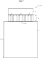
- the assembly 1 or the power semiconductor device 10 shown in Figure 6 is basically identical to the assembly 1 or the power semiconductor device 10 shown in Figure 5 with the exception that heat sink 3 has a larger cross section than the main body 1M.
- the main body 1M can fully overlap with the heat sink 3.
- the lateral length and the lateral width of the heat sink 3 are larger than the lateral length and the lateral width of the main body 1M, respectively.
- the heat sink 3 shown in Figure 5 and the heat sink shown in Figure 6 may have the same volume. It has been found out that compared to the heat sink 3 shown in Figure 5 , the use of the heat sink 3 shown in Figure 6 results in further reduction of self-heating and improvement of current density.
- the assembly 1 or the power semiconductor device 10 shown in Figure 7 is basically identical to the assembly 1 or the power semiconductor device 10 shown in Figure 4 with the exception that the assembly 1 or the power semiconductor device 10 shown in Figure 7 comprises a heat sink 3 as shown in Figure 6 .
- a procedure to manufacture SiC power devices can depart with the first layer 11 being a thick and highly doped SiC layer.
- the second layer 12 being a thin, lowly doped voltage sustaining SiC drift layer, can be epitaxially grown on top of the first layer 11.
- the thickness of the drift layer may range from a few um up to about 10 um for the voltage classes mentioned above which is very thin compared to the thick first layer 11 having a vertical thickness 11T of 100 um, 200 um, 300 um or more.
- the thickness of the first layer 11 will be thinned in order to allow the minimum on-state voltage drop to be reached.
- this assembly 1 or this power semiconductor device 10 being for instance a resistor has two electrical contacts used to energize the arrangement. Since aluminium is widely used for metal contacts in power semiconductor devices, the simulated contacts are chosen to be formed from aluminium.
- An initial temperature is set to be 300 K in this example and the thermal electrode is characterized by a thermal surface resistance of 10 cm 2 K/W. This value of the thermal surface resistance is exemplary of mounting the power semiconductor device on a small heat sink without forced cooling.
- a surface temperature of the thermal boundary of 300 K is used.
- a current pulse of a length of 3 seconds is subjected onto the assembly 1 or the power semiconductor device 10 comprising the first layer 11 and the second layer 12.
- the height of the current density pulse is variable and will thus yield different maximum device temperatures at the end of the current pulse.
- a typical conventional thickness of the first SiC layer 11 is chosen to be 100 um and a typical conventional thickness of the second SiC layer 12 being a drift layer is chosen to be 8 um with a resistance typical for a 1.2 kV SiC JFET with 1.4 m ⁇ cm 2 on-resistance on top of the first layer 11.
- the width of the first layer 11 and of the second layer is chosen to be 5120 um and a current of variable height is impressed through the second layer 12 and the first layer 11 flowing from top to bottom of the assembly 1.
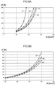
- Curve A2 corresponds to the same configuration of the assembly 1 or of the power semiconductor device 10 as for curve A1 but with a first layer 11 having a thickness 11T of 600 um without any vias 1V.
- Curve A3 corresponds to the same configuration of the assembly 1 or of the power semiconductor device 10 as for curve A2 but with four vias 1V as shown in Figure 2 .
- each of the four vias 1V is in the form of trench having a lateral width of 40 um and a vertical height of 590 um which is assumed to be filled with copper. They provide an electrical bypass from the second layer 12 being a drift layer at the top to an electrical contact at the bottom side 11B of the first layer 11.
- a thermal boundary/electrode is also located at the bottom side 11B of the first layer 11.
- Curve A4 corresponds to the same configuration of the assembly 1 or of the power semiconductor device 10 as for curve A2 but with eight vias 1V as shown in Figure 1A .
- each of the eight vias 1V is in the form of trench having a lateral width of 20 um and a vertical height of 590 um which is assumed to be filled with copper. They provide an electrical bypass from the second layer 12 being a drift layer at the top to an electrical contact at the bottom side 11B of the first layer 11.
- a thermal boundary/electrode is also located at the bottom side 11B of the first layer 11.
- the thicker first layer 11 adds a fair amount of heat capacity. This will lead to a slower increase of the assembly temperature when the current pulse is applied. It has been also observed that there is, however, a second opposed effect taking place, namely: when the thickness 11T of the first layer is increased, the total resistance of the assembly 1 or of the power semiconductor device 10 will become higher. This means that the heat generation caused by the very same current pulse will be higher in the second case. Accordingly, there will be a maximum thickness 11T of the first layer 11, where the final maximum temperature reached after the current pulse will no longer decrease, instead, it will increase again.
- the top of the vias 1V may stop short in front of the second layer 12, for instance in the range of the 1 um to 50 um, here 10 um in the case of curves A3 and A4, thereby contributing a maximum path to bypass the resistance of the first layer 11.
- the width of the four vias 1V in case of the curve A3 and the width of the eight vias 1V in case of the curve A4 are chosen to be different on purpose: it shows that the width of the vias 1V and the lateral spacing between the vias 1V is a suitable parameter to optimize. Results of self-heating simulations for various configurations are provided by the curves A1 to A4.
- Figure 8B shows further curves B1, B2 and B3 as a function of temperature increase depending on the current density after 3-second current pulse.
- Curve B1 corresponds to the same configuration of the assembly 1 or of the power semiconductor device 10 comprising a first SiC layer 11 having a thickness 11T of 600 um without any vias 1V, a second SiC layer 12 being a drift layer having a thickness of 8 um and further configuration of the assembly 1 or of the power semiconductor device 10 according to curve A2.
- the assembly 1 or of the power semiconductor device 10 is arranged on a heat sink 3 being copper plate having a thickness 3T of 4180 um.
- Such an assembly 1 or a power semiconductor device 10 is shown in Figure 5 , but without any vias 1V in the first layer 11.
- Curve B2 corresponds to the same configuration of the assembly 1 or of the power semiconductor device 10 as for curve B1 but with a first SiC layer 11 having a thickness 11T of 600 um and four vias 1V as shown in Figure 2 .
- Such an assembly 1 or a power semiconductor device 10 is shown in Figure 5 , but with four vias 1V in the first layer 11, wherein each of the four vias 1V is in the form of trench having a lateral width of 40 um and a vertical height of 590 um and is filled with copper.
- Curve B3 corresponds to the same configuration of the assembly 1 or of the power semiconductor device 10 as for curve B1 but with eight vias 1V.
- Such an assembly 1 or a power semiconductor device 10 is shown in Figure 5 with eight vias 1V in the first layer 11, wherein each of the eight vias 1V is in the form of trench having a lateral width of 20 um and a vertical height of 590 um and is filled with copper.
- Figure 8B also shows that the benefit of the thick SiC first layer 11 featuring the vias 1V filled with copper continues to be significant albeit at higher current densities, for instance at 300 A/cm 2 . At lower current densities, for instance at 150 A/cm 2 , the tolerable maximum current density is increased by 10 % or more.
- Figure 8C shows curves B1, B2 and B3 already shown in Figure 8B and additional curves C4 and C5.
- Curve C4 corresponds to the same configuration of the assembly 1 or of the power semiconductor device 10 as for curve B3 but with a heat sink 3 which exceeds the width or the cross section of the main body 1M as shown in Figure 6 .
- the sizes of the heat sink 3 has been changed from 5120 ⁇ m x 4180 um to 10240 ⁇ m x 2090 um, wherein the volume of the heat sink 3 remains unchanged.
- the heat sink 3 in Figure 6 has a larger width or larger cross section but a smaller thickness 3T.
- the volume of the heat sink 3 shown in Figure 5 and the volume of the heat sink 3 shown in Figure 6 can be the same, which is the case for the configuration of the assembly 1 or of the power semiconductor device 10 according to curves B3 and C4.
- curve B3 corresponds to of the assembly 1 or of the power semiconductor device 10 shown in Figure 5
- curve C4 corresponds to the assembly 1 or the power semiconductor device 10 shown in Figure 5 .
- Curve C5 corresponds to the same configuration of the assembly 1 or of the power semiconductor device 10 as for curve C4 with the exception that the assembly 1 or the power semiconductor device 10 comprises a SiC substrate 5, i.e. a top-side cooler, as shown in Figure 7 .
- the SiC substrate 5 can have roughly the same sizes as the first layer 11 or the main body 1M.
- the substrate 5, however, is free of vias 1V.
- the SiC substrate and the first SiC layer 11 have the same thickness of 600 um.
- Figure 8D is basically identical to Figure 8A , wherein in Figure 8D , an additional curve D5 is shown.
- the curve D5 corresponds to the same configuration of the assembly 1 or of the power semiconductor device 10 as for curve A4 as shown in Figure 1A with the exception that the assembly 1 comprises the further SiC substrate 5 having the thickness 5T as shown in Figure 4 .
- the thickness 5T is chosen to be 600 um.
- Curve D5 shows that the further substrate 5 can retard thermal runaway further, resulting in a further reduction of self-heating and further improvement of current density.
- FIG 8A to 8D some main ideas of this disclosure have been illustrated for a 1200 V device. This can be extended to other voltage classes to achieve similar benefit in lowering the device temperature, thereby increasing the operating current density. The benefit could be more evident in low voltage class like a 600 V device, typically used in an event switching application, as the contribution from the thick first layer 11 towards the total device resistance is more at such voltage range.
- the illustrations have been made using a 600 um thick first SiC layer 11. This could be applied to a standard SiC first layer 11 acting as a substrate having a thickness 11T of about 350 um, where a similar trend in benefit would be observed by using metal filled trenches or vias 1V in the first layer 11 and/or in combination with the heat sink 3 and the further substrate 5.
- Figures 9A, 9B and 9C show some exemplary method steps of a method for producing at least one assembly 1 for a power semiconductor device 10.
- a wafer 100 comprising at least one main body 1M based on SiC
- the main body 1M comprises a first layer 11 having a first thickness 11T and a second layer 12 having a second thickness 12T.
- the second thickness 12T is smaller than the first thickness 11T, wherein the first layer 11 and the second layer 12 are formed from SiC.
- the first layer 11 has a higher n-doping concentration than the second layer 12.
- the first layer 11 is formed as a substrate and the second layer 12 as a drift layer of the assembly 1 or of the power semiconductor device 10.
- a plurality of trenches 1H extending along a vertical direction from a bottom side 11B of the first layer 11 partially into the first layer 11 towards the second layer 12, wherein the trenches 1H do not extend into the second layer 12.
- the trenches 1H can be formed by a drilling and/or etching process.
- the trenches 1H are filled with an electrically conductive material for forming a plurality of vias 1V, wherein the vias 1V extend along the vertical direction from the bottom side 11B of the first layer 11 partially into the first layer 11 towards the second layer 12 and do not extend into the second layer 12.
- the vias 1V do not provide a connection between the bottom side 11B and a top side of the first layer 11.
- the trenches 1H are not formed as through-holes extending throughout the first layer 11 along the vertical direction.
- the vias 1V are not formed as through-vias.
- the trenches 1H can be fully filed with the electrically conductive material as shown in Figure 9C . It is, however, possible that the trenches 1H are partly filled with the electrically conductive material. For instance, only inner walls of the trenches 1H are covered with the electrically conductive material. In this case the trenches 1H may comprise regions which are filled with a gaseous medium, for instance with air.
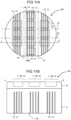
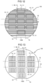
- Figure 10A shows a possible arrangement of the trenches 1H or of the vias 1V relative to an edge 100E of the wafer 100 and relative the plurality of the to-be-produced assemblies 1 or power semiconductor devices 10.
- the trenches 1H or vias 1V extend orthogonal to the edge 100E. In a top view on a bottom side of the wafer, some of the trenches 1H or vias 1V overlap with a plurality of the to-be-produced assemblies 1 or power semiconductor devices 10.
- the trenches 1H or the vias 1V are parallel to each other.
- the trenches 1H or the vias 1V can also be formed in regions between the to-be-produced assemblies 1 or power semiconductor devices 10.
- the trenches 1H or the vias 1V can extend over the entire lateral expansion of the wafer 100.
- Figure 10B show a sectional view of the wafer 100 as shown in Figure 10A along the line AB.
- other lateral orientations of the trenches 1H or of the vias 1V are also possible.
- the trenches 1H or of the vias 1V are parallel to the edge 100E of the wafer, or can form an acute with the edge 100E.
- the wafer 100 shown in Figure 11A is basically identical to the wafer 100 with the trenches 1H or vias 1V shown in Figure 10A with the exception that there are no trenches 1H or vias 1V located in regions between the to-be-produced assemblies 1 or power semiconductor devices 10. Thus, it can be ensured that some of the singulating lines do not cut through the trenches 1H or vias 1V.
- Figure 11B show a sectional view of the wafer 100 as shown in Figure 11A along the line AB.
- the wafer 100 shown in Figure 12 is basically identical to the wafer 100 with the trenches 1H or vias 1V shown in Figure 10A with the exception that the trenches 1H or vias 1V are parallel to the edge 100E of the wafer.
- the wafer 100 shown in Figure 13 is basically identical to the wafer 100 with the trenches 1H or vias 1V shown in Figure 10A with the exception that the trenches 1H or vias 1V are formed only in the regions of the to-be-produced assemblies 1 or power semiconductor devices 10. Thus, in lateral directions, the trenches 1H or vias 1V are fully surrounded by the first layer 11.
- the vias 1V are rotated by an angle of 90° or by another angle, for instance by an angle of 45° ⁇ 10°, 45° ⁇ 15°, 45° ⁇ 20° or 45° ⁇ 30°.
- the vias 1V in top view on the bottom side of the first layer 11, can extend over the entire lateral width or the lateral length of the to-be-produced power semiconductor devices 10.
- the vias 1V can also have a lateral expansion which is smaller than the lateral width and smaller than the lateral length of the to-be-produced power semiconductor devices 10.
- the vias 1V can have a lateral expansion which is larger than the lateral width and/or the lateral length of the to-be-produced power semiconductor devices 10.
Landscapes
- Electrodes Of Semiconductors (AREA)
Abstract
An assembly (1) for a power semiconductor device (10) is provided, wherein
- the assembly (1) comprises a main body (1M) based on SiC and a plurality of vias (1V) based on an electrically conductive material,
- the main body (1M) comprises a first layer (11) having a first thickness (11T) and a second layer (12) having a second thickness (12T), the second thickness (12T) being smaller than the first thickness (11T),
- the first layer (11) and the second layer (12) are formed from SiC, the first layer (11) having a higher n-doping concentration than the second layer (12), and
- the vias (1V) extend along a vertical direction from a bottom side (11B) of the first layer (11) partially into the first layer (11) towards the second layer (12), the vias (1V) not extending into the second layer (12).
- the assembly (1) comprises a main body (1M) based on SiC and a plurality of vias (1V) based on an electrically conductive material,
- the main body (1M) comprises a first layer (11) having a first thickness (11T) and a second layer (12) having a second thickness (12T), the second thickness (12T) being smaller than the first thickness (11T),
- the first layer (11) and the second layer (12) are formed from SiC, the first layer (11) having a higher n-doping concentration than the second layer (12), and
- the vias (1V) extend along a vertical direction from a bottom side (11B) of the first layer (11) partially into the first layer (11) towards the second layer (12), the vias (1V) not extending into the second layer (12).
Moreover, a power semiconductor device (10) comprising such an assembly (1) and a method for producing such an assembly (1) and a method are provided.
Description
- The present disclosure relates to a SiC assembly, a power semiconductor device and a method for producing a SiC assembly for a power semiconductor device.
- Conventional low voltage SiC devices provide very low on-state voltage drop required by certain applications such as event switching applications. However, switches shall withstand high current pulses for an extended lapse of time ranging from few µs to few seconds. This puts high demands on the so-called "single event" turn-off capability not only because of high turn-off current densities and/or long pulse lengths but also because of very high temperature swings of the whole switch affecting both the chip and the package.
- The realm of recent SiC technology and material properties complicates this situation since current die sizes are limited to typical values for instance not exceeding 50 mm2 because of the crystal defect densities and their limiting effect on production yield and therefore die cost. In the present situation, it is thus desired to fully optimize the potential of SiC devices, for instance SiC switches regarding the on-resistance. Thus, for keeping the SiC die area as low as possible for economic reasons, current densities under normal operating conditions shall be pushed as high as possible. This, however, results in extremely high current densities during the high current event leading to intense self-heating of the semiconductor chip and its package. While the semiconductor material SiC is very well able to operate at high temperatures, under vacuum at up to 600 K or higher, state-of-the-art packages and the materials used to make them will not allow to exceed maximum operating temperatures for silicon devices by much. In the case of SiC device, which are used for instance in event switching applications, there is thus a strong interest to add heat capacity to the device as much as possible. This disclosure intends to reach this goal by making use of a highly heat conductive SiC layer on which for instance a voltage sustaining drift layer of a power semiconductor device, for example of a switch device, is applied or grown.
- Embodiments of the disclosure, for instance as claimed in the independent claims, address the above shortcomings in the art in whole or in part. Further embodiments of the SiC assembly, the power semiconductor device and as well as of the method for producing a SiC assembly for a power semiconductor device are subject-matter of the further claims.
- According to an embodiment of an assembly for a power semiconductor device, it comprises a main body based on SiC and a plurality of vias based on an electrically conductive material. The main body comprises a first layer having a first thickness and a second layer having a second thickness, wherein the second thickness is smaller than the first thickness. The first layer and the second layer are formed from SiC. The first layer can have a higher n-doping concentration than the second layer. The vias extend along a vertical direction from a bottom side of the first layer partially into the first layer towards the second layer, wherein the vias do not extend into the second layer.
- The first layer and the second layer have different n-doping concentration. However, the first layer and the second layer may be formed from the same material, for instance from 4H-SiC. It is, however, possible that the second layer is formed from 4H-SiC, and the first layer is formed from 3C-SiC or poly-SiC. For instance, the second layer is a drift layer. Such a drift layer can be epitaxially grown on the first layer. The first layer can be a substrate which carries the second layer and mechanically stabilizes the assembly.
- The vias can be trenches which are fully filed with the electrically conductive material. It is also possible that the vias can are trenches which are partly filled with the electrically conductive material. For instance, only inner walls of the trenches are covered with the electrically conductive material. In this case the trenches may comprise regions which are filled with a gaseous medium, for instance with air.
- The goal of this disclosure is to make use a thicker first layer allowing reduced self-heating without having the disadvantage of increasing simultaneously a total resistance of an arrangement, for instance of the power semiconductor device. This goal is reached providing holes or trenches in two- or three-dimensional arrangements in the first layer which are filled with a metal with high electrical conductivity and high thermal conductivity, for instance with aluminium, copper or silver due to their high intrinsic electrical conductance or with an appropriate form of graphite. The number of holes or trenches for each assembly may be at least 4, 6, 8, 10, 16, 20, 50 or at least 100. According to a further embodiment of the assembly, a ratio of the vertical first thickness to the vertical second thickness is from 1.5 to 250. The first thickness can be from 100 um to 1000 um. The second thickness can be from 2 um to 200 um.
- A vertical direction is understood to mean a direction which is directed perpendicular to a bottom surface of the first layer. A lateral direction is understood to mean a direction which is parallel to the bottom surface of the first layer. The vertical direction and the lateral direction are orthogonal to each other. The bottom surface of the first layer is located at the bottom side of the first layer and is a lateral surface which can be defined by one vector directing along a length of the assembly and by another vector directing along a width of the assembly.
- According to a further embodiment of the assembly, a maximal vertical distance between the second layer and the vias is from 0.6 um to 250 um, for instance from 1 um to 250 um. For example, the first thickness is larger than or equal 300 um or 350 um. The second thickness is for instance smaller than or equal to 55 um or 25 um or 10 um. The first thickness and the second thickness, however, are not limited thereto.
- According to a further embodiment of the assembly, a ratio of an average vertical height of the vias to the first thickness of the first layer is at least 0.5, for instance at least 0.6, 0.7, 0.8 or at least 0.9. In other words, the vias extend into at least 50%, 60%, 70%, 80% or at least 90% of the total vertical thickness of the first layer. The vias, however, do not extend throughout the first layer along the vertical direction. In this sense, the vias extend along the vertical direction from the bottom side of the first layer only partially into the first layer towards the second layer.
- According to a further embodiment of the assembly, the vias have a lateral average width from 3 um to 150 um, for instance from 6 um to 150 um or from 10 um to 150 um. The vias have a lateral average length which is larger than the lateral average width. Along lateral directions, at least some of the vias or all the vias can be fully or partly enclosed by the first layer. It is possible, however, that along one lateral direction, at least some of the vias or all the vias can extend from one first side surface of the first layer to another side surface of the first layer for instance opposite to the first side surface of the first layer. In this case, the vias can be exposed not only at the bottom side of the first layer but also on at least partially one side surface or on two side surfaces of the first layer.
- According to a further embodiment of the assembly, along lateral directions, the vias are fully surrounded by the first layer. In this case, the vias are not exposed on side surfaces of the first layer.
- According to a further embodiment of the assembly, the first layer has a first side surface and a second side surface. Along lateral direction, at least one, several of vias or all the vias can extend from the first side surface to the second side surface of the first layer. For instance the first side surface is opposite to the second side surface. In this case, it is possible that the vias have lateral lengths which are equal to or larger than a lateral width or a lateral length of the first layer. Along a lateral direction, the vias can extend along the width or along the length of the first layer. It is also possible that the first side surface is adjacent to the second side surface. In this case, along a lateral direction, the vias can extend from the first side surface to the adjacent second side surface. Along a lateral direction, the vias are not parallel to the orientation of the width or the length of the first layer.
- According to a further embodiment of the assembly, it further comprises a heat sink formed for instance from a metal. The main body is arranged on the heat sink, for instance directly on the heat sink. The heat sink has a vertical thickness which is for instance larger than a sum of the first thickness and the second thickness.
- The heat sink can be a thick metal plate, for instance a copper plate, which serves as an efficient main heat sink for the assembly or for the semiconductor device. The heat sink can have sizes of the same width and/or length of the main body. A vertical thickness of the heat sink can be equal to or larger than 500 um, 1000 µm, 2000 um, 3000 um or 4000 um.
- According to a further embodiment of the assembly, the heat sink has a larger cross section than the main body so that in a top view of the heat sink, the main body fully overlaps with the heat sink. It is, however, also possible for the heat sink to have equal or roughly equal cross section compared to the cross section of the main body.
- According to a further embodiment of the assembly, it further comprises a SiC substrate, wherein the second layer is arranged between the SiC substrate and the first layer. The SiC substrate has a vertical thickness, wherein a ratio of the SiC substrate to the second thickness being can be from 1.5 to 250. The SiC substrate is for instance void of any vias formed from an electrically conductive material.
- The SiC substrate and the main body may be separated by a metal layer, for instance an aluminium layer or a copper layer, which can constitute an electrode, for instance a cathode of the assembly or of the power semiconductor device. The SiC substrate acts as a top-side cooler and is for instance not electrically active. For this reason, no vias, holes or trenches are formed within the SiC for reducing possible resistive voltage drop. For instance, a thermal boundary electrode is present at the bottom side of the assembly.
- According to a further embodiment of the assembly, the vias have cross sections whose sizes vary along the vertical direction. For instance, the size of the cross section of each of the vias increases with decreasing distance from the bottom side of the first layer. Due to this geometry of the vias, the vias can be filled with the electrically conductive material in an efficient and simplified manner.
- According to one embodiment of a power semiconductor device, it comprises an assembly, in particular the assembly described here in this disclosure. The assembly comprises a main body based on SiC and a plurality of vias based on an electrically conductive material. The main body comprises a first layer having a first thickness and a second layer, wherein the second thickness is smaller than the first thickness. The first layer and the second layer are formed from SiC, wherein the first layer has a higher n-doping concentration than the second layer. The vias extend along a vertical direction from a bottom side of the first layer partially into the first layer towards the second layer, wherein the vias do not extend into the second layer. The second layer comprises functional regions configured to carry out functionality of the power semiconductor device. The functional regions can comprise p- and n-regions for instance of a transistor. For instance, the second layer is formed as a drift layer.
- According to a further embodiment of the power semiconductor device, it is formed as a metal-oxide-silicon field-effect transistor (MOSFET), a junction field-effect transistor (JFET), an insulated-gate bipolar transistor (IGBT), a Schottky diode, a Junction Barrier Schottky (JBS) diode or as a SiC power device for event switching. The second layer can comprise the functional regions of such a transistor or diode.
- According to one embodiment of a method for producing an assembly for a power semiconductor device, a wafer is provided. The wafer comprising at least one main body based on SiC. The wafer or the main body comprises a first layer having a first thickness and a second layer having a second thickness, wherein the second thickness is smaller than the first thickness. The first layer and the second layer are formed from SiC. The first layer can have a higher n-doping concentration than the second layer. According to the method, a plurality of trenches are formed which extend along a vertical direction from a bottom side of the first layer partially into the first layer towards the second layer, wherein the trenches do not extend into the second layer. The trenches are filled with an electrically conductive material for forming a plurality of vias, wherein the vias extend along the vertical direction from the bottom side of the first layer partially into the first layer towards the second layer and do not extend into the second layer.
- According to a further embodiment of the method, the wafer is singulated along singulating lines into a plurality of main bodies, wherein at least some of the singulating lines cut through the vias so that at least some of the singulated main bodies comprise side surfaces which comprise side surfaces of the vias.
- According to a further embodiment of the method, the wafer is singulated along singulating lines into a plurality of main bodies, wherein at least some of the singulating lines do not cut through the vias so that at least some of the singulated main bodies comprise all side surfaces being void of side surfaces of the vias.
- The present disclosure comprises several aspects of an assembly for a power semiconductor device, of a power semiconductor device comprising such an assembly and of a method for producing such an assembly for such a power semiconductor device on the basis of their embodiments and examples. Every feature described with respect to one of the aspects is also disclosed herein with respect to the other aspect, even if the respective feature is not explicitly mentioned in the context of the specific aspect. For example, the method described in this disclosure is directed to a method for producing the assembly described here, and the power semiconductor device described in this disclosure can comprise the assembly described here. Thus, features and advantages described in connection with the assembly can be used for the method and for the power semiconductor device, and vice versa.
- While the disclosure is amenable to various modifications and alternative forms, specifics thereof are shown by way of example in the figures and will be described in detail. It should be understood, however, that the intention is not to limit the disclosure to the particular described embodiments and examples. On the contrary, the intention is to cover all modifications, equivalents, and alternatives falling within the scope of the disclosure defined by the appended claims.
- The accompanying figures are included to provide a further understanding. In the figures, elements of the same structure and/or functionality may be assigned to the same reference signs. It is to be understood that the examples shown in the figures are illustrative representations and are not necessarily true to scale.
-
Figure 1A schematically shows a general concept of an assembly for a power semiconductor device in cross-sectional view according to an example of the disclosure. -
Figures 1B and1C show - in top view on a bottom side of the assembly - different arrangements of vias according to different examples of the assembly. -
Figures 2 ,3 ,4 ,5 ,6 and7 show further examples of the assembly or of the power semiconductor device. -
Figure 8A, 8B ,8C and 8D show some simulation results of different examples of the assembly. -
Figures 9A, 9B and 9C show some exemplary method steps of a method for producing at least one assembly for a power semiconductor device. -
Figures 10A, 10B ,11A, 11B ,12 and 13 show some exemplary method steps of different examples for a method for producing a plurality of assemblies for a power semiconductor device. -
Figure 1A shows a sectional view of anassembly 1 for apower semiconductor device 10 according to one exemplary embodiment. Theassembly 1 comprises amain body 1M comprising afirst layer 11 having afirst thickness 11T and asecond layer 12 having asecond thickness 12T. Themain body 1M is based on SiC. Thefirst layer 11 is formed from SiC, for instance from 4H-SiC, 3C-SiC or poly-SiC. Thesecond layer 12 is formed from SiC, for instance from 4H-SiC. Thefirst layer 11 has a higher n-doping concentration than thesecond layer 12. As shown inFigure 1A , thesecond thickness 12T is smaller than thefirst thickness 11T. Thesecond layer 12 can be directly adjacent to thefirst layer 11. - A
ratio 11T/12T of thefirst thickness 11T to thesecond thickness 12T can be from 1.5 to 250, for instance from 5 to 250, from 5 to 200, from 5 to 100, from 5 to 50, from 5 to 25, from 5 to 25. For instance, theratio 11T/12T is larger or equal 5, 10, 30, 50 or 100. For instance, theratio 11T/12T is larger than or equal 1.5 and 5 but can be smaller or equal 10, 15, 20, 30, 50 or 100. - The
first thickness 11T can be from 100 um to 1000 um, for instance from 100 um to 800 um, from 100 um to 600 um, from 100 um to 400 um. For instance, thefirst thickness 11T is 600 µm ± 300 um or 600 µm ± 200 um or 600 µm ± 50 um. - The
second thickness 12T can be from 2 um to 200 um, for instance from 2 um to 100 um, from 2 um to 50 um, from 2 um to 10 um. For instance, thesecond thickness 12T is 50 µm ± 10 um or 30 µm ± 10 um or 10 µm ± 5 µm. - For instance, the
first thickness 11T is larger than or equal 300 um or 500 um, and thesecond thickness 12T is smaller than or equal to 55 um, 35 um, 20 um or 10 um. - The
assembly 1 comprises a plurality ofvias 1V which are based on an electrically conductive material. For instance, thevias 1V are trenches which are filled for instance with aluminium, copper or silver. Thevias 1V extend along a vertical direction from abottom side 11B of thefirst layer 11 partially into thefirst layer 11 towards thesecond layer 12, wherein thevias 1V do not extend into thesecond layer 12 but stop in front of thesecond layer 12. - A maximal vertical distance between the
second layer 12 and thevias 1V can be from 0.6 um to 250 um, for instance from 1 um to 250 um, for instance from 1 um to 150 um, from 1 um to 100 um, from 1 um to 50 um, from 1 um to 30 um or from 1 um to 10 um. - As shown in
Figure 1A , thevias 1V only partially extend into the first layer. It is possible that a ratio of an average vertical height of thevias 1V to thefirst thickness 11T of thefirst layer 11 is at least 0.5, 0.6, 0.7, 0.8 or at least 0.9, for instance between 0.8 and 0.98. - The
vias 1V can have a lateral average width from 3 um to 150 um, for instance from 6 um to 150 um, from 10 um to 150 um, for instance from 10 um to 100 um, from 10 um to 80 um, from 10 um to 60 um, from 10 um to 40 um or from 10 um to 20 um. Thevias 1V can have a lateral average length which is larger than the lateral average width. The lateral of thevias 1V can be the lateral length or lateral width of theassembly 1. - For instance, in a top view on the
bottom side 11B of thefirst layer 11 as shown for instance inFigures 1B and1C , thevias 1V are strip-shaped. Thevias 1V are parallel to each other. A ratio of the lateral length to the lateral width of one via 1V or of thevias 1V can be from 1.5 to 50, 1.5 to 30, 1.5 to 10 or 1.5 to 5. It is also possible that thevias 1V, in a top view on thebottom side 11B of thefirst layer 11, can have another shapes, for instance a square, circular, trapezoidal shape or other regular and irregular shapes. - As shown in
Figure 1A , theassembly 1 comprises a plurality ofvias 1V, for instance eightvias 1V, which - as shown inFigure 1B - extend along a lateral direction from afirst side surface 11F to asecond side surface 11S of thefirst layer 11, wherein thefirst side surface 11F is opposite to thesecond side surface 11S. Hence, thevias 1V can have a lateral length which is equal or roughly equal to a width of thefirst layer 11. On thefirst side surface 11F and/or on thesecond side surface 11S, thevias 1V can be partially exposed. The eightvias 1V are parallel to each other. - In deviation from
Figure 1B , it is possible that thevias 1V are rotated by an angle of 90°. In this case, thevias 1V can have a lateral length which is equal or roughly equal to a length of thefirst layer 11. Other orientations of thevias 1V are also possible. For instance, along a lateral direction, thevias 1V can extend from thefirst side surface 11F or from thesecond side surface 11S to another side surface of thefirst layer 11, wherein the other side surface of the first layer is adjacent to thefirst side surface 11F or to thesecond side surface 11S. - Compared to the
vias 1V inFigure 1B , in a top view on thebottom side 11B of thefirst layer 11, thevias 1V inFigure 1C have the same lateral orientations. Thevias 1V inFigure 1C , however, do not extend to any side surfaces of thefirst layer 11. Thus, in lateral directions, thevias 1V are fully enclosed or fully surrounded by thefirst layer 11. - In deviation from
Figure 1C , it is possible that thevias 1V can have other orientations along the lateral directions, for instance thevias 1V are rotated by an angle of 90° or by another angle. - In deviation from
Figures 1A, 1B and1C , other arrangements and/or other number of thevias 1V are/is also possible. For instance, the number of thevias 1V is larger or smaller than eight, for instance larger than 10, 15, 20, 30, 40 or 50. A combination of thevias 1V as shown inFigures 1B and1C is also possible. In a top view on thebottom side 11B of thefirst layer 11, thevias 1V can be arranged in a matrix-like manner, i.e. can be arranged in a plurality of columns and rows. It is also possible that only one end or both ends of some of thevias 1V are partially exposed on the side surfaces of thefirst layer 11 and someother vias 1V are fully surrounded by thefirst layers 11 and therefore are not exposed on any of the side surfaces of thefirst layer 11. Theassembly 1 or thepower semiconductor device 10 shown inFigure 2 is basically identical to theassembly 1 or thepower semiconductor device 10 shown inFigure 1A with the exception thatFigure 2 shows only fourvias 1V. - The
assembly 1 or thepower semiconductor device 10 shown inFigure 3 is basically identical to theassembly 1 or thepower semiconductor device 10 shown inFigure 1A with the exception that thevias 1V have cross sections whose sizes vary along the vertical direction. The size of the cross section of each of thevias 1V increases with decreasing distance to thebottom side 11B of thefirst layer 11. Here, inner walls of thevias 1V may be sloped in order to facilitate metallization for instance at the end of semiconductor processing. Thus, at thebottom side 11B, each of thevias 1V has the largest cross section or the largest opening. This simplifies the filling of the material of thevias 1V and can ensure that thevias 1V can be fully filled with an electrical material like aluminium, copper, silver or the like. - The
assembly 1 or thepower semiconductor device 10 shown inFigure 4 is basically identical to theassembly 1 or thepower semiconductor device 10 shown inFigure 1A with the exception that asubstrate 5 is arranged on themain body 1M. Thesubstrate 5 and themain body 1M can have the same geometrical sizes, for instance the same length, width and thickness. It is also possible for thesubstrate 5 to have smaller or greatervertical thickness 5T than themain body 1M. Thesubstrate 5 can be formed from SiC. For instance, thesubstrate 5 is formed from the same material as thefirst layer 11 of themain body 1M. - As shown in
Figure 4 , thesecond layer 12 is arranged between theSiC substrate 5 and thefirst layer 11. Thesubstrate 5 has avertical thickness 5T, wherein aratio 5T/12T of thesubstrate 5 to thesecond thickness 12T can be from 1.5 to 250, for instance from 5 to 250, from 5 to 200, from 5 to 100, from 5 to 50, from 5 to 25, from 5 to 25. For instance, theratio 5T/12T is larger or equal 5, 10, 30, 50 or 100. For instance, theratio 5T/12T is larger than or equal 1.5 and 5 but can be smaller or equal 10, 15, 20, 30, 50 or 100. - A
ratio 5T/11T of thesubstrate 5 to thefirst thickness 11T can be from 0.3 to 3, for instance from 0.5 to 3, from 1 to 3, from 0.5 to 2, from 0.5 to 1.5, from 0.75 to 1.25, from 0.8 to 1.2 or from 0.9 to 1.1. Compared to themain body 1M or to thefirst layer 11, thesubstrate 5, however, is void of any vias formed from an electrically conductive material. - The
substrate 5 may act as a top-side cooler. Thesubstrate 5 and themain body 1M may be separated by a metal layer, for instance an aluminium or a copper layer, which may constitute an electrode, for instance a cathode of theassembly 1 or of thepower semiconductor device 10. Thesubstrate 5 acting as a top-side cooler is not electrically active. For this reason, no vias, holes or trenches are required for reducing a resistive voltage drop. A thermal boundary electrode can be present at a bottom side of theassembly 1 or of thepower semiconductor device 10, for example at thebottom side 11B of thefirst layer 11 of themain body 1M. - The
assembly 1 or thepower semiconductor device 10 shown inFigure 5 is basically identical to theassembly 1 or thepower semiconductor device 10 shown inFigure 1A with the exception that themain body 1M is arranged on aheat sink 3. Theheat sink 3 can be formed from a metal, for instance from copper. Theheat sink 3 has avertical thickness 3T which is larger than a sum of thefirst thickness 11T and thesecond thickness 12T, for instance at least 1.5, 2, 3 or 5 times larger than a sum of thefirst thickness 11T and thesecond thickness 12T. - Here, the
heat sink 3 acts as a main heat sink or as a main cooler of theassembly 1 or of thepower semiconductor device 10. The presence of theheat sink 3 results in a reduction of self-heating and improvement of current density. These effects are enhanced if theheat sink 3 is used in combination with thevias 1V formed in thefirst layer 11. As shown inFigure 5 , themain body 1M and theheat sink 3 may have substantially the same geometrical sizes with regard to lateral length and/or lateral width. - The
assembly 1 or thepower semiconductor device 10 shown inFigure 6 is basically identical to theassembly 1 or thepower semiconductor device 10 shown inFigure 5 with the exception thatheat sink 3 has a larger cross section than themain body 1M. In a top view on theheat sink 3, themain body 1M can fully overlap with theheat sink 3. For example, the lateral length and the lateral width of theheat sink 3 are larger than the lateral length and the lateral width of themain body 1M, respectively. Theheat sink 3 shown inFigure 5 and the heat sink shown inFigure 6 may have the same volume. It has been found out that compared to theheat sink 3 shown inFigure 5 , the use of theheat sink 3 shown inFigure 6 results in further reduction of self-heating and improvement of current density. - The
assembly 1 or thepower semiconductor device 10 shown inFigure 7 is basically identical to theassembly 1 or thepower semiconductor device 10 shown inFigure 4 with the exception that theassembly 1 or thepower semiconductor device 10 shown inFigure 7 comprises aheat sink 3 as shown inFigure 6 . - In connection with
Figures 8A, 8B ,8C and 8D , some simulation results are shown. - A procedure to manufacture SiC power devices can depart with the
first layer 11 being a thick and highly doped SiC layer. For example, in the case of SiC unipolar power devices for 600 V and 1.2 kV applications, thesecond layer 12 being a thin, lowly doped voltage sustaining SiC drift layer, can be epitaxially grown on top of thefirst layer 11. The thickness of the drift layer may range from a few um up to about 10 um for the voltage classes mentioned above which is very thin compared to the thickfirst layer 11 having avertical thickness 11T of 100 um, 200 um, 300 um or more. - As the resistance contribution of the
first layer 11 cannot be neglected, for instance at such low voltage class devices, so far the thickness of thefirst layer 11 will be thinned in order to allow the minimum on-state voltage drop to be reached. - For the self-heating simulation, this
assembly 1 or thispower semiconductor device 10 being for instance a resistor has two electrical contacts used to energize the arrangement. Since aluminium is widely used for metal contacts in power semiconductor devices, the simulated contacts are chosen to be formed from aluminium. On thebottom side 11B of thefirst layer 11, there is a metallization being a thermal electrode on which a thermal boundary condition is implied. An initial temperature is set to be 300 K in this example and the thermal electrode is characterized by a thermal surface resistance of 10 cm2K/W. This value of the thermal surface resistance is exemplary of mounting the power semiconductor device on a small heat sink without forced cooling. - In the simulations discussed here, a surface temperature of the thermal boundary of 300 K is used. In the self-heating simulations, a current pulse of a length of 3 seconds is subjected onto the
assembly 1 or thepower semiconductor device 10 comprising thefirst layer 11 and thesecond layer 12. The height of the current density pulse is variable and will thus yield different maximum device temperatures at the end of the current pulse. - For comparison purposes, in 2D-numerical simulations, a typical conventional thickness of the
first SiC layer 11 is chosen to be 100 um and a typical conventional thickness of thesecond SiC layer 12 being a drift layer is chosen to be 8 um with a resistance typical for a 1.2 kV SiC JFET with 1.4 mΩcm2 on-resistance on top of thefirst layer 11. The width of thefirst layer 11 and of the second layer is chosen to be 5120 um and a current of variable height is impressed through thesecond layer 12 and thefirst layer 11 flowing from top to bottom of theassembly 1. Top and bottom surfaces are electrical contacts, wherein at the bottom surface, there is also a thermal contact which carries a thermal boundary condition T = 300 K. - The results for such a
conventional assembly 1 orpower semiconductor device 10 are displayed by the curve A1 inFigure 8A , wherein dT denotes the average temperature increase in Kelvin and dI denotes the pulsed current density in A/cm2. Here, thefirst layer 11 is void of any vias. - Curve A2 corresponds to the same configuration of the
assembly 1 or of thepower semiconductor device 10 as for curve A1 but with afirst layer 11 having athickness 11T of 600 um without anyvias 1V. - Curve A3 corresponds to the same configuration of the
assembly 1 or of thepower semiconductor device 10 as for curve A2 but with fourvias 1V as shown inFigure 2 . Here, each of the fourvias 1V is in the form of trench having a lateral width of 40 um and a vertical height of 590 um which is assumed to be filled with copper. They provide an electrical bypass from thesecond layer 12 being a drift layer at the top to an electrical contact at thebottom side 11B of thefirst layer 11. A thermal boundary/electrode is also located at thebottom side 11B of thefirst layer 11. - Curve A4 corresponds to the same configuration of the
assembly 1 or of thepower semiconductor device 10 as for curve A2 but with eightvias 1V as shown inFigure 1A . Here, each of the eightvias 1V is in the form of trench having a lateral width of 20 um and a vertical height of 590 um which is assumed to be filled with copper. They provide an electrical bypass from thesecond layer 12 being a drift layer at the top to an electrical contact at thebottom side 11B of thefirst layer 11. A thermal boundary/electrode is also located at thebottom side 11B of thefirst layer 11. - As shown in
Figure 8A , because of the good thermal properties of silicon carbide, the thickerfirst layer 11 adds a fair amount of heat capacity. This will lead to a slower increase of the assembly temperature when the current pulse is applied. It has been also observed that there is, however, a second opposed effect taking place, namely: when thethickness 11T of the first layer is increased, the total resistance of theassembly 1 or of thepower semiconductor device 10 will become higher. This means that the heat generation caused by the very same current pulse will be higher in the second case. Accordingly, there will be amaximum thickness 11T of thefirst layer 11, where the final maximum temperature reached after the current pulse will no longer decrease, instead, it will increase again. - In the presence of the
vias 1V, however, the reduction of self-heating and the improvement of current density can be ensured even for relatively thickfirst layer 11. The top of thevias 1V may stop short in front of thesecond layer 12, for instance in the range of the 1 um to 50 um, here 10 um in the case of curves A3 and A4, thereby contributing a maximum path to bypass the resistance of thefirst layer 11. The width of the fourvias 1V in case of the curve A3 and the width of the eightvias 1V in case of the curve A4 are chosen to be different on purpose: it shows that the width of thevias 1V and the lateral spacing between thevias 1V is a suitable parameter to optimize. Results of self-heating simulations for various configurations are provided by the curves A1 to A4. Although the density of thevias 1V remains at low level, here only 4 or 8vias 1V over an assembly width of 5120 um, the results provided by the curves A3 and A4 already demonstrate a potential of peak temperature limitation exceeding 100 K when measured against the base case provided by curve A1, especially at higher current density. The peak temperature could be limited further by increasing the number and/or dimensions ofvias 1V in thefirst layer 11. - Thus, already by using a two-dimensional simulation, the effectiveness of this approach has been demonstrated with the configurations shown in
Figure 1A and2 . It has been shown that thickfirst layer 11 having a plurality of vias 1V can retard thermal runaway considerably. For enhance this effect, the density of vias 1V per area can be much higher than that used in the numerical examples presented here. -
Figure 8B shows further curves B1, B2 and B3 as a function of temperature increase depending on the current density after 3-second current pulse. - Curve B1 corresponds to the same configuration of the
assembly 1 or of thepower semiconductor device 10 comprising afirst SiC layer 11 having athickness 11T of 600 um without anyvias 1V, asecond SiC layer 12 being a drift layer having a thickness of 8 um and further configuration of theassembly 1 or of thepower semiconductor device 10 according to curve A2. In addition, theassembly 1 or of thepower semiconductor device 10 is arranged on aheat sink 3 being copper plate having athickness 3T of 4180 um. Such anassembly 1 or apower semiconductor device 10 is shown inFigure 5 , but without anyvias 1V in thefirst layer 11. - Curve B2 corresponds to the same configuration of the
assembly 1 or of thepower semiconductor device 10 as for curve B1 but with afirst SiC layer 11 having athickness 11T of 600 um and fourvias 1V as shown inFigure 2 . Such anassembly 1 or apower semiconductor device 10 is shown inFigure 5 , but with fourvias 1V in thefirst layer 11, wherein each of the fourvias 1V is in the form of trench having a lateral width of 40 um and a vertical height of 590 um and is filled with copper. - Curve B3 corresponds to the same configuration of the
assembly 1 or of thepower semiconductor device 10 as for curve B1 but with eightvias 1V. Such anassembly 1 or apower semiconductor device 10 is shown inFigure 5 with eightvias 1V in thefirst layer 11, wherein each of the eightvias 1V is in the form of trench having a lateral width of 20 um and a vertical height of 590 um and is filled with copper. - As shown in
Figure 8B , using a thick first SiC having the highest density of vias 1V can retard thermal runaway in a most efficient way. This effected is enhanced in the presence of theheat sink 3. According toFigure 8B , maximum temperatures reach after a 3 second current pulse with given current density. Compared toFigure 8A , as shown inFigure 8B , it is apparent that the presence of theheat sink 3 greatly limits the final temperature reached at the end of the current pulse. Here, for a given, allowed temperature increase, the maximum current density can be roughly doubled when a thickcopper heat sink 3 as used in the numerical example is added. This can be seen when comparing the curve A4 inFigure 8A to the curve B3 inFigure 8B , for instance at a temperature increase of 150 K. -
Figure 8B also shows that the benefit of the thick SiCfirst layer 11 featuring thevias 1V filled with copper continues to be significant albeit at higher current densities, for instance at 300 A/cm2. At lower current densities, for instance at 150 A/cm2, the tolerable maximum current density is increased by 10 % or more. -
Figure 8C shows curves B1, B2 and B3 already shown inFigure 8B and additional curves C4 and C5. - Curve C4 corresponds to the same configuration of the
assembly 1 or of thepower semiconductor device 10 as for curve B3 but with aheat sink 3 which exceeds the width or the cross section of themain body 1M as shown inFigure 6 . Here, the sizes of theheat sink 3 has been changed from 5120 µm x 4180 um to 10240 µm x 2090 um, wherein the volume of theheat sink 3 remains unchanged. - Compared to the
heat sink 3 shown inFigure 5 , theheat sink 3 inFigure 6 has a larger width or larger cross section but asmaller thickness 3T. Thus, the volume of theheat sink 3 shown inFigure 5 and the volume of theheat sink 3 shown inFigure 6 can be the same, which is the case for the configuration of theassembly 1 or of thepower semiconductor device 10 according to curves B3 and C4. In other word, curve B3 corresponds to of theassembly 1 or of thepower semiconductor device 10 shown inFigure 5 , and curve C4 corresponds to theassembly 1 or thepower semiconductor device 10 shown inFigure 5 . For a quantitative evaluation of the additional effect with regard to the dimension of theheat sink 3, it could be seen from the curves B3 and C4 that thewider heat sink 3 with the same volume offers a reduction of about 50 K at a current density of 300 A/cm2. - Curve C5 corresponds to the same configuration of the
assembly 1 or of thepower semiconductor device 10 as for curve C4 with the exception that theassembly 1 or thepower semiconductor device 10 comprises aSiC substrate 5, i.e. a top-side cooler, as shown inFigure 7 . TheSiC substrate 5 can have roughly the same sizes as thefirst layer 11 or themain body 1M. Thesubstrate 5, however, is free of vias 1V. For the simulation, the SiC substrate and thefirst SiC layer 11 have the same thickness of 600 um. -
Figure 8D is basically identical toFigure 8A , wherein inFigure 8D , an additional curve D5 is shown. The curve D5 corresponds to the same configuration of theassembly 1 or of thepower semiconductor device 10 as for curve A4 as shown inFigure 1A with the exception that theassembly 1 comprises thefurther SiC substrate 5 having thethickness 5T as shown inFigure 4 . For numerical simulation, thethickness 5T is chosen to be 600 um. Curve D5 shows that thefurther substrate 5 can retard thermal runaway further, resulting in a further reduction of self-heating and further improvement of current density. - With the
further SiC substrate 5 being a SiC top-side cooler acting as additional heatsink, final maximum temperatures after completion of the current pulse with a pulse width of 3 seconds can be reduced further. The investigated configuration using a 1.2 kV JFET with 1.4 mΩcm2 on-resistance would endure current pulses at 150 to 160 A/cm2 resulting in a final temperature increase of 150 K. The initial configuration as for curve A1 would reach this temperature increase after a current pulse with 70 to 80 A/cm2. It is clear that the configuration as shown inFigure 4 may be extended for top and/or bottom cooling, i.e. may be extend for thefurther substrate 5 and/or theheat sink 3. In this case, it is possible for thefurther substrate 5 to receive a second thermal boundary/electrode. - In
Figure 8A to 8D , some main ideas of this disclosure have been illustrated for a 1200 V device. This can be extended to other voltage classes to achieve similar benefit in lowering the device temperature, thereby increasing the operating current density. The benefit could be more evident in low voltage class like a 600 V device, typically used in an event switching application, as the contribution from the thickfirst layer 11 towards the total device resistance is more at such voltage range. The illustrations have been made using a 600 um thickfirst SiC layer 11. This could be applied to a standard SiCfirst layer 11 acting as a substrate having athickness 11T of about 350 um, where a similar trend in benefit would be observed by using metal filled trenches orvias 1V in thefirst layer 11 and/or in combination with theheat sink 3 and thefurther substrate 5. -
Figures 9A, 9B and 9C show some exemplary method steps of a method for producing at least oneassembly 1 for apower semiconductor device 10. - According to
Figure 9A , awafer 100 comprising at least onemain body 1M based on SiC is provided, wherein themain body 1M comprises afirst layer 11 having afirst thickness 11T and asecond layer 12 having asecond thickness 12T. Thesecond thickness 12T is smaller than thefirst thickness 11T, wherein thefirst layer 11 and thesecond layer 12 are formed from SiC. Thefirst layer 11 has a higher n-doping concentration than thesecond layer 12. For instance thefirst layer 11 is formed as a substrate and thesecond layer 12 as a drift layer of theassembly 1 or of thepower semiconductor device 10. - According to
Figure 9B , a plurality oftrenches 1H extending along a vertical direction from abottom side 11B of thefirst layer 11 partially into thefirst layer 11 towards thesecond layer 12, wherein thetrenches 1H do not extend into thesecond layer 12. Some possible arrangements of thetrenches 1H are described in connection withFigures 10A to 13 . Thetrenches 1H can be formed by a drilling and/or etching process. - According to
Figure 9C , thetrenches 1H are filled with an electrically conductive material for forming a plurality ofvias 1V, wherein thevias 1V extend along the vertical direction from thebottom side 11B of thefirst layer 11 partially into thefirst layer 11 towards thesecond layer 12 and do not extend into thesecond layer 12. Thus, thevias 1V do not provide a connection between thebottom side 11B and a top side of thefirst layer 11. In other words, thetrenches 1H are not formed as through-holes extending throughout thefirst layer 11 along the vertical direction. Hence, thevias 1V are not formed as through-vias. - The
trenches 1H can be fully filed with the electrically conductive material as shown inFigure 9C . It is, however, possible that thetrenches 1H are partly filled with the electrically conductive material. For instance, only inner walls of thetrenches 1H are covered with the electrically conductive material. In this case thetrenches 1H may comprise regions which are filled with a gaseous medium, for instance with air. -
Figure 10A shows a possible arrangement of thetrenches 1H or of thevias 1V relative to anedge 100E of thewafer 100 and relative the plurality of the to-be-produced assemblies 1 orpower semiconductor devices 10. Thetrenches 1H or vias 1V extend orthogonal to theedge 100E. In a top view on a bottom side of the wafer, some of thetrenches 1H orvias 1V overlap with a plurality of the to-be-produced assemblies 1 orpower semiconductor devices 10. Thetrenches 1H or thevias 1V are parallel to each other. Thetrenches 1H or thevias 1V can also be formed in regions between the to-be-produced assemblies 1 orpower semiconductor devices 10. Thetrenches 1H or thevias 1V can extend over the entire lateral expansion of thewafer 100. - When the
wafer 100 is singulated alongsingulating lines 1S into a plurality ofmain bodies 1M,assemblies 1 orpower semiconductor devices 10, at least some of thesingulating lines 1S cut through thevias 1V so that at least some of the singulatedmain bodies 1M,assemblies 1 orpower semiconductor devices 10 comprise side surfaces which comprise side surfaces of thevias 1V. -
Figure 10B show a sectional view of thewafer 100 as shown inFigure 10A along the line AB. In deviation fromFigures 10A and 10B , other lateral orientations of thetrenches 1H or of thevias 1V are also possible. For example, thetrenches 1H or of thevias 1V are parallel to theedge 100E of the wafer, or can form an acute with theedge 100E. - The
wafer 100 shown inFigure 11A is basically identical to thewafer 100 with thetrenches 1H orvias 1V shown inFigure 10A with the exception that there are notrenches 1H orvias 1V located in regions between the to-be-produced assemblies 1 orpower semiconductor devices 10. Thus, it can be ensured that some of the singulating lines do not cut through thetrenches 1H orvias 1V.Figure 11B show a sectional view of thewafer 100 as shown inFigure 11A along the line AB. - The
wafer 100 shown inFigure 12 is basically identical to thewafer 100 with thetrenches 1H orvias 1V shown inFigure 10A with the exception that thetrenches 1H orvias 1V are parallel to theedge 100E of the wafer. - The
wafer 100 shown inFigure 13 is basically identical to thewafer 100 with thetrenches 1H orvias 1V shown inFigure 10A with the exception that thetrenches 1H orvias 1V are formed only in the regions of the to-be-produced assemblies 1 orpower semiconductor devices 10. Thus, in lateral directions, thetrenches 1H orvias 1V are fully surrounded by thefirst layer 11. - According to
Figure 13 , when thewafer 100 is singulated along thesingulating lines 1S into a plurality ofmain bodies 1M,assemblies 1 orpower semiconductor devices 10, none of thesingulating lines 1S cuts through thevias 1V so that all side surfaces of all singulatedmain bodies 1M,assemblies 1 orpower semiconductor devices 10 are void of thevias 1V. - In deviation from
Figure 13 , it is possible that thevias 1V are rotated by an angle of 90° or by another angle, for instance by an angle of 45° ± 10°, 45° ± 15°, 45° ± 20° or 45° ± 30°. As shown inFigure 13 , in top view on the bottom side of thefirst layer 11, thevias 1V can extend over the entire lateral width or the lateral length of the to-be-producedpower semiconductor devices 10. Thevias 1V can also have a lateral expansion which is smaller than the lateral width and smaller than the lateral length of the to-be-producedpower semiconductor devices 10. In deviation fromFigure 13 , it is also possible that before the step of singulating thewafer 100 into a plurality ofpower semiconductor devices 10, thevias 1V can have a lateral expansion which is larger than the lateral width and/or the lateral length of the to-be-producedpower semiconductor devices 10. - The embodiments shown in the Figures as stated represent exemplary embodiments of an assembly, a power semiconductor device and of a method for producing an assembly for a power semiconductor device; therefore, they do not constitute a complete list of all embodiments according to the improved arrangement for the assembly, power semiconductor device and of the method. Actual arrangements of the assembly, power semiconductor device and of the method may vary from the exemplary embodiments described above.
-
- 100
- wafer
- 10
- power semiconductor device
- 1
- assembly
- 1M
- main body of the assembly
- 1V
- via
- 1H
- trench/ hole
- 1S
- singulating line
- 11
- first layer of the main body
- 11B
- bottom side of the first layer
- 11F
- first side surface of the first layer
- 11S
- second side surface of the first layer
- 11T
- first thickness
- 12
- second layer of the main body
- 12T
- second thickness
- 3
- heat sink
- 3T
- thickness of the heat sink
- 5
- substrate
- 5T
- thickness of the substrate
- 100E
- edge of the wafer
Claims (15)
- An assembly (1) for a power semiconductor device (10) wherein- the assembly (1) comprises a main body (1M) based on SiC and a plurality of vias (1V) based on an electrically conductive material,- the main body (1M) comprises a first layer (11) having a first thickness (11T) and a second layer (12) having a second thickness (12T), the second thickness (12T) being smaller than the first thickness (11T),- the first layer (11) and the second layer (12) are formed from SiC, the first layer (11) having a higher n-doping concentration than the second layer (12), and- the vias (1V) extend along a vertical direction from a bottom side (11B) of the first layer (11) partially into the first layer (11) towards the second layer (12), the vias (1V) not extending into the second layer (12).
- The assembly (1) according to claim 1, wherein- a ratio (11T/12T) of the first thickness (11T) to the second thickness (12T) is from 1.5 to 250,- the first thickness (11T) is from 100 um to 1000 um, and- the second thickness (12T) is from 2 um to 200 um.
- The assembly (1) according to any of the previous claims, wherein- the first thickness (11T) is larger than or equal 300 um,- the second thickness (12T) is smaller than or equal to 55 um, and- a maximal vertical distance between the second layer (12) and the vias (1V) is from 0.6 um to 250 um.
- The assembly (1) according to any of the previous claims, wherein- a ratio of an average vertical height of the vias (1V) to the first thickness (11T) of the first layer (11) is at least 0.5, and- the vias (1V) have a lateral average width between 10 µm and 150 um.
- The assembly (1) according to any of claims 1 to 4, wherein along lateral directions, the vias (1V) are fully surrounded by the first layer (11).
- The assembly (1) according to any of claims 1 to 4, wherein the first layer (11) has a first side surface (11F) and a second side surface (11S), wherein along lateral direction, at least one of vias (1V) extends from the first side surface (11F) to the second side surface (11S).
- The assembly (1) according to any of the previous claims further comprising a heat sink (3) formed from a metal, wherein the main body (1M) is arranged on the heat sink (3), and wherein the heat sink (3) has a vertical thickness (3T) which is larger than a sum of the first thickness (11T) and the second thickness (12T).
- The assembly (1) according to claim 7, wherein heat sink (3) has a larger cross section than the main body (1M) so that in a plan view of the heat sink (3), the main body (1M) fully overlaps with the heat sink (3).
- The assembly (1) according to any of the previous claims further comprising a SiC substrate (5), wherein- the second layer (12) is arranged between the SiC substrate (5) and the first layer (11),- the SiC substrate (5) has a vertical thickness (5T), a ratio (5T/12T) of the SiC substrate (5) to the second thickness (12T) being from 1.5 to 250, and- the SiC substrate (5) is void of any vias formed from an electrically conductive material.
- The assembly (1) according to any of the previous claims, wherein the vias (1V) have cross sections whose sizes vary along the vertical direction, and wherein the size of the cross section of each of the vias (1V) increases with decreasing distance to the bottom side (11B) of the first layer (11).
- A power semiconductor device (10) comprising an assembly (1), wherein- the assembly (1) comprises a main body (1M) based on SiC and a plurality of vias (1V) based on an electrically conductive material,- the main body (1M) comprises a first layer (11) having a first thickness (11T) and a second layer (12), the second thickness (12T) being smaller than the first thickness (11T),- the first layer (11) and the second layer (12) are formed from SiC, the first layer (11) having a higher n-doping concentration than the second layer (12),- the vias (1V) extend along a vertical direction from a bottom side (11B) of the first layer (11) partially into the first layer (11) towards the second layer (12), the vias (1V) not extending into the second layer (12), and- the second layer (12) comprises functional regions configured to carry out functionality of the power semiconductor device (10).
- The power semiconductor device (10) according to claim 11 which is a MOSFET, JFET, IGBT, Schottky diode, a Junction Barrier Schottky diode or a SiC power device for event switching.
- A method for producing an assembly (1) for a power semiconductor device (10) comprising:- providing a wafer (100) comprising at least one main body (1M) based on SiC, wherein the main body (1M) comprises a first layer (11) having a first thickness (11T) and a second layer (12) having a second thickness (12T), the second thickness (12T) is smaller than the first thickness (11T), the first layer (11) and the second layer (12) are formed from SiC, and the first layer (11) has a higher n-doping concentration than the second layer (12),- forming a plurality of trenches (1H) extending along a vertical direction from a bottom side (11B) of the first layer (11) partially into the first layer (11) towards the second layer (12), wherein the trenches (1H) do not extend into the second layer (12), and- filling trenches (1H) with an electrically conductive material for forming a plurality of vias (1V), wherein the vias (1V) extend along the vertical direction from the bottom side (11B) of the first layer (11) partially into the first layer (11) towards the second layer (12) and do not extend into the second layer (12).
- The method according to claim 13, wherein- the wafer (100) is singulated along singulating lines (1S) into a plurality of main bodies (1M), and- at least some of the singulating lines (1S) cut through the vias (1V) so that at least some of the singulated main bodies (1M) comprise side surfaces which comprise side surfaces of the vias (1V).
- The method according to claim 13, wherein- the wafer (100) is singulated along singulating lines (1S) into a plurality of main bodies (1M), and- at least some of the singulating lines (1S) do not cut through the vias (1V) so that at least some of the singulated main bodies (1M) comprise all side surfaces being void of side surfaces of the vias (1V).
Priority Applications (5)
| Application Number | Priority Date | Filing Date | Title |
|---|---|---|---|
| EP23160696.3A EP4428915A1 (en) | 2023-03-08 | 2023-03-08 | Sic assembly, power semiconductor device and method for producing a sic assembly for a power semiconductor device |
| US19/163,209 US20260123370A1 (en) | 2023-03-08 | 2024-02-21 | SiC ASSEMBLY, POWER SEMICONDUCTOR DEVICE AND METHOD FOR PRODUCING A SiC ASSEMBLY FOR A POWER SEMICONDUCTOR DEVICE |
| CN202480017598.7A CN120898290A (en) | 2023-03-08 | 2024-02-21 | SiC components, power semiconductor devices, and methods for manufacturing SiC components for power semiconductor devices. |
| JP2025552040A JP2026507275A (en) | 2023-03-08 | 2024-02-21 | SiC assembly, power semiconductor device and method for manufacturing a SiC assembly of a power semiconductor device |
| PCT/EP2024/054351 WO2024184069A1 (en) | 2023-03-08 | 2024-02-21 | SiC ASSEMBLY, POWER SEMICONDUCTOR DEVICE AND METHOD FOR PRODUCING A SiC ASSEMBLY FOR A POWER SEMICONDUCTOR DEVICE |
Applications Claiming Priority (1)
| Application Number | Priority Date | Filing Date | Title |
|---|---|---|---|
| EP23160696.3A EP4428915A1 (en) | 2023-03-08 | 2023-03-08 | Sic assembly, power semiconductor device and method for producing a sic assembly for a power semiconductor device |
Publications (1)
| Publication Number | Publication Date |
|---|---|
| EP4428915A1 true EP4428915A1 (en) | 2024-09-11 |
Family
ID=85569670
Family Applications (1)
| Application Number | Title | Priority Date | Filing Date |
|---|---|---|---|
| EP23160696.3A Pending EP4428915A1 (en) | 2023-03-08 | 2023-03-08 | Sic assembly, power semiconductor device and method for producing a sic assembly for a power semiconductor device |
Country Status (5)
| Country | Link |
|---|---|
| US (1) | US20260123370A1 (en) |
| EP (1) | EP4428915A1 (en) |
| JP (1) | JP2026507275A (en) |
| CN (1) | CN120898290A (en) |
| WO (1) | WO2024184069A1 (en) |
Citations (3)
| Publication number | Priority date | Publication date | Assignee | Title |
|---|---|---|---|---|
| US20050070048A1 (en) * | 2003-09-25 | 2005-03-31 | Tolchinsky Peter G. | Devices and methods employing high thermal conductivity heat dissipation substrates |
| JP2006156658A (en) * | 2004-11-29 | 2006-06-15 | Toshiba Corp | Semiconductor device |
| JP2013201413A (en) * | 2012-02-21 | 2013-10-03 | Rohm Co Ltd | Semiconductor device and method of manufacturing semiconductor device |
Family Cites Families (3)
| Publication number | Priority date | Publication date | Assignee | Title |
|---|---|---|---|---|
| US5396403A (en) * | 1993-07-06 | 1995-03-07 | Hewlett-Packard Company | Heat sink assembly with thermally-conductive plate for a plurality of integrated circuits on a substrate |
| JP2017059566A (en) * | 2015-09-14 | 2017-03-23 | トヨタ自動車株式会社 | Semiconductor module |
| JP2020009974A (en) * | 2018-07-11 | 2020-01-16 | 北川工業株式会社 | Heat transfer composition |
-
2023
- 2023-03-08 EP EP23160696.3A patent/EP4428915A1/en active Pending
-
2024
- 2024-02-21 CN CN202480017598.7A patent/CN120898290A/en active Pending
- 2024-02-21 JP JP2025552040A patent/JP2026507275A/en active Pending
- 2024-02-21 WO PCT/EP2024/054351 patent/WO2024184069A1/en not_active Ceased
- 2024-02-21 US US19/163,209 patent/US20260123370A1/en active Pending
Patent Citations (3)
| Publication number | Priority date | Publication date | Assignee | Title |
|---|---|---|---|---|
| US20050070048A1 (en) * | 2003-09-25 | 2005-03-31 | Tolchinsky Peter G. | Devices and methods employing high thermal conductivity heat dissipation substrates |
| JP2006156658A (en) * | 2004-11-29 | 2006-06-15 | Toshiba Corp | Semiconductor device |
| JP2013201413A (en) * | 2012-02-21 | 2013-10-03 | Rohm Co Ltd | Semiconductor device and method of manufacturing semiconductor device |
Also Published As
| Publication number | Publication date |
|---|---|
| US20260123370A1 (en) | 2026-04-30 |
| CN120898290A (en) | 2025-11-04 |
| JP2026507275A (en) | 2026-02-27 |
| WO2024184069A1 (en) | 2024-09-12 |
Similar Documents
| Publication | Publication Date | Title |
|---|---|---|
| JP7131003B2 (en) | semiconductor equipment | |
| US6104062A (en) | Semiconductor device having reduced effective substrate resistivity and associated methods | |
| US20070210350A1 (en) | Power semiconductor device, method for manufacturing same, and method for driving same | |
| CN115528025B (en) | semiconductor devices | |
| US20230335548A1 (en) | Semiconductor device | |
| EP3075011B1 (en) | Insulated gate bipolar transistor | |
| JP2018182242A (en) | Semiconductor device and method of manufacturing the same | |
| US10403556B2 (en) | Semiconductor device including a heat sink structure | |
| EP3939090B1 (en) | POWER SEMICONDUCTOR ELEMENTS WITH SURFACE METALIZATION STRUCTURES WITH BURIED BRAIN BOUNDARY LAYERS | |
| US20210384298A1 (en) | Semiconductor device | |
| JP2004363327A (en) | Semiconductor device | |
| US20220352360A1 (en) | Semiconductor device | |
| JP2020177957A (en) | Semiconductor device | |
| TW202310424A (en) | Power device with partitioned active regions | |
| US20260123370A1 (en) | SiC ASSEMBLY, POWER SEMICONDUCTOR DEVICE AND METHOD FOR PRODUCING A SiC ASSEMBLY FOR A POWER SEMICONDUCTOR DEVICE | |
| JP2025172865A (en) | Semiconductor device having asymmetric integrated lumped gate resistor for balanced turn-on/turn-off behavior and/or multiple spaced lumped gate resistors for improved power handling | |
| JP2020188132A (en) | Semiconductor device | |
| JP7472613B2 (en) | Semiconductor Device | |
| JP7805276B2 (en) | Semiconductor Devices | |
| JP2021180275A (en) | Semiconductor device | |
| US11574999B2 (en) | Semiconductor device | |
| US20070264519A1 (en) | Copper-pillar plugs for semiconductor die | |
| JP2020191422A (en) | Semiconductor device | |
| JP5884772B2 (en) | Semiconductor device | |
| JP7521246B2 (en) | Semiconductor device and method for manufacturing the same |
Legal Events
| Date | Code | Title | Description |
|---|---|---|---|
| PUAI | Public reference made under article 153(3) epc to a published international application that has entered the european phase |
Free format text: ORIGINAL CODE: 0009012 |
|
| STAA | Information on the status of an ep patent application or granted ep patent |
Free format text: STATUS: THE APPLICATION HAS BEEN PUBLISHED |
|
| AK | Designated contracting states |
Kind code of ref document: A1 Designated state(s): AL AT BE BG CH CY CZ DE DK EE ES FI FR GB GR HR HU IE IS IT LI LT LU LV MC ME MK MT NL NO PL PT RO RS SE SI SK SM TR |
|
| STAA | Information on the status of an ep patent application or granted ep patent |
Free format text: STATUS: REQUEST FOR EXAMINATION WAS MADE |
|
| 17P | Request for examination filed |
Effective date: 20250225 |