EP4428895A1 - Röntgenquelle - Google Patents
Röntgenquelle Download PDFInfo
- Publication number
- EP4428895A1 EP4428895A1 EP22890424.9A EP22890424A EP4428895A1 EP 4428895 A1 EP4428895 A1 EP 4428895A1 EP 22890424 A EP22890424 A EP 22890424A EP 4428895 A1 EP4428895 A1 EP 4428895A1
- Authority
- EP
- European Patent Office
- Prior art keywords
- housing
- electrode
- focus
- ray source
- cathode electrode
- Prior art date
- Legal status (The legal status is an assumption and is not a legal conclusion. Google has not performed a legal analysis and makes no representation as to the accuracy of the status listed.)
- Pending
Links
Images


Classifications
-
- H—ELECTRICITY
- H01—ELECTRIC ELEMENTS
- H01J—ELECTRIC DISCHARGE TUBES OR DISCHARGE LAMPS
- H01J35/00—X-ray tubes
- H01J35/02—Details
- H01J35/16—Vessels; Containers; Shields associated therewith
-
- H—ELECTRICITY
- H01—ELECTRIC ELEMENTS
- H01J—ELECTRIC DISCHARGE TUBES OR DISCHARGE LAMPS
- H01J35/00—X-ray tubes
- H01J35/02—Details
- H01J35/04—Electrodes ; Mutual position thereof; Constructional adaptations therefor
- H01J35/08—Anodes; Anti cathodes
- H01J35/12—Cooling non-rotary anodes
-
- H—ELECTRICITY
- H01—ELECTRIC ELEMENTS
- H01J—ELECTRIC DISCHARGE TUBES OR DISCHARGE LAMPS
- H01J35/00—X-ray tubes
- H01J35/02—Details
- H01J35/04—Electrodes ; Mutual position thereof; Constructional adaptations therefor
- H01J35/06—Cathodes
-
- H—ELECTRICITY
- H01—ELECTRIC ELEMENTS
- H01J—ELECTRIC DISCHARGE TUBES OR DISCHARGE LAMPS
- H01J35/00—X-ray tubes
- H01J35/02—Details
- H01J35/04—Electrodes ; Mutual position thereof; Constructional adaptations therefor
- H01J35/06—Cathodes
- H01J35/064—Details of the emitter, e.g. material or structure
-
- H—ELECTRICITY
- H01—ELECTRIC ELEMENTS
- H01J—ELECTRIC DISCHARGE TUBES OR DISCHARGE LAMPS
- H01J35/00—X-ray tubes
- H01J35/02—Details
- H01J35/04—Electrodes ; Mutual position thereof; Constructional adaptations therefor
- H01J35/08—Anodes; Anti cathodes
- H01J35/112—Non-rotating anodes
-
- H—ELECTRICITY
- H01—ELECTRIC ELEMENTS
- H01J—ELECTRIC DISCHARGE TUBES OR DISCHARGE LAMPS
- H01J35/00—X-ray tubes
- H01J35/02—Details
- H01J35/16—Vessels; Containers; Shields associated therewith
- H01J35/18—Windows
-
- H—ELECTRICITY
- H01—ELECTRIC ELEMENTS
- H01J—ELECTRIC DISCHARGE TUBES OR DISCHARGE LAMPS
- H01J2235/00—X-ray tubes
- H01J2235/06—Cathode assembly
- H01J2235/062—Cold cathodes
-
- H—ELECTRICITY
- H01—ELECTRIC ELEMENTS
- H01J—ELECTRIC DISCHARGE TUBES OR DISCHARGE LAMPS
- H01J2235/00—X-ray tubes
- H01J2235/16—Vessels
- H01J2235/165—Shielding arrangements
- H01J2235/167—Shielding arrangements against thermal (heat) energy
-
- H—ELECTRICITY
- H01—ELECTRIC ELEMENTS
- H01J—ELECTRIC DISCHARGE TUBES OR DISCHARGE LAMPS
- H01J2235/00—X-ray tubes
- H01J2235/16—Vessels
- H01J2235/165—Shielding arrangements
- H01J2235/168—Shielding arrangements against charged particles
-
- H—ELECTRICITY
- H01—ELECTRIC ELEMENTS
- H01J—ELECTRIC DISCHARGE TUBES OR DISCHARGE LAMPS
- H01J2235/00—X-ray tubes
- H01J2235/18—Windows, e.g. for X-ray transmission
Definitions
- the present invention relates to a field emission-type X-ray source.
- X-ray sources are being widely used in various inspection devices or diagnostic devices for medical diagnosis, non-destructive testing, or chemical analysis.
- a field emission-type X-ray source is provided with a cathode electrode, a gate electrode, and an anode electrode in a vacuum housing made of an insulating material such as ceramic.
- An emitter formed of nanostructures such as CNTs (Carbon Nano Tubes) is provided on one side of the cathode electrode, and a target such as tungsten (W) is provided on one side of the anode electrode opposite to the cathode electrode.
- a gate electrode is provided between the emitter and the target.
- the field emission X-ray source is configured to generate X-rays by causing electrons to be emitted from the emitter by the gate voltage applied to the gate electrode and causing the emitted electrons to be accelerated toward the anode electrode and then collided with the target due to a voltage difference between the cathode voltage and anode voltage that are applied to the cathode electrode and the anode electrode, respectively.
- the housing in the existing field emission-type X-ray source is made of an insulating material such as ceramic, when the residual charge is trapped, it is difficult to remove it, whereby the emitter of the nanostructure may deteriorate when arc discharges occur.
- Patent Document 1 Korean Patent Application Publication No. 10-2021-0083040
- the present invention has been made keeping in mind the above problems occurring in the related art, and an objective of the present invention is to provide a field emission-type X-ray source that is configured to join the first housing on a side of the anode electrode made of ceramic material and the second housing on a side of the cathode electrode made of metal material that are included as a housing of the field emission-type X-ray source, thereby easily introducing residual charges in the housing into the second housing made of metal material to cause them to be dissipated.
- an X-ray source includes an anode electrode; a target electrically connected to the anode electrode; a first housing of an insulating material accommodating at least a part of the anode electrode; an emitter formed opposite to the target; a cathode electrode electrically connected to the emitter; and a second housing of a conductive material forming an X-ray tube together with the first housing.
- the first housing may have a larger inner diameter as it moves from the anode electrode to the cathode electrode.
- the X-ray source may further include a flange provided on an outer surface of the second housing; and a window formed on the flange.
- the second housing may further include an insulating spacer; and the cathode electrode may be fixed to the insulating spacer.
- the cathode electrode may be disposed inside or outside the second housing.
- the size of the anode voltage applied to the anode electrode may be proportional to the length of the first housing.
- the X-ray source of the present invention has the following effects.
- the present invention can have an advantage of preventing deterioration of the emitter due to discharge arc, by configuring the housing in such a manner as to join a first housing on a side of the anode electrode made of a ceramic material and a second housing on a side of the cathode electrode made of a metal material, to minimize the possibility of charge remaining in the first housing through the characteristic of joining structure of the first and second housings, as well as to quickly remove residual charges by grounding the second housing.
- a window is provided in a flange portion provided on a side of the second housing corresponding to the position on which X-rays are incident, thereby providing convenience in connecting and aligning with other devices.
- a specific process sequence may be performed differently from the described sequence.
- two processes described in sequence may be performed substantially at the same time, or may be performed in an order opposite to the order in which they are described.
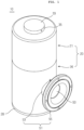
- FIG. 1 is an external perspective view of an X-ray source according to a first embodiment of the present invention
- FIG. 2 is a longitudinal cross-sectional view of FIG. 1
- FIGS. 3 , 4 and 5 are enlarged cross-sectional views of parts A, B and C of FIG. 2 .
- the X-ray source 10 may include a housing 20 which forms an external appearance.
- the housing 20 has a hollow tube shape in which vacuum is created.
- the housing 20 may include a first housing 21 with an anode electrode portion 30.
- the first housing 21 may have a hollow shape.
- the first housing 21 may be made of an insulating material.
- the first housing 21 may be made of ceramic material.
- An inner surface 21a of the first housing 21 may have a skirt shape.
- the skirt shape may have a larger inner diameter, as it descends from top to bottom, that is, moves from the anode electrode portion 30 to a cathode electrode portion 40, which will be described later.
- the first housing 21 may include a sleeve 22.
- the sleeve 22 may be formed to extend downward from the lower end of the first housing 21 facing the cathode electrode portion 40 toward the cathode electrode portion 40 through the inside of a cylindrical tube 27. Therefore, the sleeve 22 may cover a joint portion 25 of joining the lower end of the first housing 21 and the upper end of the cylindrical tube 27.
- the sleeve 22 may be integrated with the first housing 21.
- the inner surface 22a of the sleeve 22 may have a rib shape extending downward from the inner surface 21a of the first housing 21. Such a rib shape may secure the maximum insulation distance.
- the outer surface 22b of the sleeve 22 may be spaced apart from the cylindrical tube 27.
- An inclined surface 22c may be formed outside the lower end of the sleeve 22.
- the inclined surface 22c may have a funnel or dish shape whose distance from the inner surface of the cylindrical tube 27 gradually narrows as it approaches the first housing 21. Such a funnel or dish shape may smoothly introduce electric charges remaining in the internal space of the housing 20 to the second housing 26 that is on the metal side.
- the housing 20 may include a second housing 26 with the cathode electrode portion 40.
- the second housing 26 may be made of metal material.
- the second housing 26 may be grounded.
- the second housing 26 may include a cylindrical tube 27 that is made of metal.
- the upper end of the cylindrical tube 27 may be joined to the lower end of the first housing 21.
- the joining may be brazing welding, for example.
- the second housing 26 may include a bottom plate 28 that is made of metal.
- the bottom plate 28 may be a hollow plate that is donut-shaped.
- a through hole 28a may be formed in the center of the bottom plate 28.
- the edge of the bottom plate 28 may be joined to the lower end of the cylindrical tube 27. The joining may be brazing welding, for example.
- the average thickness T of the first housing 21 may be formed to be much thicker than the thickness t of the second housing 26. This is to prevent the insulation of the ceramic material of the first housing 21 from being destroyed due to the high voltage applied to the anode electrode portion 30.
- the X-ray source 10 may include an anode electrode portion 30 provided at one end of the first housing 21.
- the anode electrode portion 30 may include an anode electrode 31 disposed at the center of the inner surface of the first housing 21.
- the anode electrode 31 may be made of metal.
- the anode electrode portion 30 may include a support bundle 33 disposed outside the top of the first housing 21.
- the support bundle 33 may be made of metal.
- the support bundle 33 may be formed integrally with the top of the anode electrode 31.
- the diameter of the support bundle 33 may be larger than the diameter of the anode electrode 31 and smaller than the minimum inner diameter of the first housing 21.
- the support bundle 33 may include a support 35 made of metal.
- the support 35 may be formed on the outer peripheral surface of the support bundle 33.
- the support 35 may have an L-shaped bridge structure.
- the support 35 may include a horizontal support 35a.
- the horizontal support 35a may protrude horizontally outward from the outer peripheral surface of the support bundle 33.
- the support 35 may include a vertical support 35b.
- the vertical support 35b may protrude downward from the horizontal support 35a.
- the lower end of the vertical support 35b may be joined to the upper end of the first housing 21.
- a space 36 may be formed between the vertical support 35b and the outer peripheral surface of the support bundle 33. The support 35 and the space 36 may allow the anode electrode portion 30 to be stably fixed to the first housing 21, despite the difference in thermal expansion coefficient between dissimilar materials of the anode electrode portion 30 made of metal and the first housing 21 made of ceramic.
- the anode electrode portion 30 may include a target installation bundle 37 made of metal.
- the target installation bundle 37 may be formed integrally with the lower end of the anode electrode 31.
- the lower surface 37a of the target installation bundle 37 is inclined diagonally toward the window 50.
- the target 39 may be bonded to the lower surface 37a of the target installation bundle 37.
- the target 39 may emit X-rays to the window 50 by hitting accelerated electrons.
- the target 39 may be made of tungsten (w), copper (Cu), molybdenum (Mo), cobalt (Co), chromium (Cr), iron (Fe), silver (Ag), tantalum (Ta), yttrium (Y), and the like.
- tungsten (w) which has a high melting point and excellent X-ray emission efficiency, may be used as the target 39.
- the X-ray source 10 may include a cathode electrode portion 40.
- the cathode electrode portion 40 may be disposed in the through hole 28a of the bottom plate 28 of the second housing 26 to be spaced apart from the through hole 28a. As a result, the cathode electrode portion 40 may be electrically insulated from the second housing 26 made of metal.
- the cathode electrode portion 40 may include a cathode electrode 41.
- the cathode electrode 41 may be disposed outside the bottom plate 28 of the second housing 26.
- the cathode electrode 41 may have a convex shape.
- the cathode electrode 41 may include a cathode body 41a made of metal.
- a nanoscale emitter (not shown), such as CNTs (Carbon Nanotubes) and a metal nanotips may be disposed on the surface of the cathode body 41a.
- the cathode electrode 41 may include a cathode flange 41b made of metal.
- the cathode flange 41b may be formed integrally with the lower side of the cathode body 41a.
- the cathode electrode portion 40 may include a gate electrode 42.
- the gate electrode 42 may be provided to be spaced apart from the upper surface of the cathode body 41a. As a result, the gate electrode 42 is electrically insulated from the cathode electrode 41.
- the gate electrode 42 may be mesh-shaped.
- the gate electrode 42 may include a focus portion 43.
- the focus portion 43 may include a focus tube 43a.
- the gate electrode 42 may be bonded to the lower end of the focus tube 43a.
- the focus tube 43a may allow electrons emitted from the emitter and passing through the gate electrode 42 to be focused.
- the focus portion 43 may include a focus flange 43b.
- the focus flange 43b may be formed on the lower side of the focus tube 43a.
- a first step 43b' may be formed on the upper surface of the focus flange 43b.
- the first step 43b' may be formed to be concave downward.
- a second step 43b" may be formed on the lower surface of the focus flange 43b.
- the second step 43b" may be formed to be concave upward.
- the cathode electrode portion 40 may include a focus electrode 44.
- the focus electrode 44 may perform secondary focusing on the electrons focused in the focus portion 43.
- the focus electrode 44 may include a focus electrode hollow plate 44a.
- the inner diameter of the focus electrode hollow plate 44a may be the same as or slightly larger than that of the focus tube 43a.
- the focus electrode 44 may include a focus electrode side wall 44b.
- the focus electrode side wall 44b may extend downward from the lower edge of the focus electrode hollow plate 44a.
- the inner diameter of the focus electrode side wall 44b may be approximately the same as the outer diameter of the focus flange 43b.
- the cathode electrode portion 40 may include a first insulating spacer 45 in a tube shape.
- the first insulating spacer 45 may be provided between the cathode electrode 41 and the focus portion 43. That is, the first insulating spacer 45 may be provided between the cathode flange 41b and the second step 43b".
- the first insulating spacer 45 may separate the cathode electrode 41 and the gate electrode 42 from each other to cause them to be electrically insulated.
- the cathode electrode portion 40 may include a second insulating spacer 46 in a tube shape.
- the second insulating spacer 46 may be provided between the focus electrode 44 and the bottom plate 28 of the second housing 26 and between the focus electrode 44 and the focus portion 43. That is, the bottom of the second insulating spacer 46 is placed on the first step 43b' and the step 28b of the bottom plate 28, such that the upper surface of the second insulating spacer 46 may support the focus electrode side wall 44b.
- the second insulating spacer 46 may separate the focus portion 43 and the focus electrode 44 of the gate electrode 42 while simultaneously fixing the cathode electrode portion 40 to the second housing 26. As a result, the gate electrode 42 and the focus electrode 44 may be electrically insulated from each other.
- the cathode electrode portion 40 may be joined to these components to form an assembly.
- the cathode electrode portion 40 of such an assembly structure may be joined to the second housing 26 by pillar-welding the second insulating spacer 46 and the step 28b of the bottom plate 28.
- the X-ray source 10 may include a window 50.
- the window 50 may be provided inside the flange portion 51 provided on one side of the cylindrical tube 27 of the second housing 26 facing the target 39.
- the flange portion 51 may include a horizontal pipe 53.
- the horizontal pipe 53 may be provided on one outer surface of the cylindrical tube 27.
- the flange portion 51 may include a flange 55.
- the flange 55 may be provided at the end of the horizontal pipe 53.
- the window 50 may be provided at the interface between the horizontal pipe 53 and the flange 55.
- This flange portion 51 may not only allow the window 50 to be provided, but also provide convenience in connectivity and alignment with other devices.
- a cathode voltage may be applied to the cathode electrode 41, an anode voltage may be applied to the anode electrode portion 30, a gate voltage may be applied to the gate electrode 42, and a focus voltage may be applied to the focus electrode 44.
- the gate voltage applied to the gate electrode 42 When electrons are emitted from the emitter by the gate voltage applied to the gate electrode 42, due to the high potential difference between the cathode voltage and anode voltage that are applied to the cathode electrode 41 and the anode electrode portion 30, respectively, the electrons pass through the mesh of the gate electrode 42, accelerate toward the anode electrode portion 30, and then collide with the target 39, thereby generating X-rays. The generated X-rays pass through the window 50 to be emitted to the outside. In this process, the focus electrode 44 focuses the electrons passing through the mesh of the gate electrode 42 and moving toward the anode electrode portion 30 onto the target 39.
- the distance between the target 39 and the cathode electrode 41 may be fixed to form an electric field.
- the X-ray source 10 is configured in a so-called single power supply manner in which a cathode voltage applied to the cathode electrode represents a ground potential and an anode voltage applied to the anode electrode portion 30 represents a positive potential.
- a high voltage of a very high potential is applied to the anode electrode portion 30.
- the anode voltage may be above +120kV, for example. Therefore, the insulation of the first housing 21 is strengthened by increasing the length of the anode electrode 31 and the first housing 21, and the cathode electrode 41 is placed outside the lower end of the second housing 20 by adjusting the height of the second insulating spacer 46, thereby maintaining the distance between the target 39 and the cathode electrode 41.
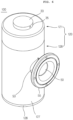
- FIG. 6 is an external perspective view of the X-ray source 100 according to a second modification of the preferred embodiment of the present invention
- FIG. 7 is a longitudinal cross-sectional view of FIG. 6
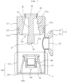
- FIG. 8 is an enlarged cross-sectional view of a part D of FIG. 7 .
- the X-ray source 100 may be configured in a dual power supply manner in which the anode voltage and cathode voltage represent positive and negative potentials, respectively.
- the anode voltage may be +60kV
- the cathode voltage may be -60kV.
- the X-ray source 100 according to the second modification has almost the same structure as the X-ray source 10 according to the first modification, they are different in that since the anode voltage is relatively low, the dielectric strength required for the first housing 21 is relatively small. Therefore, the length of the first housing is relatively short, and the cathode electrode 41 is disposed inside the second housing 126, so that the distance between the target 39 and the cathode electrode 41 may be maintained. To this end, a third insulating spacer 147 of tube shape may be added inside the second housing 126.
- the X-ray source 100 may include a housing 120 that forms an external appearance.
- the housing 120 may include a first housing 121 with an anode electrode portion 130 and a second housing 126 with a cathode electrode portion 140.
- the first housing 121 may be made of an insulating material, for example, a ceramic material, and the second housing 126 may be made of a metal material. Compared with the first modification, the first housing 121 may have a relatively short length (height).
- a sleeve 122 may be formed to extend downward the inside of the second housing 126 in the lower end of the first housing 121.
- the sleeve 122 may be made of the same material as the first housing 121.
- the inner surface 121a of the first housing 121 and the inner surface 122a of the sleeve 122 may have a skirt shape in which inner diameter increases as it moves downward.
- the outer surface 122b of the sleeve 122 may be spaced apart from the cylindrical tube 127 of the second housing 126.
- An inclined surface 122c may be formed outside the lower end of the sleeve 122.
- the inclined surface 122c may have a funnel or dish shape that gradually narrows with the inner surface of the cylindrical tube 127 as it moves toward the first housing 121.
- the second housing 126 may include a cylindrical tube 127 and a bottom plate 128.
- a through hole 128a may be formed in the center of the bottom plate 128.
- the X-ray source 100 may include an anode electrode portion 130.
- the anode electrode portion 130 may be disposed at the center of the inner surfaces of the first housing 121 and the sleeve 122.
- the anode electrode portion 130 may include an anode electrode 131, and a support bundle 33 and a target installation bundle 37 formed at the upper end and the lower end of the anode electrode 131, respectively.
- the anode electrode 131 may be covered with the first housing 121 and the sleeve 122.
- the anode electrode 131 of the dual power supply may be relatively shorter than the length (height) of the anode electrode 31 of the single power supply.
- a support 35 may be included on the outer peripheral surface of the support bundle 33.
- the support 35 may be L-shaped and include a horizontal support 35a and a vertical support 35b.
- a space 36 may be formed to allow thermal expansion between the vertical support 35b and the outer peripheral surface of the support bundle 33.
- the lower surface 37a of the target installation bundle 37 is an inclined surface to face toward the window 50, in which the target 39 may be bonded to this inclined surface.
- the X-ray source 100 may include a cathode electrode portion 140.
- the cathode electrode portion 140 may be disposed inside the second housing 126.
- the cathode electrode portion 140 may include a cathode electrode 41.
- the cathode electrode 41 may be disposed inside the housing 20.
- the cathode electrode 41 has a convex shape and may include a cathode body 41a and a cathode flange 41b.
- An emitter (not shown) may be disposed on the upper surface of the cathode body 41a.
- the cathode electrode portion 140 may include a gate electrode 42 provided on the upper surface of the cathode body 41a.
- the gate electrode 42 may have a mesh shape.
- the cathode electrode portion 140 may include a focus portion 43.
- the focus portion 43 may include a focus tube 43a and a focus flange 43b.
- the gate electrode 42 may be bonded to the lower end of the focus tube 43a.
- a first step 43b' may be formed to be downward-concave on the upper surface of the focus flange 43b.
- a second step 43b" may be formed to be upward-concave on the lower surface of the focus flange 43b.
- the cathode electrode portion 140 may include a focus electrode 144.
- the focus electrode 144 may include a focus electrode hollow plate 144a.
- An inner diameter of the focus electrode hollow plate 144a may be the same as or slightly larger than that of the focus tube 43a.
- the focus electrode 144 may include a focus electrode side wall 144b.
- the focus electrode side wall 144b may extend downward from the lower surface of the focus electrode hollow plate 144a.
- the inner diameter of the focus electrode side wall 144b may be larger than the outer diameter of the focus tube 43a.
- the focus electrode side wall 144b may be inserted into the outer peripheral surface of the focus tube 43a.
- An upwardly concave step 144b' may be formed in the lower end of the focus electrode side wall 144b.
- the focus electrode 144 may include a support flange 144c.
- the support flange 144c may protrude outward from the outer peripheral surface of the focus electrode hollow plate 144a.
- a locking protrusion 144c' may be formed at the end of the support flange 144c.
- the locking protrusion 144c' may protrude downward from the end of the support flange 144c.
- the cathode electrode portion 140 may include a first insulating spacer 45.
- the first insulating spacer 45 may be provided between the cathode electrode 41 and the focus portion 43. That is, the first insulating spacer 45 may be provided between the cathode flange 41b and the second step 43b".
- the first insulating spacer 45 separates the cathode electrode 41 and the gate electrode 42 to cause them to be electrically insulated from each other.
- the cathode electrode portion 140 may include a second insulating spacer 146.
- the second insulating spacer 146 may be provided between the focus electrode 144 and the focus portion 43. That is, the bottom of the second insulating spacer 146 may be provided between the first step 43b' and the step 144b'.
- the second insulating spacer 146 separates the focus portion 43 and the focus electrode 144 to cause them to be electrically insulated from each other.
- the X-ray source 100 may include a third insulating spacer 147.
- the third insulating spacer 147 may be provided between the focus electrode 144 and the bottom plate 128. That is, the third insulating spacer 147 may be provided to extend between the locking protrusion 144c' and the step 128b of the bottom plate 128.
- the third insulating spacer 147 may insulate the cathode electrode 41 from the second housing 126 while simultaneously fixing the cathode electrode portion 140 to the second housing 126.
- the third insulating spacer 147 may have a skirt shape in which diameter increases as it moves from the top to the bottom. Accordingly, the third insulating spacer 147 may introduce residual charges inside the housing into the second housing 127 made of metal.
- the cathode electrode portion 140 may be joined to these components to form an assembly.
- the cathode electrode portion 140 of such an assembly structure may be configured so that the lower end of the third insulating spacer 147 is joined into the step 128b of the bottom plate 128.
- the X-ray source 100 may include a window 50.
- the window 50 may be provided on the flange portion 51.
- the flange portion 51 may include a horizontal pipe 53 and a flange 55.
- the window 50 may be provided at the interface between the horizontal pipe 53 and the flange 55.
- the distance between the target 39 and the cathode electrode 41 may be fixed to form an electric field.
- the cathode electrode 41 is placed inside the housing 120, the distance between the target 39 and the cathode electrode 41 may be maintained constant, by reducing the length of the anode electrode 131 and the first housing 121 and increasing the length (or height) of the third insulating spacer 147.
- the first housing 121 and the anode electrode 131 of the X-ray source 100 of FIG. 7 may be formed to be shorter in length than the first housing 21 and the anode electrode 31 of the X-ray source 10 of FIG. 2 , but the second housing 126 of the X-ray source 100 of FIG. 7 may be formed to be longer in length than the second housing 26 of the second X-ray source 10 of FIG. 2 .
Landscapes
- X-Ray Techniques (AREA)
Applications Claiming Priority (2)
| Application Number | Priority Date | Filing Date | Title |
|---|---|---|---|
| KR1020210150643A KR102640904B1 (ko) | 2021-11-04 | 2021-11-04 | 엑스레이 소스 |
| PCT/KR2022/017188 WO2023080693A1 (ko) | 2021-11-04 | 2022-11-04 | 엑스레이 소스 |
Publications (2)
| Publication Number | Publication Date |
|---|---|
| EP4428895A1 true EP4428895A1 (de) | 2024-09-11 |
| EP4428895A4 EP4428895A4 (de) | 2025-11-19 |
Family
ID=86241889
Family Applications (1)
| Application Number | Title | Priority Date | Filing Date |
|---|---|---|---|
| EP22890424.9A Pending EP4428895A4 (de) | 2021-11-04 | 2022-11-04 | Röntgenquelle |
Country Status (6)
| Country | Link |
|---|---|
| US (1) | US20250349487A1 (de) |
| EP (1) | EP4428895A4 (de) |
| JP (1) | JP2024542012A (de) |
| KR (1) | KR102640904B1 (de) |
| CN (1) | CN118355467A (de) |
| WO (1) | WO2023080693A1 (de) |
Families Citing this family (1)
| Publication number | Priority date | Publication date | Assignee | Title |
|---|---|---|---|---|
| KR20250087308A (ko) | 2023-12-07 | 2025-06-16 | 주식회사바텍 | 전계 방출 엑스선 소스 장치 |
Family Cites Families (13)
| Publication number | Priority date | Publication date | Assignee | Title |
|---|---|---|---|---|
| EP1537594B1 (de) * | 2002-09-09 | 2006-01-25 | Comet Holding AG | Hochspannungs-vakuumröhre |
| JP2005228696A (ja) * | 2004-02-16 | 2005-08-25 | Hitachi Medical Corp | 固定陽極x線管 |
| KR100540144B1 (ko) * | 2004-06-04 | 2006-01-12 | 한국전자통신연구원 | 전계방출소자 및 이를 이용한 전계 방출 표시장치 |
| JP4786285B2 (ja) * | 2005-10-07 | 2011-10-05 | 浜松ホトニクス株式会社 | X線管 |
| CN102347186B (zh) * | 2010-07-30 | 2015-11-18 | 株式会社理学 | 工业用x射线管 |
| KR102097565B1 (ko) * | 2015-02-23 | 2020-04-06 | 주식회사 바텍 | 전계 방출 엑스선 소스 장치 |
| KR101749858B1 (ko) * | 2016-02-22 | 2017-06-21 | 경희대학교 산학협력단 | 일체형 디지털 광원장치 |
| KR101966794B1 (ko) * | 2017-07-12 | 2019-08-27 | (주)선재하이테크 | 전자 집속 개선용 엑스선관 |
| KR102005638B1 (ko) * | 2017-11-22 | 2019-07-30 | 경희대학교 산학협력단 | 바이폴라 엑스레이장치 |
| US11201031B2 (en) * | 2018-03-22 | 2021-12-14 | Varex Imaging Corporation | High voltage seals and structures having reduced electric fields |
| KR102295279B1 (ko) * | 2019-04-08 | 2021-08-30 | 주식회사 바텍 | 전계 방출 엑스선 소스 장치 및 그 제조 방법 |
| JP6792676B1 (ja) * | 2019-07-24 | 2020-11-25 | 浜松ホトニクス株式会社 | X線管 |
| KR102358246B1 (ko) | 2019-12-26 | 2022-02-07 | 주식회사 씨에이티빔텍 | 엑스레이 튜브 |
-
2021
- 2021-11-04 KR KR1020210150643A patent/KR102640904B1/ko active Active
-
2022
- 2022-11-04 CN CN202280080455.1A patent/CN118355467A/zh active Pending
- 2022-11-04 EP EP22890424.9A patent/EP4428895A4/de active Pending
- 2022-11-04 WO PCT/KR2022/017188 patent/WO2023080693A1/ko not_active Ceased
- 2022-11-04 JP JP2024525534A patent/JP2024542012A/ja active Pending
- 2022-11-04 US US18/707,841 patent/US20250349487A1/en active Pending
Also Published As
| Publication number | Publication date |
|---|---|
| JP2024542012A (ja) | 2024-11-13 |
| CN118355467A (zh) | 2024-07-16 |
| KR20230064960A (ko) | 2023-05-11 |
| EP4428895A4 (de) | 2025-11-19 |
| WO2023080693A1 (ko) | 2023-05-11 |
| KR102640904B1 (ko) | 2024-02-27 |
| US20250349487A1 (en) | 2025-11-13 |
Similar Documents
| Publication | Publication Date | Title |
|---|---|---|
| KR101966794B1 (ko) | 전자 집속 개선용 엑스선관 | |
| US9105437B2 (en) | Field emission X-ray tube and method of focusing electron beam using the same | |
| US6735282B2 (en) | X-ray tube | |
| JP5800578B2 (ja) | X線管 | |
| US10832884B2 (en) | Cylindrical X-ray tube and manufacturing method thereof | |
| JP2020526868A (ja) | 電離放射線を生成するための小型放射源、複数の放射源を備えるアセンブリ、及び放射源を製造するためのプロセス | |
| CN113272931B (zh) | X射线产生管、x射线产生装置及x射线成像装置 | |
| JP2008103326A (ja) | X線装置の電子ビームを集束し偏向するための方法及び装置 | |
| CN110379695A (zh) | X射线管 | |
| KR20070026026A (ko) | X 선관 | |
| KR101876076B1 (ko) | 디지털 광원장치 | |
| KR20160118637A (ko) | 전계 방출 엑스선 소스 장치 | |
| EP4428895A1 (de) | Röntgenquelle | |
| JP4954526B2 (ja) | X線管 | |
| KR20150114368A (ko) | 나노 구조물을 이용한 엑스선 소스 장치 및 카트리지형 엑스선 소스 장치를 이용한 엑스선 방출 장치 | |
| CN105531791A (zh) | 用于电子发射器的双管支承件 | |
| KR20220037408A (ko) | X선관 | |
| KR20160102748A (ko) | 전계 방출 엑스선 소스 장치 | |
| WO2007043412A1 (ja) | X線管及びそれを含むx線源 | |
| CN115699242B (zh) | 电场放射装置以及电场放射方法 | |
| JP2020526866A (ja) | 電離放射線を生成するための小型放射源、複数の放射源を含むアセンブリ及び放射源を製造するためのプロセス | |
| WO2018092939A1 (ko) | 전계 방출 엑스선 소스 장치 | |
| KR102477781B1 (ko) | 전자방출 소스 및 이를 포함하는 엑스레이장치 | |
| US20260051452A1 (en) | X-ray tubes | |
| JP4009082B2 (ja) | X線管 |
Legal Events
| Date | Code | Title | Description |
|---|---|---|---|
| STAA | Information on the status of an ep patent application or granted ep patent |
Free format text: STATUS: THE INTERNATIONAL PUBLICATION HAS BEEN MADE |
|
| PUAI | Public reference made under article 153(3) epc to a published international application that has entered the european phase |
Free format text: ORIGINAL CODE: 0009012 |
|
| STAA | Information on the status of an ep patent application or granted ep patent |
Free format text: STATUS: REQUEST FOR EXAMINATION WAS MADE |
|
| 17P | Request for examination filed |
Effective date: 20240424 |
|
| AK | Designated contracting states |
Kind code of ref document: A1 Designated state(s): AL AT BE BG CH CY CZ DE DK EE ES FI FR GB GR HR HU IE IS IT LI LT LU LV MC ME MK MT NL NO PL PT RO RS SE SI SK SM TR |
|
| DAV | Request for validation of the european patent (deleted) | ||
| DAX | Request for extension of the european patent (deleted) | ||
| A4 | Supplementary search report drawn up and despatched |
Effective date: 20251022 |
|
| RIC1 | Information provided on ipc code assigned before grant |
Ipc: H01J 35/16 20060101AFI20251016BHEP Ipc: H01J 35/18 20060101ALI20251016BHEP Ipc: H01J 35/06 20060101ALI20251016BHEP Ipc: H01J 35/08 20060101ALI20251016BHEP |