EP4425554A1 - Array substrate and display panel - Google Patents
Array substrate and display panel Download PDFInfo
- Publication number
- EP4425554A1 EP4425554A1 EP21810893.4A EP21810893A EP4425554A1 EP 4425554 A1 EP4425554 A1 EP 4425554A1 EP 21810893 A EP21810893 A EP 21810893A EP 4425554 A1 EP4425554 A1 EP 4425554A1
- Authority
- EP
- European Patent Office
- Prior art keywords
- line
- sharing
- pixel
- sub
- main
- Prior art date
- Legal status (The legal status is an assumption and is not a legal conclusion. Google has not performed a legal analysis and makes no representation as to the accuracy of the status listed.)
- Pending
Links
Images


Classifications
-
- G—PHYSICS
- G02—OPTICS
- G02F—OPTICAL DEVICES OR ARRANGEMENTS FOR THE CONTROL OF LIGHT BY MODIFICATION OF THE OPTICAL PROPERTIES OF THE MEDIA OF THE ELEMENTS INVOLVED THEREIN; NON-LINEAR OPTICS; FREQUENCY-CHANGING OF LIGHT; OPTICAL LOGIC ELEMENTS; OPTICAL ANALOGUE/DIGITAL CONVERTERS
- G02F1/00—Devices or arrangements for the control of the intensity, colour, phase, polarisation or direction of light arriving from an independent light source, e.g. switching, gating or modulating; Non-linear optics
- G02F1/01—Devices or arrangements for the control of the intensity, colour, phase, polarisation or direction of light arriving from an independent light source, e.g. switching, gating or modulating; Non-linear optics for the control of the intensity, phase, polarisation or colour
- G02F1/13—Devices or arrangements for the control of the intensity, colour, phase, polarisation or direction of light arriving from an independent light source, e.g. switching, gating or modulating; Non-linear optics for the control of the intensity, phase, polarisation or colour based on liquid crystals, e.g. single liquid crystal display cells
- G02F1/133—Constructional arrangements; Operation of liquid crystal cells; Circuit arrangements
- G02F1/136—Liquid crystal cells structurally associated with a semi-conducting layer or substrate, e.g. cells forming part of an integrated circuit
- G02F1/1362—Active matrix addressed cells
- G02F1/136286—Wiring, e.g. gate line, drain line
-
- G—PHYSICS
- G02—OPTICS
- G02F—OPTICAL DEVICES OR ARRANGEMENTS FOR THE CONTROL OF LIGHT BY MODIFICATION OF THE OPTICAL PROPERTIES OF THE MEDIA OF THE ELEMENTS INVOLVED THEREIN; NON-LINEAR OPTICS; FREQUENCY-CHANGING OF LIGHT; OPTICAL LOGIC ELEMENTS; OPTICAL ANALOGUE/DIGITAL CONVERTERS
- G02F1/00—Devices or arrangements for the control of the intensity, colour, phase, polarisation or direction of light arriving from an independent light source, e.g. switching, gating or modulating; Non-linear optics
- G02F1/01—Devices or arrangements for the control of the intensity, colour, phase, polarisation or direction of light arriving from an independent light source, e.g. switching, gating or modulating; Non-linear optics for the control of the intensity, phase, polarisation or colour
- G02F1/13—Devices or arrangements for the control of the intensity, colour, phase, polarisation or direction of light arriving from an independent light source, e.g. switching, gating or modulating; Non-linear optics for the control of the intensity, phase, polarisation or colour based on liquid crystals, e.g. single liquid crystal display cells
- G02F1/133—Constructional arrangements; Operation of liquid crystal cells; Circuit arrangements
- G02F1/1333—Constructional arrangements; Manufacturing methods
- G02F1/1343—Electrodes
- G02F1/134309—Electrodes characterised by their geometrical arrangement
- G02F1/134336—Matrix
-
- G—PHYSICS
- G02—OPTICS
- G02F—OPTICAL DEVICES OR ARRANGEMENTS FOR THE CONTROL OF LIGHT BY MODIFICATION OF THE OPTICAL PROPERTIES OF THE MEDIA OF THE ELEMENTS INVOLVED THEREIN; NON-LINEAR OPTICS; FREQUENCY-CHANGING OF LIGHT; OPTICAL LOGIC ELEMENTS; OPTICAL ANALOGUE/DIGITAL CONVERTERS
- G02F1/00—Devices or arrangements for the control of the intensity, colour, phase, polarisation or direction of light arriving from an independent light source, e.g. switching, gating or modulating; Non-linear optics
- G02F1/01—Devices or arrangements for the control of the intensity, colour, phase, polarisation or direction of light arriving from an independent light source, e.g. switching, gating or modulating; Non-linear optics for the control of the intensity, phase, polarisation or colour
- G02F1/13—Devices or arrangements for the control of the intensity, colour, phase, polarisation or direction of light arriving from an independent light source, e.g. switching, gating or modulating; Non-linear optics for the control of the intensity, phase, polarisation or colour based on liquid crystals, e.g. single liquid crystal display cells
- G02F1/133—Constructional arrangements; Operation of liquid crystal cells; Circuit arrangements
- G02F1/136—Liquid crystal cells structurally associated with a semi-conducting layer or substrate, e.g. cells forming part of an integrated circuit
- G02F1/1362—Active matrix addressed cells
- G02F1/136218—Shield electrodes
-
- G—PHYSICS
- G02—OPTICS
- G02F—OPTICAL DEVICES OR ARRANGEMENTS FOR THE CONTROL OF LIGHT BY MODIFICATION OF THE OPTICAL PROPERTIES OF THE MEDIA OF THE ELEMENTS INVOLVED THEREIN; NON-LINEAR OPTICS; FREQUENCY-CHANGING OF LIGHT; OPTICAL LOGIC ELEMENTS; OPTICAL ANALOGUE/DIGITAL CONVERTERS
- G02F1/00—Devices or arrangements for the control of the intensity, colour, phase, polarisation or direction of light arriving from an independent light source, e.g. switching, gating or modulating; Non-linear optics
- G02F1/01—Devices or arrangements for the control of the intensity, colour, phase, polarisation or direction of light arriving from an independent light source, e.g. switching, gating or modulating; Non-linear optics for the control of the intensity, phase, polarisation or colour
- G02F1/13—Devices or arrangements for the control of the intensity, colour, phase, polarisation or direction of light arriving from an independent light source, e.g. switching, gating or modulating; Non-linear optics for the control of the intensity, phase, polarisation or colour based on liquid crystals, e.g. single liquid crystal display cells
- G02F1/133—Constructional arrangements; Operation of liquid crystal cells; Circuit arrangements
- G02F1/136—Liquid crystal cells structurally associated with a semi-conducting layer or substrate, e.g. cells forming part of an integrated circuit
- G02F1/1362—Active matrix addressed cells
- G02F1/13624—Active matrix addressed cells having more than one switching element per pixel
-
- G—PHYSICS
- G02—OPTICS
- G02F—OPTICAL DEVICES OR ARRANGEMENTS FOR THE CONTROL OF LIGHT BY MODIFICATION OF THE OPTICAL PROPERTIES OF THE MEDIA OF THE ELEMENTS INVOLVED THEREIN; NON-LINEAR OPTICS; FREQUENCY-CHANGING OF LIGHT; OPTICAL LOGIC ELEMENTS; OPTICAL ANALOGUE/DIGITAL CONVERTERS
- G02F1/00—Devices or arrangements for the control of the intensity, colour, phase, polarisation or direction of light arriving from an independent light source, e.g. switching, gating or modulating; Non-linear optics
- G02F1/01—Devices or arrangements for the control of the intensity, colour, phase, polarisation or direction of light arriving from an independent light source, e.g. switching, gating or modulating; Non-linear optics for the control of the intensity, phase, polarisation or colour
- G02F1/13—Devices or arrangements for the control of the intensity, colour, phase, polarisation or direction of light arriving from an independent light source, e.g. switching, gating or modulating; Non-linear optics for the control of the intensity, phase, polarisation or colour based on liquid crystals, e.g. single liquid crystal display cells
- G02F1/133—Constructional arrangements; Operation of liquid crystal cells; Circuit arrangements
- G02F1/136—Liquid crystal cells structurally associated with a semi-conducting layer or substrate, e.g. cells forming part of an integrated circuit
- G02F1/1362—Active matrix addressed cells
- G02F1/1368—Active matrix addressed cells in which the switching element is a three-electrode device
-
- G—PHYSICS
- G02—OPTICS
- G02F—OPTICAL DEVICES OR ARRANGEMENTS FOR THE CONTROL OF LIGHT BY MODIFICATION OF THE OPTICAL PROPERTIES OF THE MEDIA OF THE ELEMENTS INVOLVED THEREIN; NON-LINEAR OPTICS; FREQUENCY-CHANGING OF LIGHT; OPTICAL LOGIC ELEMENTS; OPTICAL ANALOGUE/DIGITAL CONVERTERS
- G02F1/00—Devices or arrangements for the control of the intensity, colour, phase, polarisation or direction of light arriving from an independent light source, e.g. switching, gating or modulating; Non-linear optics
- G02F1/01—Devices or arrangements for the control of the intensity, colour, phase, polarisation or direction of light arriving from an independent light source, e.g. switching, gating or modulating; Non-linear optics for the control of the intensity, phase, polarisation or colour
- G02F1/13—Devices or arrangements for the control of the intensity, colour, phase, polarisation or direction of light arriving from an independent light source, e.g. switching, gating or modulating; Non-linear optics for the control of the intensity, phase, polarisation or colour based on liquid crystals, e.g. single liquid crystal display cells
- G02F1/133—Constructional arrangements; Operation of liquid crystal cells; Circuit arrangements
- G02F1/1333—Constructional arrangements; Manufacturing methods
- G02F1/1343—Electrodes
- G02F1/134309—Electrodes characterised by their geometrical arrangement
- G02F1/134345—Subdivided pixels, e.g. for grey scale or redundancy
-
- G—PHYSICS
- G02—OPTICS
- G02F—OPTICAL DEVICES OR ARRANGEMENTS FOR THE CONTROL OF LIGHT BY MODIFICATION OF THE OPTICAL PROPERTIES OF THE MEDIA OF THE ELEMENTS INVOLVED THEREIN; NON-LINEAR OPTICS; FREQUENCY-CHANGING OF LIGHT; OPTICAL LOGIC ELEMENTS; OPTICAL ANALOGUE/DIGITAL CONVERTERS
- G02F1/00—Devices or arrangements for the control of the intensity, colour, phase, polarisation or direction of light arriving from an independent light source, e.g. switching, gating or modulating; Non-linear optics
- G02F1/01—Devices or arrangements for the control of the intensity, colour, phase, polarisation or direction of light arriving from an independent light source, e.g. switching, gating or modulating; Non-linear optics for the control of the intensity, phase, polarisation or colour
- G02F1/13—Devices or arrangements for the control of the intensity, colour, phase, polarisation or direction of light arriving from an independent light source, e.g. switching, gating or modulating; Non-linear optics for the control of the intensity, phase, polarisation or colour based on liquid crystals, e.g. single liquid crystal display cells
- G02F1/133—Constructional arrangements; Operation of liquid crystal cells; Circuit arrangements
- G02F1/1333—Constructional arrangements; Manufacturing methods
- G02F1/1343—Electrodes
- G02F1/134309—Electrodes characterised by their geometrical arrangement
- G02F1/134363—Electrodes characterised by their geometrical arrangement for applying an electric field parallel to the substrate, i.e. in-plane switching [IPS]
Definitions
- the present disclosure relates to a field of display technology, in particular to an array substrate and a display panel.
- an electric field of a data line may cause surrounding liquid crystals to flip, resulting in light leakage.
- a distance between the data line and a pixel electrode is relatively short, thus a capacitive coupling of the data line to the pixel electrode may cause adverse effects such as crosstalk.
- a data line BM less (DBS) technique may be used to remove the black matrix above the data line, and a DBS electrode may be provided above the data line, so that a potential of the DBS electrode is same as a potential of a common electrode on a color film substrate, so that corresponding liquid crystal molecules above the data line remain in an undeflected state at all times, thereby performing light shielding.
- DBS data line BM less
- a common electrode line 200' may be used on a side of a data line 100' to shield a lateral electric field of the data line 100', so as to reduce an influence of the data line to a pixel electrode.
- a com a common electrode line 200'
- a sharing electrode line 300' shared bar of a sharing thin film transistor penetrates a main pixel region and a sub-pixel region vertically, thereby reducing a light transmission area of the pixel unit and reducing the aperture ratio and a transmittance of the pixel unit.
- the present disclosure aims to provide an array substrate and a display panel, which can solve problems in the prior art that using a common electrode line to shield a lateral electric field of a data line may cause a low aperture ratio of a display panel.
- an array substrate comprising a substrate and a plurality of pixel units arranged on the substrate in array; each of the pixel units comprises: a data line disposed on the substrate; a scan line disposed on the substrate and intersecting with the data line; and a first sharing line disposed between the substrate and the data line and parallel to the data line.
- the first sharing line has a first central axis parallel to the data line; the data line has a second central axis parallel to the first sharing line; and the first central axis and the second central axis coincide with each other.
- a width of the first sharing line and a width of the data line are uniformly set, and the width of the first sharing line is greater than or equal to the width of the data line.
- each of the pixel units is divided into a main pixel region and a sub-pixel region, and the scan line is disposed between the main pixel region and the sub-pixel region; each of the pixel units further comprises: a second sharing line parallel to the scan line and disposed between the scan line and the sub-pixel region; and a first common line parallel to the scan line and disposed between the scan line and the main pixel region; wherein one end of the first sharing line is electrically connected to the second sharing line, and another end of the first sharing line extends along the first axis from the sub-pixel region of one of the pixel units to the main pixel region of an adjacent pixel unit.
- the scan line, the second sharing line, the first common line, and the first sharing line are disposed in a same layer.
- each of the pixel units further comprises: a main pixel electrode disposed in the main pixel region, wherein the main pixel electrode comprises a first main electrode parallel to the data line; a sub-pixel electrode disposed in the sub-pixel region, wherein the sub-pixel electrode comprises a second main electrode parallel to the data line; a main pixel thin film transistor, wherein a gate of the main thin film transistor is electrically connected to the scan line, a source of the main thin film transistor is electrically connected to the data line, and a drain of the main thin film transistor is electrically connected to the main pixel electrode; a sub-pixel thin film transistor, wherein a gate of the sub-pixel thin film transistor is electrically connected to the scan line, a source of the sub-pixel thin film transistor is electrically connected to the data line, and a drain of the sub-pixel thin film transistor is electrically connected to the sub-pixel electrode; and a sharing thin film transistor, wherein a gate of the sharing thin film transistor is electrically connected to the scan line, a source of the data line
- each of the pixel units further comprises: a third sharing line, wherein one end of the third sharing line is electrically connected to the second sharing line and another end of the third sharing line extends along the first axis from the sub-pixel region of one of the pixel units to the main pixel region of an adjacent pixel unit.
- each of the pixel units further comprises: a second common line, one end of the second common line is electrically connected to the first common line and another end of the second common line extends along the first axis from the main pixel region of one of the pixel units to the sub-pixel region of an adjacent pixel unit.
- the third sharing line in the main pixel region is disposed corresponding to the first main electrode, and the third sharing line in the sub-pixel region is disposed corresponding to the second main electrode.
- the second common line in the main pixel region is disposed corresponding to the first main electrode, and the second common line in the sub-pixel region is disposed corresponding to the second main electrode.
- the present disclosure provides a display panel, comprising an array substrate according to the present disclosure, a color film substrate disposed corresponding to the array substrate, and a liquid crystal layer disposed between the array substrate and the color film substrate.
- the first sharing line is correspondingly disposed under the data line, an electric field of the data line is shielded through the first sharing line, coupling between the data line and the first common line is relieved through the first sharing line, a crosstalk caused to the data line due to fluctuation of the first common line is reduced, and a problem in the prior art that using a common electrode line to shield a lateral electric field of the data line causes a low aperture ratio of a display panel is prevented.
- the first central axis of the first sharing line and the second central axis of the data line coincide with each other, thereby preventing a situation in the prior art that the first sharing line penetrates the main pixel region and the sub-pixel region vertically, and thereby improving an aperture ratio and transmittance of the pixel units.
- the display panel comprises an array substrate 100, a color film substrate disposed corresponding to the array substrate 100, and a liquid crystal layer disposed between the array substrate 100 and the color film substrate.
- the array substrate 100 comprises a substrate 101 and a plurality of pixel units 102 arranged on the substrate 101 in array.
- the substrate 101 is made of one or more of glass, polyimide, polycarbonate, polyethylene terephthalate, and polyethylene naphthalate. Therefore, the substrate 101 has better impact resistance and can effectively protect the display panel.
- each of the pixel units 102 is divided into a main pixel region 1021 and a sub-pixel region 1022.
- Each of the pixel units 102 comprises a data line 1, a scan line 2, a first sharing line 3, a second sharing line 4, a first common line 5, a main pixel electrode 6, a sub-pixel electrode 7, a main pixel thin film transistor 8, a sub-pixel thin film transistor 9, a sharing thin film transistor 10, and a third sharing line 11.
- the data line 1 is disposed on the substrate 101.
- a material of the data line 1 is metal.
- materials of the data line 1 may also be other conductive materials. For example, alloys, nitrides of metallic materials, oxides of metallic materials, nitrogen oxides of metallic materials, stacked layers of metallic materials and other conductive materials, or other suitable materials.
- the scan line 2 is disposed between the main pixel region 1021 and the sub-pixel region 1022, and intersects with the data line 1. That is, an extension direction of the data line 1 is not parallel to an extension direction of the scan line 2. In this embodiment, the extension direction of the data line 1 and the extension direction of the scan line 2 are perpendicular to each other.
- a material of the scan line 2 is metal. In other embodiments, materials of the scan line 2 may also be other conductive materials. For example, alloys, nitrides of metallic materials, oxides of metallic materials, nitrogen oxides of metallic materials, stacked layers of metallic materials and other conductive materials, or other suitable materials.
- the first sharing line 3 is disposed between the substrate 101 and the data line 1, and parallel to the data line 1.
- a material of the first sharing line 3 is metal.
- materials of the first sharing line 3 may also be other conductive materials. For example, alloys, nitrides of metallic materials, oxides of metallic materials, nitrogen oxides of metallic materials, stacked layers of metallic materials and other conductive materials, or other suitable materials.
- An electric field of the data line 1 is shielded by the first sharing line 3, and a coupling effect between the data line 1 and the first common line 5 is relieved by the first sharing line 3, thereby reducing crosstalk to the data line 1 by fluctuation of the first common line 5.
- the first sharing line 3 has a first central axis 12 parallel to the data line 1, and the first central axis 12 is a symmetrical axis.
- the data line 1 has a second central axis 13 parallel to the first sharing line 3, and the second central axis 13 is a symmetrical axis.
- the first central axis 12 and the second central axis 13 coincide with each other.
- the first central axis 12 of the first sharing line 3 coincides with the second central axis 13 of the data line 1 to prevent a situation in the prior art that the first sharing line 3 penetrates the main pixel region 1021 and the sub-pixel region 1022 vertically, thereby increasing an aperture ratio and transmittance of the array substrate 100.
- one end of the first sharing line 3 is electrically connected to the second sharing line 4, and another end extends along the first axis 1011 from the sub-pixel region 1022 of one of the pixel units 102 to the main pixel region 1021 of an adjacent pixel unit 102.
- a width of the first sharing line 3 is uniformly set, a width of the data line 1 is uniformly set, and the width of the first sharing line 3 is greater than or equal to the width of the data line 1.
- a difference value between the width of the first sharing line 3 and the width of the data line 1 ranges from 0 ⁇ m to 15 ⁇ m.
- the difference value between the width of the first sharing line 3 and the width of the data line 1 is relatively small, an effect of shielding the electric field of the data line 1 by the first sharing line 3 is poor.
- the difference value between the width of the first sharing line 3 and the width of the data line 1 is greater than 15 ⁇ m, the first sharing line 3 will occupy an aperture area of the array substrate 100, and the aperture ratio and transmittance of the array substrate 100 is reduced.
- an insulating layer 14 is also disposed between the first sharing line 3 and the data line 1.
- the insulating layer 14 is mainly used to prevent contact between the first sharing line 3 and the data line 1 from causing a short circuit phenomenon.
- Materials of the insulating layer 14 may be one or more of SiO 2 and SiN x .
- the second sharing line 4 parallels to the scan line 2 and disposed between the scan line 2 and the sub-pixel region 1022, and spacedly disposed from the scan line 2.
- a material of the second sharing line 4 is metal.
- materials of the second sharing line 4 may also be other conductive materials. For example, alloys, nitrides of metallic materials, oxides of metallic materials, nitrogen oxides of metallic materials, stacked layers of metallic materials and other conductive materials, or other suitable materials.
- the first common line 5 parallels to the scan line 2 and disposed between the scan line 2 and the main pixel region 1021, and spacedly disposed from the scan line 2.
- a material of the first common line 5 is metal.
- materials of the first common line 5 may also be other conductive materials. For example, alloys, nitrides of metallic materials, oxides of metallic materials, nitrogen oxides of metallic materials, stacked layers of metallic materials and other conductive materials, or other suitable materials.
- the scan line 2, the second sharing line 4, the first common line 5, and the first sharing line 3 are disposed in a same layer.
- the scan line 2, the second sharing line 4, the first common line 5, and the first sharing line 3 are made of a same material, so that the scan line 2, the second sharing line 4, the first common line 5, and the first sharing line 3 can be simultaneously prepared in one step, thereby saving processes and production costs.
- the main pixel electrode 6 is disposed in the main pixel region 1021.
- the main pixel electrode 6 comprises a first main electrode 61 parallel to the data line 1.
- the sub-pixel electrode 7 is disposed in the sub-pixel region 1022.
- the sub-pixel electrode 7 comprises a second main electrode 71 parallel to the data line 1.
- a gate of the main pixel thin film transistor 8 (i.e., T1 in FIG. 4 ) is electrically connected to the scan line 2 (i.e., Gate in FIG. 4 ), a source of the main pixel thin film transistor 8 (i.e., T1 in FIG. 4 ) is electrically connected to the data line 1 (i.e., Data in FIG. 4 ), and a drain of the main pixel thin film transistor 8 (i.e., T1 in FIG. 4 ) is electrically connected to the main pixel electrode 6.
- a gate of the sub-pixel thin film transistor 9 (i.e., T2 in FIG. 4 ) is electrically connected to the scan line 2 (i.e., Gate in FIG. 4 ), a source of the sub-pixel thin film transistor 9 (i.e., T2 in FIG. 4 ) is electrically connected to the data line 1 (i.e., Data in FIG. 4 ), and a drain of the sub-pixel thin film transistor 9 (i.e., T2 in FIG. 4 ) is electrically connected to the sub-pixel electrode 7.
- a gate of the sharing thin film transistor 10 (i.e., T3 in FIG. 4 ) is electrically connected to the scan line 2 (i.e., Gate in FIG. 4 ), a source of the sharing thin film transistor 10 (i.e., T3 in FIG. 4 ) is electrically connected to the drain of the sub-pixel thin film transistor 9 (i.e., T2 in FIG. 4 ), and a drain of the sharing thin film transistor 10 (i.e., T3 in FIG. 4 ) is electrically connected to the second sharing line 4.
- the gate of the main pixel thin film transistor 8, the gate of the sub-pixel thin film transistor 9, and the gate of the sharing thin film transistor 10 are electrically connected to the same scan line 2.
- the source of the main pixel thin film transistor 8 and the source of the sub-pixel thin film transistor 9 are electrically connected to the same data line 1.
- one end of the third sharing line 11 is electrically connected to the second sharing line 4, and another end extends along the first axis 1011 from the sub-pixel region 1022 of one of the pixel units 102 to the main pixel region 1021 of an adjacent pixel unit 102.
- the third sharing line 11 in the main pixel region 1021 disposed corresponding to the first main electrode 61, and the third sharing line 11 in the sub-pixel region 1022 disposed corresponding to the second main electrode 71 Therefore, an additional occupation of the transmission area of the array substrate 100 is prevented, and the aperture ratio of the array substrate 100 is increased.
- Embodiment 2 includes most technical features of Embodiment 1.
- Embodiment 2 differs from Embodiment 1 in that the third sharing line 11 of Embodiment 1 is removed from Embodiment 2, and a second common line 15 is disposed at a position of the third sharing line 11 of Embodiment 1.
- one end of the second common line 15 is electrically connected to the first common line 5, and another end of the second common line 15 extends along the first axis 1011 from the main pixel region 1021 of one of the pixel units 102 to the sub-pixel region 1022 of an adjacent pixel unit 102.
- the second common line 15 in the main pixel region 1021 is disposed corresponding to the first main electrode 61, and the second common line 15 in the sub-pixel region 1022 corresponds to the second main electrode 71. Therefore, an additional occupation of the transmission area of the array substrate 100 is prevented, and the aperture ratio of the substrate 100 is increased.
- the electric field of the data line 1 is shielded by the first sharing line 3, and a coupling effect between the data line 1 and the first common line 5 is relieved by the first sharing line 3, thereby reducing crosstalk caused to the data line 1 by fluctuation of the first common line 5.
- the first central axis 12 of the first sharing line 3 coincides with the second central axis 13 of the data line 1 to prevent a situation in the prior art that the first sharing line 3 penetrates the main pixel region 1021 and the sub-pixel region 1022 vertically, thereby increasing the aperture ratio and the transmittance of the array substrate 100.
Landscapes
- Physics & Mathematics (AREA)
- Nonlinear Science (AREA)
- Mathematical Physics (AREA)
- Chemical & Material Sciences (AREA)
- Crystallography & Structural Chemistry (AREA)
- General Physics & Mathematics (AREA)
- Optics & Photonics (AREA)
- Engineering & Computer Science (AREA)
- Microelectronics & Electronic Packaging (AREA)
- Geometry (AREA)
- Liquid Crystal (AREA)
- Devices For Indicating Variable Information By Combining Individual Elements (AREA)
Abstract
Description
- The present disclosure relates to a field of display technology, in particular to an array substrate and a display panel.
- At present, in an array substrate of a thin film transistor liquid crystal display (TFT LCD), an electric field of a data line may cause surrounding liquid crystals to flip, resulting in light leakage. Moreover, a distance between the data line and a pixel electrode is relatively short, thus a capacitive coupling of the data line to the pixel electrode may cause adverse effects such as crosstalk.
- At present, in addition to providing a black matrix (BM) above the data line for light shielding, a data line BM less (DBS) technique may be used to remove the black matrix above the data line, and a DBS electrode may be provided above the data line, so that a potential of the DBS electrode is same as a potential of a common electrode on a color film substrate, so that corresponding liquid crystal molecules above the data line remain in an undeflected state at all times, thereby performing light shielding.
- As shown in
FIGs. 1 and2 , a common electrode line 200' (A com) may be used on a side of a data line 100' to shield a lateral electric field of the data line 100', so as to reduce an influence of the data line to a pixel electrode. However, using the common electrode line 200' to shield the lateral electric field of the date line 100' will reduce an aperture ratio of a pixel unit. Further, a sharing electrode line 300' (share bar) of a sharing thin film transistor penetrates a main pixel region and a sub-pixel region vertically, thereby reducing a light transmission area of the pixel unit and reducing the aperture ratio and a transmittance of the pixel unit. - The present disclosure aims to provide an array substrate and a display panel, which can solve problems in the prior art that using a common electrode line to shield a lateral electric field of a data line may cause a low aperture ratio of a display panel.
- To solve the above problems, the present disclosure provides an array substrate, comprising a substrate and a plurality of pixel units arranged on the substrate in array; each of the pixel units comprises: a data line disposed on the substrate; a scan line disposed on the substrate and intersecting with the data line; and a first sharing line disposed between the substrate and the data line and parallel to the data line.
- In addition, the first sharing line has a first central axis parallel to the data line; the data line has a second central axis parallel to the first sharing line; and the first central axis and the second central axis coincide with each other.
- In addition, a width of the first sharing line and a width of the data line are uniformly set, and the width of the first sharing line is greater than or equal to the width of the data line.
- In addition, each of the pixel units is divided into a main pixel region and a sub-pixel region, and the scan line is disposed between the main pixel region and the sub-pixel region; each of the pixel units further comprises: a second sharing line parallel to the scan line and disposed between the scan line and the sub-pixel region; and a first common line parallel to the scan line and disposed between the scan line and the main pixel region; wherein one end of the first sharing line is electrically connected to the second sharing line, and another end of the first sharing line extends along the first axis from the sub-pixel region of one of the pixel units to the main pixel region of an adjacent pixel unit.
- In addition, the scan line, the second sharing line, the first common line, and the first sharing line are disposed in a same layer.
- In addition, each of the pixel units further comprises: a main pixel electrode disposed in the main pixel region, wherein the main pixel electrode comprises a first main electrode parallel to the data line; a sub-pixel electrode disposed in the sub-pixel region, wherein the sub-pixel electrode comprises a second main electrode parallel to the data line; a main pixel thin film transistor, wherein a gate of the main thin film transistor is electrically connected to the scan line, a source of the main thin film transistor is electrically connected to the data line, and a drain of the main thin film transistor is electrically connected to the main pixel electrode; a sub-pixel thin film transistor, wherein a gate of the sub-pixel thin film transistor is electrically connected to the scan line, a source of the sub-pixel thin film transistor is electrically connected to the data line, and a drain of the sub-pixel thin film transistor is electrically connected to the sub-pixel electrode; and a sharing thin film transistor, wherein a gate of the sharing thin film transistor is electrically connected to the scan line, a source of the sharing thin film transistor is electrically connected to the drain of the sub-pixel thin film transistor, and a drain of the sharing thin film transistor is electrically connected to the second sharing line.
- In addition, each of the pixel units further comprises: a third sharing line, wherein one end of the third sharing line is electrically connected to the second sharing line and another end of the third sharing line extends along the first axis from the sub-pixel region of one of the pixel units to the main pixel region of an adjacent pixel unit.
- In addition, each of the pixel units further comprises: a second common line, one end of the second common line is electrically connected to the first common line and another end of the second common line extends along the first axis from the main pixel region of one of the pixel units to the sub-pixel region of an adjacent pixel unit.
- In addition, the third sharing line in the main pixel region is disposed corresponding to the first main electrode, and the third sharing line in the sub-pixel region is disposed corresponding to the second main electrode.
- In addition, the second common line in the main pixel region is disposed corresponding to the first main electrode, and the second common line in the sub-pixel region is disposed corresponding to the second main electrode.
- In order to solve the above problems, the present disclosure provides a display panel, comprising an array substrate according to the present disclosure, a color film substrate disposed corresponding to the array substrate, and a liquid crystal layer disposed between the array substrate and the color film substrate.
- In the present application, the first sharing line is correspondingly disposed under the data line, an electric field of the data line is shielded through the first sharing line, coupling between the data line and the first common line is relieved through the first sharing line, a crosstalk caused to the data line due to fluctuation of the first common line is reduced, and a problem in the prior art that using a common electrode line to shield a lateral electric field of the data line causes a low aperture ratio of a display panel is prevented. In the present disclosure, the first central axis of the first sharing line and the second central axis of the data line coincide with each other, thereby preventing a situation in the prior art that the first sharing line penetrates the main pixel region and the sub-pixel region vertically, and thereby improving an aperture ratio and transmittance of the pixel units.
- In order to more clearly explain technical solutions in embodiments of the present disclosure, the following will briefly introduce drawings required in the description of the embodiments. Obviously, the drawings in the following description are only some embodiments of the present disclosure. For those skilled in the art, without paying any creative work, other drawings can be obtained based on these drawings.
-
FIG. 1 is a schematic plan view of a pixel unit of an array substrate in the prior art. -
FIG. 2 is a cross-sectional view of A-A inFIG. 1 . -
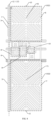
FIG. 3 is a schematic plan view of an array substrate according to Embodiment 1 of the present disclosure. -
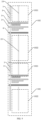
FIG. 4 is a schematic plan view of a pixel unit of the array substrate according to Embodiment 1 of the present disclosure. -
FIG. 5 is a cross-sectional view of B-B inFIG. 4 . -
FIG. 6 is a driving circuit diagram of the array substrate according to Embodiment 1 of the present disclosure. -
FIG. 7 is a schematic partial plan view of two pixel units of the array substrate according to Embodiment 1 of the present disclosure. -
FIG. 8 is a schematic plan view of a pixel unit of an array substrate according to Embodiment 2 of the present disclosure. -
FIG. 9 is a schematic partial plan view of two pixel units of the array substrate according to Embodiment 2 of the present disclosure. -
- 100, array substrate; 101, substrate;
- 102, pixel unit;
- 1021, main pixel region; 1022, sub-pixel region;
- 1, data line; 2, scan line;
- 3, first sharing line; 4, second sharing line;
- 5, first common line; 6, main pixel electrode;
- 7, sub-pixel electrode; 8, main pixel thin film transistor;
- 9, sub-pixel thin film transistor; 10, sharing thin film transistor;
- 11, third sharing line; 12, first central axis;
- 13, second central axis; 14, insulating layer;
- 15, second common line; 61, first main electrode;
- 71, second main electrode.
- The following describes preferred embodiments of the present disclosure in detail with reference to accompanying drawings of the specification, to fully introduce technical contents of the present disclosure to those skilled in the art, to exemplify that the present disclosure can be practiced, so that the technical contents disclosed by the present disclosure is clearer, and those skilled in the art can more easily understand how to implement the present disclosure. However, the present disclosure can be embodied by many different forms of embodiments, the protection scope of the present disclosure is not limited to the embodiments mentioned here, and the description of the following embodiments is not intended to limit the scope of the present disclosure.
- Directional terms mentioned in the present disclosure, such as [up], [down], [front], [back], [left], [right], [inner], [outer], [side], etc., are only directions of the attached drawings. The directional terms used in the present disclosure are used to describe and understand the present disclosure, rather than to limit the protection scope of the present disclosure.
- In the drawings, elements of a same structure are denoted by a same numeral and components of similar structure or function are denoted by similar numerals. Further, for ease of understanding and description, dimensions and thickness of each component shown in the drawings are arbitrarily shown, and the present disclosure does not limit the dimensions and thickness of each component.
- This embodiment provides a display panel. The display panel comprises an
array substrate 100, a color film substrate disposed corresponding to thearray substrate 100, and a liquid crystal layer disposed between thearray substrate 100 and the color film substrate. - As shown in
FIG. 3 , thearray substrate 100 comprises asubstrate 101 and a plurality ofpixel units 102 arranged on thesubstrate 101 in array. - The
substrate 101 is made of one or more of glass, polyimide, polycarbonate, polyethylene terephthalate, and polyethylene naphthalate. Therefore, thesubstrate 101 has better impact resistance and can effectively protect the display panel. - As shown in
FIG. 4 , each of thepixel units 102 is divided into amain pixel region 1021 and asub-pixel region 1022. Each of thepixel units 102 comprises a data line 1, a scan line 2, afirst sharing line 3, asecond sharing line 4, a firstcommon line 5, amain pixel electrode 6, asub-pixel electrode 7, a main pixelthin film transistor 8, a sub-pixelthin film transistor 9, a sharingthin film transistor 10, and athird sharing line 11. - As shown in
FIGs. 3 ,4 , and5 , the data line 1 is disposed on thesubstrate 101. In this embodiment, a material of the data line 1 is metal. In other embodiments, materials of the data line 1 may also be other conductive materials. For example, alloys, nitrides of metallic materials, oxides of metallic materials, nitrogen oxides of metallic materials, stacked layers of metallic materials and other conductive materials, or other suitable materials. - As shown in
FIGs. 3 and4 , the scan line 2 is disposed between themain pixel region 1021 and thesub-pixel region 1022, and intersects with the data line 1. That is, an extension direction of the data line 1 is not parallel to an extension direction of the scan line 2. In this embodiment, the extension direction of the data line 1 and the extension direction of the scan line 2 are perpendicular to each other. In this embodiment, a material of the scan line 2 is metal. In other embodiments, materials of the scan line 2 may also be other conductive materials. For example, alloys, nitrides of metallic materials, oxides of metallic materials, nitrogen oxides of metallic materials, stacked layers of metallic materials and other conductive materials, or other suitable materials. - As shown in
FIGs. 3 ,4 and5 , thefirst sharing line 3 is disposed between thesubstrate 101 and the data line 1, and parallel to the data line 1. In this embodiment, a material of thefirst sharing line 3 is metal. In other embodiments, materials of thefirst sharing line 3 may also be other conductive materials. For example, alloys, nitrides of metallic materials, oxides of metallic materials, nitrogen oxides of metallic materials, stacked layers of metallic materials and other conductive materials, or other suitable materials. - An electric field of the data line 1 is shielded by the
first sharing line 3, and a coupling effect between the data line 1 and the firstcommon line 5 is relieved by thefirst sharing line 3, thereby reducing crosstalk to the data line 1 by fluctuation of the firstcommon line 5. A problem in the prior art, of using a common electrode line to shield a lateral electric field of a data line, resulting in a low aperture ratio of the display panel, is prevented. - As shown in
FIGs. 3 ,4 and5 , thefirst sharing line 3 has a firstcentral axis 12 parallel to the data line 1, and the firstcentral axis 12 is a symmetrical axis. The data line 1 has a secondcentral axis 13 parallel to thefirst sharing line 3, and the secondcentral axis 13 is a symmetrical axis. The firstcentral axis 12 and the secondcentral axis 13 coincide with each other. The firstcentral axis 12 of thefirst sharing line 3 coincides with the secondcentral axis 13 of the data line 1 to prevent a situation in the prior art that thefirst sharing line 3 penetrates themain pixel region 1021 and thesub-pixel region 1022 vertically, thereby increasing an aperture ratio and transmittance of thearray substrate 100. - As shown in
FIG. 7 , one end of thefirst sharing line 3 is electrically connected to thesecond sharing line 4, and another end extends along the first axis 1011 from thesub-pixel region 1022 of one of thepixel units 102 to themain pixel region 1021 of anadjacent pixel unit 102. - As shown in
FIGs. 4 and5 , a width of thefirst sharing line 3 is uniformly set, a width of the data line 1 is uniformly set, and the width of thefirst sharing line 3 is greater than or equal to the width of the data line 1. Specifically, a difference value between the width of thefirst sharing line 3 and the width of the data line 1 ranges from 0µm to 15µm. When the difference value between the width of thefirst sharing line 3 and the width of the data line 1 is relatively small, an effect of shielding the electric field of the data line 1 by thefirst sharing line 3 is poor. When the difference value between the width of thefirst sharing line 3 and the width of the data line 1 is greater than 15µm, thefirst sharing line 3 will occupy an aperture area of thearray substrate 100, and the aperture ratio and transmittance of thearray substrate 100 is reduced. - As shown in
FIG. 5 , an insulatinglayer 14 is also disposed between thefirst sharing line 3 and the data line 1. The insulatinglayer 14 is mainly used to prevent contact between thefirst sharing line 3 and the data line 1 from causing a short circuit phenomenon. Materials of the insulatinglayer 14 may be one or more of SiO2 and SiNx. - As shown in
FIGs. 3 and4 , thesecond sharing line 4 parallels to the scan line 2 and disposed between the scan line 2 and thesub-pixel region 1022, and spacedly disposed from the scan line 2. In this embodiment, a material of thesecond sharing line 4 is metal. In other embodiments, materials of thesecond sharing line 4 may also be other conductive materials. For example, alloys, nitrides of metallic materials, oxides of metallic materials, nitrogen oxides of metallic materials, stacked layers of metallic materials and other conductive materials, or other suitable materials. - As shown in
FIGs. 3 and4 , the firstcommon line 5 parallels to the scan line 2 and disposed between the scan line 2 and themain pixel region 1021, and spacedly disposed from the scan line 2. In this embodiment, a material of the firstcommon line 5 is metal. In other embodiments, materials of the firstcommon line 5 may also be other conductive materials. For example, alloys, nitrides of metallic materials, oxides of metallic materials, nitrogen oxides of metallic materials, stacked layers of metallic materials and other conductive materials, or other suitable materials. - Wherein, the scan line 2, the
second sharing line 4, the firstcommon line 5, and thefirst sharing line 3 are disposed in a same layer. In this embodiment, the scan line 2, thesecond sharing line 4, the firstcommon line 5, and thefirst sharing line 3 are made of a same material, so that the scan line 2, thesecond sharing line 4, the firstcommon line 5, and thefirst sharing line 3 can be simultaneously prepared in one step, thereby saving processes and production costs. - As shown in
FIG. 4 , themain pixel electrode 6 is disposed in themain pixel region 1021. Themain pixel electrode 6 comprises a firstmain electrode 61 parallel to the data line 1. - As shown in
FIG. 4 , thesub-pixel electrode 7 is disposed in thesub-pixel region 1022. Thesub-pixel electrode 7 comprises a secondmain electrode 71 parallel to the data line 1. - As shown in
FIGs. 4 and6 , a gate of the main pixel thin film transistor 8 (i.e., T1 inFIG. 4 ) is electrically connected to the scan line 2 (i.e., Gate inFIG. 4 ), a source of the main pixel thin film transistor 8 (i.e., T1 inFIG. 4 ) is electrically connected to the data line 1 (i.e., Data inFIG. 4 ), and a drain of the main pixel thin film transistor 8 (i.e., T1 inFIG. 4 ) is electrically connected to themain pixel electrode 6. - As shown in
FIGs. 4 and6 , a gate of the sub-pixel thin film transistor 9 (i.e., T2 inFIG. 4 ) is electrically connected to the scan line 2 (i.e., Gate inFIG. 4 ), a source of the sub-pixel thin film transistor 9 (i.e., T2 inFIG. 4 ) is electrically connected to the data line 1 (i.e., Data inFIG. 4 ), and a drain of the sub-pixel thin film transistor 9 (i.e., T2 inFIG. 4 ) is electrically connected to thesub-pixel electrode 7. - As shown in
FIGs. 4 and6 , a gate of the sharing thin film transistor 10 (i.e., T3 inFIG. 4 ) is electrically connected to the scan line 2 (i.e., Gate inFIG. 4 ), a source of the sharing thin film transistor 10 (i.e., T3 inFIG. 4 ) is electrically connected to the drain of the sub-pixel thin film transistor 9 (i.e., T2 inFIG. 4 ), and a drain of the sharing thin film transistor 10 (i.e., T3 inFIG. 4 ) is electrically connected to thesecond sharing line 4. - Wherein the gate of the main pixel
thin film transistor 8, the gate of the sub-pixelthin film transistor 9, and the gate of the sharingthin film transistor 10 are electrically connected to the same scan line 2. The source of the main pixelthin film transistor 8 and the source of the sub-pixelthin film transistor 9 are electrically connected to the same data line 1. - As shown in
FIG. 7 , one end of thethird sharing line 11 is electrically connected to thesecond sharing line 4, and another end extends along the first axis 1011 from thesub-pixel region 1022 of one of thepixel units 102 to themain pixel region 1021 of anadjacent pixel unit 102. - As shown in
FIG. 4 , thethird sharing line 11 in themain pixel region 1021 disposed corresponding to the firstmain electrode 61, and thethird sharing line 11 in thesub-pixel region 1022 disposed corresponding to the secondmain electrode 71. Therefore, an additional occupation of the transmission area of thearray substrate 100 is prevented, and the aperture ratio of thearray substrate 100 is increased. - As shown in
FIGs. 8 and9 , Embodiment 2 includes most technical features of Embodiment 1. Embodiment 2 differs from Embodiment 1 in that thethird sharing line 11 of Embodiment 1 is removed from Embodiment 2, and a secondcommon line 15 is disposed at a position of thethird sharing line 11 of Embodiment 1. - As shown in
FIGs. 8 and9 , one end of the secondcommon line 15 is electrically connected to the firstcommon line 5, and another end of the secondcommon line 15 extends along the first axis 1011 from themain pixel region 1021 of one of thepixel units 102 to thesub-pixel region 1022 of anadjacent pixel unit 102. - As shown in
FIG. 8 , the secondcommon line 15 in themain pixel region 1021 is disposed corresponding to the firstmain electrode 61, and the secondcommon line 15 in thesub-pixel region 1022 corresponds to the secondmain electrode 71. Therefore, an additional occupation of the transmission area of thearray substrate 100 is prevented, and the aperture ratio of thesubstrate 100 is increased. - The electric field of the data line 1 is shielded by the
first sharing line 3, and a coupling effect between the data line 1 and the firstcommon line 5 is relieved by thefirst sharing line 3, thereby reducing crosstalk caused to the data line 1 by fluctuation of the firstcommon line 5. The firstcentral axis 12 of thefirst sharing line 3 coincides with the secondcentral axis 13 of the data line 1 to prevent a situation in the prior art that thefirst sharing line 3 penetrates themain pixel region 1021 and thesub-pixel region 1022 vertically, thereby increasing the aperture ratio and the transmittance of thearray substrate 100. - The above is a detailed introduction to the array substrate and the display panel provided by the present disclosure. Specific examples are used in this article to describe principles and implementations of the present disclosure. The description of the above embodiments is only used to help understand methods and core ideas of the present disclosure. At the same time, for those skilled in the art, according to the ideas of the present disclosure, changes can be made in specific implementations and scope of application. In summary, the content of this specification should not be understood as a limit to the present disclosure.
Claims (18)
- An array substrate, comprising a substrate and a plurality of pixel units arranged on the substrate in array;
each of the pixel units comprises:a data line disposed on the substrate;a scan line disposed on the substrate and intersecting with the data line; anda first sharing line disposed between the substrate and the data line and parallel to the data line. - The array substrate according to claim 1, wherein the first sharing line has a first central axis parallel to the data line; the data line has a second central axis parallel to the first sharing line; and the first central axis and the second central axis coincide with each other.
- The array substrate according to claim 2, wherein a width of the first sharing line and a width of the data line are uniformly set, and the width of the first sharing line is greater than or equal to the width of the data line.
- The array substrate according to claim 1, wherein each of the pixel units is divided into a main pixel region and a sub-pixel region, and the scan line is disposed between the main pixel region and the sub-pixel region;
each of the pixel units further comprises:a second sharing line parallel to the scan line and disposed between the scan line and the sub-pixel region; anda first common line parallel to the scan line and disposed between the scan line and the main pixel region;wherein one end of each first sharing line is electrically connected to the second sharing line, and another end of the first sharing line extends along the first axis from the sub-pixel region of one of the pixel units to the main pixel region of an adjacent pixel unit. - The array substrate according to claim 4, wherein the scan line, the second sharing line, the first common line, and the first sharing line are disposed in a same layer.
- The array substrate according to claim 4, wherein each of the pixel units further comprises:a main pixel electrode disposed in the main pixel region, wherein the main pixel electrode comprises a first main electrode parallel to the data line;a sub-pixel electrode disposed in the sub-pixel region, wherein the sub-pixel electrode comprises a second main electrode parallel to the data line;a main pixel thin film transistor, wherein a gate of the main thin film transistor is electrically connected to the scan line, a source of the main thin film transistor is electrically connected to the data line, and a drain of the main thin film transistor is electrically connected to the main pixel electrode;a sub-pixel thin film transistor, wherein a gate of the sub-pixel thin film transistor is electrically connected to the scan line, a source of the sub-pixel thin film transistor is electrically connected to the data line, and a drain of the sub-pixel thin film transistor is electrically connected to the sub-pixel electrode; anda sharing thin film transistor, wherein a gate of the sharing thin film transistor is electrically connected to the scan line, a source of the sharing thin film transistor is electrically connected to the drain of the sub-pixel thin film transistor, and a drain of the sharing thin film transistor is electrically connected to the second sharing line.
- The array substrate according to claim 6, wherein each of the pixel units further comprises:
a third sharing line, wherein one end of the third sharing line is electrically connected to the second sharing line and another end of the third sharing line extends along the first axis from the sub-pixel region of one of the pixel units to the main pixel region of an adjacent pixel unit. - The array substrate according to claim 6, each of the pixel units further comprises:
a second common line, one end of the second common line is electrically connected to the first common line and another end of the second common line extends along the first axis from the main pixel region of one of the pixel units to the sub-pixel region of an adjacent pixel unit. - The array substrate according to claim 7, wherein the third sharing line in the main pixel region is disposed corresponding to the first main electrode, and the third sharing line in the sub-pixel region is disposed corresponding to the second main electrode.
- A display panel, comprising an array substrate, a color film substrate disposed corresponding to the array substrate, and a liquid crystal layer disposed between the array substrate and the color film substrate;wherein the array substrate comprises a substrate and a plurality of pixel units is arranged on the substrate in array;each of the pixel units comprises:a data line disposed on the substrate;a scan line disposed on the substrate and intersecting with the data line; anda first sharing line disposed between the substrate and the data line and parallel to the data line.
- The display panel according to claim 10, wherein the first sharing line has a first central axis parallel to the data line; the data line has a second central axis parallel to the first sharing line; and the first central axis and the second central axis coincide with each other.
- The display panel according to claim 11, wherein a width of the first sharing line and a width of the data line are uniformly set, and the width of the first sharing line is greater than or equal to the width of the data line.
- The display panel according to claim 10, wherein each of the pixel units is divided into a main pixel region and a sub-pixel region, and the scan line is disposed between the main pixel region and the sub-pixel region;
each of the pixel units further comprises:a second sharing line parallel to the scan line and disposed between the scan line and the sub-pixel region; anda first common line parallel to the scan line and disposed between the scan line and the main pixel region;wherein one end of each first sharing line is electrically connected to the second sharing line, and another end of the first sharing line extends along the first axis from the sub-pixel region of one of the pixel units to the main pixel region of an adjacent pixel unit. - The display panel according to claim 13, wherein the scan line, the second sharing line, the first common line, and the first sharing line are disposed in a same layer.
- The display panel according to claim 13, wherein each of the pixel units further comprises:a main pixel electrode disposed in the main pixel region, wherein the main pixel electrode comprises a first main electrode parallel to the data line;a sub-pixel electrode disposed in the sub-pixel region, wherein the sub-pixel electrode comprises a second main electrode parallel to the data line;a main pixel thin film transistor, wherein a gate of the main thin film transistor is electrically connected to the scan line, a source of the main thin film transistor is electrically connected to the data line, and a drain of the main thin film transistor is electrically connected to the main pixel electrode;a sub-pixel thin film transistor, wherein a gate of the sub-pixel thin film transistor is electrically connected to the scan line, a source of the sub-pixel thin film transistor is electrically connected to the data line, and a drain of the sub-pixel thin film transistor is electrically connected to the sub-pixel electrode; anda sharing thin film transistor, wherein a gate of the sharing thin film transistor is electrically connected to the scan line, a source of the sharing thin film transistor is electrically connected to the drain of the sub-pixel thin film transistor, and a drain of the sharing thin film transistor is electrically connected to the second sharing line.
- The display panel according to claim 15, wherein each of the pixel units further comprises:
a third sharing line, wherein one end of the third sharing line is electrically connected to the second sharing line and another end of the third sharing line extends along the first axis from the sub-pixel region of one of the pixel units to the main pixel region of an adjacent pixel unit. - The display panel according to claim 15, each of the pixel units further comprises:
a second common line, one end of the second common line is electrically connected to the first common line and another end of the second common line extends along the first axis from the main pixel region of one of the pixel units to the sub-pixel region of an adjacent pixel unit. - The display panel according to claim 16, wherein the third sharing line in the main pixel region is disposed corresponding to the first main electrode, and the third sharing line in the sub-pixel region is disposed corresponding to the second main electrode.
Applications Claiming Priority (2)
| Application Number | Priority Date | Filing Date | Title |
|---|---|---|---|
| CN202111257983.3A CN113985669B (en) | 2021-10-27 | 2021-10-27 | Array substrate and display panel |
| PCT/CN2021/128894 WO2023070726A1 (en) | 2021-10-27 | 2021-11-05 | Array substrate and display panel |
Publications (2)
| Publication Number | Publication Date |
|---|---|
| EP4425554A1 true EP4425554A1 (en) | 2024-09-04 |
| EP4425554A4 EP4425554A4 (en) | 2025-07-30 |
Family
ID=79742801
Family Applications (1)
| Application Number | Title | Priority Date | Filing Date |
|---|---|---|---|
| EP21810893.4A Pending EP4425554A4 (en) | 2021-10-27 | 2021-11-05 | MATRIX SUBSTRATE AND DISPLAY PANEL |
Country Status (6)
| Country | Link |
|---|---|
| US (1) | US12038658B2 (en) |
| EP (1) | EP4425554A4 (en) |
| JP (1) | JP7478756B2 (en) |
| KR (1) | KR102655536B1 (en) |
| CN (1) | CN113985669B (en) |
| WO (1) | WO2023070726A1 (en) |
Families Citing this family (3)
| Publication number | Priority date | Publication date | Assignee | Title |
|---|---|---|---|---|
| CN114792514B (en) * | 2022-02-17 | 2023-11-28 | 深圳市华星光电半导体显示技术有限公司 | Pixel structure and display panel |
| CN114660857A (en) * | 2022-03-22 | 2022-06-24 | Tcl华星光电技术有限公司 | Display panel and mobile terminal |
| CN119045244B (en) * | 2024-08-12 | 2025-09-12 | Tcl华星光电技术有限公司 | Array substrate and display panel |
Family Cites Families (25)
| Publication number | Priority date | Publication date | Assignee | Title |
|---|---|---|---|---|
| KR100987719B1 (en) * | 2003-09-25 | 2010-10-13 | 삼성전자주식회사 | Array substrate with improved aperture ratio, manufacturing method thereof and liquid crystal display device including the same |
| CN101059629A (en) * | 2006-04-18 | 2007-10-24 | 中华映管股份有限公司 | Pixel structure, active element array substrate and its liquid crystal display panel |
| CN101090095A (en) * | 2006-06-15 | 2007-12-19 | 中华映管股份有限公司 | Active component array substrate and manufacturing method thereof |
| KR20110089915A (en) * | 2010-02-02 | 2011-08-10 | 삼성전자주식회사 | Display substrate, manufacturing method thereof and display panel |
| CN201876642U (en) * | 2010-03-19 | 2011-06-22 | 华映视讯(吴江)有限公司 | Pixel structure |
| TWI432865B (en) | 2010-12-01 | 2014-04-01 | 友達光電股份有限公司 | Pixel structure and its making method |
| CN102184966B (en) * | 2011-04-15 | 2013-02-13 | 福州华映视讯有限公司 | Transistor array substrate |
| KR101863759B1 (en) * | 2011-09-29 | 2018-06-04 | 삼성디스플레이 주식회사 | Liquid crystal display |
| EP2759873B1 (en) * | 2013-01-28 | 2019-06-26 | Samsung Display Co., Ltd. | Display device |
| KR102087379B1 (en) * | 2013-12-31 | 2020-03-11 | 삼성디스플레이 주식회사 | Liquid crystal display |
| KR102260872B1 (en) * | 2015-01-09 | 2021-06-04 | 삼성디스플레이 주식회사 | Liquid crystal display |
| KR102422576B1 (en) * | 2015-10-14 | 2022-07-21 | 삼성디스플레이 주식회사 | Liquid crystal display device |
| KR102493218B1 (en) * | 2016-04-04 | 2023-01-30 | 삼성디스플레이 주식회사 | Liquid crystal display device |
| KR101803798B1 (en) * | 2017-03-07 | 2017-12-05 | 삼성디스플레이 주식회사 | Liquid crystal display device |
| KR20190056464A (en) * | 2017-11-16 | 2019-05-27 | 삼성디스플레이 주식회사 | Display device |
| KR102388820B1 (en) * | 2018-02-05 | 2022-04-21 | 삼성디스플레이 주식회사 | Display apparatus |
| TWI671580B (en) * | 2018-06-29 | 2019-09-11 | 友達光電股份有限公司 | Display device |
| KR20200007108A (en) * | 2018-07-11 | 2020-01-22 | 삼성디스플레이 주식회사 | Liquid crystal display device |
| CN110824795A (en) * | 2019-10-18 | 2020-02-21 | 深圳市华星光电半导体显示技术有限公司 | Substrate and liquid crystal display panel |
| CN110837195B (en) * | 2019-10-22 | 2022-06-10 | Tcl华星光电技术有限公司 | Eight-domain pixel structure |
| CN110928084A (en) * | 2019-11-18 | 2020-03-27 | 深圳市华星光电半导体显示技术有限公司 | Pixel unit, array substrate and display device |
| CN110931512B (en) * | 2019-11-27 | 2022-05-31 | 深圳市华星光电半导体显示技术有限公司 | Display panel and electronic device |
| CN111323974A (en) * | 2020-03-18 | 2020-06-23 | Tcl华星光电技术有限公司 | Pixel and liquid crystal display panel |
| CN111474780B (en) * | 2020-05-25 | 2022-08-05 | 深圳市华星光电半导体显示技术有限公司 | Array substrate and liquid crystal display panel |
| CN113485051B (en) * | 2021-06-30 | 2023-09-01 | 惠科股份有限公司 | Array substrate and display panel |
-
2021
- 2021-10-27 CN CN202111257983.3A patent/CN113985669B/en active Active
- 2021-11-05 WO PCT/CN2021/128894 patent/WO2023070726A1/en not_active Ceased
- 2021-11-05 KR KR1020217039244A patent/KR102655536B1/en active Active
- 2021-11-05 EP EP21810893.4A patent/EP4425554A4/en active Pending
- 2021-11-05 US US17/614,394 patent/US12038658B2/en active Active
- 2021-11-05 JP JP2021568264A patent/JP7478756B2/en active Active
Also Published As
| Publication number | Publication date |
|---|---|
| JP7478756B2 (en) | 2024-05-07 |
| US12038658B2 (en) | 2024-07-16 |
| JP2023550849A (en) | 2023-12-06 |
| KR20230062317A (en) | 2023-05-09 |
| CN113985669A (en) | 2022-01-28 |
| KR102655536B1 (en) | 2024-04-08 |
| EP4425554A4 (en) | 2025-07-30 |
| US20240027856A1 (en) | 2024-01-25 |
| WO2023070726A1 (en) | 2023-05-04 |
| CN113985669B (en) | 2022-09-27 |
Similar Documents
| Publication | Publication Date | Title |
|---|---|---|
| US12038658B2 (en) | Array substrate and display panel | |
| DE102011081444B4 (en) | LIQUID CRYSTAL DISPLAY DEVICE (LCD device) | |
| EP1087255B1 (en) | Liquid crystal display device | |
| CN112666761B (en) | Display device | |
| US10197870B2 (en) | Array substrate and display device | |
| JP3792670B2 (en) | Horizontal electric field type active matrix liquid crystal display device and method for manufacturing the same | |
| US20250389994A1 (en) | Array substrate, manufacturing method thereof, and display panel | |
| CN102364390B (en) | Liquid crystal display (LCD) panel and method for forming same | |
| US20030227591A1 (en) | Pixel electrode structure for a liquid crystal display with a high aperture ratio | |
| US11353761B2 (en) | Display panel and method of manufacturing the same | |
| US20180307089A1 (en) | Liquid crystal display device | |
| US20220308403A1 (en) | Array substrate and lcd device | |
| CN220105485U (en) | Array substrate and display panel | |
| US7212256B2 (en) | Liquid crystal display device and fabrication method thereof | |
| CN111983856A (en) | Liquid crystal display panel and liquid crystal display device | |
| EP4425249A1 (en) | Array substrate and display panel | |
| KR20080076317A (en) | Display panel | |
| JP4404835B2 (en) | Horizontal electric field type active matrix liquid crystal display device and method for manufacturing the same | |
| KR20120036184A (en) | Thin film transtistor array panel and liquid crystal display | |
| US20240255818A1 (en) | Display panel and display device | |
| CN220855416U (en) | Display panel and display device | |
| KR100675924B1 (en) | Liquid crystal display device having high opening ratio and high transmittance | |
| US11340500B2 (en) | Liquid crystal display device | |
| CN121276845A (en) | Display panel and display device | |
| KR100940573B1 (en) | Flat display |
Legal Events
| Date | Code | Title | Description |
|---|---|---|---|
| STAA | Information on the status of an ep patent application or granted ep patent |
Free format text: STATUS: UNKNOWN |
|
| STAA | Information on the status of an ep patent application or granted ep patent |
Free format text: STATUS: THE INTERNATIONAL PUBLICATION HAS BEEN MADE |
|
| PUAI | Public reference made under article 153(3) epc to a published international application that has entered the european phase |
Free format text: ORIGINAL CODE: 0009012 |
|
| STAA | Information on the status of an ep patent application or granted ep patent |
Free format text: STATUS: REQUEST FOR EXAMINATION WAS MADE |
|
| 17P | Request for examination filed |
Effective date: 20211202 |
|
| AK | Designated contracting states |
Kind code of ref document: A1 Designated state(s): AL AT BE BG CH CY CZ DE DK EE ES FI FR GB GR HR HU IE IS IT LI LT LU LV MC MK MT NL NO PL PT RO RS SE SI SK SM TR |
|
| DAV | Request for validation of the european patent (deleted) | ||
| DAX | Request for extension of the european patent (deleted) | ||
| REG | Reference to a national code |
Ref country code: DE Ref legal event code: R079 Free format text: PREVIOUS MAIN CLASS: H01L0027120000 Ipc: G02F0001136200 |
|
| A4 | Supplementary search report drawn up and despatched |
Effective date: 20250702 |
|
| RIC1 | Information provided on ipc code assigned before grant |
Ipc: G02F 1/1362 20060101AFI20250626BHEP Ipc: G02F 1/1368 20060101ALI20250626BHEP |