EP4425477A1 - Pixel circuit and display apparatus - Google Patents
Pixel circuit and display apparatus Download PDFInfo
- Publication number
- EP4425477A1 EP4425477A1 EP21819316.7A EP21819316A EP4425477A1 EP 4425477 A1 EP4425477 A1 EP 4425477A1 EP 21819316 A EP21819316 A EP 21819316A EP 4425477 A1 EP4425477 A1 EP 4425477A1
- Authority
- EP
- European Patent Office
- Prior art keywords
- switch
- sharing
- pixel electrode
- scan line
- primary
- Prior art date
- Legal status (The legal status is an assumption and is not a legal conclusion. Google has not performed a legal analysis and makes no representation as to the accuracy of the status listed.)
- Pending
Links
Images
Classifications
-
- G—PHYSICS
- G09—EDUCATION; CRYPTOGRAPHY; DISPLAY; ADVERTISING; SEALS
- G09G—ARRANGEMENTS OR CIRCUITS FOR CONTROL OF INDICATING DEVICES USING STATIC MEANS TO PRESENT VARIABLE INFORMATION
- G09G3/00—Control arrangements or circuits, of interest only in connection with visual indicators other than cathode-ray tubes
- G09G3/20—Control arrangements or circuits, of interest only in connection with visual indicators other than cathode-ray tubes for presentation of an assembly of a number of characters, e.g. a page, by composing the assembly by combination of individual elements arranged in a matrix no fixed position being assigned to or needed to be assigned to the individual characters or partial characters
- G09G3/34—Control arrangements or circuits, of interest only in connection with visual indicators other than cathode-ray tubes for presentation of an assembly of a number of characters, e.g. a page, by composing the assembly by combination of individual elements arranged in a matrix no fixed position being assigned to or needed to be assigned to the individual characters or partial characters by control of light from an independent source
- G09G3/36—Control arrangements or circuits, of interest only in connection with visual indicators other than cathode-ray tubes for presentation of an assembly of a number of characters, e.g. a page, by composing the assembly by combination of individual elements arranged in a matrix no fixed position being assigned to or needed to be assigned to the individual characters or partial characters by control of light from an independent source using liquid crystals
- G09G3/3611—Control of matrices with row and column drivers
- G09G3/3648—Control of matrices with row and column drivers using an active matrix
-
- G—PHYSICS
- G09—EDUCATION; CRYPTOGRAPHY; DISPLAY; ADVERTISING; SEALS
- G09G—ARRANGEMENTS OR CIRCUITS FOR CONTROL OF INDICATING DEVICES USING STATIC MEANS TO PRESENT VARIABLE INFORMATION
- G09G3/00—Control arrangements or circuits, of interest only in connection with visual indicators other than cathode-ray tubes
- G09G3/20—Control arrangements or circuits, of interest only in connection with visual indicators other than cathode-ray tubes for presentation of an assembly of a number of characters, e.g. a page, by composing the assembly by combination of individual elements arranged in a matrix no fixed position being assigned to or needed to be assigned to the individual characters or partial characters
- G09G3/34—Control arrangements or circuits, of interest only in connection with visual indicators other than cathode-ray tubes for presentation of an assembly of a number of characters, e.g. a page, by composing the assembly by combination of individual elements arranged in a matrix no fixed position being assigned to or needed to be assigned to the individual characters or partial characters by control of light from an independent source
- G09G3/36—Control arrangements or circuits, of interest only in connection with visual indicators other than cathode-ray tubes for presentation of an assembly of a number of characters, e.g. a page, by composing the assembly by combination of individual elements arranged in a matrix no fixed position being assigned to or needed to be assigned to the individual characters or partial characters by control of light from an independent source using liquid crystals
- G09G3/3611—Control of matrices with row and column drivers
- G09G3/3648—Control of matrices with row and column drivers using an active matrix
- G09G3/3659—Control of matrices with row and column drivers using an active matrix the addressing of the pixel involving the control of two or more scan electrodes or two or more data electrodes, e.g. pixel voltage dependant on signal of two data electrodes
-
- G—PHYSICS
- G09—EDUCATION; CRYPTOGRAPHY; DISPLAY; ADVERTISING; SEALS
- G09G—ARRANGEMENTS OR CIRCUITS FOR CONTROL OF INDICATING DEVICES USING STATIC MEANS TO PRESENT VARIABLE INFORMATION
- G09G3/00—Control arrangements or circuits, of interest only in connection with visual indicators other than cathode-ray tubes
- G09G3/20—Control arrangements or circuits, of interest only in connection with visual indicators other than cathode-ray tubes for presentation of an assembly of a number of characters, e.g. a page, by composing the assembly by combination of individual elements arranged in a matrix no fixed position being assigned to or needed to be assigned to the individual characters or partial characters
- G09G3/34—Control arrangements or circuits, of interest only in connection with visual indicators other than cathode-ray tubes for presentation of an assembly of a number of characters, e.g. a page, by composing the assembly by combination of individual elements arranged in a matrix no fixed position being assigned to or needed to be assigned to the individual characters or partial characters by control of light from an independent source
- G09G3/36—Control arrangements or circuits, of interest only in connection with visual indicators other than cathode-ray tubes for presentation of an assembly of a number of characters, e.g. a page, by composing the assembly by combination of individual elements arranged in a matrix no fixed position being assigned to or needed to be assigned to the individual characters or partial characters by control of light from an independent source using liquid crystals
- G09G3/3607—Control arrangements or circuits, of interest only in connection with visual indicators other than cathode-ray tubes for presentation of an assembly of a number of characters, e.g. a page, by composing the assembly by combination of individual elements arranged in a matrix no fixed position being assigned to or needed to be assigned to the individual characters or partial characters by control of light from an independent source using liquid crystals for displaying colours or for displaying grey scales with a specific pixel layout, e.g. using sub-pixels
-
- G—PHYSICS
- G09—EDUCATION; CRYPTOGRAPHY; DISPLAY; ADVERTISING; SEALS
- G09G—ARRANGEMENTS OR CIRCUITS FOR CONTROL OF INDICATING DEVICES USING STATIC MEANS TO PRESENT VARIABLE INFORMATION
- G09G3/00—Control arrangements or circuits, of interest only in connection with visual indicators other than cathode-ray tubes
- G09G3/20—Control arrangements or circuits, of interest only in connection with visual indicators other than cathode-ray tubes for presentation of an assembly of a number of characters, e.g. a page, by composing the assembly by combination of individual elements arranged in a matrix no fixed position being assigned to or needed to be assigned to the individual characters or partial characters
- G09G3/34—Control arrangements or circuits, of interest only in connection with visual indicators other than cathode-ray tubes for presentation of an assembly of a number of characters, e.g. a page, by composing the assembly by combination of individual elements arranged in a matrix no fixed position being assigned to or needed to be assigned to the individual characters or partial characters by control of light from an independent source
- G09G3/36—Control arrangements or circuits, of interest only in connection with visual indicators other than cathode-ray tubes for presentation of an assembly of a number of characters, e.g. a page, by composing the assembly by combination of individual elements arranged in a matrix no fixed position being assigned to or needed to be assigned to the individual characters or partial characters by control of light from an independent source using liquid crystals
- G09G3/3611—Control of matrices with row and column drivers
- G09G3/3674—Details of drivers for scan electrodes
- G09G3/3677—Details of drivers for scan electrodes suitable for active matrices only
-
- G—PHYSICS
- G09—EDUCATION; CRYPTOGRAPHY; DISPLAY; ADVERTISING; SEALS
- G09G—ARRANGEMENTS OR CIRCUITS FOR CONTROL OF INDICATING DEVICES USING STATIC MEANS TO PRESENT VARIABLE INFORMATION
- G09G3/00—Control arrangements or circuits, of interest only in connection with visual indicators other than cathode-ray tubes
- G09G3/20—Control arrangements or circuits, of interest only in connection with visual indicators other than cathode-ray tubes for presentation of an assembly of a number of characters, e.g. a page, by composing the assembly by combination of individual elements arranged in a matrix no fixed position being assigned to or needed to be assigned to the individual characters or partial characters
- G09G3/34—Control arrangements or circuits, of interest only in connection with visual indicators other than cathode-ray tubes for presentation of an assembly of a number of characters, e.g. a page, by composing the assembly by combination of individual elements arranged in a matrix no fixed position being assigned to or needed to be assigned to the individual characters or partial characters by control of light from an independent source
- G09G3/36—Control arrangements or circuits, of interest only in connection with visual indicators other than cathode-ray tubes for presentation of an assembly of a number of characters, e.g. a page, by composing the assembly by combination of individual elements arranged in a matrix no fixed position being assigned to or needed to be assigned to the individual characters or partial characters by control of light from an independent source using liquid crystals
- G09G3/3611—Control of matrices with row and column drivers
- G09G3/3685—Details of drivers for data electrodes
- G09G3/3688—Details of drivers for data electrodes suitable for active matrices only
-
- G—PHYSICS
- G09—EDUCATION; CRYPTOGRAPHY; DISPLAY; ADVERTISING; SEALS
- G09G—ARRANGEMENTS OR CIRCUITS FOR CONTROL OF INDICATING DEVICES USING STATIC MEANS TO PRESENT VARIABLE INFORMATION
- G09G5/00—Control arrangements or circuits for visual indicators common to cathode-ray tube indicators and other visual indicators
- G09G5/02—Control arrangements or circuits for visual indicators common to cathode-ray tube indicators and other visual indicators characterised by the way in which colour is displayed
-
- G—PHYSICS
- G09—EDUCATION; CRYPTOGRAPHY; DISPLAY; ADVERTISING; SEALS
- G09G—ARRANGEMENTS OR CIRCUITS FOR CONTROL OF INDICATING DEVICES USING STATIC MEANS TO PRESENT VARIABLE INFORMATION
- G09G2300/00—Aspects of the constitution of display devices
- G09G2300/04—Structural and physical details of display devices
- G09G2300/0421—Structural details of the set of electrodes
- G09G2300/0426—Layout of electrodes and connections
-
- G—PHYSICS
- G09—EDUCATION; CRYPTOGRAPHY; DISPLAY; ADVERTISING; SEALS
- G09G—ARRANGEMENTS OR CIRCUITS FOR CONTROL OF INDICATING DEVICES USING STATIC MEANS TO PRESENT VARIABLE INFORMATION
- G09G2300/00—Aspects of the constitution of display devices
- G09G2300/04—Structural and physical details of display devices
- G09G2300/0439—Pixel structures
- G09G2300/0443—Pixel structures with several sub-pixels for the same colour in a pixel, not specifically used to display gradations
- G09G2300/0447—Pixel structures with several sub-pixels for the same colour in a pixel, not specifically used to display gradations for multi-domain technique to improve the viewing angle in a liquid crystal display, such as multi-vertical alignment [MVA]
-
- G—PHYSICS
- G09—EDUCATION; CRYPTOGRAPHY; DISPLAY; ADVERTISING; SEALS
- G09G—ARRANGEMENTS OR CIRCUITS FOR CONTROL OF INDICATING DEVICES USING STATIC MEANS TO PRESENT VARIABLE INFORMATION
- G09G2300/00—Aspects of the constitution of display devices
- G09G2300/04—Structural and physical details of display devices
- G09G2300/0469—Details of the physics of pixel operation
- G09G2300/0478—Details of the physics of pixel operation related to liquid crystal pixels
-
- G—PHYSICS
- G09—EDUCATION; CRYPTOGRAPHY; DISPLAY; ADVERTISING; SEALS
- G09G—ARRANGEMENTS OR CIRCUITS FOR CONTROL OF INDICATING DEVICES USING STATIC MEANS TO PRESENT VARIABLE INFORMATION
- G09G2300/00—Aspects of the constitution of display devices
- G09G2300/08—Active matrix structure, i.e. with use of active elements, inclusive of non-linear two terminal elements, in the pixels together with light emitting or modulating elements
- G09G2300/0809—Several active elements per pixel in active matrix panels
-
- G—PHYSICS
- G09—EDUCATION; CRYPTOGRAPHY; DISPLAY; ADVERTISING; SEALS
- G09G—ARRANGEMENTS OR CIRCUITS FOR CONTROL OF INDICATING DEVICES USING STATIC MEANS TO PRESENT VARIABLE INFORMATION
- G09G2300/00—Aspects of the constitution of display devices
- G09G2300/08—Active matrix structure, i.e. with use of active elements, inclusive of non-linear two terminal elements, in the pixels together with light emitting or modulating elements
- G09G2300/0809—Several active elements per pixel in active matrix panels
- G09G2300/0842—Several active elements per pixel in active matrix panels forming a memory circuit, e.g. a dynamic memory with one capacitor
- G09G2300/0852—Several active elements per pixel in active matrix panels forming a memory circuit, e.g. a dynamic memory with one capacitor being a dynamic memory with more than one capacitor
-
- G—PHYSICS
- G09—EDUCATION; CRYPTOGRAPHY; DISPLAY; ADVERTISING; SEALS
- G09G—ARRANGEMENTS OR CIRCUITS FOR CONTROL OF INDICATING DEVICES USING STATIC MEANS TO PRESENT VARIABLE INFORMATION
- G09G2310/00—Command of the display device
- G09G2310/02—Addressing, scanning or driving the display screen or processing steps related thereto
- G09G2310/0202—Addressing of scan or signal lines
-
- G—PHYSICS
- G09—EDUCATION; CRYPTOGRAPHY; DISPLAY; ADVERTISING; SEALS
- G09G—ARRANGEMENTS OR CIRCUITS FOR CONTROL OF INDICATING DEVICES USING STATIC MEANS TO PRESENT VARIABLE INFORMATION
- G09G2310/00—Command of the display device
- G09G2310/08—Details of timing specific for flat panels, other than clock recovery
-
- G—PHYSICS
- G09—EDUCATION; CRYPTOGRAPHY; DISPLAY; ADVERTISING; SEALS
- G09G—ARRANGEMENTS OR CIRCUITS FOR CONTROL OF INDICATING DEVICES USING STATIC MEANS TO PRESENT VARIABLE INFORMATION
- G09G2320/00—Control of display operating conditions
- G09G2320/02—Improving the quality of display appearance
- G09G2320/0242—Compensation of deficiencies in the appearance of colours
-
- G—PHYSICS
- G09—EDUCATION; CRYPTOGRAPHY; DISPLAY; ADVERTISING; SEALS
- G09G—ARRANGEMENTS OR CIRCUITS FOR CONTROL OF INDICATING DEVICES USING STATIC MEANS TO PRESENT VARIABLE INFORMATION
- G09G2320/00—Control of display operating conditions
- G09G2320/02—Improving the quality of display appearance
- G09G2320/028—Improving the quality of display appearance by changing the viewing angle properties, e.g. widening the viewing angle, adapting the viewing angle to the view direction
-
- G—PHYSICS
- G09—EDUCATION; CRYPTOGRAPHY; DISPLAY; ADVERTISING; SEALS
- G09G—ARRANGEMENTS OR CIRCUITS FOR CONTROL OF INDICATING DEVICES USING STATIC MEANS TO PRESENT VARIABLE INFORMATION
- G09G2320/00—Control of display operating conditions
- G09G2320/06—Adjustment of display parameters
- G09G2320/0626—Adjustment of display parameters for control of overall brightness
-
- G—PHYSICS
- G09—EDUCATION; CRYPTOGRAPHY; DISPLAY; ADVERTISING; SEALS
- G09G—ARRANGEMENTS OR CIRCUITS FOR CONTROL OF INDICATING DEVICES USING STATIC MEANS TO PRESENT VARIABLE INFORMATION
- G09G2320/00—Control of display operating conditions
- G09G2320/06—Adjustment of display parameters
- G09G2320/068—Adjustment of display parameters for control of viewing angle adjustment
Definitions
- the present disclosure relates to the technical field of display, and specifically to a pixel circuit and a display device.
- pixel units can be designed with low color shift (LCS).
- LCD color shift
- each of sub-pixel units is divided into a primary pixel electrode and a secondary pixel electrode.
- the primary pixel electrode and the secondary pixel electrode are first charged with the same electric potential, and then the electric potential at the secondary pixel electrode is reduced so that the electric potential at the primary pixel electrode and the secondary pixel electrode are different.
- a switch of the primary pixel electrode, a switch of the secondary pixel electrode, and a sharing signal switch are controlled by a same signal line, an LCS curve will show a downward trend, wherein a viewing-angle is poor when the LCS characteristic parameter is low, and penetration is bad when the LCS characteristic parameter is high.
- an adjustable range of an LCS characteristic curve is limited, which cannot meet the requirements of viewing-angle and transmittance at the same time, and still needs to be improved.
- the present disclosure provides a pixel circuit and a display device, which are used to improve an adjustable range of a low color shift curve in the prior art.
- a first aspect of the present disclosure provides a pixel circuit, including: a plurality of pixel driving modules, wherein each of the pixel driving modules includes: a primary pixel control assembly comprising a primary switch and a primary pixel electrode, wherein the primary switch is configured to be controlled by a scan signal on a present-stage scan line to transfer a data signal on a data line to the primary pixel electrode; a secondary pixel control assembly including a secondary switch and a secondary pixel electrode, wherein the secondary switch is configured to be controlled by the scan signal on the present-stage scan line to transmit the data signal on the data line to the secondary pixel electrode; and a sharing switch configured to be controlled by a sharing scan signal on a sharing scan line to reduce the electric potential at the secondary pixel electrode; wherein the present-stage scan line and the sharing scan line are insulated from each other; and the scan signal on the scan line is configured to have a first positive-level pulse, and the sharing scan signal on the sharing scan line is configured to have
- each of the primary switch, the secondary switch, and the sharing switch is a transistor switch including a control terminal, a first terminal, and a second terminal, the control terminal of the primary switch and the control terminal of the secondary switch are electrically connected to the scan line, and the control terminal of the sharing switch is electrically connected to the sharing scan line.
- the first terminal of the sharing switch is electrically connected to the secondary pixel electrode and the second terminal of the secondary switch, and the second terminal of the sharing switch is electrically connected to a common electrode.
- each of the primary pixel electrode and the secondary pixel electrode includes a liquid crystal capacitor and a storage capacitor
- the liquid crystal capacitor of the secondary pixel electrode is electrically connected to the second terminal of the secondary switch and a first common electrode
- the storage capacitor of the secondary pixel electrode is electrically connected to the second terminal of the secondary switch and a second common electrode
- the second terminal of the sharing switch is electrically connected to the second common electrode.
- the present-stage scan line and the sharing scan line are disposed in two metal material layers, and an insulation layer is disposed between the two metal material layers.
- the sharing switch is configured to be turned on to reduce the electric potential at the secondary pixel electrode.
- the pixel driving module is configured for blue sub-pixels, configured for red sub-pixels, or configured for blue and red sub-pixels.
- a second aspect of the present disclosure provides a pixel circuit, including: a plurality of pixel driving modules, wherein each of the pixel driving modules includes: a primary pixel control assembly including a primary switch and a primary pixel electrode, wherein the primary switch is configured to be controlled by a scan signal on a present-stage scan line to transfer a data signal on a data line to the primary pixel electrode; a secondary pixel control assembly including a secondary switch and a secondary pixel electrode, wherein the secondary switch is configured to be controlled by the scan signal on the present-stage scan line to transmit the data signal on the data line to the secondary pixel electrode; and a sharing switch configured to be controlled by a sharing scan signal on a sharing scan line to reduce the electric potential at the secondary pixel electrode.
- each of the primary switch, the secondary switch, and the sharing switch is a transistor switch including a control terminal, a first terminal, and a second terminal, the control terminal of the primary switch and the control terminal of the secondary switch are electrically connected to the scan line, and the control terminal of the sharing switch is electrically connected to the sharing scan line.
- the first terminal of the sharing switch is electrically connected to the secondary pixel electrode and the second terminal of the secondary switch, and the second terminal of the sharing switch is electrically connected to a common electrode.
- each of the primary pixel electrode and the secondary pixel electrode includes a liquid crystal capacitor and a storage capacitor
- the liquid crystal capacitor of the secondary pixel electrode is electrically connected to the second terminal of the secondary switch and a first common electrode
- the storage capacitor of the secondary pixel electrode is electrically connected to the second terminal of the secondary switch and a second common electrode
- the second terminal of the sharing switch is electrically connected to the second common electrode.
- the present-stage scan line and the sharing scan line are insulated from each other.
- the present-stage scan line and the sharing scan line are disposed in two metal material layers, and an insulation layer is disposed between the two metal material layers.
- the sharing switch is configured to be turned on to reduce the electric potential at the secondary pixel electrode.
- the scan signal on the scan line is configured to have a first positive-level pulse
- the sharing scan signal on the sharing scan line is configured to have a second positive-level pulse
- the second positive-level pulse is later than the first positive-level pulse, and there is an interval of time between the first positive-level pulse and the second positive-level pulse.
- the pixel driving module is configured for blue sub-pixels, configured for red sub-pixels, or configured for blue and red sub-pixels.
- a third aspect of the present disclosure provides a display device including the above-mentioned pixel circuit.
- the primary switch is configured to be controlled by the scan signal on the present-stage scan line to transmit the data signal on the data line to the primary pixel electrode
- the secondary switch is configured to be controlled by the scan signal on the present-stage scan line to transmit the data signal on the data line to the secondary pixel electrode
- the sharing switch is configured to be controlled by the sharing scan signal on the sharing scan line to reduce the electric potential at the secondary pixel electrode. Therefore, the electric potential at the primary pixel electrode is different from the electric potential at the secondary pixel electrode, which greatly increases an adjustable range of an LCS curve, and can simultaneously meet a low grayscale viewing-angle and high grayscale penetration requirements of the display device for proper adjustment to a difference of a liquid crystal deflection angle. Meanwhile, meeting the low grayscale viewing-angle and high grayscale penetration requirements of the display device can improve the viewing-angle and improve a large viewing-angle color shift effect of the liquid crystal display device.
- liquid crystal display panel in order to improve a large viewing-angle color shift effect of a liquid crystal display device (such as a vertical alignment type), pixel units can be designed with low color shift (LCS).
- LCD color shift
- a first aspect of the present disclosure provides a pixel circuit that can be applied to a liquid crystal display device with a design for low color shift, such as a liquid crystal display device with a multi-domain (such as four-domain or eight-domain) structure, but is not limited to the description here.
- the pixel circuit includes a plurality of pixel driving modules L for driving a plurality of sub-pixels (such as red, green, and blue sub-pixels).
- the pixel driving module L includes a primary pixel control assembly M and a secondary pixel control assembly S.
- the pixel driving module L including the primary pixel control assembly M and the secondary pixel control assembly S can be configured for blue sub-pixels, configured for red sub-pixels, or configured for blue and red sub-pixels, to optimize the display effect, but is not limited to the description here.
- the primary pixel control assembly M may include a primary switch T1 and a primary pixel electrode P1.
- the primary switch T1 may be configured to be controlled by a scan signal G(n) of a present-stage scan line WG(n) to transfer a data signal D of a data line WD to the primary pixel electrode P1, wherein n is a positive integer that indicates a specific-stage scan configuration in a multi-stage scan architecture.
- the secondary pixel control assembly S may include a secondary switch T2 and a secondary pixel electrode P2.
- the secondary switch T2 can be configured to be controlled by the scan signal G(n) on the present-stage scan line WG(n) to transfer the data signal D of the data line WD to the secondary pixel electrode P2.
- the pixel driving module may further include a sharing switch T3.
- the sharing switch T3 may be configured to be controlled by a sharing scan signal SG(n) on a sharing scan line WSG(n) to turn down electric potential at the secondary pixel electrode P2.
- each of the primary switch T1, the secondary switch T2, and the sharing switch T3 is a transistor switch, and the transistor switch includes a control terminal, a first terminal, and a second terminal, such as a gate, a drain, and a source of a thin film transistor (TFT), but not limited to the description here.
- the control terminal can be controlled by an electrical signal to control conduction between the first terminal and the second terminal so that a signal from the first terminal is transmitted to the second terminal.
- the control terminal of the primary switch T1 is electrically connected to the scan line WG(n), the first terminal of the primary switch T1 is electrically connected to the data line WD, and the second terminal of the primary switch T1 is electrically connected to the primary pixel electrode P1.
- the primary pixel electrode P1 includes a liquid crystal capacitor C11 and a storage capacitor C12.
- the liquid crystal capacitor C11 is electrically connected between the second terminal of the primary switch T1 and a first common electrode Ccom.
- the storage capacitor C12 is electrically connected between the second terminal of the primary switch T1 and a second common electrode Acorn.
- the control terminal of the secondary switch T2 is electrically connected to the scan line WG(n).
- the first terminal of the secondary switch T2 is electrically connected to the data line D.
- the second terminal of the secondary switch T2 is electrically connected to the secondary pixel electrode P2.
- the secondary pixel electrode P2 includes a liquid crystal capacitor C21 and a storage capacitor C22.
- the liquid crystal capacitor C21 is electrically connected between the second terminal of the secondary switch T2 and the first common electrodes Ccom.
- the storage capacitor C22 is electrically connected between the second terminal of the secondary switch T2 and the second common electrode Acorn.
- a control terminal of the sharing switch T3 is electrically connected to the sharing scan line WSG(n).
- a first terminal of the sharing switch T3 is electrically connected to the secondary pixel electrode P2 (for example, the liquid crystal capacitor C21 and the storage capacitor C22) and a second terminal of the secondary switch T2.
- a second terminal of the sharing switch T3 is electrically connected to the second common electrode Acorn.
- a scanning signal G(n) on the present-stage scanning line WG(n) can control the primary switch T1 and the secondary switch T2 to be turned on (ON).
- the sharing scan signal SG(n) on the sharing scan line WSG(n) controls the sharing switch T3 to be turned off (OFF).
- the data signal D of the data line WD is transmitted to the primary pixel electrode P1 and the secondary pixel electrode P2, to make the primary pixel electrode P1 (such as the liquid crystal capacitor C1 1 and the storage capacitor C12) and the secondary pixel electrode P2 (such as the liquid crystal capacitor C21 and the storage capacitor C22) charge to the same electric potential (for example, high electric potential).
- the scan signal G(n) on the present-stage scan line WG(n) controls the primary switch T1 and the secondary switch T2 to be turned off.
- the sharing scan signal SG(n) on the sharing scan line WSG(n) controls the sharing switch T3 to be turned on. So, the electric potentials of the primary pixel electrode P1 and the secondary pixel electrode P2 are different.
- the secondary pixel electrode P2 is discharged to the second common electrode Acom through the sharing switch T3 to make the electric potential at the secondary pixel electrode P2 lower than the electric potential at the primary pixel electrode P1.
- each of the primary switch T1, the secondary switch T2, and the sharing switch T3 is a transistor switch.
- the transistor switch includes a control terminal, a first terminal, and a second terminal.
- the control terminal of the primary switch T1 and the control terminal of the secondary switch T2 are electrically connected to the scan line WG(n), and the control terminal of the sharing switch T3 is electrically connected to the sharing scan line WSG(n). Therefore, the control terminal of the sharing switch can be controlled independently of the control terminal of the primary switch and the control terminal of the secondary switch, so as to regulate a brightness ratio between the primary pixel electrode and the secondary pixel electrode.
- a first terminal of the sharing switch T3 is electrically connected to the secondary pixel electrode P2 and a second terminal of the secondary switch T2.
- the second terminal of the sharing switch is electrically connected to a common electrode. Therefore, the secondary pixel electrode is discharged through the sharing switch, so that the electric potential at the secondary pixel electrode is lower than the electric potential at the primary pixel electrode, so as to improve the viewing-angle.
- each of the primary pixel electrode P1 and the secondary pixel electrode P2 includes a liquid crystal capacitor (such as C11, C21) and a storage capacitor (such as C12, C22).
- the liquid crystal capacitor C21 of the secondary pixel electrode P2 is electrically connected to the second terminal of the secondary switch T2 and a first common electrode Ccom.
- the storage capacitor C22 of the secondary pixel electrode P2 is electrically connected to the second terminal of the secondary switch T2 and a second common electrode Acorn.
- a second terminal of the sharing switch T3 is electrically connected to the second common electrode Acorn. Therefore, the secondary pixel electrode is discharged to the second common electrode through the sharing switch, so that the electric potential at the primary pixel electrode is different from the electric potential at the secondary pixel electrode, so as to appropriately adjust the difference in the deflection angle of the liquid crystal.
- the sharing switch T3 is configured to be turned on to reduce the electric potential at the secondary pixel electrode P2. Therefore, the electric potential at the secondary pixel electrode is lower than the electric potential at the primary pixel electrode, so that the electric potential at the primary pixel electrode is different from the electric potential at the secondary pixel electrode, and the large viewing-angle deviation phenomenon of the liquid crystal display device can be improved.
- the present-stage scan line WG(n) and the sharing scan line WSG(n) are insulated from each other.
- the present-stage scan line WG(n) and the sharing scan line WSG(n) are disposed at two metal material layers, and an insulating layer is disposed between the two metal material layers to avoid mutual interference of control signals. Therefore, the scan signal on the present-stage scan line and the sharing scan signal on the sharing scan line can be independent of each other. a length of time between the sharing scan signal and the scan signal can be adjusted in a time-division manner in order to flexibly adjust the electric potential and brightness ratio of the sub-pixel electrode and the main pixel electrode.
- the length of time that the electric potential at the secondary pixel electrode is at a high electric potential and at a low electric potential is adjustable (time division) so that low color shift (LCS) characteristic parameters (e.g., the ratio of the brightness of the secondary pixel electrode to the brightness of the primary pixel electrode) can be flexibly adjusted.
- LCD color shift
- FIG. 2 is a schematic diagram of a pixel brightness change when the sharing switch is turned on 1/4 frame later than the primary switch and the secondary switch.
- the pixel brightness or voltage expressed on the vertical axis is positively correlated, and time is expressed on the horizontal axis.
- U1 represents a brightness curve of the primary pixel electrode generating high grayscale when the primary switch is turned on so that the primary pixel electrode maintains a high level (for example, 14 volts);
- U2 represents a brightness curve of the secondary pixel electrode generating high grayscale when the secondary pixel electrode is turned on and off so that the secondary pixel electrode has a pulse with a high-level;
- U3 represents a brightness curve of the primary pixel electrode generating low grayscale when the primary pixel electrode is turned on so that the primary pixel electrode maintains a low level (such as 0.2 volt);
- U4 represents a brightness curve of the secondary pixel electrode generating low grayscale when the secondary switch is turned on and off so that the secondary pixel electrode is charged and discharged;
- U5 represents a voltage curve that the sharing switch is turned on 1/4 frame later than the primary switch and the secondary switch.
- the primary pixel electrode maintains high brightness as the grayscale is high; as shown by the curve U3, the primary pixel electrode maintains low brightness as the grayscale is low.
- the secondary switch When the brightness of the secondary pixel electrode has not reached the brightness of the primary pixel electrode, the secondary switch is turned off and the sharing switch is turned on (e.g., the high level as shown by the curve U5), to cause that the secondary pixel electrode starts to discharge, and the brightness of the secondary pixel electrode at the low grayscale gradually decreases (e.g., as shown by the curve U4), resulting in that the brightness of the secondary pixel electrode at the low grayscale is lower.
- a characteristic parameter of the LCS of the low grayscale is lower than a characteristic parameter of the LCS of the high grayscale, so that a characteristic curve of the LCS shows an upward trend.
- the characteristic parameter of the LCS is a ratio of the brightness of the secondary pixel electrode to the brightness of the primary pixel electrode, by adjusting the time when the sharing switch is turned on, the brightness of the secondary pixel electrode can be adjusted, and in turn, the characteristic parameter of the LCS parameter can be adjusted.
- the present-stage scan line WG(n) and the sharing scan line WSG(n) are insulated from each other, the scan signal G(n) of the present-stage scan line WG(n) and the sharing scan signal SG(n) on the sharing scan line WSG(n) are delivered separately, so that time for turning-on the sharing switch T3 can be independently controlled.
- the pulse of the sharing scan signal SG(n) on the sharing scan line WSG(n) changes from the low level to the high level, so that when the secondary pixel electrode P2 maintains the high level, after the interval of time t, the electric potential at the secondary pixel electrode P2 is controlled to be decreased.
- the electric potential at the secondary pixel electrode P2 is lower than the electric potential at the primary pixel electrode P 1, so that the electric potential at the primary pixel electrode P1 and the electric potential at the secondary pixel electrode P2 are different, to appropriately adjust the difference of the liquid crystal deflection angle, thereby improving the viewing-angle and a large viewing-angle color shift effect of the liquid crystal display device.
- the scan signal G(n) on the scan line WG(n) is configured to have a first positive-level pulse
- the sharing scan signal SG(n) on the sharing scan line WSG(n) is configured to have a second positive-level pulse.
- the second positive-level pulse is later than the first positive-level pulse.
- a second aspect of the present disclosure provides a display device, such as a liquid crystal display device with a low color shift architecture.
- the display device includes the pixel circuit as described above.
- the implementation details of the pixel circuit can be referred to the embodiments mentioned above and will not be repeatedly described.
- the time of turning on and off of the sharing switch is independently controlled, so that the display process of the sub-pixels has a time-division effect.
- an adjustable range of a rising trend of an LCS curve V can be greatly increased.
- the LCS characteristic parameter is lower, and the viewing-angle effect is better;
- the LCS characteristic parameter is higher (as shown in a range E2), the penetration effect is better, which can simultaneously meet the low grayscale viewing-angle and high grayscale penetration requirements of the display device. Therefore, the pixel circuit and the display device of the above-mentioned embodiments of the present disclosure can improve problems derived from a downward trend of the LCS curve or the limited adjustable range of the prior art, such as a limited viewing-angle and limited transmittance.
- the primary switch is configured to be controlled by the scan signal on the present-stage scan line to transmit the data signal on the data line to the primary pixel electrode
- the secondary switch is configured to be controlled by the scan signal on the present-stage scan line to transmit the data signal on the data line to the secondary pixel electrode
- the sharing switch is configured to be controlled by the sharing scan signal on the sharing scan line to reduce the electric potential at the secondary pixel electrode. Therefore, the electric potential at the primary pixel electrode is different from the electric potential at the secondary pixel electrode, in which the adjustable range of the LCS curve is greatly increased.
Landscapes
- Engineering & Computer Science (AREA)
- Physics & Mathematics (AREA)
- Computer Hardware Design (AREA)
- General Physics & Mathematics (AREA)
- Theoretical Computer Science (AREA)
- Chemical & Material Sciences (AREA)
- Crystallography & Structural Chemistry (AREA)
- Control Of Indicators Other Than Cathode Ray Tubes (AREA)
- Liquid Crystal (AREA)
- Liquid Crystal Display Device Control (AREA)
Abstract
Description
- The present disclosure relates to the technical field of display, and specifically to a pixel circuit and a display device.
- In a liquid crystal display device, in order to improve a large viewing-angle color shift effect of a vertical alignment type liquid crystal display, pixel units can be designed with low color shift (LCS). For example, each of sub-pixel units is divided into a primary pixel electrode and a secondary pixel electrode. During a display process, the primary pixel electrode and the secondary pixel electrode are first charged with the same electric potential, and then the electric potential at the secondary pixel electrode is reduced so that the electric potential at the primary pixel electrode and the secondary pixel electrode are different.
- For example, a switch of the primary pixel electrode, a switch of the secondary pixel electrode, and a sharing signal switch are controlled by a same signal line, an LCS curve will show a downward trend, wherein a viewing-angle is poor when the LCS characteristic parameter is low, and penetration is bad when the LCS characteristic parameter is high. In order to improve this situation, although other technologies have been proposed, such as a control method regarding changing the sharing signal switch, an adjustable range of an LCS characteristic curve is limited, which cannot meet the requirements of viewing-angle and transmittance at the same time, and still needs to be improved.
- The present disclosure provides a pixel circuit and a display device, which are used to improve an adjustable range of a low color shift curve in the prior art.
- To solve the above-mentioned problem, a first aspect of the present disclosure provides a pixel circuit, including: a plurality of pixel driving modules, wherein each of the pixel driving modules includes: a primary pixel control assembly comprising a primary switch and a primary pixel electrode, wherein the primary switch is configured to be controlled by a scan signal on a present-stage scan line to transfer a data signal on a data line to the primary pixel electrode; a secondary pixel control assembly including a secondary switch and a secondary pixel electrode, wherein the secondary switch is configured to be controlled by the scan signal on the present-stage scan line to transmit the data signal on the data line to the secondary pixel electrode; and a sharing switch configured to be controlled by a sharing scan signal on a sharing scan line to reduce the electric potential at the secondary pixel electrode; wherein the present-stage scan line and the sharing scan line are insulated from each other; and the scan signal on the scan line is configured to have a first positive-level pulse, and the sharing scan signal on the sharing scan line is configured to have a second positive-level pulse, the second positive-level pulse is later than the first positive-level pulse, and there is an interval of time between the first positive-level pulse and the second positive-level pulse.
- According to an embodiment of the present disclosure, each of the primary switch, the secondary switch, and the sharing switch is a transistor switch including a control terminal, a first terminal, and a second terminal, the control terminal of the primary switch and the control terminal of the secondary switch are electrically connected to the scan line, and the control terminal of the sharing switch is electrically connected to the sharing scan line.
- According to an embodiment of the present disclosure, the first terminal of the sharing switch is electrically connected to the secondary pixel electrode and the second terminal of the secondary switch, and the second terminal of the sharing switch is electrically connected to a common electrode.
- According to an embodiment of the present disclosure, each of the primary pixel electrode and the secondary pixel electrode includes a liquid crystal capacitor and a storage capacitor, the liquid crystal capacitor of the secondary pixel electrode is electrically connected to the second terminal of the secondary switch and a first common electrode, the storage capacitor of the secondary pixel electrode is electrically connected to the second terminal of the secondary switch and a second common electrode, and the second terminal of the sharing switch is electrically connected to the second common electrode.
- According to an embodiment of the present disclosure, the present-stage scan line and the sharing scan line are disposed in two metal material layers, and an insulation layer is disposed between the two metal material layers.
- According to an embodiment of the present disclosure, the sharing switch is configured to be turned on to reduce the electric potential at the secondary pixel electrode.
- According to an embodiment of the present disclosure, the pixel driving module is configured for blue sub-pixels, configured for red sub-pixels, or configured for blue and red sub-pixels.
- To solve the above-mentioned problem, a second aspect of the present disclosure provides a pixel circuit, including: a plurality of pixel driving modules, wherein each of the pixel driving modules includes: a primary pixel control assembly including a primary switch and a primary pixel electrode, wherein the primary switch is configured to be controlled by a scan signal on a present-stage scan line to transfer a data signal on a data line to the primary pixel electrode; a secondary pixel control assembly including a secondary switch and a secondary pixel electrode, wherein the secondary switch is configured to be controlled by the scan signal on the present-stage scan line to transmit the data signal on the data line to the secondary pixel electrode; and a sharing switch configured to be controlled by a sharing scan signal on a sharing scan line to reduce the electric potential at the secondary pixel electrode.
- According to an embodiment of the present disclosure, each of the primary switch, the secondary switch, and the sharing switch is a transistor switch including a control terminal, a first terminal, and a second terminal, the control terminal of the primary switch and the control terminal of the secondary switch are electrically connected to the scan line, and the control terminal of the sharing switch is electrically connected to the sharing scan line.
- According to an embodiment of the present disclosure, the first terminal of the sharing switch is electrically connected to the secondary pixel electrode and the second terminal of the secondary switch, and the second terminal of the sharing switch is electrically connected to a common electrode.
- According to an embodiment of the present disclosure, each of the primary pixel electrode and the secondary pixel electrode includes a liquid crystal capacitor and a storage capacitor, the liquid crystal capacitor of the secondary pixel electrode is electrically connected to the second terminal of the secondary switch and a first common electrode, the storage capacitor of the secondary pixel electrode is electrically connected to the second terminal of the secondary switch and a second common electrode, and the second terminal of the sharing switch is electrically connected to the second common electrode.
- According to an embodiment of the present disclosure, the present-stage scan line and the sharing scan line are insulated from each other.
- According to an embodiment of the present disclosure, the present-stage scan line and the sharing scan line are disposed in two metal material layers, and an insulation layer is disposed between the two metal material layers.
- According to an embodiment of the present disclosure, the sharing switch is configured to be turned on to reduce the electric potential at the secondary pixel electrode.
- According to an embodiment of the present disclosure, the scan signal on the scan line is configured to have a first positive-level pulse, and the sharing scan signal on the sharing scan line is configured to have a second positive-level pulse, the second positive-level pulse is later than the first positive-level pulse, and there is an interval of time between the first positive-level pulse and the second positive-level pulse.
- According to an embodiment of the present disclosure, the pixel driving module is configured for blue sub-pixels, configured for red sub-pixels, or configured for blue and red sub-pixels.
- To solve the above-mentioned problem, a third aspect of the present disclosure provides a display device including the above-mentioned pixel circuit.
- In the pixel circuit and the display device of the present disclosure, the primary switch is configured to be controlled by the scan signal on the present-stage scan line to transmit the data signal on the data line to the primary pixel electrode, and the secondary switch is configured to be controlled by the scan signal on the present-stage scan line to transmit the data signal on the data line to the secondary pixel electrode, and the sharing switch is configured to be controlled by the sharing scan signal on the sharing scan line to reduce the electric potential at the secondary pixel electrode. Therefore, the electric potential at the primary pixel electrode is different from the electric potential at the secondary pixel electrode, which greatly increases an adjustable range of an LCS curve, and can simultaneously meet a low grayscale viewing-angle and high grayscale penetration requirements of the display device for proper adjustment to a difference of a liquid crystal deflection angle. Meanwhile, meeting the low grayscale viewing-angle and high grayscale penetration requirements of the display device can improve the viewing-angle and improve a large viewing-angle color shift effect of the liquid crystal display device.
- To more clearly describe the technical solutions in the embodiments of the present disclosure, the accompanying drawings used in the description of the embodiments will be briefly introduced as follows. Obviously, the accompanying drawings in the following description are only some embodiments of the present disclosure. For those skilled in the art, other drawings can be obtained based on these drawings without creative work.
-
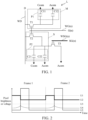
FIG. 1 is a schematic circuit diagram of a pixel circuit according to an embodiment of the present disclosure; -
FIG. 2 is a schematic diagram of pixel brightness change in a case that a sharing switch is turned on later than a primary switch and a secondary switch for 1/4 frame according to the embodiment of the present disclosure; -
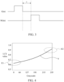
FIG. 3 is a schematic diagram of an interval of time between a scan signal and a sharing scan signal according to an embodiment of the present disclosure; -
FIG. 4 is a schematic diagram of an LCS curve according to an embodiment of the present disclosure. - Technical solutions in the embodiments of the present disclosure will be clearly and completely described below in conjunction with accompanying drawings in embodiments of the present disclosure. Obviously, the described embodiments are only a part of the embodiments of the present disclosure, rather than all the embodiments. Based on the embodiments of the present disclosure, all other embodiments obtained by those skilled in the art without creative work shall fall within a protection scope of the present disclosure.
- In the description herein, it should be understood that the terms such as "center," "longitudinal," "transverse," "length," "width," "thickness," "upper," "lower," "front," "back," "left," "right," "vertical," "horizontal," "top," "bottom," "inner," "outer," "clockwise," and "counterclockwise" indicating a directional or positional relationship are based on orientation or positional relationship shown in the drawings and are only for the convenience of describing the present disclosure and simplifying the description and do not indicate or imply that the device or element referred to has a specific orientation and is constructed and operated in a specific orientation, and therefore it cannot be understood as a limitation to the present disclosure.
- In the description herein, it should be understood that terms "first" and "second" are only used for descriptive purposes, and cannot be understood as indicating or implying relative importance or implicitly indicating the number of indicated technical features. Therefore, features defined with "first" and "second" may explicitly or implicitly include one or more of the features. In the description of the present disclosure, "plurality" means two or more, unless otherwise specifically defined.
- Many different embodiments or examples are provided herein to realize the different structures of the present disclosure. In order to simplify the disclosure of the present disclosure, components and configurations of specific examples are described below. Certainly, they are only examples, and the purpose is not limited to the present disclosure. In addition, the present disclosure may repeat reference numerals and/or reference letters in different examples, and this repetition is used for a purpose of simplification and clarity and itself does not indicate a relationship between the various embodiments and/or configurations discussed. In addition, examples of various specific processes and materials are provided herein, but those skilled in the art may be aware of applications of other processes and/or the use of other materials.
- In the liquid crystal display panel, in order to improve a large viewing-angle color shift effect of a liquid crystal display device (such as a vertical alignment type), pixel units can be designed with low color shift (LCS).
- For example, a first aspect of the present disclosure provides a pixel circuit that can be applied to a liquid crystal display device with a design for low color shift, such as a liquid crystal display device with a multi-domain (such as four-domain or eight-domain) structure, but is not limited to the description here.
- As shown in
FIG. 1 , the pixel circuit includes a plurality of pixel driving modules L for driving a plurality of sub-pixels (such as red, green, and blue sub-pixels). For example, the pixel driving module L includes a primary pixel control assembly M and a secondary pixel control assembly S. For example, the pixel driving module L including the primary pixel control assembly M and the secondary pixel control assembly S can be configured for blue sub-pixels, configured for red sub-pixels, or configured for blue and red sub-pixels, to optimize the display effect, but is not limited to the description here. - As shown in
FIG. 1 , the primary pixel control assembly M may include a primary switch T1 and a primary pixel electrode P1. The primary switch T1 may be configured to be controlled by a scan signal G(n) of a present-stage scan line WG(n) to transfer a data signal D of a data line WD to the primary pixel electrode P1, wherein n is a positive integer that indicates a specific-stage scan configuration in a multi-stage scan architecture. - As shown in
FIG. 1 , the secondary pixel control assembly S may include a secondary switch T2 and a secondary pixel electrode P2. The secondary switch T2 can be configured to be controlled by the scan signal G(n) on the present-stage scan line WG(n) to transfer the data signal D of the data line WD to the secondary pixel electrode P2. - As shown in
FIG. 1 , the pixel driving module may further include a sharing switch T3. The sharing switch T3 may be configured to be controlled by a sharing scan signal SG(n) on a sharing scan line WSG(n) to turn down electric potential at the secondary pixel electrode P2. - The following examples illustrate embodiments of the pixel circuit, but are not limited to the description here.
- For example, as shown in
FIG. 1 , each of the primary switch T1, the secondary switch T2, and the sharing switch T3 is a transistor switch, and the transistor switch includes a control terminal, a first terminal, and a second terminal, such as a gate, a drain, and a source of a thin film transistor (TFT), but not limited to the description here. The control terminal can be controlled by an electrical signal to control conduction between the first terminal and the second terminal so that a signal from the first terminal is transmitted to the second terminal. - As shown in
FIG. 1 , the control terminal of the primary switch T1 is electrically connected to the scan line WG(n), the first terminal of the primary switch T1 is electrically connected to the data line WD, and the second terminal of the primary switch T1 is electrically connected to the primary pixel electrode P1. For example, the primary pixel electrode P1 includes a liquid crystal capacitor C11 and a storage capacitor C12. The liquid crystal capacitor C11 is electrically connected between the second terminal of the primary switch T1 and a first common electrode Ccom. The storage capacitor C12 is electrically connected between the second terminal of the primary switch T1 and a second common electrode Acorn. - As shown in
FIG. 1 , the control terminal of the secondary switch T2 is electrically connected to the scan line WG(n). The first terminal of the secondary switch T2 is electrically connected to the data line D. The second terminal of the secondary switch T2 is electrically connected to the secondary pixel electrode P2. For example, the secondary pixel electrode P2 includes a liquid crystal capacitor C21 and a storage capacitor C22. The liquid crystal capacitor C21 is electrically connected between the second terminal of the secondary switch T2 and the first common electrodes Ccom. The storage capacitor C22 is electrically connected between the second terminal of the secondary switch T2 and the second common electrode Acorn. - As shown in
FIG. 1 , a control terminal of the sharing switch T3 is electrically connected to the sharing scan line WSG(n). A first terminal of the sharing switch T3 is electrically connected to the secondary pixel electrode P2 (for example, the liquid crystal capacitor C21 and the storage capacitor C22) and a second terminal of the secondary switch T2. A second terminal of the sharing switch T3 is electrically connected to the second common electrode Acorn. - As shown in
FIG. 1 , during a display process, a scanning signal G(n) on the present-stage scanning line WG(n) can control the primary switch T1 and the secondary switch T2 to be turned on (ON). Meanwhile, the sharing scan signal SG(n) on the sharing scan line WSG(n) controls the sharing switch T3 to be turned off (OFF). The data signal D of the data line WD is transmitted to the primary pixel electrode P1 and the secondary pixel electrode P2, to make the primary pixel electrode P1 (such as the liquidcrystal capacitor C1 1 and the storage capacitor C12) and the secondary pixel electrode P2 (such as the liquid crystal capacitor C21 and the storage capacitor C22) charge to the same electric potential (for example, high electric potential). Then, the scan signal G(n) on the present-stage scan line WG(n) controls the primary switch T1 and the secondary switch T2 to be turned off. Meanwhile, the sharing scan signal SG(n) on the sharing scan line WSG(n) controls the sharing switch T3 to be turned on. So, the electric potentials of the primary pixel electrode P1 and the secondary pixel electrode P2 are different. For example, the secondary pixel electrode P2 is discharged to the second common electrode Acom through the sharing switch T3 to make the electric potential at the secondary pixel electrode P2 lower than the electric potential at the primary pixel electrode P1. - Optionally, in an embodiment, as shown in
FIG. 1 , each of the primary switch T1, the secondary switch T2, and the sharing switch T3 is a transistor switch. The transistor switch includes a control terminal, a first terminal, and a second terminal. The control terminal of the primary switch T1 and the control terminal of the secondary switch T2 are electrically connected to the scan line WG(n), and the control terminal of the sharing switch T3 is electrically connected to the sharing scan line WSG(n). Therefore, the control terminal of the sharing switch can be controlled independently of the control terminal of the primary switch and the control terminal of the secondary switch, so as to regulate a brightness ratio between the primary pixel electrode and the secondary pixel electrode. - Optionally, in an embodiment, as shown in
FIG. 1 , a first terminal of the sharing switch T3 is electrically connected to the secondary pixel electrode P2 and a second terminal of the secondary switch T2. The second terminal of the sharing switch is electrically connected to a common electrode. Therefore, the secondary pixel electrode is discharged through the sharing switch, so that the electric potential at the secondary pixel electrode is lower than the electric potential at the primary pixel electrode, so as to improve the viewing-angle. - Optionally, in an embodiment, as shown in
FIG. 1 , each of the primary pixel electrode P1 and the secondary pixel electrode P2 includes a liquid crystal capacitor (such as C11, C21) and a storage capacitor (such as C12, C22). The liquid crystal capacitor C21 of the secondary pixel electrode P2 is electrically connected to the second terminal of the secondary switch T2 and a first common electrode Ccom. The storage capacitor C22 of the secondary pixel electrode P2 is electrically connected to the second terminal of the secondary switch T2 and a second common electrode Acorn. A second terminal of the sharing switch T3 is electrically connected to the second common electrode Acorn. Therefore, the secondary pixel electrode is discharged to the second common electrode through the sharing switch, so that the electric potential at the primary pixel electrode is different from the electric potential at the secondary pixel electrode, so as to appropriately adjust the difference in the deflection angle of the liquid crystal. - Optionally, in an embodiment, as shown in
FIG. 1 , the sharing switch T3 is configured to be turned on to reduce the electric potential at the secondary pixel electrode P2. Therefore, the electric potential at the secondary pixel electrode is lower than the electric potential at the primary pixel electrode, so that the electric potential at the primary pixel electrode is different from the electric potential at the secondary pixel electrode, and the large viewing-angle deviation phenomenon of the liquid crystal display device can be improved. - Optionally, in an embodiment, as shown in
FIG. 1 , the present-stage scan line WG(n) and the sharing scan line WSG(n) are insulated from each other. For example, the present-stage scan line WG(n) and the sharing scan line WSG(n) are disposed at two metal material layers, and an insulating layer is disposed between the two metal material layers to avoid mutual interference of control signals. Therefore, the scan signal on the present-stage scan line and the sharing scan signal on the sharing scan line can be independent of each other. a length of time between the sharing scan signal and the scan signal can be adjusted in a time-division manner in order to flexibly adjust the electric potential and brightness ratio of the sub-pixel electrode and the main pixel electrode. - It should be noted that the length of time that the electric potential at the secondary pixel electrode is at a high electric potential and at a low electric potential is adjustable (time division) so that low color shift (LCS) characteristic parameters (e.g., the ratio of the brightness of the secondary pixel electrode to the brightness of the primary pixel electrode) can be flexibly adjusted.
- For example, the pixel brightness that the sharing switch is turned on 1/4 frame later than the primary switch and the secondary switch is taken as an example,
FIG. 2 is a schematic diagram of a pixel brightness change when the sharing switch is turned on 1/4 frame later than the primary switch and the secondary switch. The pixel brightness or voltage expressed on the vertical axis is positively correlated, and time is expressed on the horizontal axis. InFIG. 2 , a time length of two-frame is taken as an example, wherein U1 represents a brightness curve of the primary pixel electrode generating high grayscale when the primary switch is turned on so that the primary pixel electrode maintains a high level (for example, 14 volts); U2 represents a brightness curve of the secondary pixel electrode generating high grayscale when the secondary pixel electrode is turned on and off so that the secondary pixel electrode has a pulse with a high-level; U3 represents a brightness curve of the primary pixel electrode generating low grayscale when the primary pixel electrode is turned on so that the primary pixel electrode maintains a low level (such as 0.2 volt); U4 represents a brightness curve of the secondary pixel electrode generating low grayscale when the secondary switch is turned on and off so that the secondary pixel electrode is charged and discharged; and U5 represents a voltage curve that the sharing switch is turned on 1/4 frame later than the primary switch and the secondary switch. - In
FIG. 2 , as shown by the curve U1, the primary pixel electrode maintains high brightness as the grayscale is high; as shown by the curve U3, the primary pixel electrode maintains low brightness as the grayscale is low. - In
FIG. 2 , as shown by curves U2 and U5, when the secondary switch is turned on (e.g., the high level as shown by curve U2) and the sharing switch is turned off (e.g., the low level as shown by curve U5), the secondary pixel electrode maintains high brightness as the grayscale is high (e.g., as shown by curve U2). When the secondary switch is turned off (e.g., the low level as shown by curve U2) and the sharing switch is turned on (e.g., the high level as shown by curve U5), the secondary pixel electrode maintains low brightness when the gray scale is high (e.g., as shown by the curve U2), so that the brightness of the secondary pixel electrode is different from the brightness of the primary pixel electrode. - It should be noted that after the sharing switch is turned on, a voltage of the secondary pixel electrode is reduced to produce a brightness change, but a frequency of the brightness change is consistent with a refresh frequency of the display panel, in which a brightness change frequency of a flickering picture is not like at twice the refresh frequency of the display panel. Therefore, the brightness change after the sharing switch is turned on will not cause an obvious flicker.
- In
FIG. 2 , as shown by curves U4 and U5, after the sharing switch is turned on, in another frame (e.g., aframe 2 inFIG. 2 ), the secondary switch is turned on (e.g., the high level as shown by curve U2) and the sharing switch is turned off (e.g., the low level as shown by the curve U5), because the liquid crystals react slowly at the low grayscale, the brightness of the secondary pixel electrode at the low grayscale gradually increases (e.g., as shown by the curve U4). When the brightness of the secondary pixel electrode has not reached the brightness of the primary pixel electrode, the secondary switch is turned off and the sharing switch is turned on (e.g., the high level as shown by the curve U5), to cause that the secondary pixel electrode starts to discharge, and the brightness of the secondary pixel electrode at the low grayscale gradually decreases (e.g., as shown by the curve U4), resulting in that the brightness of the secondary pixel electrode at the low grayscale is lower. Thus, a characteristic parameter of the LCS of the low grayscale is lower than a characteristic parameter of the LCS of the high grayscale, so that a characteristic curve of the LCS shows an upward trend. - In
FIG. 2 , as shown by the curves U2, U4, and U5, after the sharing switch is turned on, the voltage of the secondary pixel electrode drops, so that the brightness of the secondary pixel electrode decreases. Because the characteristic parameter of the LCS is a ratio of the brightness of the secondary pixel electrode to the brightness of the primary pixel electrode, by adjusting the time when the sharing switch is turned on, the brightness of the secondary pixel electrode can be adjusted, and in turn, the characteristic parameter of the LCS parameter can be adjusted. - It should be noted that, as shown in
FIG. 1 , because the present-stage scan line WG(n) and the sharing scan line WSG(n) are insulated from each other, the scan signal G(n) of the present-stage scan line WG(n) and the sharing scan signal SG(n) on the sharing scan line WSG(n) are delivered separately, so that time for turning-on the sharing switch T3 can be independently controlled. - For example, as shown in
FIGs. 1 and3 , after a pulse of the scan signal G(n) on the present-stage scan line WG(n) changes from a high level to a low level, and after an interval of time t, the pulse of the sharing scan signal SG(n) on the sharing scan line WSG(n) changes from the low level to the high level, so that when the secondary pixel electrode P2 maintains the high level, after the interval of time t, the electric potential at the secondary pixel electrode P2 is controlled to be decreased. The electric potential at the secondary pixel electrode P2 is lower than the electric potential at the primarypixel electrode P 1, so that the electric potential at the primary pixel electrode P1 and the electric potential at the secondary pixel electrode P2 are different, to appropriately adjust the difference of the liquid crystal deflection angle, thereby improving the viewing-angle and a large viewing-angle color shift effect of the liquid crystal display device. - Optionally, in an embodiment, as shown in
FIGs. 1 and3 , the scan signal G(n) on the scan line WG(n) is configured to have a first positive-level pulse, and the sharing scan signal SG(n) on the sharing scan line WSG(n) is configured to have a second positive-level pulse. The second positive-level pulse is later than the first positive-level pulse. There is an interval of time between the first positive-level pulse and the second positive-level pulse. Therefore, by adjusting the interval of time, the electric potential and brightness ratio between the primary pixel electrode and the secondary pixel electrode can be adjusted. - In addition, a second aspect of the present disclosure provides a display device, such as a liquid crystal display device with a low color shift architecture. The display device includes the pixel circuit as described above. The implementation details of the pixel circuit can be referred to the embodiments mentioned above and will not be repeatedly described.
- It should be noted that, in the pixel circuit and display device of the above-mentioned embodiments of the present disclosure, the time of turning on and off of the sharing switch is independently controlled, so that the display process of the sub-pixels has a time-division effect. As shown in
FIG. 4 , an adjustable range of a rising trend of an LCS curve V can be greatly increased. In a low grayscale range (as shown in a range E1), an LCS characteristic parameter is lower, and the viewing-angle effect is better; in the high grayscale range, the LCS characteristic parameter is higher (as shown in a range E2), the penetration effect is better, which can simultaneously meet the low grayscale viewing-angle and high grayscale penetration requirements of the display device. Therefore, the pixel circuit and the display device of the above-mentioned embodiments of the present disclosure can improve problems derived from a downward trend of the LCS curve or the limited adjustable range of the prior art, such as a limited viewing-angle and limited transmittance. - In the pixel circuit and the display device of the above embodiment of the present disclosure, the primary switch is configured to be controlled by the scan signal on the present-stage scan line to transmit the data signal on the data line to the primary pixel electrode, and the secondary switch is configured to be controlled by the scan signal on the present-stage scan line to transmit the data signal on the data line to the secondary pixel electrode, and the sharing switch is configured to be controlled by the sharing scan signal on the sharing scan line to reduce the electric potential at the secondary pixel electrode. Therefore, the electric potential at the primary pixel electrode is different from the electric potential at the secondary pixel electrode, in which the adjustable range of the LCS curve is greatly increased. Meanwhile, it can simultaneously meet a low grayscale viewing-angle and high grayscale penetration requirements of the display device for proper adjustment to a difference of a liquid crystal deflection angle. Meanwhile, meeting the low grayscale viewing-angle and high grayscale penetration requirements of the display device can improve the viewing-angle and improve a large viewing-angle color shift effect of the liquid crystal display device.
- The embodiments of the present disclosure are described in detail above, and specific examples are used herein to illustrate the principles and implementation of the present disclosure. The descriptions of the above embodiments are only used to help understand the technical solutions and core ideas of the present disclosure. Those skilled in the art should understand that they can still modify the technical solutions recorded in the previous embodiments or equivalently replace some technical features. However, these modifications or replacements do not cause the essence of the corresponding technical solutions to deviate from the scope of the technical solutions of the embodiments of the present disclosure.
Claims (17)
- A pixel circuit, comprising:
a plurality of pixel driving modules, wherein each of the pixel driving modules comprises:a primary pixel control assembly comprising a primary switch and a primary pixel electrode, wherein the primary switch is configured to be controlled by a scan signal on a present-stage scan line to transfer a data signal on a data line to the primary pixel electrode;a secondary pixel control assembly comprising a secondary switch and a secondary pixel electrode, wherein the secondary switch is configured to be controlled by the scan signal on the present-stage scan line to transmit the data signal on the data line to the secondary pixel electrode; anda sharing switch configured to be controlled by a sharing scan signal on a sharing scan line to reduce the electric potential at the secondary pixel electrode;wherein the present-stage scan line and the sharing scan line are insulated from each other; and the scan signal on the scan line is configured to have a first positive-level pulse, and the sharing scan signal on the sharing scan line is configured to have a second positive-level pulse, the second positive-level pulse is later than the first positive-level pulse, and there is an interval of time between the first positive-level pulse and the second positive-level pulse. - The pixel circuit as claimed in claim 1, wherein each of the primary switch, the secondary switch, and the sharing switch is a transistor switch comprising a control terminal, a first terminal, and a second terminal, the control terminal of the primary switch and the control terminal of the secondary switch are electrically connected to the scan line, and the control terminal of the sharing switch is electrically connected to the sharing scan line.
- The pixel circuit of claim 2, wherein the first terminal of the sharing switch is electrically connected to the secondary pixel electrode and the second terminal of the secondary switch, and the second terminal of the sharing switch is electrically connected to a common electrode.
- The pixel circuit as claimed in claim 3, wherein each of the primary pixel electrode and the secondary pixel electrode comprises a liquid crystal capacitor and a storage capacitor, the liquid crystal capacitor of the secondary pixel electrode is electrically connected to the second terminal of the secondary switch and a first common electrode, the storage capacitor of the secondary pixel electrode is electrically connected to the second terminal of the secondary switch and a second common electrode, and the second terminal of the sharing switch is electrically connected to the second common electrode.
- The pixel circuit as claimed in claim 1, wherein the present-stage scan line and the sharing scan line are disposed in two metal material layers, and an insulation layer is disposed between the two metal material layers.
- The pixel circuit of claim 1, wherein the sharing switch is configured to be turned on to reduce the electric potential at the secondary pixel electrode.
- The pixel circuit of claim 1, wherein the pixel driving module is configured for blue sub-pixels, configured for red sub-pixels, or configured for blue and red sub-pixels.
- A pixel circuit, comprising:
a plurality of pixel driving modules, wherein each of the pixel driving modules comprises:a primary pixel control assembly comprising a primary switch and a primary pixel electrode, wherein the primary switch is configured to be controlled by a scan signal on a present-stage scan line to transfer a data signal on a data line to the primary pixel electrode;a secondary pixel control assembly comprising a secondary switch and a secondary pixel electrode, wherein the secondary switch is configured to be controlled by the scan signal on the present-stage scan line to transmit the data signal on the data line to the secondary pixel electrode; anda sharing switch configured to be controlled by a sharing scan signal on a sharing scan line to reduce the electric potential at the secondary pixel electrode. - The pixel circuit as claimed in claim 8, wherein each of the primary switch, the secondary switch, and the sharing switch is a transistor switch comprising a control terminal, a first terminal, and a second terminal, the control terminal of the primary switch and the control terminal of the secondary switch are electrically connected to the scan line, and the control terminal of the sharing switch is electrically connected to the sharing scan line.
- The pixel circuit as claimed in claim 9, wherein the first terminal of the sharing switch is electrically connected to the secondary pixel electrode and the second terminal of the secondary switch, and the second terminal of the sharing switch is electrically connected to a common electrode.
- The pixel circuit as claimed in claim 10, wherein each of the primary pixel electrode and the secondary pixel electrode comprises a liquid crystal capacitor and a storage capacitor, the liquid crystal capacitor of the secondary pixel electrode is electrically connected to the second terminal of the secondary switch and a first common electrode, the storage capacitor of the secondary pixel electrode is electrically connected to the second terminal of the secondary switch and a second common electrode, and the second terminal of the sharing switch is electrically connected to the second common electrode.
- The pixel circuit as claimed in claim 8, wherein the present-stage scan line and the sharing scan line are insulated from each other.
- The pixel circuit as claimed in claim 8, wherein the present-stage scan line and the sharing scan line are disposed in two metal material layers, and an insulation layer is disposed between the two metal material layers.
- The pixel circuit as claimed in claim 8, wherein the sharing switch is configured to be turned on to reduce the electric potential at the secondary pixel electrode.
- The pixel circuit as claimed in claim 8, wherein the scan signal on the scan line is configured to have a first positive-level pulse, and the sharing scan signal on the sharing scan line is configured to have a second positive-level pulse, the second positive-level pulse is later than the first positive-level pulse, and there is an interval of time between the first positive-level pulse and the second positive-level pulse.
- The pixel circuit as claimed in claim 8, wherein the pixel driving module is configured for blue sub-pixels, configured for red sub-pixels, or configured for blue and red sub-pixels.
- A display device comprising the pixel circuit as claimed in claim 8.
Applications Claiming Priority (2)
| Application Number | Priority Date | Filing Date | Title |
|---|---|---|---|
| CN202111263202.1A CN113990266A (en) | 2021-10-28 | 2021-10-28 | Pixel circuit and display device |
| PCT/CN2021/128761 WO2023070720A1 (en) | 2021-10-28 | 2021-11-04 | Pixel circuit and display apparatus |
Publications (2)
| Publication Number | Publication Date |
|---|---|
| EP4425477A1 true EP4425477A1 (en) | 2024-09-04 |
| EP4425477A4 EP4425477A4 (en) | 2025-08-20 |
Family
ID=79743439
Family Applications (1)
| Application Number | Title | Priority Date | Filing Date |
|---|---|---|---|
| EP21819316.7A Pending EP4425477A4 (en) | 2021-10-28 | 2021-11-04 | PIXEL CIRCUIT AND DISPLAY DEVICE |
Country Status (6)
| Country | Link |
|---|---|
| US (1) | US12020662B2 (en) |
| EP (1) | EP4425477A4 (en) |
| JP (1) | JP7635153B2 (en) |
| KR (2) | KR102908622B1 (en) |
| CN (1) | CN113990266A (en) |
| WO (1) | WO2023070720A1 (en) |
Families Citing this family (1)
| Publication number | Priority date | Publication date | Assignee | Title |
|---|---|---|---|---|
| CN120722620B (en) * | 2025-08-19 | 2025-11-28 | 惠科股份有限公司 | Array substrate, display panel and control method |
Family Cites Families (23)
| Publication number | Priority date | Publication date | Assignee | Title |
|---|---|---|---|---|
| DE2144744C3 (en) * | 1971-09-07 | 1974-07-11 | Robert Bosch Fernsehanlagen Gmbh, 6100 Darmstadt | Method and circuit arrangement for the automatic correction of grid registration errors in color television cameras |
| JP3767877B2 (en) * | 1997-09-29 | 2006-04-19 | 三菱化学株式会社 | Active matrix light emitting diode pixel structure and method thereof |
| JP4438665B2 (en) * | 2005-03-29 | 2010-03-24 | シャープ株式会社 | Liquid crystal display |
| JP2008083320A (en) | 2006-09-27 | 2008-04-10 | Seiko Epson Corp | Electro-optical device, driving method thereof, and electronic apparatus |
| TWI364609B (en) * | 2007-02-16 | 2012-05-21 | Chimei Innolux Corp | Liquid crystal display panel and manufacturing method thereof |
| JP4583465B2 (en) * | 2008-03-25 | 2010-11-17 | 株式会社日立製作所 | Plasma display panel driving method and plasma display apparatus |
| KR20110101917A (en) * | 2010-03-10 | 2011-09-16 | 삼성전자주식회사 | Liquid crystal display |
| KR101817791B1 (en) * | 2010-12-14 | 2018-01-12 | 삼성디스플레이 주식회사 | Liquid crystal display device |
| TWI452559B (en) * | 2011-11-14 | 2014-09-11 | Au Optronics Corp | Display panel and driving method thereof |
| CN103278977B (en) * | 2013-05-31 | 2015-11-25 | 深圳市华星光电技术有限公司 | Display panels and dot structure thereof and driving method |
| US9082361B2 (en) * | 2013-10-12 | 2015-07-14 | Shenzhen China Star Optoelectronics Technology Co., Ltd. | Polarized three-dimensional display panel and pixel cell thereof |
| CN104216187B (en) * | 2014-09-04 | 2017-08-15 | 深圳市华星光电技术有限公司 | Dot structure, liquid crystal display panel and its driving method |
| CN104360555B (en) * | 2014-11-21 | 2017-06-06 | 深圳市华星光电技术有限公司 | A kind of liquid crystal display panel and its driving method, liquid crystal display device |
| CN104483792B (en) * | 2014-12-26 | 2017-04-12 | 深圳市华星光电技术有限公司 | Array substrate and display device |
| CN107710320B (en) * | 2015-06-23 | 2020-04-17 | 堺显示器制品株式会社 | Liquid crystal display device and method for driving liquid crystal display device |
| US10140940B2 (en) * | 2015-07-24 | 2018-11-27 | Japan Display Inc. | Display device |
| CN107924662A (en) * | 2015-08-27 | 2018-04-17 | 堺显示器制品株式会社 | Liquid crystal display device |
| CN105204249B (en) * | 2015-10-29 | 2018-07-17 | 深圳市华星光电技术有限公司 | Scan drive circuit in array substrate and array substrate |
| CN107132676B (en) * | 2017-05-15 | 2021-03-02 | Tcl华星光电技术有限公司 | Visual angle mode switching method of liquid crystal display device and liquid crystal display device |
| CN107818770A (en) * | 2017-10-25 | 2018-03-20 | 惠科股份有限公司 | Driving device and method of display panel |
| WO2020012655A1 (en) * | 2018-07-13 | 2020-01-16 | 堺ディスプレイプロダクト株式会社 | Control device and liquid crystal display device |
| CN110376810A (en) | 2019-06-10 | 2019-10-25 | 惠科股份有限公司 | Display panel, bright spot repairing method of display panel and display device |
| CN111176041A (en) * | 2020-02-21 | 2020-05-19 | Tcl华星光电技术有限公司 | Pixel structure and pixel circuit |
-
2021
- 2021-10-28 CN CN202111263202.1A patent/CN113990266A/en active Pending
- 2021-11-04 KR KR1020247016621A patent/KR102908622B1/en active Active
- 2021-11-04 KR KR1020227001300A patent/KR102668912B1/en active Active
- 2021-11-04 WO PCT/CN2021/128761 patent/WO2023070720A1/en not_active Ceased
- 2021-11-04 EP EP21819316.7A patent/EP4425477A4/en active Pending
- 2021-11-04 JP JP2021566502A patent/JP7635153B2/en active Active
- 2021-11-04 US US17/618,484 patent/US12020662B2/en active Active
Also Published As
| Publication number | Publication date |
|---|---|
| EP4425477A4 (en) | 2025-08-20 |
| WO2023070720A1 (en) | 2023-05-04 |
| JP7635153B2 (en) | 2025-02-25 |
| JP2023550848A (en) | 2023-12-06 |
| KR20230062464A (en) | 2023-05-09 |
| US20240013742A1 (en) | 2024-01-11 |
| KR20240090560A (en) | 2024-06-21 |
| US12020662B2 (en) | 2024-06-25 |
| KR102908622B1 (en) | 2026-01-08 |
| KR102668912B1 (en) | 2024-05-24 |
| CN113990266A (en) | 2022-01-28 |
Similar Documents
| Publication | Publication Date | Title |
|---|---|---|
| US8884861B2 (en) | Liquid crystal display and driving method thereof | |
| CN101960371B (en) | Active matrix substrate, liquid crystal panel, liquid crystal display device, liquid crystal display unit, and television receiver | |
| US8237646B2 (en) | Display apparatus and method of driving the same | |
| CN105372886B (en) | Liquid crystal display | |
| US8179489B2 (en) | Display device | |
| US8587580B2 (en) | Liquid crystal display | |
| US10283061B2 (en) | Pixel structure, array substrate, and display panel | |
| US8436805B2 (en) | Active matrix substrate, liquid crystal panel, liquid crystal display unit, liquid crystal display device, and television receiver | |
| CN111048051A (en) | Display panel | |
| JP2007086791A (en) | Liquid crystal panel, driving method thereof, and liquid crystal display device using the same | |
| WO2018121303A1 (en) | Liquid crystal display and method for driving same | |
| US10600382B2 (en) | Array substrate, data driving circuit, data driving method and display apparatus | |
| CN104464680B (en) | A kind of array base palte and display device | |
| US20130278874A1 (en) | Liquid crystal display | |
| US8766889B2 (en) | Liquid crystal display and driving method thereof | |
| CN108389557A (en) | Display device and its driving method | |
| US20120206436A1 (en) | Liquid crystal display device and method for driving liquid crystal display device | |
| US20130135360A1 (en) | Display device and driving method thereof | |
| CN100374946C (en) | Liquid crystal panel with uniform brightness, liquid crystal display using same and driving method thereof | |
| US12020662B2 (en) | Pixel circuit and display device | |
| US20230314886A1 (en) | Array substrate, liquid crystal display panel, and display device | |
| US20150293413A1 (en) | Thin-film transistor array substrate and liquid crystal display device | |
| CN114815419A (en) | Pixel structure and display panel | |
| US9041637B2 (en) | Display device including switching elements and method for driving the display device | |
| US20080192042A1 (en) | Circuit for Generating Driving Voltages, Display Device Using the Same, and Method of Generating Driving Voltages |
Legal Events
| Date | Code | Title | Description |
|---|---|---|---|
| STAA | Information on the status of an ep patent application or granted ep patent |
Free format text: STATUS: UNKNOWN |
|
| STAA | Information on the status of an ep patent application or granted ep patent |
Free format text: STATUS: THE INTERNATIONAL PUBLICATION HAS BEEN MADE |
|
| PUAI | Public reference made under article 153(3) epc to a published international application that has entered the european phase |
Free format text: ORIGINAL CODE: 0009012 |
|
| STAA | Information on the status of an ep patent application or granted ep patent |
Free format text: STATUS: REQUEST FOR EXAMINATION WAS MADE |
|
| 17P | Request for examination filed |
Effective date: 20211214 |
|
| AK | Designated contracting states |
Kind code of ref document: A1 Designated state(s): AL AT BE BG CH CY CZ DE DK EE ES FI FR GB GR HR HU IE IS IT LI LT LU LV MC MK MT NL NO PL PT RO RS SE SI SK SM TR |
|
| DAV | Request for validation of the european patent (deleted) | ||
| DAX | Request for extension of the european patent (deleted) | ||
| A4 | Supplementary search report drawn up and despatched |
Effective date: 20250722 |
|
| RIC1 | Information provided on ipc code assigned before grant |
Ipc: G09G 3/36 20060101AFI20250716BHEP |