EP4421989A1 - Feed pin, and patch antenna comprising same - Google Patents
Feed pin, and patch antenna comprising same Download PDFInfo
- Publication number
- EP4421989A1 EP4421989A1 EP22883840.5A EP22883840A EP4421989A1 EP 4421989 A1 EP4421989 A1 EP 4421989A1 EP 22883840 A EP22883840 A EP 22883840A EP 4421989 A1 EP4421989 A1 EP 4421989A1
- Authority
- EP
- European Patent Office
- Prior art keywords
- area
- feed
- stepped plate
- plate
- patch
- Prior art date
- Legal status (The legal status is an assumption and is not a legal conclusion. Google has not performed a legal analysis and makes no representation as to the accuracy of the status listed.)
- Pending
Links
- 239000004020 conductor Substances 0.000 claims abstract description 61
- 238000005476 soldering Methods 0.000 claims abstract description 41
- 238000010030 laminating Methods 0.000 claims description 10
- 239000000758 substrate Substances 0.000 description 19
- 238000009863 impact test Methods 0.000 description 8
- 238000000034 method Methods 0.000 description 6
- 238000005260 corrosion Methods 0.000 description 5
- 230000007797 corrosion Effects 0.000 description 5
- 239000000919 ceramic Substances 0.000 description 4
- RYGMFSIKBFXOCR-UHFFFAOYSA-N Copper Chemical compound [Cu] RYGMFSIKBFXOCR-UHFFFAOYSA-N 0.000 description 2
- BQCADISMDOOEFD-UHFFFAOYSA-N Silver Chemical compound [Ag] BQCADISMDOOEFD-UHFFFAOYSA-N 0.000 description 2
- XAGFODPZIPBFFR-UHFFFAOYSA-N aluminium Chemical compound [Al] XAGFODPZIPBFFR-UHFFFAOYSA-N 0.000 description 2
- 229910052782 aluminium Inorganic materials 0.000 description 2
- QVGXLLKOCUKJST-UHFFFAOYSA-N atomic oxygen Chemical compound [O] QVGXLLKOCUKJST-UHFFFAOYSA-N 0.000 description 2
- 229910052802 copper Inorganic materials 0.000 description 2
- 239000010949 copper Substances 0.000 description 2
- 230000000593 degrading effect Effects 0.000 description 2
- PCHJSUWPFVWCPO-UHFFFAOYSA-N gold Chemical compound [Au] PCHJSUWPFVWCPO-UHFFFAOYSA-N 0.000 description 2
- 229910052737 gold Inorganic materials 0.000 description 2
- 239000010931 gold Substances 0.000 description 2
- 239000000696 magnetic material Substances 0.000 description 2
- 229910052760 oxygen Inorganic materials 0.000 description 2
- 239000001301 oxygen Substances 0.000 description 2
- 238000007665 sagging Methods 0.000 description 2
- 229910052709 silver Inorganic materials 0.000 description 2
- 239000004332 silver Substances 0.000 description 2
- 238000004891 communication Methods 0.000 description 1
- 230000003247 decreasing effect Effects 0.000 description 1
- 230000000694 effects Effects 0.000 description 1
- 239000012634 fragment Substances 0.000 description 1
- 238000009434 installation Methods 0.000 description 1
- 229910000859 α-Fe Inorganic materials 0.000 description 1
Images




Classifications
-
- H—ELECTRICITY
- H01—ELECTRIC ELEMENTS
- H01Q—ANTENNAS, i.e. RADIO AERIALS
- H01Q1/00—Details of, or arrangements associated with, antennas
- H01Q1/12—Supports; Mounting means
- H01Q1/22—Supports; Mounting means by structural association with other equipment or articles
-
- H—ELECTRICITY
- H01—ELECTRIC ELEMENTS
- H01Q—ANTENNAS, i.e. RADIO AERIALS
- H01Q9/00—Electrically-short antennas having dimensions not more than twice the operating wavelength and consisting of conductive active radiating elements
- H01Q9/04—Resonant antennas
- H01Q9/0407—Substantially flat resonant element parallel to ground plane, e.g. patch antenna
- H01Q9/0428—Substantially flat resonant element parallel to ground plane, e.g. patch antenna radiating a circular polarised wave
-
- H—ELECTRICITY
- H01—ELECTRIC ELEMENTS
- H01Q—ANTENNAS, i.e. RADIO AERIALS
- H01Q1/00—Details of, or arrangements associated with, antennas
- H01Q1/44—Details of, or arrangements associated with, antennas using equipment having another main function to serve additionally as an antenna, e.g. means for giving an antenna an aesthetic aspect
- H01Q1/46—Electric supply lines or communication lines
-
- H—ELECTRICITY
- H01—ELECTRIC ELEMENTS
- H01Q—ANTENNAS, i.e. RADIO AERIALS
- H01Q9/00—Electrically-short antennas having dimensions not more than twice the operating wavelength and consisting of conductive active radiating elements
- H01Q9/04—Resonant antennas
- H01Q9/0407—Substantially flat resonant element parallel to ground plane, e.g. patch antenna
-
- H—ELECTRICITY
- H01—ELECTRIC ELEMENTS
- H01Q—ANTENNAS, i.e. RADIO AERIALS
- H01Q9/00—Electrically-short antennas having dimensions not more than twice the operating wavelength and consisting of conductive active radiating elements
- H01Q9/04—Resonant antennas
- H01Q9/0407—Substantially flat resonant element parallel to ground plane, e.g. patch antenna
- H01Q9/0414—Substantially flat resonant element parallel to ground plane, e.g. patch antenna in a stacked or folded configuration
-
- H—ELECTRICITY
- H01—ELECTRIC ELEMENTS
- H01Q—ANTENNAS, i.e. RADIO AERIALS
- H01Q9/00—Electrically-short antennas having dimensions not more than twice the operating wavelength and consisting of conductive active radiating elements
- H01Q9/04—Resonant antennas
- H01Q9/0407—Substantially flat resonant element parallel to ground plane, e.g. patch antenna
- H01Q9/045—Substantially flat resonant element parallel to ground plane, e.g. patch antenna with particular feeding means
-
- H—ELECTRICITY
- H01—ELECTRIC ELEMENTS
- H01Q—ANTENNAS, i.e. RADIO AERIALS
- H01Q1/00—Details of, or arrangements associated with, antennas
- H01Q1/27—Adaptation for use in or on movable bodies
- H01Q1/32—Adaptation for use in or on road or rail vehicles
- H01Q1/3208—Adaptation for use in or on road or rail vehicles characterised by the application wherein the antenna is used
- H01Q1/3233—Adaptation for use in or on road or rail vehicles characterised by the application wherein the antenna is used particular used as part of a sensor or in a security system, e.g. for automotive radar, navigation systems
Definitions
- the present disclosure relates to a feed pin for feeding a patch antenna mounted in a vehicle or the like, and the patch antenna including the same.
- patch antennas are installed in vehicles, drones, and information and communication terminals to transmit and receive signals in frequency bands, such as a global positioning system (GPS) and a global navigation satellite system (GNSS).
- GPS global positioning system
- GNSS global navigation satellite system
- a patch antenna includes a dielectric formed in a predetermined thickness, a planar upper patch laminated on an upper surface of the dielectric and acts as an antenna, a lower patch laminated on a lower surface of the dielectric, and a feed pin for feeding the upper patch.
- the dielectric mainly uses ceramic, which is widely used as a high-frequency component due to the excellent characteristics, such as a high dielectric constant and a low thermal expansion coefficient
- the patch antenna is also referred to as a ceramic patch antenna.
- the upper patch and the lower patch are formed in various shapes, such as a quadrangular, circular, elliptical, triangular, or ring shape, but a quadrangular or circular shape is mainly used.
- the upper patch and the lower patch are made of a conductive material with a high conductivity with the ceramic dielectric. Structures of the upper patch and the lower patch include a multilayer, a bulk type, and the like.
- the feed pin is electrically connected to the upper patch through soldering to feed the upper patch.
- the patch antenna has a problem in that a corrosion phenomenon occurs in a soldering layer due to the reaction between lead and oxygen as high or low temperatures are repeated during an electrical reliability test (i.e., an electrical thermal impact test) for vehicle installation.
- the patch antenna has a problem in that micro cracks easily occur even with a small amount of stress (impact) due to the corrosion phenomenon in a soldering area, and the characteristics of the patch antenna are changed due to the micro cracks, thereby degrading reliability.
- the present disclosure has been proposed to solve the problems and is directed to providing a feed pin that prevents cracks occurring in a soldering layer by forming a step on a head, and a patch antenna including the same.
- a feed pin includes a feed head made of a plate-shaped conductive material with a first area, a stepped plate made of a plate-shaped conductive material having a second area and connected to a lower surface of the feed head, and a feed bar made of a polyhedral conductive material and connected to a lower surface of the stepped plate.
- the second area that is an area of a horizontal cross section of the stepped plate may be formed to be smaller than the first area that is a horizontal cross section of the feed head, and a first step may be formed between the feed head and the stepped plate.
- the first step may be formed along the lower surface of the feed head and outer perimeters of side surfaces of the stepped plate.
- the stepped plate may be formed by laminating a plurality of plate-shaped conductors formed to have different horizontal cross-sectional areas, and one or more steps may be formed on side surfaces of the stepped plate. Therefore, a first step formed between the feed head and the stepped plate may include two or more steps.
- a third area that is an area of a horizontal cross section of the feed bar may be formed to be smaller than the second area that is a horizontal cross section of the stepped plate, and a second step may be formed between the stepped plate and the feed bar.
- a first area connected to the feed bar and a second area that is an outer perimetric area of the first area may be defined on the lower surface of the stepped plate, and a plurality of bonding protrusions may be formed in the second area.
- a first area connected to the feed bar and a second area that is an outer perimetric area of the first area may be defined on the lower surface of the stepped plate, and an inclined portion having inclination closer to an upper surface of the feed head toward an outer perimeter of the feed head may be formed in the second area.
- the feed bar may include a first bar disposed on the lower surface of the stepped plate, and a second bar disposed on a lower surface of the first bar, and the second bar may be formed to have a horizontal cross section smaller than a horizontal cross section of the first bar to form a locking stopper.
- a patch antenna includes a dielectric layer, an upper patch disposed on an upper surface of the dielectric layer, a lower patch disposed on a lower surface of the dielectric layer, and a feed pin passing through the upper patch, the dielectric layer, and the lower patch to feed the upper patch, wherein the feed bar includes a feed head made of a plate-shaped conductive material with a first area, a stepped plate made of a plate-shaped conductive material having a second area and connected to a lower surface of the feed head, and a feed bar made of a polyhedral conductive material and connected to a lower surface of the stepped plate.
- a bonding space surrounded by a lower surface of the feed head, an outer perimeter of the stepped plate, and an upper surface of the upper patch is defined in the patch antenna according to the embodiment of the present disclosure, and a soldering layer may be formed in the bonding space.
- the second area that is an area of a horizontal cross section of the stepped plate may be formed to be smaller than the first area that is a horizontal cross section of the feed head, and a first step is formed between the feed head and the stepped plate, and a soldering layer may be formed in a bonding space formed by the first step and an upper surface of the upper patch.
- a first area connected to the feed bar and a second area that is an outer perimetric area of the first area may be defined on the lower surface of the stepped plate, and a plurality of bonding protrusions may be formed in the second area.
- a first area connected to the feed bar and a second area that is an outer perimetric area of the first area may be defined on the lower surface of the stepped plate, an inclined portion having inclination closer to an upper surface of the feed head toward an outer perimeter of the feed head may be formed in the second area, and a soldering layer may be formed in a bonding space formed by the inclined portion and an upper surface of the upper patch.
- the patch antenna according to the embodiment of the present disclosure may further include a first soldering layer formed in a bonding space surrounded by a lower surface of the feed head, an outer perimeter of the stepped plate, and an upper surface of the upper patch, and a second soldering layer formed in a bonding space formed by the upper surface of the upper patch and an outer perimeter of the feed head.
- the stepped plate may be formed by laminating a plurality of plate-shaped conductors formed to have different horizontal cross-sectional areas, and one or more steps may be formed on side surfaces of the stepped plate.
- the feed pin and the patch antenna including the same can increase the area in which the feed head is in contact with the soldering layer by forming the first step between the feed head and the feed bar, thereby increasing the bonding strength compared to the general feed pins.
- the feed pin and the patch antenna including the same can maintain the bonding strength at the predetermined level even in the electrical reliability test (i.e., electrical thermal impact test) in which high and low temperatures are repeated by increasing the bonding strength compared to the conventional feed pin, thereby preventing the occurrence of cracks.
- electrical reliability test i.e., electrical thermal impact test
- each layer (film), area, pattern, or structure when each layer (film), area, pattern, or structure is described as being formed “on” or “under” a substrate, each layer (film), area, pad, or patterns, "on” and “under” include both cases of being formed “directly” or “indirectly with other elements interposed therebetween.”
- the reference for "above” or “under” each layer are based on the drawing.
- a first through hole 112 through which the feed pin 140 passes is formed in the base substrate 110, and the first through hole 112 is formed to pass through the base substrate 110 from the top to the bottom.
- a second through hole 122 through which the feed pin 140 passes is formed in the upper patch 120, and the second through hole 122 is formed to pass through the upper patch 120 from the top to the bottom.
- the second through hole 122 overlaps the first through hole 112 as the upper patch 120 is fixedly disposed above the base substrate 110.
- the upper patch 120 is fed through the feed pin 140 to operate as a radiator for receiving GPS signals, GLONASS signals, and the like.
- the lower patch 130 is disposed on a lower surface of the base substrate 110.
- the lower patch 130 is formed of a thin plate made of a conductive material with high electrical conductivity, such as copper, aluminum, gold, or silver.
- the lower patch 130 is formed to have a smaller area than the lower surface of the base substrate 110 and formed to have a larger area than the upper patch 120.
- the lower patch 130 needs to secure a predetermined area or more to form a ground and may be formed on the entirety of the lower surface of the dielectric to secure the area.
- a third through hole 132 through which the feed pin 140 passes is formed in the lower patch 130, and the third through hole 132 is formed to pass through the upper patch 120 from the top to the bottom.
- the third through hole 132 overlaps the first through hole 112 and the second through hole 122 as the upper patch 120 is fixedly disposed under the base substrate 110.
- the first through hole 112 As the base substrate 110, the upper patch 120, and the lower patch 130 are laminated, the first through hole 112, the second through hole 122, and the third through hole 132 are aligned to form a through path through which the feed pin 140 passes.
- the feed pin 140 includes a feed bar 142 and a feed head 144 connected to a first end portion of the feed bar 142.
- a second end portion of the feed bar 142 of the feed pin 140 sequentially passes through the upper patch 120, the base substrate 110, and the lower patch 130. Therefore, the feed bar 142 is disposed in the through path, and the feed head 144 is disposed on an upper surface of the upper patch 120.
- the conventional feed pin 140 is attached to the patch antenna 100 through soldering.
- a soldering layer is formed along a side surface of the feed head 144, and the soldering layer 150 bonds the feed pin 140 and the patch antenna 100.
- the soldering layer 150 may also be formed above the feed head 144.
- the corrosion phenomenon occurs due to the reaction of lead and oxygen in the soldering layer 150 as high and low temperatures are repeated upon an electrical reliability test (i.e., an electrical thermal impact test) of the patch antenna 100.
- micro cracks easily occur in the conventional feed pin 140 even with a small amount of stress (impact) due to the corrosion phenomenon of the soldering layer 150, and the characteristics of the patch antenna 100 are changed by the micro cracks, thereby degrading reliability.
- the feed pin (hereinafter referred to as "feed pin") according to the embodiment of the present disclosure forms a first step between the feed head and the feed bar.
- the feed pin increases a contact area between the feed head and the soldering layer 150 by forming the first step, thereby increasing the bonding strength.
- the feed pin according to the embodiment of the present disclosure may increase the bonding strength compared to the conventional feed pin, thereby maintaining a bonding strength at a predetermined level even in the electrical reliability test in which high and low temperatures are repeated.
- the feed pin according to the embodiment of the present disclosure can maintain the bonding strength at the predetermined strength or more even in the electrical reliability test, thereby preventing the occurrence of the corrosion phenomenon and micro cracks in the soldering layer 150 during the electrical reliability test.
- the feed pin 200 includes a feed head 210, a stepped plate 220, and a feed bar 230.
- the feed bar 230, the head 210, and the stepped plate 220 are described separately, but are not limited thereto and may be formed integrally.
- the feed head 210 is made of a conductive material.
- the feed head 210 is made of a plate-shaped conductive material.
- the feed head 210 is formed in a plate shape having an upper surface, a lower surface, and one or more side surfaces.
- the feed head 210 is formed to have a thickness (height) of about 2 mm or more and 2.5 mm or less.
- a lower surface of the feed head 210 may be formed in a polygonal, circular, elliptical shape, or the like that has a first area.
- An upper surface of the feed head 210 may have the same first area as the lower surface of the feed head 210 and may be formed in the same shape as the lower surface of the feed head 210.
- the upper surface of the feed head 210 may have the same first area as the lower surface of the feed head 210 and may be formed in a different shape from the lower surface of the feed head 210.
- the upper surface of the feed head 210 may have a different area from the lower surface of the feed head 210 and may be formed in the same shape as the lower surface of the feed head 210.
- the upper surface of the feed head 210 may have a different area from the lower surface of the feed head 210 and may be formed in a different shape from the lower surface of the feed head 210.
- a first area connected (in contact) with the stepped plate 220 and a second area not connected (not in contact) with the stepped plate 220 may be defined on the lower surface of the feed head 210.
- the first area may be defined to include a center point of the lower surface of the feed head 210, and the second area may be defined to surround the first area of the lower surface of the feed head 210.
- the stepped plate 220 is made of a conductive material.
- the stepped plate 220 is formed in a plate shape having an upper surface, a lower surface, and one or more side surfaces.
- the stepped plate 220 is formed to have a thickness (height) of about 0.05 mm or more and 0.5 mm or less depending on the thickness (height) of the feed head 210.
- An upper surface of the stepped plate 220 may be formed in a polygonal, circular, elliptical shape, or the like that has the second area smaller than the first area (i.e., the lower surface of the feed head 210).
- a lower surface of the stepped plate 220 may have the same second area as the upper surface of the stepped plate 220 and may be formed in the same shape as the upper surface of the stepped plate 220.
- the lower surface of the stepped plate 220 may have the second area equal to that of the upper surface of the stepped plate 220 and may be formed in a different shape from the upper surface of the stepped plate 220.
- the lower surface of the stepped plate 220 may have a different area from the upper surface of the stepped plate 220 and may be formed in the same shape as the upper surface of the stepped plate 220.
- the lower surface of the stepped plate 220 may have a different area from the upper surface of the stepped plate 220 and may be formed in a different shape from the upper surface of the stepped plate 220.
- the stepped plate 220 may be formed by laminating the plurality of plate-shaped conductors.
- horizontal cross sections of the plurality of plate-shaped conductors may be formed to have different areas, and one or more steps may be formed on the side surfaces of the stepped plate 220.
- the stepped plate 220 is formed by laminating a first plate-shaped conductor 221 and a second plate-shaped conductor 222.
- the first plate-shaped conductor 221 is interposed between the feed head 210 and the second plate-shaped conductor 222.
- an upper surface of the first plate-shaped conductor 221 may be formed in a polygonal, circular, elliptical shape, or the like that has a 2-1 area smaller than the first area.
- the second plate-shaped conductor 222 is interposed between the first plate-shaped conductor 221 and the feed bar 230.
- an upper surface of the second plate-shaped conductor 222 may be formed in a polygonal, circular, elliptical shape, or the like that has a 2-2 area smaller than the 2-1 area.
- the stepped plate 220 is formed with a 1-1 step S 1-1 as the second plate-shaped conductor 222 is formed to have a smaller area than the first plate-shaped conductor 221.
- the 1-1 step S1-1 is formed along outer perimeters of side surfaces of the second plate-shaped conductor 222.
- the stepped plate 220 may be formed by laminating the first plate-shaped conductor 221, the second plate-shaped conductor 222, and the third plate-shaped conductor 223.
- the first plate-shaped conductor 221 is interposed between the feed head 210 and the second plate-shaped conductor 222.
- an upper surface of the first plate-shaped conductor 221 may be formed in a polygonal, circular, elliptical shape, or the like that has a 2-1 area smaller than the first area.
- the second plate-shaped conductor 222 is interposed between the first plate-shaped conductor 221 and the third plate-shaped conductor 223.
- an upper surface of the second plate-shaped conductor 222 may be formed in a polygonal, circular, elliptical shape, or the like that has a 2-2 area smaller than the 2-1 area.
- the third plate-shaped conductor 223 is interposed between the second plate-shaped conductor 222 and the feed bar 230.
- an upper surface of the third plate-shaped conductor 223 may be formed in a polygonal, circular, elliptical shape, or the like that has a 2-3 area smaller than the 2-2 area.
- a 1-1 step S 1-1 and a 1-2 step S 1-2 are formed.
- the 1-1 step S1-1 is formed along the outer perimeters of the side surfaces of the second plate-shaped conductor 222
- the 1-2 step S 1-2 is formed along outer perimeters of side surfaces of the third plate-shaped conductor 223.
- the present disclosure is not limited thereto and may be formed by laminating four or more plate-shaped conductors. In this case, three or more steps may be formed on the outer perimeter of the stepped plate 220.
- the feed bar 230 is made of a conductive material.
- the feed bar 230 is formed as a polyhedron of which vertical length is larger than a horizontal length.
- the feed bar 230 is made of a cylindrical conductive material.
- the feed bar 230 is disposed under the stepped plate 220.
- the first end portion of the feed bar 230 is connected to the lower surface of the stepped plate 220.
- the first end portion of the feed bar 230 is connected to the first area defined on the lower surface of the stepped plate 220.
- the second end portion of the feed bar 230 sequentially passes through the upper patch 320, the base substrate 310, and the lower patch 330.
- the second end portion of the feed bar 230 may pass through the patch antenna 300 and then be exposed downward from the patch antenna 300.
- the first end portion of the feed bar 230 is an end portion located at the top in the drawing
- the second end portion of the feed bar 230 is an end portion located at the bottom in the drawing.
- the feed bar 230 may include a first bar 232 and a second bar 234 to prevent the feed pin 200 from sagging when the feed pin 200 is inserted into the patch antenna 300 and more firmly fixing the feed pin 200 to the patch antenna 300.
- the feed pin 200 is formed to have a horizontal cross section of the second bar 234 smaller than a horizontal cross section of the first bar 232, it is possible to prevent the feed pin 200 from sagging when a locking stopper A is formed inside the dielectric of the patch antenna 300 to insert the feed pin 200 into the patch antenna 300 and more firmly fix the feed pin 200 to the patch antenna 300.
- the first bar 232 is formed as a polyhedron of which vertical length is larger than a horizontal length.
- the first bar 232 is made of a cylindrical conductive material.
- the first bar 232 is interposed between the stepped plate 220 and the second bar 234.
- the horizontal cross section of the first bar 232 is formed to have a fourth area.
- the second bar 234 is formed as a polyhedron of which vertical length is larger than a horizontal length.
- the second bar 234 is made of a cylindrical conductive material.
- the second bar 234 is disposed under the first bar 232.
- the horizontal cross section of the second bar 234 is formed to have a fifth area smaller than the fourth area.
- a first step S1 is formed between the feed head 210 and the stepped plate 220.
- the first step S1 is formed along the outer perimeters of the side surfaces of the stepped plate 220.
- the feed pin 200 may be formed with the first step S1 formed of a plurality of steps including one or more steps (i.e., a 1-1 step S1-1 and a 1-2 step S-2) formed on the stepped plate 220.
- the feed pin 200 since the feed pin 200 according to the embodiment of the present disclosure is formed to have a third area in which the cross section of the feed bar 230 is smaller than the lower surface of the stepped plate 220, a second step S2 is formed between the stepped plate 220 and the feed bar 230.
- the second step S2 is formed along the outer perimeters of the side surfaces of the feed bar 230.
- the patch antenna 300 to which the feed pin 200 according to the embodiment of the present disclosure is formed with a bonding space B surrounded by the lower surface of the feed head 210, the outer perimeter of the stepped plate 220, and the upper surface of the upper patch 320.
- the feed pin 200 may be formed with the bonding space B greater than that of the conventional patch antenna 100 between the lower surface of the feed head 210 and the upper patch 320, and in the soldering process, the soldering layer 400 may also be formed in the bonding space B, thereby increasing the bonding strength of the feed pin 200 compared to the conventional feed pin 140.
- various types of bonding protrusions 212 for increasing the bonding strength may be formed on the lower surface of the feed head 210.
- the bonding protrusion 212 is formed in the second area defined on the lower surface of the feed head 210.
- a plurality of bonding protrusions 212 having a triangular vertical cross section may be formed on the lower surface of the feed head 210.
- the bonding protrusions 212 are formed in a cone shape and are disposed in a row in the second area of the lower surface of the feed head 210.
- a plurality of bonding protrusions 212 having a semicircular vertical cross section may be formed on the lower surface of the feed head 210.
- the bonding protrusions 212 are formed in a hemispherical shape and are disposed in a row in the second area of the lower surface of the feed head 210.
- various types of bonding protrusions 212 and bonding grooves for increasing the bonding strength may be formed on the lower surface of the feed head 210.
- the bonding protrusions 212 and the bonding grooves are formed in the second area defined on the lower surface of the feed head 210.
- the plurality of bonding protrusions 212 and bonding grooves having a semicircular vertical cross section may be formed on the lower surface of the feed head 210.
- the bonding protrusions 212 and the bonding grooves are formed in a hemispherical shape and are alternately disposed in the second area of the lower surface of the feed head 210.
- the feed pin 200 may be formed to have the bonding protrusions 212 and/or bonding grooves on the lower surface of the feed head 210 to increase the contact area between the soldering layer 400 formed in the soldering process and the lower surface of the feed head 210, thereby increasing the bonding strength of the feed pin 200.
- an inclined portion 214 for increasing the bonding strength may be formed on the lower surface of the feed head 210.
- the soldering layer 400 may not be formed between the lower surface of the feed head 210 and the upper patch 320 in the soldering process. Therefore, the inclined portion 214 having the inclination closer to the upper surface of the feed head 210 toward the outer perimeter of the feed head 210 is formed.
- the feed pin 200 may have the step formed by interposing the stepped plate 220 between the feed head 210 and the feed bar 230 to increase the contact area between the soldering layer 400 formed in the soldering process and the lower surface of the feed head 210, thereby increasing the bonding strength compared to the conventional feed pin 140.
- the feed pin 200 may have the plurality of bonding protrusions 212 and/or bonding grooves or the inclined portion 214 formed in the second area defined on the lower surface of the feed head 210 to increase the contact area between the soldering layer 400 formed in the soldering process and the lower surface of the feed head 210, thereby further increasing the bonding strength compared to the conventional feed pin 140.
- a small bonding space is formed only at an edge portion of the lower surface of the feed head 144. Since the patch antenna 100 to which the general feed pin 140 is applied has the small bonding space, the contact area between the soldering layer 150 and the patch antenna 100 is small, and thus the bonding strength is inevitably decreased.
- the minimum strength is about 9 and the maximum strength is about 16.
- the average bonding strength is about 11.56.
- an electrical thermal impact test environment is repeated about 1000 times in a cycle that about +105°C is maintained for about 30 minutes and then - 40°C is maintained for about 30 minutes.
- the patch antenna 300 to which the feed pin 200 according to the embodiment of the present disclosure is applied has the first step S1 formed by the feed head 210 and the stepped plate 220, the bonding space B surrounded by the lower surface of the feed head 210, the outer perimeter of the stepped plate 220, and the upper surface of the upper patch 320.
- the soldering layer 400 is formed in the bonding space B during the soldering process, and thus the contact area between the soldering layer 400 and the patch antenna 300 relatively increases, and the bonding strength between the lower surface of the feed head 210 and the patch antenna 300 is increased.
- the minimum strength is about 13 and the maximum strength is about 20.
- the average bonding strength is about 18.3.
- an electrical thermal impact test environment is repeated about 1000 times in a cycle that about +105°C is maintained for about 30 minutes and then -40°C is maintained for about 30 minutes.
- the patch antenna 300 to which the feed pin 200 according to the embodiment of the present disclosure is applied has no cracks between the lower surface of the feed pin 200 and the upper patch 320 even after the electrical reliability test.
- the patch antenna 300 to which the feed pin 200 is applied may be formed with the bonding space B surrounded by the lower surface of the feed head 210, the outer perimeter of the stepped plate 220, and the upper surface of the upper patch 320, thereby increasing the bonding strength of the feed pin 200.
Landscapes
- Waveguide Aerials (AREA)
Abstract
Description
- The present disclosure relates to a feed pin for feeding a patch antenna mounted in a vehicle or the like, and the patch antenna including the same.
- Generally, patch antennas are installed in vehicles, drones, and information and communication terminals to transmit and receive signals in frequency bands, such as a global positioning system (GPS) and a global navigation satellite system (GNSS).
- A patch antenna includes a dielectric formed in a predetermined thickness, a planar upper patch laminated on an upper surface of the dielectric and acts as an antenna, a lower patch laminated on a lower surface of the dielectric, and a feed pin for feeding the upper patch. Here, since the dielectric mainly uses ceramic, which is widely used as a high-frequency component due to the excellent characteristics, such as a high dielectric constant and a low thermal expansion coefficient, the patch antenna is also referred to as a ceramic patch antenna.
- The upper patch and the lower patch are formed in various shapes, such as a quadrangular, circular, elliptical, triangular, or ring shape, but a quadrangular or circular shape is mainly used. In this case, the upper patch and the lower patch are made of a conductive material with a high conductivity with the ceramic dielectric. Structures of the upper patch and the lower patch include a multilayer, a bulk type, and the like. The feed pin is electrically connected to the upper patch through soldering to feed the upper patch.
- However, the patch antenna has a problem in that a corrosion phenomenon occurs in a soldering layer due to the reaction between lead and oxygen as high or low temperatures are repeated during an electrical reliability test (i.e., an electrical thermal impact test) for vehicle installation.
- In addition, the patch antenna has a problem in that micro cracks easily occur even with a small amount of stress (impact) due to the corrosion phenomenon in a soldering area, and the characteristics of the patch antenna are changed due to the micro cracks, thereby degrading reliability.
- Matters described above in the background art are intended to help understanding of the background of the disclosure and may include matters not related to the known related art.
- The present disclosure has been proposed to solve the problems and is directed to providing a feed pin that prevents cracks occurring in a soldering layer by forming a step on a head, and a patch antenna including the same.
- To achieve the object, a feed pin according to an embodiment of the present disclosure includes a feed head made of a plate-shaped conductive material with a first area, a stepped plate made of a plate-shaped conductive material having a second area and connected to a lower surface of the feed head, and a feed bar made of a polyhedral conductive material and connected to a lower surface of the stepped plate.
- The second area that is an area of a horizontal cross section of the stepped plate may be formed to be smaller than the first area that is a horizontal cross section of the feed head, and a first step may be formed between the feed head and the stepped plate. The first step may be formed along the lower surface of the feed head and outer perimeters of side surfaces of the stepped plate.
- The stepped plate may be formed by laminating a plurality of plate-shaped conductors formed to have different horizontal cross-sectional areas, and one or more steps may be formed on side surfaces of the stepped plate. Therefore, a first step formed between the feed head and the stepped plate may include two or more steps.
- In the feed pin according to the embodiment of the present disclosure, a third area that is an area of a horizontal cross section of the feed bar may be formed to be smaller than the second area that is a horizontal cross section of the stepped plate, and a second step may be formed between the stepped plate and the feed bar.
- A first area connected to the feed bar and a second area that is an outer perimetric area of the first area may be defined on the lower surface of the stepped plate, and a plurality of bonding protrusions may be formed in the second area.
- A first area connected to the feed bar and a second area that is an outer perimetric area of the first area may be defined on the lower surface of the stepped plate, and an inclined portion having inclination closer to an upper surface of the feed head toward an outer perimeter of the feed head may be formed in the second area.
- The feed bar may include a first bar disposed on the lower surface of the stepped plate, and a second bar disposed on a lower surface of the first bar, and the second bar may be formed to have a horizontal cross section smaller than a horizontal cross section of the first bar to form a locking stopper.
- To achieve the object, a patch antenna according to an embodiment of the present disclosure includes a dielectric layer, an upper patch disposed on an upper surface of the dielectric layer, a lower patch disposed on a lower surface of the dielectric layer, and a feed pin passing through the upper patch, the dielectric layer, and the lower patch to feed the upper patch, wherein the feed bar includes a feed head made of a plate-shaped conductive material with a first area, a stepped plate made of a plate-shaped conductive material having a second area and connected to a lower surface of the feed head, and a feed bar made of a polyhedral conductive material and connected to a lower surface of the stepped plate.
- A bonding space surrounded by a lower surface of the feed head, an outer perimeter of the stepped plate, and an upper surface of the upper patch is defined in the patch antenna according to the embodiment of the present disclosure, and a soldering layer may be formed in the bonding space.
- In the patch antenna according to the embodiment of the present disclosure, the second area that is an area of a horizontal cross section of the stepped plate may be formed to be smaller than the first area that is a horizontal cross section of the feed head, and a first step is formed between the feed head and the stepped plate, and a soldering layer may be formed in a bonding space formed by the first step and an upper surface of the upper patch.
- A first area connected to the feed bar and a second area that is an outer perimetric area of the first area may be defined on the lower surface of the stepped plate, and a plurality of bonding protrusions may be formed in the second area.
- A first area connected to the feed bar and a second area that is an outer perimetric area of the first area may be defined on the lower surface of the stepped plate, an inclined portion having inclination closer to an upper surface of the feed head toward an outer perimeter of the feed head may be formed in the second area, and a soldering layer may be formed in a bonding space formed by the inclined portion and an upper surface of the upper patch.
- The patch antenna according to the embodiment of the present disclosure may further include a first soldering layer formed in a bonding space surrounded by a lower surface of the feed head, an outer perimeter of the stepped plate, and an upper surface of the upper patch, and a second soldering layer formed in a bonding space formed by the upper surface of the upper patch and an outer perimeter of the feed head.
- Meanwhile, the stepped plate may be formed by laminating a plurality of plate-shaped conductors formed to have different horizontal cross-sectional areas, and one or more steps may be formed on side surfaces of the stepped plate.
- According to the present disclosure, the feed pin and the patch antenna including the same can increase the area in which the feed head is in contact with the soldering layer by forming the first step between the feed head and the feed bar, thereby increasing the bonding strength compared to the general feed pins.
- In addition, the feed pin and the patch antenna including the same can maintain the bonding strength at the predetermined level even in the electrical reliability test (i.e., electrical thermal impact test) in which high and low temperatures are repeated by increasing the bonding strength compared to the conventional feed pin, thereby preventing the occurrence of cracks.
-
-
FIG. 1 is a view for describing a patch antenna to which a feed pin according to an embodiment of the present disclosure is applied. -
FIGS. 2 and 3 are views for describing a conventional feed pin and a patch antenna including the same. -
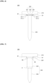
FIG. 4 is a view for describing the feed pin according to the embodiment of the present disclosure. -
FIGS. 5 to 7 are views for describing a modified example of the feed pin according to the embodiment of the present disclosure. -
FIG. 8 is a view for describing a patch antenna including the feed pin according to the embodiment of the present disclosure. -
FIGS. 9 to 12 are views for describing the modified example of the feed pin according to the embodiment of the present disclosure. -
FIGS. 13 and14 are views for describing a soldering shape and bonding strength of a general feed pin. -
FIGS. 15 and16 are views for describing a soldering shape and bonding strength of the feed pin according to the embodiment of the present disclosure. -
FIG. 17 is a view showing a fragment of the patch antenna to which the feed pin according to the embodiment of the present disclosure is applied after an electrical reliability test (i.e., an electrical thermal impact test). - Hereinafter, exemplary embodiments according to the present disclosure will be described in detail with reference to the accompanying drawings.
- The embodiments are provided to more completely describe the present disclosure to those skilled in the art, and the following embodiments may be modified in various different forms, and the scope of the present disclosure is limited to the following embodiments. Rather, the embodiments are provided to make the disclosure more faithful and complete and fully convey the spirit of the present disclosure.
- Terms used herein are intended to describe specific embodiments and are not intended to limit the present disclosure. In addition, in the present specification, singular forms may include plural forms unless the context clearly indicates otherwise.
- In the description of the embodiment, when each layer (film), area, pattern, or structure is described as being formed "on" or "under" a substrate, each layer (film), area, pad, or patterns, "on" and "under" include both cases of being formed "directly" or "indirectly with other elements interposed therebetween." In addition, in principle, the reference for "above" or "under" each layer are based on the drawing.
- The drawings are only intended to help understanding of the spirit of the present disclosure and should not be construed as limiting the scope of the present disclosure by the drawings. In addition, in the drawings, a relative thickness and length, or a relative size may be exaggerated for convenience and clarity of description.
- Referring to
FIG. 1 , ageneral patch antenna 100 includes abase substrate 110, anupper patch 120 disposed above thebase substrate 110, alower patch 130 disposed under thebase substrate 110, and afeed pin 140 for feeding theupper patch 120. - The
base substrate 110 is made of a dielectric or a magnetic material that has a dielectric constant. Thebase substrate 110 may be formed as a dielectric substrate made of ceramic with characteristics, such as a high dielectric constant and a low thermal expansion coefficient. Thebase substrate 110 may be formed as a magnetic substrate made of a magnetic material such as ferrite. - In this case, a first through
hole 112 through which thefeed pin 140 passes is formed in thebase substrate 110, and the first throughhole 112 is formed to pass through thebase substrate 110 from the top to the bottom. - The
upper patch 120 is disposed above thebase substrate 110. Theupper patch 120 is formed of a thin plate made of a conductive material with high electrical conductivity, such as copper, aluminum, gold, or silver. - In this case, a second through
hole 122 through which thefeed pin 140 passes is formed in theupper patch 120, and the second throughhole 122 is formed to pass through theupper patch 120 from the top to the bottom. The second throughhole 122 overlaps the first throughhole 112 as theupper patch 120 is fixedly disposed above thebase substrate 110. - The
upper patch 120 is fed through thefeed pin 140 to operate as a radiator for receiving GPS signals, GLONASS signals, and the like. - The
lower patch 130 is disposed on a lower surface of thebase substrate 110. In other words, thelower patch 130 is formed of a thin plate made of a conductive material with high electrical conductivity, such as copper, aluminum, gold, or silver. Thelower patch 130 is formed to have a smaller area than the lower surface of thebase substrate 110 and formed to have a larger area than theupper patch 120. In this case, thelower patch 130 needs to secure a predetermined area or more to form a ground and may be formed on the entirety of the lower surface of the dielectric to secure the area. - In this case, a third through
hole 132 through which thefeed pin 140 passes is formed in thelower patch 130, and the third throughhole 132 is formed to pass through theupper patch 120 from the top to the bottom. The third throughhole 132 overlaps the first throughhole 112 and the second throughhole 122 as theupper patch 120 is fixedly disposed under thebase substrate 110. - As the
base substrate 110, theupper patch 120, and thelower patch 130 are laminated, the first throughhole 112, the second throughhole 122, and the third throughhole 132 are aligned to form a through path through which thefeed pin 140 passes. - The
feed pin 140 includes afeed bar 142 and afeed head 144 connected to a first end portion of thefeed bar 142. A second end portion of thefeed bar 142 of thefeed pin 140 sequentially passes through theupper patch 120, thebase substrate 110, and thelower patch 130. Therefore, thefeed bar 142 is disposed in the through path, and thefeed head 144 is disposed on an upper surface of theupper patch 120. - Referring to
FIG. 2 , theconventional feed pin 140 is attached to thepatch antenna 100 through soldering. In this case, a soldering layer is formed along a side surface of thefeed head 144, and thesoldering layer 150 bonds thefeed pin 140 and thepatch antenna 100. Of course, thesoldering layer 150 may also be formed above thefeed head 144. - Referring to
FIG. 3 , in theconventional feed pin 140, the corrosion phenomenon occurs due to the reaction of lead and oxygen in thesoldering layer 150 as high and low temperatures are repeated upon an electrical reliability test (i.e., an electrical thermal impact test) of thepatch antenna 100. - In addition, micro cracks easily occur in the
conventional feed pin 140 even with a small amount of stress (impact) due to the corrosion phenomenon of thesoldering layer 150, and the characteristics of thepatch antenna 100 are changed by the micro cracks, thereby degrading reliability. - Therefore, the feed pin (hereinafter referred to as "feed pin") according to the embodiment of the present disclosure forms a first step between the feed head and the feed bar. The feed pin increases a contact area between the feed head and the
soldering layer 150 by forming the first step, thereby increasing the bonding strength. - The feed pin according to the embodiment of the present disclosure may increase the bonding strength compared to the conventional feed pin, thereby maintaining a bonding strength at a predetermined level even in the electrical reliability test in which high and low temperatures are repeated.
- In addition, compared to the conventional feed pin, the feed pin according to the embodiment of the present disclosure can maintain the bonding strength at the predetermined strength or more even in the electrical reliability test, thereby preventing the occurrence of the corrosion phenomenon and micro cracks in the
soldering layer 150 during the electrical reliability test. - Referring to
FIG. 4 , thefeed pin 200 according to the embodiment of the present disclosure includes afeed head 210, a steppedplate 220, and afeed bar 230. Hereinafter, to easily describe the embodiment of the present disclosure, thefeed bar 230, thehead 210, and the steppedplate 220 are described separately, but are not limited thereto and may be formed integrally. - The
feed head 210 is made of a conductive material. Thefeed head 210 is made of a plate-shaped conductive material. For example, thefeed head 210 is formed in a plate shape having an upper surface, a lower surface, and one or more side surfaces. In this case, thefeed head 210 is formed to have a thickness (height) of about 2 mm or more and 2.5 mm or less. - A lower surface of the
feed head 210 may be formed in a polygonal, circular, elliptical shape, or the like that has a first area. An upper surface of thefeed head 210 may have the same first area as the lower surface of thefeed head 210 and may be formed in the same shape as the lower surface of thefeed head 210. The upper surface of thefeed head 210 may have the same first area as the lower surface of thefeed head 210 and may be formed in a different shape from the lower surface of thefeed head 210. The upper surface of thefeed head 210 may have a different area from the lower surface of thefeed head 210 and may be formed in the same shape as the lower surface of thefeed head 210. The upper surface of thefeed head 210 may have a different area from the lower surface of thefeed head 210 and may be formed in a different shape from the lower surface of thefeed head 210. - A first area connected (in contact) with the stepped
plate 220 and a second area not connected (not in contact) with the steppedplate 220 may be defined on the lower surface of thefeed head 210. The first area may be defined to include a center point of the lower surface of thefeed head 210, and the second area may be defined to surround the first area of the lower surface of thefeed head 210. - The stepped
plate 220 is made of a conductive material. For example, the steppedplate 220 is formed in a plate shape having an upper surface, a lower surface, and one or more side surfaces. In this case, the steppedplate 220 is formed to have a thickness (height) of about 0.05 mm or more and 0.5 mm or less depending on the thickness (height) of thefeed head 210. - An upper surface of the stepped
plate 220 may be formed in a polygonal, circular, elliptical shape, or the like that has the second area smaller than the first area (i.e., the lower surface of the feed head 210). A lower surface of the steppedplate 220 may have the same second area as the upper surface of the steppedplate 220 and may be formed in the same shape as the upper surface of the steppedplate 220. The lower surface of the steppedplate 220 may have the second area equal to that of the upper surface of the steppedplate 220 and may be formed in a different shape from the upper surface of the steppedplate 220. The lower surface of the steppedplate 220 may have a different area from the upper surface of the steppedplate 220 and may be formed in the same shape as the upper surface of the steppedplate 220. The lower surface of the steppedplate 220 may have a different area from the upper surface of the steppedplate 220 and may be formed in a different shape from the upper surface of the steppedplate 220. - Meanwhile, the stepped
plate 220 may be formed by laminating the plurality of plate-shaped conductors. In this case, horizontal cross sections of the plurality of plate-shaped conductors may be formed to have different areas, and one or more steps may be formed on the side surfaces of the steppedplate 220. - Referring to
FIG. 5 , the steppedplate 220 is formed by laminating a first plate-shapedconductor 221 and a second plate-shapedconductor 222. - The first plate-shaped
conductor 221 is interposed between thefeed head 210 and the second plate-shapedconductor 222. In this case, an upper surface of the first plate-shapedconductor 221 may be formed in a polygonal, circular, elliptical shape, or the like that has a 2-1 area smaller than the first area. - The second plate-shaped
conductor 222 is interposed between the first plate-shapedconductor 221 and thefeed bar 230. In this case, an upper surface of the second plate-shapedconductor 222 may be formed in a polygonal, circular, elliptical shape, or the like that has a 2-2 area smaller than the 2-1 area. - The stepped
plate 220 is formed with a 1-1 step S 1-1 as the second plate-shapedconductor 222 is formed to have a smaller area than the first plate-shapedconductor 221. The 1-1 step S1-1 is formed along outer perimeters of side surfaces of the second plate-shapedconductor 222. - Referring to
FIG. 6 , the steppedplate 220 may be formed by laminating the first plate-shapedconductor 221, the second plate-shapedconductor 222, and the third plate-shapedconductor 223. - The first plate-shaped
conductor 221 is interposed between thefeed head 210 and the second plate-shapedconductor 222. In this case, an upper surface of the first plate-shapedconductor 221 may be formed in a polygonal, circular, elliptical shape, or the like that has a 2-1 area smaller than the first area. - The second plate-shaped
conductor 222 is interposed between the first plate-shapedconductor 221 and the third plate-shapedconductor 223. In this case, an upper surface of the second plate-shapedconductor 222 may be formed in a polygonal, circular, elliptical shape, or the like that has a 2-2 area smaller than the 2-1 area. - The third plate-shaped
conductor 223 is interposed between the second plate-shapedconductor 222 and thefeed bar 230. In this case, an upper surface of the third plate-shapedconductor 223 may be formed in a polygonal, circular, elliptical shape, or the like that has a 2-3 area smaller than the 2-2 area. - Since the stepped
plate 220 is formed by laminating the plate-shapedconductors conductor 222, and the 1-2 step S 1-2 is formed along outer perimeters of side surfaces of the third plate-shapedconductor 223. - In
FIGS. 5 and6 , although the example in which the steppedplate 220 is formed by laminating two or three plate-shaped conductors has been described, the present disclosure is not limited thereto and may be formed by laminating four or more plate-shaped conductors. In this case, three or more steps may be formed on the outer perimeter of the steppedplate 220. - The
feed bar 230 is made of a conductive material. In the drawing, thefeed bar 230 is formed as a polyhedron of which vertical length is larger than a horizontal length. As an example, thefeed bar 230 is made of a cylindrical conductive material. - The
feed bar 230 is disposed under the steppedplate 220. The first end portion of thefeed bar 230 is connected to the lower surface of the steppedplate 220. The first end portion of thefeed bar 230 is connected to the first area defined on the lower surface of the steppedplate 220. - The second end portion of the
feed bar 230 sequentially passes through theupper patch 320, thebase substrate 310, and thelower patch 330. - In this case, the second end portion of the
feed bar 230 may pass through the patch antenna 300 and then be exposed downward from the patch antenna 300. Here, as an example, the first end portion of thefeed bar 230 is an end portion located at the top in the drawing, and the second end portion of thefeed bar 230 is an end portion located at the bottom in the drawing. - Referring to
FIG. 7 , thefeed bar 230 may include afirst bar 232 and asecond bar 234 to prevent thefeed pin 200 from sagging when thefeed pin 200 is inserted into the patch antenna 300 and more firmly fixing thefeed pin 200 to the patch antenna 300. - Since the
feed pin 200 according to the embodiment of the present disclosure is formed to have a horizontal cross section of thesecond bar 234 smaller than a horizontal cross section of thefirst bar 232, it is possible to prevent thefeed pin 200 from sagging when a locking stopper A is formed inside the dielectric of the patch antenna 300 to insert thefeed pin 200 into the patch antenna 300 and more firmly fix thefeed pin 200 to the patch antenna 300. - In the drawing, the
first bar 232 is formed as a polyhedron of which vertical length is larger than a horizontal length. As an example, thefirst bar 232 is made of a cylindrical conductive material. Thefirst bar 232 is interposed between the steppedplate 220 and thesecond bar 234. The horizontal cross section of thefirst bar 232 is formed to have a fourth area. - In the drawing, the
second bar 234 is formed as a polyhedron of which vertical length is larger than a horizontal length. As an example, thesecond bar 234 is made of a cylindrical conductive material. Thesecond bar 234 is disposed under thefirst bar 232. The horizontal cross section of thesecond bar 234 is formed to have a fifth area smaller than the fourth area. - Since the
feed pin 200 according to the embodiment of the present disclosure is formed to have the upper surface of the steppedplate 220 smaller than the lower surface of thefeed head 210, a first step S1 is formed between thefeed head 210 and the steppedplate 220. The first step S1 is formed along the outer perimeters of the side surfaces of the steppedplate 220. - In this case, when the stepped
plate 220 is formed of a plurality of plate-shaped conductors, thefeed pin 200 may be formed with the first step S1 formed of a plurality of steps including one or more steps (i.e., a 1-1 step S1-1 and a 1-2 step S-2) formed on the steppedplate 220. - In addition, since the
feed pin 200 according to the embodiment of the present disclosure is formed to have a third area in which the cross section of thefeed bar 230 is smaller than the lower surface of the steppedplate 220, a second step S2 is formed between the steppedplate 220 and thefeed bar 230. The second step S2 is formed along the outer perimeters of the side surfaces of thefeed bar 230. - Referring to
FIG. 8 , the patch antenna 300 to which thefeed pin 200 according to the embodiment of the present disclosure is formed with a bonding space B surrounded by the lower surface of thefeed head 210, the outer perimeter of the steppedplate 220, and the upper surface of theupper patch 320. - The
feed pin 200 according to the embodiment of the present disclosure may be formed with the bonding space B greater than that of theconventional patch antenna 100 between the lower surface of thefeed head 210 and theupper patch 320, and in the soldering process, thesoldering layer 400 may also be formed in the bonding space B, thereby increasing the bonding strength of thefeed pin 200 compared to theconventional feed pin 140. - Referring to
FIGS. 9 and 10 , various types ofbonding protrusions 212 for increasing the bonding strength may be formed on the lower surface of thefeed head 210. Thebonding protrusion 212 is formed in the second area defined on the lower surface of thefeed head 210. - Referring to
FIG. 9 , a plurality of bondingprotrusions 212 having a triangular vertical cross section may be formed on the lower surface of thefeed head 210. For example, thebonding protrusions 212 are formed in a cone shape and are disposed in a row in the second area of the lower surface of thefeed head 210. - Referring to
FIG. 10 , a plurality of bondingprotrusions 212 having a semicircular vertical cross section may be formed on the lower surface of thefeed head 210. For example, thebonding protrusions 212 are formed in a hemispherical shape and are disposed in a row in the second area of the lower surface of thefeed head 210. - Meanwhile, referring to
FIG. 11 , various types ofbonding protrusions 212 and bonding grooves for increasing the bonding strength may be formed on the lower surface of thefeed head 210. Thebonding protrusions 212 and the bonding grooves are formed in the second area defined on the lower surface of thefeed head 210. - For example, the plurality of bonding
protrusions 212 and bonding grooves having a semicircular vertical cross section may be formed on the lower surface of thefeed head 210. Thebonding protrusions 212 and the bonding grooves are formed in a hemispherical shape and are alternately disposed in the second area of the lower surface of thefeed head 210. - As described above, the
feed pin 200 according to the embodiment of the present disclosure may be formed to have thebonding protrusions 212 and/or bonding grooves on the lower surface of thefeed head 210 to increase the contact area between thesoldering layer 400 formed in the soldering process and the lower surface of thefeed head 210, thereby increasing the bonding strength of thefeed pin 200. - Referring to
FIG. 12 , aninclined portion 214 for increasing the bonding strength may be formed on the lower surface of thefeed head 210. In this case, when theinclined portion 214 has an inclination closer to the upper surface of thefeed head 210 toward the outer perimeter of thefeed head 210, thesoldering layer 400 may not be formed between the lower surface of thefeed head 210 and theupper patch 320 in the soldering process. Therefore, theinclined portion 214 having the inclination closer to the upper surface of thefeed head 210 toward the outer perimeter of thefeed head 210 is formed. - As described above, the
feed pin 200 according to the embodiment of the present disclosure may have the step formed by interposing the steppedplate 220 between thefeed head 210 and thefeed bar 230 to increase the contact area between thesoldering layer 400 formed in the soldering process and the lower surface of thefeed head 210, thereby increasing the bonding strength compared to theconventional feed pin 140. - In addition, the
feed pin 200 according to the embodiment of the present disclosure may have the plurality of bondingprotrusions 212 and/or bonding grooves or theinclined portion 214 formed in the second area defined on the lower surface of thefeed head 210 to increase the contact area between thesoldering layer 400 formed in the soldering process and the lower surface of thefeed head 210, thereby further increasing the bonding strength compared to theconventional feed pin 140. - Cracks of the patch antenna 300 that occur during the electrical reliability test often occur between the lower surface of the
feed head 210 and the patch antenna 300 (i.e., the upper surface of the upper patch 320). To prevent the cracks of the patch antenna 300, the bonding strength needs to be increased by increasing a contact area with thesoldering layer 400 between the lower surface of thefeed head 210 and the upper surface of theupper patch 320. - Referring to
FIG. 13 , in thepatch antenna 100 to which thegeneral feed pin 140 is applied, a small bonding space is formed only at an edge portion of the lower surface of thefeed head 144. Since thepatch antenna 100 to which thegeneral feed pin 140 is applied has the small bonding space, the contact area between thesoldering layer 150 and thepatch antenna 100 is small, and thus the bonding strength is inevitably decreased. - Referring to
FIG. 14 , as a result of the electrical thermal impact test of thepatch antenna 100 to which thegeneral feed pin 140 is applied, the minimum strength is about 9 and the maximum strength is about 16. In this case, the average bonding strength is about 11.56. In this case, an electrical thermal impact test environment is repeated about 1000 times in a cycle that about +105°C is maintained for about 30 minutes and then - 40°C is maintained for about 30 minutes. - Meanwhile, referring to
FIG. 15 , since the patch antenna 300 to which thefeed pin 200 according to the embodiment of the present disclosure is applied has the first step S1 formed by thefeed head 210 and the steppedplate 220, the bonding space B surrounded by the lower surface of thefeed head 210, the outer perimeter of the steppedplate 220, and the upper surface of theupper patch 320. - In the patch antenna 300 to which the
feed pin 200 according to the embodiment of the present disclosure is applied, thesoldering layer 400 is formed in the bonding space B during the soldering process, and thus the contact area between thesoldering layer 400 and the patch antenna 300 relatively increases, and the bonding strength between the lower surface of thefeed head 210 and the patch antenna 300 is increased. - Referring to
FIG. 16 , as a result of the electrical thermal impact test of the patch antenna 300 to which thefeed pin 200 according to the embodiment of the present disclosure is applied, the minimum strength is about 13 and the maximum strength is about 20. In this case, the average bonding strength is about 18.3. In this case, an electrical thermal impact test environment is repeated about 1000 times in a cycle that about +105°C is maintained for about 30 minutes and then -40°C is maintained for about 30 minutes. - Referring to
FIG. 17 , it can be seen that the patch antenna 300 to which thefeed pin 200 according to the embodiment of the present disclosure is applied has no cracks between the lower surface of thefeed pin 200 and theupper patch 320 even after the electrical reliability test. - As described above, since the
feed pin 200 according to the embodiment of the present disclosure has the steppedplate 220 interposed between the lower surface of thefeed head 210 and the upper surface of thefeed bar 230, the patch antenna 300 to which thefeed pin 200 is applied may be formed with the bonding space B surrounded by the lower surface of thefeed head 210, the outer perimeter of the steppedplate 220, and the upper surface of theupper patch 320, thereby increasing the bonding strength of thefeed pin 200. - The above description is merely the exemplary description of the technical spirit of the present disclosure, and those skilled in the art to which the present disclosure pertains will be able to variously modify and change the present disclosure without departing from the essential characteristics of the present disclosure. Therefore, the embodiments disclosed in the present disclosure are not intended to limit the technical spirit of the present disclosure, but intended to describe the same, and the scope of the technical spirit of the present disclosure is not limited by these embodiments. The scope of the present disclosure should be construed according to the appended claims, and all technical spirits within the equivalent range should be construed as being included in the scope of the present disclosure.
Claims (16)
- A feed pin comprising:a feed head made of a plate-shaped conductive material with a first area;a stepped plate made of a plate-shaped conductive material having a second area and connected to a lower surface of the feed head; anda feed bar made of a polyhedral conductive material and connected to a lower surface of the stepped plate.
- The feed pin of claim 1, wherein the second area that is an area of a horizontal cross section of the stepped plate is formed to be smaller than the first area that is a horizontal cross section of the feed head, and
a first step is formed between the feed head and the stepped plate. - The feed pin of claim 2, wherein the first step is formed along the lower surface of the feed head and outer perimeters of side surfaces of the stepped plate.
- The feed pin of claim 1, wherein the stepped plate is formed by laminating a plurality of plate-shaped conductors formed to have different horizontal cross-sectional areas, and one or more steps are formed on side surfaces of the stepped plate.
- The feed pin of claim 4, wherein a first step formed between the feed head and the stepped plate includes two or more steps.
- The feed pin of claim 1, wherein a third area that is an area of a horizontal cross section of the feed bar is formed to be smaller than the second area that is a horizontal cross section of the stepped plate, and
a second step is formed between the stepped plate and the feed bar. - The feed pin of claim 1, wherein a first area connected to the feed bar and a second area that is an outer perimetric area of the first area are defined on the lower surface of the stepped plate, and
a plurality of bonding protrusions are formed in the second area. - The feed pin of claim 1, wherein a first area connected to the feed bar and a second area that is an outer perimetric area of the first area are defined on the lower surface of the stepped plate, and
an inclined portion having inclination closer to an upper surface of the feed head toward an outer perimeter of the feed head is formed in the second area. - The feed pin of claim 1, wherein the feed bar includes:a first bar disposed on the lower surface of the stepped plate; anda second bar disposed on a lower surface of the first bar, andthe second bar is formed to have a horizontal cross section smaller than a horizontal cross section of the first bar to form a locking stopper.
- A patch antenna comprising:a dielectric layer;an upper patch disposed on an upper surface of the dielectric layer;a lower patch disposed on a lower surface of the dielectric layer; anda feed pin passing through the upper patch, the dielectric layer, and the lower patch to feed the upper patch,wherein the feed bar includes:a feed head made of a plate-shaped conductive material with a first area;a stepped plate made of a plate-shaped conductive material having a second area and connected to a lower surface of the feed head; anda feed bar made of a polyhedral conductive material and connected to a lower surface of the stepped plate.
- The patch antenna of claim 10, wherein a bonding space surrounded by a lower surface of the feed head, an outer perimeter of the stepped plate, and an upper surface of the upper patch is defined, and a soldering layer is formed in the bonding space.
- The patch antenna of claim 10, wherein the second area that is an area of a horizontal cross section of the stepped plate is formed to be smaller than the first area that is a horizontal cross section of the feed head, and a first step is formed between the feed head and the stepped plate, and
a soldering layer is formed in a bonding space formed by the first step and an upper surface of the upper patch. - The patch antenna of claim 12, wherein a first area connected to the feed bar and a second area that is an outer perimetric area of the first area are defined on the lower surface of the stepped plate, and
a plurality of bonding protrusions are formed in the second area. - The patch antenna of claim 10, wherein a first area connected to the feed bar and a second area that is an outer perimetric area of the first area are defined on the lower surface of the stepped plate,an inclined portion having inclination closer to an upper surface of the feed head toward an outer perimeter of the feed head is formed in the second area, anda soldering layer is formed in a bonding space formed by the inclined portion and an upper surface of the upper patch.
- The patch antenna of claim 10, further comprising: a first soldering layer formed in a bonding space surrounded by a lower surface of the feed head, an outer perimeter of the stepped plate, and an upper surface of the upper patch; and
a second soldering layer formed in a bonding space formed by the upper surface of the upper patch and an outer perimeter of the feed head. - The patch antenna of claim 10, wherein the stepped plate is formed by laminating a plurality of plate-shaped conductors formed to have different horizontal cross-sectional areas, and one or more steps are formed on side surfaces of the stepped plate.
Applications Claiming Priority (2)
| Application Number | Priority Date | Filing Date | Title |
|---|---|---|---|
| KR1020210140296A KR102626731B1 (en) | 2021-10-20 | 2021-10-20 | Feed pin and patch antenna having the same |
| PCT/KR2022/015205 WO2023068617A1 (en) | 2021-10-20 | 2022-10-07 | Feed pin, and patch antenna comprising same |
Publications (2)
| Publication Number | Publication Date |
|---|---|
| EP4421989A1 true EP4421989A1 (en) | 2024-08-28 |
| EP4421989A4 EP4421989A4 (en) | 2025-02-19 |
Family
ID=86058256
Family Applications (1)
| Application Number | Title | Priority Date | Filing Date |
|---|---|---|---|
| EP22883840.5A Pending EP4421989A4 (en) | 2021-10-20 | 2022-10-07 | Feed pin, and patch antenna comprising same |
Country Status (5)
| Country | Link |
|---|---|
| US (1) | US20240413518A1 (en) |
| EP (1) | EP4421989A4 (en) |
| KR (1) | KR102626731B1 (en) |
| CN (1) | CN118176627A (en) |
| WO (1) | WO2023068617A1 (en) |
Family Cites Families (11)
| Publication number | Priority date | Publication date | Assignee | Title |
|---|---|---|---|---|
| JP3038295B2 (en) * | 1994-10-15 | 2000-05-08 | 東光株式会社 | Planar antenna |
| JP3084211B2 (en) * | 1995-06-23 | 2000-09-04 | 東光株式会社 | Planar antenna |
| JPH09260933A (en) * | 1996-03-25 | 1997-10-03 | Taiyo Yuden Co Ltd | How to attach the feeding pin of the patch antenna |
| US6257703B1 (en) * | 1996-07-31 | 2001-07-10 | Canon Kabushiki Kaisha | Ink jet recording head |
| JP2002344230A (en) * | 2001-05-11 | 2002-11-29 | Furukawa Electric Co Ltd:The | Small antenna |
| JP2002353730A (en) * | 2001-05-29 | 2002-12-06 | Kyocera Corp | Patch antenna |
| KR100464863B1 (en) * | 2001-12-20 | 2005-01-05 | 주식회사 선우커뮤니케이션 | Frequency response character control method for dielectric ceramic antenna, antenna device using the same method |
| JP2004165980A (en) * | 2002-11-13 | 2004-06-10 | Alps Electric Co Ltd | Patch antenna |
| KR101032961B1 (en) * | 2009-07-28 | 2011-05-09 | 주식회사 세미라인 | Manufacture method of LED heat dissipation board and its structure |
| KR101806188B1 (en) | 2016-08-16 | 2017-12-07 | 주식회사 아모텍 | Patch antenna module |
| KR102323000B1 (en) * | 2019-08-27 | 2021-11-09 | 주식회사 아모텍 | Multi band patch ant |
-
2021
- 2021-10-20 KR KR1020210140296A patent/KR102626731B1/en active Active
-
2022
- 2022-10-07 US US18/703,307 patent/US20240413518A1/en active Pending
- 2022-10-07 WO PCT/KR2022/015205 patent/WO2023068617A1/en not_active Ceased
- 2022-10-07 CN CN202280070560.7A patent/CN118176627A/en active Pending
- 2022-10-07 EP EP22883840.5A patent/EP4421989A4/en active Pending
Also Published As
| Publication number | Publication date |
|---|---|
| CN118176627A (en) | 2024-06-11 |
| WO2023068617A1 (en) | 2023-04-27 |
| KR102626731B1 (en) | 2024-01-18 |
| EP4421989A4 (en) | 2025-02-19 |
| US20240413518A1 (en) | 2024-12-12 |
| KR20230056356A (en) | 2023-04-27 |
Similar Documents
| Publication | Publication Date | Title |
|---|---|---|
| US12095180B2 (en) | Multi-band patch antenna | |
| US20180219281A1 (en) | Antenna device and method for manufacturing antenna device | |
| JP5296876B2 (en) | Multi-layer antenna device | |
| US7821460B2 (en) | Tunable patch antenna of planar construction | |
| US6897813B2 (en) | Combined antenna with antenna combining circularly polarized wave antenna and vertical antenna | |
| US8736031B2 (en) | Semiconductor package | |
| US20130207869A1 (en) | Side-face radiation antenna and wireless communication module | |
| US11309631B2 (en) | Stacked patch antenna | |
| US9245858B2 (en) | Semiconductor device package with integrated antenna for wireless applications | |
| US9257754B2 (en) | Integrated millimeter wave transceiver | |
| CN111697320A (en) | Antenna device, antenna module, and communication device | |
| JP7238755B2 (en) | Antenna device, antenna module, and communication device | |
| US12609452B2 (en) | Antenna device and communication module | |
| KR101779593B1 (en) | Patch antenna | |
| US9472843B2 (en) | Radio frequency grounding sheet for a phased array antenna | |
| EP4421989A1 (en) | Feed pin, and patch antenna comprising same | |
| US7741999B2 (en) | Multilayer antenna of planar construction | |
| US6727858B2 (en) | Circularly polarized wave antenna suitable for miniaturization | |
| US20240421487A1 (en) | Stacked patch antenna having spacers | |
| US12407108B2 (en) | Multi-band patch antenna | |
| KR102923556B1 (en) | Patch antenna module | |
| US20240421488A1 (en) | Patch antenna with ground well | |
| US20250266610A1 (en) | Electronic devices with sidewall antennas and methods of fabricating such devices | |
| KR102201572B1 (en) | an antenna for vehicle including a 3-D reflector for adjusting beam pattern and improving null | |
| KR20220050545A (en) | Patch antenna |
Legal Events
| Date | Code | Title | Description |
|---|---|---|---|
| STAA | Information on the status of an ep patent application or granted ep patent |
Free format text: STATUS: THE INTERNATIONAL PUBLICATION HAS BEEN MADE |
|
| PUAI | Public reference made under article 153(3) epc to a published international application that has entered the european phase |
Free format text: ORIGINAL CODE: 0009012 |
|
| STAA | Information on the status of an ep patent application or granted ep patent |
Free format text: STATUS: REQUEST FOR EXAMINATION WAS MADE |
|
| 17P | Request for examination filed |
Effective date: 20240507 |
|
| AK | Designated contracting states |
Kind code of ref document: A1 Designated state(s): AL AT BE BG CH CY CZ DE DK EE ES FI FR GB GR HR HU IE IS IT LI LT LU LV MC ME MK MT NL NO PL PT RO RS SE SI SK SM TR |
|
| REG | Reference to a national code |
Ref country code: DE Ref legal event code: R079 Free format text: PREVIOUS MAIN CLASS: H01Q0001460000 Ipc: H01Q0009040000 |
|
| DAV | Request for validation of the european patent (deleted) | ||
| DAX | Request for extension of the european patent (deleted) | ||
| A4 | Supplementary search report drawn up and despatched |
Effective date: 20250122 |
|
| RIC1 | Information provided on ipc code assigned before grant |
Ipc: H01Q 1/32 20060101ALN20250116BHEP Ipc: H01Q 9/04 20060101AFI20250116BHEP |