EP4421864A1 - Semiconductor device and manufacturing method thereof - Google Patents
Semiconductor device and manufacturing method thereof Download PDFInfo
- Publication number
- EP4421864A1 EP4421864A1 EP24157974.7A EP24157974A EP4421864A1 EP 4421864 A1 EP4421864 A1 EP 4421864A1 EP 24157974 A EP24157974 A EP 24157974A EP 4421864 A1 EP4421864 A1 EP 4421864A1
- Authority
- EP
- European Patent Office
- Prior art keywords
- electronic component
- semiconductor device
- liquid metal
- substrate
- cover
- Prior art date
- Legal status (The legal status is an assumption and is not a legal conclusion. Google has not performed a legal analysis and makes no representation as to the accuracy of the status listed.)
- Pending
Links
Images





Classifications
-
- H—ELECTRICITY
- H10—SEMICONDUCTOR DEVICES; ELECTRIC SOLID-STATE DEVICES NOT OTHERWISE PROVIDED FOR
- H10W—GENERIC PACKAGES, INTERCONNECTIONS, CONNECTORS OR OTHER CONSTRUCTIONAL DETAILS OF DEVICES COVERED BY CLASS H10
- H10W40/00—Arrangements for thermal protection or thermal control
- H10W40/20—Arrangements for cooling
- H10W40/22—Arrangements for cooling characterised by their shape, e.g. having conical or cylindrical projections
-
- H—ELECTRICITY
- H10—SEMICONDUCTOR DEVICES; ELECTRIC SOLID-STATE DEVICES NOT OTHERWISE PROVIDED FOR
- H10W—GENERIC PACKAGES, INTERCONNECTIONS, CONNECTORS OR OTHER CONSTRUCTIONAL DETAILS OF DEVICES COVERED BY CLASS H10
- H10W40/00—Arrangements for thermal protection or thermal control
- H10W40/20—Arrangements for cooling
- H10W40/25—Arrangements for cooling characterised by their materials
- H10W40/258—Metallic materials
-
- H—ELECTRICITY
- H10—SEMICONDUCTOR DEVICES; ELECTRIC SOLID-STATE DEVICES NOT OTHERWISE PROVIDED FOR
- H10W—GENERIC PACKAGES, INTERCONNECTIONS, CONNECTORS OR OTHER CONSTRUCTIONAL DETAILS OF DEVICES COVERED BY CLASS H10
- H10W40/00—Arrangements for thermal protection or thermal control
- H10W40/70—Fillings or auxiliary members in containers or in encapsulations for thermal protection or control
Definitions
- the invention relates to a semiconductor device and a manufacturing method thereof, and more particularly to a semiconductor device including a liquid metal and a manufacturing method thereof.
- Conventional semiconductor device includes a substrate and an electronic component disposed on the substrate.
- the electronic component inevitably generates heat during operation.
- how to dissipate the heat from the electronic component has become a prominent task for the industries.
- a semiconductor device in one embodiment, includes a substrate, an electronic component, a cover and a liquid metal.
- the electronic component is disposed on the substrate.
- the cover is disposed on the substrate, coves the electronic component and has a recess.
- the liquid metal is formed between the recess and the electronic component.
- a semiconductor method in another embodiment, includes the following steps: disposing an electronic component on a substrate; disposing a cover on the substrate to cover the electronic component, wherein the cover has recess; and forming a liquid metal between the recess and the electronic component.
- FIG. 1A illustrates a diagram view of a top view of a semiconductor device 100 according to an embodiment of the invention
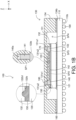
- FIG. 1B illustrates a cross-sectional view of the semiconductor device 100 of FIG. 1A along a direction 1B-1B'
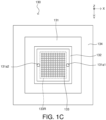
- FIG. 1C illustrates a diagram view of a bottom view of a cover 130 of FIG. 1B .
- the semiconductor device 100 is, for example, a Flip Chip Ball Grid Array (FCBGA), such as a High Performance FCBGA; however, such exemplification is not meant to be for limiting.
- FCBGA Flip Chip Ball Grid Array
- the semiconductor device 100 includes a substrate 110, an electronic component 120, a cover 130, a liquid metal 140, a first adhesive layer 150, a second adhesive layer 160, a first seal 170, a second seal 180 and at least one conductive portion 190.
- the electronic component 120 is disposed on the substrate 110.
- the cover 130 is disposed on the substrate 110 and covers the electronic component 120.
- the liquid metal 140 is formed between the cover 130 and the electronic component 120.
- the substrate 110 has, for example, single-layered structure or multilayered structure. Although not illustrated, the substrate 110 includes at least one conductive trace, at least one conductive via and /or at least one conductive pad, wherein the conductive traces are electrically connected with at least one conductive via. In an embodiment, the substrate 110 is, for example, a printed circuit board (PCB), an interposer, another semiconductor device or a semiconductor package.
- PCB printed circuit board
- the electronic component 120 is electrically connected with the conductive portion 190 through the substrate 110.
- the electronic component 120 is, for example, the component capable of applying to (or disposed on) a package requiring high-power operation, such as Flip Chip BGA (FCBGA), Fan-out package, 3D (three-dimension) IC (Integrated Circuit) package, etc.
- the electronic component 120 includes at least one conductive portion 121, wherein the conductive portion 121 is, for example, bump or solder ball.
- the electronic component 120 is bonded to the at least one conductive pad (not illustrated) of the substrate 110 through at least one conductive portion 121.
- the cover 130 is made by a material, for example, metal, such as copper, aluminum, iron or a combination thereof.
- the cover 130 could conduct heat and increased strength of the semiconductor device 100 for reducing warpage.
- the cover 130 includes a plate 131, a first surrounding portion 132, at least one pillar 133 and a second surrounding portion 134.
- the plate 131 has a first surface 131s1 and a second surface 131s2 opposite to the first surface 131s1.
- the first surface 131s1 faces the electronic component 120.
- the first surrounding portion 132, the pillars 133 and the second surrounding portion 134 are disposed on the plate 131 and protrude with respect to (or relative to) the first surface 131s1.
- the first surrounding portion 132 is, for example, a closed-ring for surrounding the whole of the liquid metal 140.
- the second surrounding portion 134 surrounds the first surrounding portion 132, the pillars 133, the electronic component 120 and the liquid metal 140.
- the second surrounding portion 134 is a closed-ring for surrounding the whole of the first surrounding portion 132, the pillars 133, the electronic component 120 and the liquid metal 140.
- the cover 130 has a first through hole 131a1 and a second through hole 131a2.
- the first through hole 131a1 and the second through hole 131a2 are located at the plate 131.
- the first through hole 131a1 and the second through hole 131a2 both extend to the second surface 131s2 from the first surface 131s1.
- the liquid metal 140 flows into through the first through hole 131a1, and air (if any) could be discharged through the second through hole 131a2.
- the first through hole 131a1 and the second through hole 131a2 are located adjacent to first surrounding portion 132.
- the first through hole 131a1 and the second through hole 131a2 are located between the whole region 133R of the pillars 133 and the first surrounding portion 132.
- the first through hole 131a1 and the second through hole 131a2 are disposed at two opposite sides of the whole region 133R or the first surrounding portion 132, and thus distance between the first through hole 131a1 and the second through hole 131a2 is long.
- the first through hole 131a1 and the second through hole 131a2 could be disposed at two opposite corners of the whole region 133R or the first surrounding portion 132 (that is, at two end of the diagonal line of the whole region 133R or the first surrounding portion 132). As a result, the distance between the first through hole 131a1 and the second through hole 131a2 is longest, and accordingly it is more conducive to exhausting the air.
- the second through hole 131a2 could be omitted, and the first through hole 131a1 could be disposed at middle position of the second surface 131s2 of the plate 131 or other position of the plate 130.
- the liquid metal 140 has melting point ranging between 60°C to 70°C, less or higher.
- the liquid metal 140 is pre-heated to be at flowable state, injected into space between the cover 130 and the electronic component 120 through the first through hole 131a1, and then solidified, without curing, by cooling or temperature drop.
- the liquid metal 140 has thermal conductivity ranging between the 70 W/m-K to 80 W/m-K, or higher.
- the thermal conductivity of the liquid metal 140 is higher than that of the thermal Interface Material (TIM).
- the TIM has thermal conductivity ranging between 2 W/m-K to 5 W/m-K.
- the liquid metal 140 is formed among the cover 130 and the electronic component 120 as a heat transfer medium. Furthermore, there are a first receiving portion SP1 formed between adjacent two pillars 133, a second receiving portion SP2 formed between a terminal 133b of each pillar 133 and the electronic component 120, and a third receiving portion SP3 formed between the first surrounding portion 132, the first surface 131s1, the outermost pillar 133 and the electronic component 120. Viewed from top of the third receiving portion SP3, the third receiving portion SP3 has a ringed-shape, for example, a closed ringed-shape.
- the liquid metal 140 includes at least one first metal portion 141, a second metal portion 142 and a third metal portion 143.
- the first metal portion 141 fills up at least portion of each first receiving portion SP1, the second metal portion 142 fills up at least portion of the second receiving portion SP2, and the third metal portion 143 fills up at least portion of the third receiving portion SP3.
- the liquid metal 140 has at least one void (or air layer) 140a, the heat generated by the electronic component 120 still could be dissipated through other heat conduction part, such as the first metal portion 141, the second metal portion 142 and the third metal portion 143 which connect the cover 130 and electronic component 120.
- FIG. 1B there is space SP4 formed among the plate 131, the first surrounding portion 132 and the second surrounding portion 134. There is no physical material formed within the space SP4, for example.
- the first adhesive layer 150 is disposed between a terminal 132b of the first surrounding portion 132 and the electronic component 120 for fixing relative position between the first surrounding portion 132 and the electronic component 120.
- the first adhesive layer 150 has a ringed-shape, for example, a closed ringed-shape for closing the gap (if any) between the first surrounding portion 132 and the electronic component 120.
- the terminal 132b has a concave 132b1 for receiving a portion of the first adhesive layer 150, and accordingly it could increase adhesion between the first surrounding portion 132 and the electronic component 120.
- the second adhesive layer 160 is disposed between a terminal 134b of the second surrounding portion 134 and the substrate 110 for fixing relative position between the cover 130 and the substrate 110.
- the second adhesive layer 160 has a ringed-shape, for example, a closed ringed-shape for closing the gap (if any) between the second surrounding portion 134 and the substrate 110.
- the first seal 170 closes or seals the first through hole 131a1.
- the liquid metal 140 is prevented from leaking through the first through hole 131a1, and an external impurity is prevented from invading an interior of the semiconductor device 100 through the first through hole 131a1.
- the second seal 180 closes the second through hole 131a2.
- the liquid metal 140 is prevented from leaking through the second through hole 131a2, and an external impurity is prevented from invading an interior of the semiconductor device 100 through the second through hole 131a2.
- the first adhesive layer 150, the second adhesive layer 160, the first seal 170 and the second seal 180 seal the receiving portions among the cover 130 and the electronic component 120 within.
- the conductive portions 190 are formed on a lower surface 110b of the substrate 110. Any one of the conductive portions 190 is, for example, bump, solder ball, etc.
- the semiconductor device 100 is bonded to and electrically connected with an external electronic device (for example, PCB, etc.) through the conductive portions 190 of the semiconductor device 100.
- FIGS. 2A to 2E illustrate manufacturing processes of the semiconductor device 100 of FIG. 1B .
- the electronic component 120 is disposed on the substrate 110, wherein the electronic component 120 includes at least one conductive portion 121, wherein the electronic component 120 is bonded to the substrate 110 through at least one conductive portion 121.
- an underfill 122 is formed between a lower surface 120b of the electronic component 120 and an upper surface 110u of the substrate 110 to encapsulate the conductive portions 121.
- the first adhesive layer 150 is formed on an upper surface 120u of the electronic component 120, wherein the first adhesive layer 150 is formed on an peripheral zone of the upper surface 120u. Viewed from top of the first adhesive layer 150, the first adhesive layer 150 has a ringed-shape, for example, a closed ringed-shape.
- the second adhesive layer 160 is formed on the upper surface 110u of the substrate 110, wherein the second adhesive layer 160 is formed on an peripheral zone of the upper surface 110u. Viewed from top of the second adhesive layer 160, the second adhesive layer 160 has a ringed-shape, for example, a closed ringed-shape.
- the embodiment of the present invention does not limit the order of forming the first adhesive layer 150 and the second adhesive layer 160.
- the cover 130 is disposed on the substrate 110 to cover the electronic component 120.
- the cover 130 includes the plate 131, the first surrounding portion 132, at least one pillar 133 and the second surrounding portion 134.
- the cover 130 has the first through hole 131a1 and the second through hole 131a2, wherein the first through hole 131a1 and the second through hole 131a2 both extend to the second surface 131s2 of the plate 131 from the first surface 131s1 of the plate 131.
- the first surrounding portion 132 of the cover 130 adheres to the electronic component 120 through the first adhesive layer 150
- the second surrounding portion 134 of the cover 130 adheres to the substrate 110 through the second adhesive layer 160 for fixing the relative position between the substrate 110 and the cover 130.
- the first adhesive layer 150 could close the gap (if any) between the first surrounding portion 132 and the electronic component 120
- the second adhesive layer 160 could close the gap (if any) between the second surrounding portion 134 and the substrate 110.
- the third receiving portion SP3 there are the first receiving portion SP1 formed between adjacent two pillars 133, the second receiving portion SP2 formed between the terminal 133b of each pillar 133 and the electronic component 120, and the third receiving portion SP3 formed between the first surrounding portion 132, the first surface 131s1, the outermost pillar 133 and the electronic component 120.
- the third receiving portion SP3 has a ringed-shape, for example, a closed ringed-shape.
- At least one conductive portion 190 is formed on the lower 110b of the substrate 110.
- the liquid metal 140 is formed between the cover 130 and the electronic component 120 by using injector 10.
- injector 10 For example, the liquid metal 140 is injected into the first receiving portion SP1, the second receiving portion SP2 and the third receiving portion SP3 through the first through hole 131a1, and gas (for example, air) A1 is discharged through the second through hole 131a2.
- gas for example, air
- the liquid metal 140 includes at least one first metal portion 141, the second metal portion 142 and the third metal portion 143.
- the first metal portion 141 fills up at least portion of each first receiving portion SP1
- the second metal portion 142 fills up at least portion of the second receiving portion SP2
- the third metal portion 143 fills up at least portion of the third receiving portion SP3.
- the heat generated by the electronic component 120 still could be dissipated through other heat conduction part, such as the first metal portion 141, the second metal portion 142 and the third metal portion 143 which connect the cover 130 and electronic component 120.
- the first seal 170 is formed within the first through hole 131a1 to seal the first through hole 131a1, as illustrated in FIG. 1B .
- the liquid metal 140 is prevented from leaking through the first through hole 131a1, and an external impurity is prevented from invading an interior of the semiconductor device 100 through the first through hole 131a1.
- the second seal 180 is formed within the second through hole 131a2 to seal the second through hole 131a2, as illustrated in FIG. 1B .
- the liquid metal 140 is prevented from leaking through the second through hole 131a2, and an external impurity is prevented from invading an interior of the semiconductor device 100 through the second through hole 131a2.
- the embodiment of the present invention does not limit the order of forming the first seal 170 and the second seal 180.
- the semiconductor device 200 includes a substrate 210, at least one electronic component 220, a cover 230, a liquid metal 240, an adhesive layer 260, a first binding promoting layer 270A and a second binding promoting layer 270B.
- the electronic component 220 is disposed on the substrate 210.
- the cover 230 is disposed on the substrate 210, covers the electronic component 220 and has a recess 230r.
- the liquid metal 240 is formed between the recess 230r and the electronic component 220. As a result, the recess 230r and the electronic component 220 could limit the flowing of the liquid metal 240 to prevent the liquid metal 240 from being overflow.
- the liquid metal 240 fills the recess 230r.
- the recess 230r may recess the liquid metal 240 for preventing the liquid metal 240 from being overflow.
- the semiconductor device 200 could be disposed on and electrically connected to the PCB 10 through at least one solder ball 211 of the substrate 210.
- the solder ball 211 may be formed on the substrate 210 during a reflow process at a temperature of about 230 °C to about 260 °C.
- the substrate 210 includes the features the same as or similar to that of the substrate 110, the electronic component 220 includes the features the same as or similar to that of the electronic component 120, and they will be not repeated here.
- the liquid metal 240 incudes a material property the same as or similar to that of the liquid metal 140, and it will not be repeated here.
- the electronic component 220 has an upper surface 220u.
- the cover 230 includes a plate 231.
- the plate 231 has a first surface 231s1 facing the electronic component 220.
- the recess 230r is recessed with respect to the first surface 231s1.
- the first surface 231s1 is lower than the upper surface 220u of the electronic component 220.
- a gap G1 (if any) between a lateral surface 230s of the recess 230r and a lateral surface 220s of the electronic component 220 could block an overflow of the liquid metal 240.
- the recess 230r has a first width W1
- the electronic component 220 has a second width W2
- the first width W1 is greater the second width W2.
- the electronic component 220 could enter the recess 230r for positioning a position between the electronic component 220 and he recess 230r, and it is conducive to the assembly of the recess 230r and the electronic component 220.
- a ratio of the first width W1 to the second width W2 could range between 1.05 and 1.10, less or greater.
- the recess 230r has a depth d1 ranging between 20 ⁇ m and 500 ⁇ m, less or greater.
- the recess 230r has a bottom surface 230b, wherein the lateral surface 230s is vertical to the bottom surface 230b.
- the lateral surface 230s is a vertical wall.
- the recess 230r could be formed by, for example, a forging process or a machining process.
- the cover 230 further includes a surrounding portion 234, wherein the surrounding portion 234 is disposed on the plate 231 and protrudes with respect to the first surface 231s1.
- the cover 230 could be formed by, for example, a forging process.
- the liquid metal 240 has melting point ranging between, for example, about 100 °C to about 200 °C, even lower or higher.
- the recess 230r could prevent the liquid metal 240 from being overflow even if the liquid metal 240 may be changed to a liquid (or fluidity) phase.
- the adhesive layer 260 is formed between the surrounding portion 234 and the substrate 210 for fixing a relative position between the substrate 210 and the cover 230.
- the adhesive layer 260 fixes relative position between the substrate 210 and the cover 230 after being cured at a temperature of about 120 °C to about 150 °C.
- the first binding promoting layers 270A could be formed between the liquid metal 240 and the cover 230 for increasing the combination of the liquid metal 240 and the cover 230
- the second binding promoting layers 270B could be formed between the liquid metal 240 and the electronic component 220 for increasing the combination of the liquid metal 240 and the electronic component 220.
- the first binding promoting layers 270A and the second binding promoting layers 270B are, for example, Au coating layer.
- FIG. 4A illustrates a diagram view of a top view of a semiconductor device 300 according to an embodiment of the invention
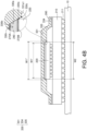
- FIG. 4B illustrates a cross-sectional view of the semiconductor device 300 of FIG. 4A along a direction 4B-4B'.
- the semiconductor device 300 includes the substrate 210, at least one electronic component 220, a cover 330, the liquid metal 240, the adhesive layer 260, the first binding promoting layer 270A and the second binding promoting layer 270B.
- the electronic component 220 is disposed on the substrate 210.
- the cover 330 is disposed on the substrate 210, covers the electronic component 220 and has a recess 330r.
- the liquid metal 240 is formed between the recess 330r and the electronic component 220. As a result, the recess 330r could limit the flowing of the liquid metal 240 to prevent the liquid metal 240 from being overflow.
- the recess 330r could be formed by, for example, a stamping process or a machining process.
- the cover 330 includes a plate 331, a surrounding portion 334 and a connection portion 335, wherein the connection portion 335 connects the plate 331 with the surrounding portion 334.
- the adhesive layer 260 is formed between the surrounding portion 334 and the substrate 210.
- the connection portion 335 is obliquely connected to the plate 331 and/or the surrounding portion 334.
- the cover 330 could be formed by, for example, a stamping process.
- the recess 330r has a bottom surface 330b and a lateral surface 330s, and the lateral surface 330s is inclined relative to the bottom surface 330b. Furthermore, the recess 330r has a plurality of first widths, the electronic component 220 has a second width, one of the first widths is smaller than the second width, and another of the first widths is greater than the second width.
- the bottom surface 330b has a first width W1'
- an opening of the recess 330r has a first width W1", wherein the first width W1' is smaller the second width W2, and the first width W1" is greater than the second width W2.
- the electronic component 220 has at least one corner 220c, and the corner 220c is in contact with the lateral surface 330s.
- the corner 220c of the electronic component 220 could is in contact with a corner 330c of a first surface 331s1 of the cover 330 and the lateral surface 330s.
- the recess 330r and the electronic component 220 could limit the flowing of the liquid metal 240 to prevent the liquid metal 240 from being overflow.
- FIGS. 5A to 5D illustrate manufacturing processes of the semiconductor device 200 of FIG. 3A .
- the substrate 210 is provided.
- At least one electronic component 220 is disposed on the substrate 210 through at least one conductive portion 221.
- the second binding promoting layer 270B could be pre-formed on the electronic component 220.
- the liquid metal 240 is formed on the electronic component 220 through the second binding promoting layer 270B.
- the cover 230 is disposed on the substrate 210 and covers the electronic component 220.
- the cover 230 has the recess 230r.
- the recess 230r is recessed with respect to the first surface 231s1 of the cover 230, and the first surface 231s1 is lower than the upper surface 220u of the electronic component 220.
- a gap G1 (if any) between a lateral surface 230s of the recess 230r and a lateral surface 220s of the electronic component 220 could block an overflow of the liquid metal 240.
- the first binding promoting layer 270A could be pre-formed on the cover 230.
- the first binding promoting layer 270A is pre-formed on the bottom surface 230b of the recess 230r.
- the cover 230 is disposed on the substrate 210 and covers the electronic component 220, wherein the liquid metal 240 is formed between the cover 230 and the electronic component 220 or fills space between the cover 230 and the electronic component 220.
- the cover 230 and the substrate 210 are connected through the adhesive layer 260.
- the adhesive layer 260 could be cured at a temperature of about 120 °C to about 150 °C. Due to the liquid metal 240 being restricted in the recess 230r, the liquid metal 240 is prevented from being flowing out of the gap G1, flowing to the substrate 210 or the lateral surface 220s of the electronic component 220 near the substrate 210 during curing process for the adhesive layer 260.
- the structure in FIG. 5C is inverted to make a bottom surface 210b face upward.
- at least one solder ball 211 is formed on the bottom surface 210b and cured through the reflow process. Due to the liquid metal 240 being restricted in the recess 230r, the liquid metal 240 is prevented from being flowing out of the gap G1, flowing to the substrate 210 or the lateral surface 220s of electronic component 220 near the substrate 210 during reflow process for the solder ball 211. Then, the substrate 210 may be disposed on the PCB 10 through the solder ball 211.
- FIGS. 6A to 6B illustrate manufacturing processes of the semiconductor device 300 of FIG. 4A .
- the substrate 210 is provided. Then, at least one electronic component 220 is disposed on the substrate 210 through at least one conductive portion 221.
- the second binding promoting layer 270B could be pre-formed on the electronic component 220.
- the liquid metal 240 is formed on the electronic component 220 through the second binding promoting layer 270B.
- the first binding promoting layer 270A could be pre-formed on the cover 330.
- the first binding promoting layer 270A is pre-formed on the bottom surface 330b of the recess 330r.
- the cover 330 is disposed on the substrate 210 and covers the electronic component 220, wherein the liquid metal 240 is formed between the cover 330 and the electronic component 220 or fills space between the cover 330 and the electronic component 220.
- the cover 330 and the substrate 210 are connected through the adhesive layer 260. Then, the adhesive layer 260 could be cured at a temperature of 120 °C to 150 °C. Due to the liquid metal 240 being restricted in the recess 330r, the liquid metal 240 is prevented from being flowing to the substrate 210 or the lateral surface 220s of the electronic component 220 near the substrate 210 during curing process for the adhesive layer 260.
- the structure in FIG. 6A is inverted to make the bottom surface 210b face upward. Then, at least one solder ball 211 is formed on the bottom surface 210b and cured through the reflow process. Due to the liquid metal 240 being restricted in the recess 330r, the liquid metal 240 is prevented from being flowing to the substrate 210 or the lateral surface of the electronic component 220 near the substrate 210 during reflow process for the solder ball 211.
Landscapes
- Structures Or Materials For Encapsulating Or Coating Semiconductor Devices Or Solid State Devices (AREA)
Abstract
A semiconductor device includes a substrate, an electronic component, a cover and a liquid metal. The electronic component is disposed on the substrate. The cover is disposed on the substrate, coves the electronic component and has a recess. The liquid metal is formed between the recess and the electronic component.
Description
- The invention relates to a semiconductor device and a manufacturing method thereof, and more particularly to a semiconductor device including a liquid metal and a manufacturing method thereof.
- Conventional semiconductor device includes a substrate and an electronic component disposed on the substrate. However, the electronic component inevitably generates heat during operation. Thus, how to dissipate the heat from the electronic component has become a prominent task for the industries.
- In one embodiment of the invention, a semiconductor device is provided. The semiconductor device includes a substrate, an electronic component, a cover and a liquid metal. The electronic component is disposed on the substrate. The cover is disposed on the substrate, coves the electronic component and has a recess. The liquid metal is formed between the recess and the electronic component.
- In another embodiment of the invention, a semiconductor method is provided. The manufacturing method includes the following steps: disposing an electronic component on a substrate; disposing a cover on the substrate to cover the electronic component, wherein the cover has recess; and forming a liquid metal between the recess and the electronic component.
- Numerous objects, features and advantages of the invention will be readily apparent upon a reading of the following detailed description of embodiments of the invention when taken in conjunction with the accompanying drawings. However, the drawings employed herein are for the purpose of descriptions and should not be regarded as limiting.
- The above objects and advantages of the invention will become more readily apparent to those ordinarily skilled in the art after reviewing the following detailed description and accompanying drawings, in which:
-
FIG. 1A illustrates a diagram view of a top view of a semiconductor device according to an embodiment of the invention; -
FIG. 1B illustrates a cross-sectional views of the semiconductor device ofFIG. 1A along a direction 1B-1B'; -
FIG. 1C illustrates a diagram view of a bottom view of a cover ofFIG. 1B ; -
FIGS. 2A to 2E illustrate manufacturing processes of the semiconductor device ofFIG. 1B ; -
FIG. 3A illustrates a diagram view of a top view of a semiconductor device disposed on a PCB according to an embodiment of the invention; -
FIG. 3B illustrates a cross-sectional view of the semiconductor device ofFIG. 3A along adirection 3B-3B'; -
FIG. 4A illustrates a diagram view of a top view of a semiconductor device according to an embodiment of the invention; -
FIG. 4B illustrates a cross-sectional view of the semiconductor device ofFIG. 4A along adirection 4B-4B'; -
FIGS. 5A to 5D illustrate manufacturing processes of the semiconductor device ofFIG. 3A ; and -
FIGS. 6A to 6B illustrate manufacturing processes of the semiconductor device ofFIG. 4A . - Referring to
FIGS. 1A to 1C ,FIG. 1A illustrates a diagram view of a top view of asemiconductor device 100 according to an embodiment of the invention,FIG. 1B illustrates a cross-sectional view of thesemiconductor device 100 ofFIG. 1A along a direction 1B-1B', andFIG. 1C illustrates a diagram view of a bottom view of acover 130 ofFIG. 1B . - The
semiconductor device 100 is, for example, a Flip Chip Ball Grid Array (FCBGA), such as a High Performance FCBGA; however, such exemplification is not meant to be for limiting. - As illustrated in
FIGS. 1A and1B , thesemiconductor device 100 includes asubstrate 110, anelectronic component 120, acover 130, aliquid metal 140, a firstadhesive layer 150, a secondadhesive layer 160, afirst seal 170, asecond seal 180 and at least oneconductive portion 190. - As illustrated in
FIG. 1B , theelectronic component 120 is disposed on thesubstrate 110. Thecover 130 is disposed on thesubstrate 110 and covers theelectronic component 120. Theliquid metal 140 is formed between thecover 130 and theelectronic component 120. As a result, the heat generated by theelectronic component 120 could be dissipated through theliquid metal 140 and thecover 130. - The
substrate 110 has, for example, single-layered structure or multilayered structure. Although not illustrated, thesubstrate 110 includes at least one conductive trace, at least one conductive via and /or at least one conductive pad, wherein the conductive traces are electrically connected with at least one conductive via. In an embodiment, thesubstrate 110 is, for example, a printed circuit board (PCB), an interposer, another semiconductor device or a semiconductor package. - The
electronic component 120 is electrically connected with theconductive portion 190 through thesubstrate 110. Theelectronic component 120 is, for example, the component capable of applying to (or disposed on) a package requiring high-power operation, such as Flip Chip BGA (FCBGA), Fan-out package, 3D (three-dimension) IC (Integrated Circuit) package, etc. Theelectronic component 120 includes at least oneconductive portion 121, wherein theconductive portion 121 is, for example, bump or solder ball. Theelectronic component 120 is bonded to the at least one conductive pad (not illustrated) of thesubstrate 110 through at least oneconductive portion 121. - The
cover 130 is made by a material, for example, metal, such as copper, aluminum, iron or a combination thereof. Thecover 130 could conduct heat and increased strength of thesemiconductor device 100 for reducing warpage. - As illustrated in
FIGS. 1B and1C , thecover 130 includes aplate 131, a first surroundingportion 132, at least onepillar 133 and a second surroundingportion 134. Theplate 131 has a first surface 131s1 and a second surface 131s2 opposite to the first surface 131s1. The first surface 131s1 faces theelectronic component 120. The first surroundingportion 132, thepillars 133 and the second surroundingportion 134 are disposed on theplate 131 and protrude with respect to (or relative to) the first surface 131s1. The first surroundingportion 132 is, for example, a closed-ring for surrounding the whole of theliquid metal 140. Since thepillars 133 protrude with respect to the first surface 131s1, and accordingly it could increase heat conduction area of thecover 130. The secondsurrounding portion 134 surrounds the first surroundingportion 132, thepillars 133, theelectronic component 120 and theliquid metal 140. The secondsurrounding portion 134 is a closed-ring for surrounding the whole of the first surroundingportion 132, thepillars 133, theelectronic component 120 and theliquid metal 140. - As illustrated in
FIGS. 1A to 1C , thecover 130 has a first through hole 131a1 and a second through hole 131a2. In the present embodiment, the first through hole 131a1 and the second through hole 131a2 are located at theplate 131. For example, the first through hole 131a1 and the second through hole 131a2 both extend to the second surface 131s2 from the first surface 131s1. As a result, during injection of theliquid metal 140, theliquid metal 140 flows into through the first through hole 131a1, and air (if any) could be discharged through the second through hole 131a2. - As illustrated in
FIGS. 1A to 1C , the first through hole 131a1 and the second through hole 131a2 are located adjacent to first surroundingportion 132. The first through hole 131a1 and the second through hole 131a2 are located between thewhole region 133R of thepillars 133 and the first surroundingportion 132. In the present embodiment, the first through hole 131a1 and the second through hole 131a2 are disposed at two opposite sides of thewhole region 133R or the first surroundingportion 132, and thus distance between the first through hole 131a1 and the second through hole 131a2 is long. As a result, during injection of theliquid metal 140, theliquid metal 140 flows into through the first through hole 131a1, and most air could be discharged through the second through hole 131a2. In another embodiment, the first through hole 131a1 and the second through hole 131a2 could be disposed at two opposite corners of thewhole region 133R or the first surrounding portion 132 (that is, at two end of the diagonal line of thewhole region 133R or the first surrounding portion 132). As a result, the distance between the first through hole 131a1 and the second through hole 131a2 is longest, and accordingly it is more conducive to exhausting the air. In another embodiment, the second through hole 131a2 could be omitted, and the first through hole 131a1 could be disposed at middle position of the second surface 131s2 of theplate 131 or other position of theplate 130. - In terms of the property, the
liquid metal 140 has melting point ranging between 60°C to 70°C, less or higher. During injection of theliquid metal 140, theliquid metal 140 is pre-heated to be at flowable state, injected into space between thecover 130 and theelectronic component 120 through the first through hole 131a1, and then solidified, without curing, by cooling or temperature drop. In addition, theliquid metal 140 has thermal conductivity ranging between the 70 W/m-K to 80 W/m-K, or higher. The thermal conductivity of theliquid metal 140 is higher than that of the thermal Interface Material (TIM). Generally, the TIM has thermal conductivity ranging between 2 W/m-K to 5 W/m-K. - As illustrated in
FIG. 1B , theliquid metal 140 is formed among thecover 130 and theelectronic component 120 as a heat transfer medium. Furthermore, there are a first receiving portion SP1 formed between adjacent twopillars 133, a second receiving portion SP2 formed between a terminal 133b of eachpillar 133 and theelectronic component 120, and a third receiving portion SP3 formed between the first surroundingportion 132, the first surface 131s1, theoutermost pillar 133 and theelectronic component 120. Viewed from top of the third receiving portion SP3, the third receiving portion SP3 has a ringed-shape, for example, a closed ringed-shape. Theliquid metal 140 includes at least onefirst metal portion 141, asecond metal portion 142 and athird metal portion 143. Thefirst metal portion 141 fills up at least portion of each first receiving portion SP1, thesecond metal portion 142 fills up at least portion of the second receiving portion SP2, and thethird metal portion 143 fills up at least portion of the third receiving portion SP3. As a result, even if theliquid metal 140 has at least one void (or air layer) 140a, the heat generated by theelectronic component 120 still could be dissipated through other heat conduction part, such as thefirst metal portion 141, thesecond metal portion 142 and thethird metal portion 143 which connect thecover 130 andelectronic component 120. - In addition, as illustrated in
FIG. 1B , there is space SP4 formed among theplate 131, the first surroundingportion 132 and the second surroundingportion 134. There is no physical material formed within the space SP4, for example. - As illustrated in
FIG. 1B , the firstadhesive layer 150 is disposed between a terminal 132b of the first surroundingportion 132 and theelectronic component 120 for fixing relative position between the first surroundingportion 132 and theelectronic component 120. In an embodiment, viewed from top of the firstadhesive layer 150, the firstadhesive layer 150 has a ringed-shape, for example, a closed ringed-shape for closing the gap (if any) between the first surroundingportion 132 and theelectronic component 120. As a result, theliquid metal 140 could be prevented from leaking through the first surroundingportion 132 and theelectronic component 120. In addition, the terminal 132b has a concave 132b1 for receiving a portion of the firstadhesive layer 150, and accordingly it could increase adhesion between the first surroundingportion 132 and theelectronic component 120. - As illustrated in
FIG. 1B , the secondadhesive layer 160 is disposed between a terminal 134b of the second surroundingportion 134 and thesubstrate 110 for fixing relative position between thecover 130 and thesubstrate 110. In an embodiment, viewed from top of the secondadhesive layer 160, the secondadhesive layer 160 has a ringed-shape, for example, a closed ringed-shape for closing the gap (if any) between the second surroundingportion 134 and thesubstrate 110. As a result, an external impurity is prevented from invading interior of thesemiconductor device 100 through the second surroundingportion 134 and thesubstrate 110. - As illustrated in
FIG. 1B , thefirst seal 170 closes or seals the first through hole 131a1. As a result, theliquid metal 140 is prevented from leaking through the first through hole 131a1, and an external impurity is prevented from invading an interior of thesemiconductor device 100 through the first through hole 131a1. In addition, there is space between thefirst seal 170 and thethird metal portion 143 of theliquid metal 140, and there is no physical material formed within the space, and thus the space could receive the thermal expansion of thethird metal portion 143. - As illustrated in
FIG. 1B , thesecond seal 180 closes the second through hole 131a2. As a result, theliquid metal 140 is prevented from leaking through the second through hole 131a2, and an external impurity is prevented from invading an interior of thesemiconductor device 100 through the second through hole 131a2. In addition, there is space between thesecond seal 180 and thethird metal portion 143 of theliquid metal 140, and there is no physical material formed within the space, and thus the space could receive the thermal expansion of thethird metal portion 143. - As illustrated in
FIG. 1B , the firstadhesive layer 150, the secondadhesive layer 160, thefirst seal 170 and thesecond seal 180 seal the receiving portions among thecover 130 and theelectronic component 120 within. - As illustrated in
FIG. 1B , theconductive portions 190 are formed on alower surface 110b of thesubstrate 110. Any one of theconductive portions 190 is, for example, bump, solder ball, etc. Thesemiconductor device 100 is bonded to and electrically connected with an external electronic device (for example, PCB, etc.) through theconductive portions 190 of thesemiconductor device 100. - Referring to
FIGS. 2A to 2E, FIGS. 2A to 2E illustrate manufacturing processes of thesemiconductor device 100 ofFIG. 1B . - As illustrated in
FIG. 2A , theelectronic component 120 is disposed on thesubstrate 110, wherein theelectronic component 120 includes at least oneconductive portion 121, wherein theelectronic component 120 is bonded to thesubstrate 110 through at least oneconductive portion 121. In addition, anunderfill 122 is formed between alower surface 120b of theelectronic component 120 and anupper surface 110u of thesubstrate 110 to encapsulate theconductive portions 121. - As illustrated in
FIG. 2B , the firstadhesive layer 150 is formed on anupper surface 120u of theelectronic component 120, wherein the firstadhesive layer 150 is formed on an peripheral zone of theupper surface 120u. Viewed from top of the firstadhesive layer 150, the firstadhesive layer 150 has a ringed-shape, for example, a closed ringed-shape. - As illustrated in
FIG. 2B , the secondadhesive layer 160 is formed on theupper surface 110u of thesubstrate 110, wherein the secondadhesive layer 160 is formed on an peripheral zone of theupper surface 110u. Viewed from top of the secondadhesive layer 160, the secondadhesive layer 160 has a ringed-shape, for example, a closed ringed-shape. - In addition, the embodiment of the present invention does not limit the order of forming the first
adhesive layer 150 and the secondadhesive layer 160. - As illustrated in
FIG. 2C , thecover 130 is disposed on thesubstrate 110 to cover theelectronic component 120. Thecover 130 includes theplate 131, the first surroundingportion 132, at least onepillar 133 and the second surroundingportion 134. Thecover 130 has the first through hole 131a1 and the second through hole 131a2, wherein the first through hole 131a1 and the second through hole 131a2 both extend to the second surface 131s2 of theplate 131 from the first surface 131s1 of theplate 131. - In
FIG. 2C , the first surroundingportion 132 of thecover 130 adheres to theelectronic component 120 through the firstadhesive layer 150, and the second surroundingportion 134 of thecover 130 adheres to thesubstrate 110 through the secondadhesive layer 160 for fixing the relative position between thesubstrate 110 and thecover 130. The firstadhesive layer 150 could close the gap (if any) between the first surroundingportion 132 and theelectronic component 120, and the secondadhesive layer 160 could close the gap (if any) between the second surroundingportion 134 and thesubstrate 110. - In
FIG. 2C , there are the first receiving portion SP1 formed between adjacent twopillars 133, the second receiving portion SP2 formed between the terminal 133b of eachpillar 133 and theelectronic component 120, and the third receiving portion SP3 formed between the first surroundingportion 132, the first surface 131s1, theoutermost pillar 133 and theelectronic component 120. Viewed from top of the third receiving portion SP3, the third receiving portion SP3 has a ringed-shape, for example, a closed ringed-shape. - As illustrated in
FIG. 2D , at least oneconductive portion 190 is formed on the lower 110b of thesubstrate 110. - As illustrated in
FIG. 2E , theliquid metal 140 is formed between thecover 130 and theelectronic component 120 by usinginjector 10. For example, theliquid metal 140 is injected into the first receiving portion SP1, the second receiving portion SP2 and the third receiving portion SP3 through the first through hole 131a1, and gas (for example, air) A1 is discharged through the second through hole 131a2. - In
FIG. 2E , theliquid metal 140 includes at least onefirst metal portion 141, thesecond metal portion 142 and thethird metal portion 143. Thefirst metal portion 141 fills up at least portion of each first receiving portion SP1, thesecond metal portion 142 fills up at least portion of the second receiving portion SP2, and thethird metal portion 143 fills up at least portion of the third receiving portion SP3. Due to many portions (for example, thefirst metal portions 141, thesecond metal portion 142 and the third metal portion 143) connecting thecover 130 andelectronic component 120, even if theliquid metal 140 has at least one void (or air layer) 140a, the heat generated by theelectronic component 120 still could be dissipated through other heat conduction part, such as thefirst metal portion 141, thesecond metal portion 142 and thethird metal portion 143 which connect thecover 130 andelectronic component 120. - Then, the
first seal 170 is formed within the first through hole 131a1 to seal the first through hole 131a1, as illustrated inFIG. 1B . As a result, theliquid metal 140 is prevented from leaking through the first through hole 131a1, and an external impurity is prevented from invading an interior of thesemiconductor device 100 through the first through hole 131a1. In addition, there is space between thefirst seal 170 and thethird metal portion 143 of theliquid metal 140, and there is no physical material formed within the space, and thus the space could receive the thermal expansion of thethird metal portion 143. - Then, the
second seal 180 is formed within the second through hole 131a2 to seal the second through hole 131a2, as illustrated inFIG. 1B . As a result, theliquid metal 140 is prevented from leaking through the second through hole 131a2, and an external impurity is prevented from invading an interior of thesemiconductor device 100 through the second through hole 131a2. In addition, there is space between thesecond seal 180 and thethird metal portion 143 of theliquid metal 140, and there is no physical material formed within the space, and thus the space could receive the thermal expansion of thethird metal portion 143. - In addition, the embodiment of the present invention does not limit the order of forming the
first seal 170 and thesecond seal 180. - Referring to
FIGS. 3A to 3B ,FIG. 3A illustrates a diagram view of a top view of asemiconductor device 200 disposed on aPCB 10 according to an embodiment of the invention, andFIG. 3B illustrates a cross-sectional view of thesemiconductor device 200 ofFIG. 3A along adirection 3B-3B'. - As illustrated in
FIGS. 3A and3B , thesemiconductor device 200 includes asubstrate 210, at least oneelectronic component 220, acover 230, aliquid metal 240, anadhesive layer 260, a first binding promotinglayer 270A and a second binding promotinglayer 270B. Theelectronic component 220 is disposed on thesubstrate 210. Thecover 230 is disposed on thesubstrate 210, covers theelectronic component 220 and has arecess 230r. Theliquid metal 240 is formed between therecess 230r and theelectronic component 220. As a result, therecess 230r and theelectronic component 220 could limit the flowing of theliquid metal 240 to prevent theliquid metal 240 from being overflow. - As illustrated in
FIG. 3B , theliquid metal 240 fills therecess 230r. As a result, therecess 230r may recess theliquid metal 240 for preventing theliquid metal 240 from being overflow. - As illustrated in
FIG. 3B , thesemiconductor device 200 could be disposed on and electrically connected to thePCB 10 through at least onesolder ball 211 of thesubstrate 210. Thesolder ball 211 may be formed on thesubstrate 210 during a reflow process at a temperature of about 230 °C to about 260 °C. - The
substrate 210 includes the features the same as or similar to that of thesubstrate 110, theelectronic component 220 includes the features the same as or similar to that of theelectronic component 120, and they will be not repeated here. In addition, theliquid metal 240 incudes a material property the same as or similar to that of theliquid metal 140, and it will not be repeated here. - As illustrated in
FIG 3B , theelectronic component 220 has anupper surface 220u. Thecover 230 includes aplate 231. Theplate 231 has a first surface 231s1 facing theelectronic component 220. Therecess 230r is recessed with respect to the first surface 231s1. The first surface 231s1 is lower than theupper surface 220u of theelectronic component 220. As a result, a gap G1 (if any) between alateral surface 230s of therecess 230r and alateral surface 220s of theelectronic component 220 could block an overflow of theliquid metal 240. In addition, the help theelectronic component 220 to easily enter therecess 230r. - As illustrated in
FIG 3B , therecess 230r has a first width W1, theelectronic component 220 has a second width W2, and the first width W1 is greater the second width W2. As a result, theelectronic component 220 could enter therecess 230r for positioning a position between theelectronic component 220 and he recess 230r, and it is conducive to the assembly of therecess 230r and theelectronic component 220. In an embodiment, a ratio of the first width W1 to the second width W2 could range between 1.05 and 1.10, less or greater. In addition, therecess 230r has a depth d1 ranging between 20 µm and 500 µm, less or greater. - As illustrated in
FIG 3B , therecess 230r has abottom surface 230b, wherein thelateral surface 230s is vertical to thebottom surface 230b. In other words, thelateral surface 230s is a vertical wall. In an embodiment, therecess 230r could be formed by, for example, a forging process or a machining process. - As illustrated in
FIG 3B , thecover 230 further includes a surroundingportion 234, wherein the surroundingportion 234 is disposed on theplate 231 and protrudes with respect to the first surface 231s1. In an embodiment, thecover 230 could be formed by, for example, a forging process. - The
liquid metal 240 has melting point ranging between, for example, about 100 °C to about 200 °C, even lower or higher. During reflow process for asolder ball 211 of thesubstrate 210 and/or curing process for theadhesive layer 260, therecess 230r could prevent theliquid metal 240 from being overflow even if theliquid metal 240 may be changed to a liquid (or fluidity) phase. - The
adhesive layer 260 is formed between the surroundingportion 234 and thesubstrate 210 for fixing a relative position between thesubstrate 210 and thecover 230. Theadhesive layer 260 fixes relative position between thesubstrate 210 and thecover 230 after being cured at a temperature of about 120 °C to about 150 °C. - As illustrated in
FIG 3B , the first binding promotinglayers 270A could be formed between theliquid metal 240 and thecover 230 for increasing the combination of theliquid metal 240 and thecover 230, and the second binding promotinglayers 270B could be formed between theliquid metal 240 and theelectronic component 220 for increasing the combination of theliquid metal 240 and theelectronic component 220. In an embodiment, the first binding promotinglayers 270A and the second binding promotinglayers 270B are, for example, Au coating layer. - Referring to
FIGS. 4A to 4B ,FIG. 4A illustrates a diagram view of a top view of asemiconductor device 300 according to an embodiment of the invention, andFIG. 4B illustrates a cross-sectional view of thesemiconductor device 300 ofFIG. 4A along adirection 4B-4B'. - As illustrated in
FIGS. 4A and4B , thesemiconductor device 300 includes thesubstrate 210, at least oneelectronic component 220, acover 330, theliquid metal 240, theadhesive layer 260, the first binding promotinglayer 270A and the second binding promotinglayer 270B. Theelectronic component 220 is disposed on thesubstrate 210. Thecover 330 is disposed on thesubstrate 210, covers theelectronic component 220 and has arecess 330r. Theliquid metal 240 is formed between therecess 330r and theelectronic component 220. As a result, therecess 330r could limit the flowing of theliquid metal 240 to prevent theliquid metal 240 from being overflow. - In an embodiment, the
recess 330r could be formed by, for example, a stamping process or a machining process. - Referring to
FIG. 4B , thecover 330 includes aplate 331, a surroundingportion 334 and aconnection portion 335, wherein theconnection portion 335 connects theplate 331 with the surroundingportion 334. Theadhesive layer 260 is formed between the surroundingportion 334 and thesubstrate 210. Theconnection portion 335 is obliquely connected to theplate 331 and/or the surroundingportion 334. In an embodiment, thecover 330 could be formed by, for example, a stamping process. - Referring to
FIG. 4B , therecess 330r has abottom surface 330b and alateral surface 330s, and thelateral surface 330s is inclined relative to thebottom surface 330b. Furthermore, therecess 330r has a plurality of first widths, theelectronic component 220 has a second width, one of the first widths is smaller than the second width, and another of the first widths is greater than the second width. For example, thebottom surface 330b has a first width W1', and an opening of therecess 330r has a first width W1", wherein the first width W1' is smaller the second width W2, and the first width W1" is greater than the second width W2. - Referring to
FIG. 4B , theelectronic component 220 has at least onecorner 220c, and thecorner 220c is in contact with thelateral surface 330s. In another embodiment, thecorner 220c of theelectronic component 220 could is in contact with acorner 330c of a first surface 331s1 of thecover 330 and thelateral surface 330s. As a result, therecess 330r and theelectronic component 220 could limit the flowing of theliquid metal 240 to prevent theliquid metal 240 from being overflow. - Referring to
FIGS. 5A to 5D, FIGS. 5A to 5D illustrate manufacturing processes of thesemiconductor device 200 ofFIG. 3A . - As illustrated in
FIG. 5A , thesubstrate 210 is provided. - As illustrated in
FIG. 5B , at least oneelectronic component 220 is disposed on thesubstrate 210 through at least oneconductive portion 221. The second binding promotinglayer 270B could be pre-formed on theelectronic component 220. Then, theliquid metal 240 is formed on theelectronic component 220 through the second binding promotinglayer 270B. - As illustrated in
FIG. 5C , thecover 230 is disposed on thesubstrate 210 and covers theelectronic component 220. Thecover 230 has therecess 230r. - In
FIG. 5C , therecess 230r is recessed with respect to the first surface 231s1 of thecover 230, and the first surface 231s1 is lower than theupper surface 220u of theelectronic component 220. As a result, a gap G1 (if any) between alateral surface 230s of therecess 230r and alateral surface 220s of theelectronic component 220 could block an overflow of theliquid metal 240. - In
FIG. 5C , the first binding promotinglayer 270A could be pre-formed on thecover 230. For example, the first binding promotinglayer 270A is pre-formed on thebottom surface 230b of therecess 230r. Then, thecover 230 is disposed on thesubstrate 210 and covers theelectronic component 220, wherein theliquid metal 240 is formed between thecover 230 and theelectronic component 220 or fills space between thecover 230 and theelectronic component 220. - . In
FIG. 5C , thecover 230 and thesubstrate 210 are connected through theadhesive layer 260. Then, theadhesive layer 260 could be cured at a temperature of about 120 °C to about 150 °C. Due to theliquid metal 240 being restricted in therecess 230r, theliquid metal 240 is prevented from being flowing out of the gap G1, flowing to thesubstrate 210 or thelateral surface 220s of theelectronic component 220 near thesubstrate 210 during curing process for theadhesive layer 260. - As illustrated in
FIG. 5D , the structure inFIG. 5C is inverted to make abottom surface 210b face upward. Then, at least onesolder ball 211 is formed on thebottom surface 210b and cured through the reflow process. Due to theliquid metal 240 being restricted in therecess 230r, theliquid metal 240 is prevented from being flowing out of the gap G1, flowing to thesubstrate 210 or thelateral surface 220s ofelectronic component 220 near thesubstrate 210 during reflow process for thesolder ball 211. Then, thesubstrate 210 may be disposed on thePCB 10 through thesolder ball 211. - Referring to
FIGS. 6A to 6B, FIGS. 6A to 6B illustrate manufacturing processes of thesemiconductor device 300 ofFIG. 4A . - As illustrated in
FIG. 6A , thesubstrate 210 is provided. Then, at least oneelectronic component 220 is disposed on thesubstrate 210 through at least oneconductive portion 221. The second binding promotinglayer 270B could be pre-formed on theelectronic component 220. Then, theliquid metal 240 is formed on theelectronic component 220 through the second binding promotinglayer 270B. The first binding promotinglayer 270A could be pre-formed on thecover 330. For example, the first binding promotinglayer 270A is pre-formed on thebottom surface 330b of therecess 330r. Then, thecover 330 is disposed on thesubstrate 210 and covers theelectronic component 220, wherein theliquid metal 240 is formed between thecover 330 and theelectronic component 220 or fills space between thecover 330 and theelectronic component 220. - As illustrated in
FIG. 6A , thecover 330 and thesubstrate 210 are connected through theadhesive layer 260. Then, theadhesive layer 260 could be cured at a temperature of 120 °C to 150 °C. Due to theliquid metal 240 being restricted in therecess 330r, theliquid metal 240 is prevented from being flowing to thesubstrate 210 or thelateral surface 220s of theelectronic component 220 near thesubstrate 210 during curing process for theadhesive layer 260. - As illustrated in
FIG. 6B , the structure inFIG. 6A is inverted to make thebottom surface 210b face upward. Then, at least onesolder ball 211 is formed on thebottom surface 210b and cured through the reflow process. Due to theliquid metal 240 being restricted in therecess 330r, theliquid metal 240 is prevented from being flowing to thesubstrate 210 or the lateral surface of theelectronic component 220 near thesubstrate 210 during reflow process for thesolder ball 211. - While the invention has been described in terms of what is presently considered to be the most practical and preferred embodiments, it is to be understood that the invention need not be limited to the disclosed embodiment. On the contrary, it is intended to cover various modifications and similar arrangements included within the scope of the appended claims which are to be accorded with the broadest interpretation so as to encompass all such modifications and similar structures.
Claims (15)
- A semiconductor device (200, 300), characterized in that the semiconductor device (200, 300) comprises:a substrate (210);an electronic component (220) disposed on the substrate (210);a cover (230, 330) disposed on the substrate (210), covering the electronic component (220) and having a recess (230r, 330r);a liquid metal (240) formed between the recess (230r, 330r) and the electronic component (220).
- The semiconductor device (200, 300) as claimed in claim 1, characterized in that the electronic component (220) has an upper surface (220u), and the cover (230, 330) comprises:a plate (231, 331) having a first surface (231s1, 331s1) facing the electronic component (220);wherein the recess (230r, 330r) is recessed with respect to the first surface (231s1, 331s1), and the first surface (231s1, 331s1) is lower than the upper surface (220u) of the electronic component (220).
- The semiconductor device (200, 300) as claimed in claim 1 or claim 2, characterized in that the recess (230r, 330r) has a first width (W1, W1'), the electronic component (220) has a second width (W2), and the first width (W1, W1') is greater the second width (W2).
- The semiconductor device (200, 300) as claimed in claim 3, characterized in that a ratio of the first width (W1, W1') to the second width (W2) ranges between 1.05 and 1.10.
- The semiconductor device (200, 300) as claimed in claim 1 or claim 2, characterized in that the recess (230r, 330r) has a plurality of first widths (W1, W1'), the electronic component (220) has a second width (W2), one of the first width (W1, W1') is smaller than the second width (W2), and another of the first widths (W1, W1') is greater than the second width (W2).
- The semiconductor device (200, 300) as claimed in claim 1, characterized in that the cover (230, 330) comprises:a plate (231, 331) having a first surface (231s1, 331s1) facing the electronic component (220);a surrounding portion (234, 334) disposed on the plate (231, 331) and protruding with respect to the first surface (231s1, 331s1);wherein the semiconductor device (200, 300) further comprises an adhesive layer (260) formed between the surrounding portion (234, 334) and the substrate (210).
- The semiconductor device (200, 300) as claimed in any one of the preceding claims, characterized in that the recess (230r, 330r) has a depth (d1) ranging between 20 µm and 500 µm.
- The semiconductor device (200, 300) as claimed in any one of the preceding claims, characterized in that the recess (230r, 330r) has a bottom surface (230b, 330b) and a lateral surface (230s, 330s), and the lateral surface (230s, 330s) is inclined relative to the bottom surface (230b, 330b).
- The semiconductor device (200, 300) as claimed in any one of claims 1 to 7, characterized in that the recess (230r, 330r) has a bottom surface (230b, 330b) and a lateral surface (230s, 330s), and the lateral surface (230s, 330s) is vertical to the bottom surface (230b, 330b).
- The semiconductor device (200, 300) as claimed in any one of claims 1 to 7, characterized in that the recess (230r, 330r) has a lateral surface (230s, 330s), the electronic component (220) has an corner, and the corner is in contact with the lateral surface (230s, 330s).
- The semiconductor device (200, 300) as claimed in any one of the preceding claims, characterized in that the liquid metal (240) has melting point ranging between 100°C to 200°C.
- A manufacturing method, comprising:disposing an electronic component (220) on a substrate (210);disposing a cover (230, 330) on the substrate (210) to cover the electronic component (220), wherein the cover has recess (230r, 330r); andforming a liquid metal (240) between the recess (230r, 330r) and the electronic component (220).
- The manufacturing method as claimed in claim 12, characterized in that the liquid metal (240) has melting point ranging between 100°C to 200°C.
- The manufacturing method as claimed in claim 12 or 13, characterized in that the manufacturing method further comprises:
forming a binding promoting layer (270A, 270B) between cover (230, 330) and the liquid metal (240). - The manufacturing method as claimed in claim 12 or 13, characterized in that the manufacturing method further comprises:
forming a binding promoting layer (270A, 270B) between the electronic component (220) and the liquid metal (240).
Applications Claiming Priority (2)
| Application Number | Priority Date | Filing Date | Title |
|---|---|---|---|
| US202363486485P | 2023-02-23 | 2023-02-23 | |
| US18/422,166 US20240170360A1 (en) | 2021-04-08 | 2024-01-25 | Semiconductor device and manufacturing method thereof |
Publications (1)
| Publication Number | Publication Date |
|---|---|
| EP4421864A1 true EP4421864A1 (en) | 2024-08-28 |
Family
ID=89977963
Family Applications (1)
| Application Number | Title | Priority Date | Filing Date |
|---|---|---|---|
| EP24157974.7A Pending EP4421864A1 (en) | 2023-02-23 | 2024-02-15 | Semiconductor device and manufacturing method thereof |
Country Status (2)
| Country | Link |
|---|---|
| EP (1) | EP4421864A1 (en) |
| TW (1) | TWI893669B (en) |
Citations (5)
| Publication number | Priority date | Publication date | Assignee | Title |
|---|---|---|---|---|
| US20190393118A1 (en) * | 2018-06-22 | 2019-12-26 | Intel Corporation | Semiconductor package with sealed thermal interface cavity with low thermal resistance liquid thermal interface material |
| US20200168523A1 (en) * | 2018-11-22 | 2020-05-28 | Siliconware Precision Industries Co., Ltd. | Electronic package, method for fabricating the same, and heat dissipator |
| US20200388554A1 (en) * | 2019-06-07 | 2020-12-10 | Intel Corporation | Lids for integrated circuit packages with solder thermal interface materials |
| EP4071799A1 (en) * | 2021-04-08 | 2022-10-12 | MediaTek Inc. | Semiconductor device and manufacturing method thereof |
| US20220375813A1 (en) * | 2021-05-24 | 2022-11-24 | Siliconware Precision Industries Co., Ltd. | Electronic package, heat dissipation structure and manufacturing method thereof |
-
2024
- 2024-02-15 EP EP24157974.7A patent/EP4421864A1/en active Pending
- 2024-02-22 TW TW113106372A patent/TWI893669B/en active
Patent Citations (5)
| Publication number | Priority date | Publication date | Assignee | Title |
|---|---|---|---|---|
| US20190393118A1 (en) * | 2018-06-22 | 2019-12-26 | Intel Corporation | Semiconductor package with sealed thermal interface cavity with low thermal resistance liquid thermal interface material |
| US20200168523A1 (en) * | 2018-11-22 | 2020-05-28 | Siliconware Precision Industries Co., Ltd. | Electronic package, method for fabricating the same, and heat dissipator |
| US20200388554A1 (en) * | 2019-06-07 | 2020-12-10 | Intel Corporation | Lids for integrated circuit packages with solder thermal interface materials |
| EP4071799A1 (en) * | 2021-04-08 | 2022-10-12 | MediaTek Inc. | Semiconductor device and manufacturing method thereof |
| US20220375813A1 (en) * | 2021-05-24 | 2022-11-24 | Siliconware Precision Industries Co., Ltd. | Electronic package, heat dissipation structure and manufacturing method thereof |
Also Published As
| Publication number | Publication date |
|---|---|
| TWI893669B (en) | 2025-08-11 |
| TW202450027A (en) | 2024-12-16 |
Similar Documents
| Publication | Publication Date | Title |
|---|---|---|
| US7996989B2 (en) | Heat dissipating device with preselected designed interface for thermal interface materials | |
| US7728440B2 (en) | Warp-suppressed semiconductor device | |
| US6969636B1 (en) | Semiconductor package with stress inhibiting intermediate mounting substrate | |
| US8106521B2 (en) | Semiconductor device mounted structure with an underfill sealing-bonding resin with voids | |
| US11610845B2 (en) | Semiconductor package and a method of fabricating the same | |
| US20200168523A1 (en) | Electronic package, method for fabricating the same, and heat dissipator | |
| CN110797321A (en) | Semiconductor package | |
| WO2011121779A1 (en) | Multichip module, printed wiring board unit, method for manufacturing multichip module, and method for manufacturing printed wiring board unit | |
| US20240321674A1 (en) | Semiconductor device | |
| EP4071799B1 (en) | Semiconductor device and manufacturing method thereof | |
| KR102228461B1 (en) | Semiconductor Package Device | |
| EP4250352A1 (en) | Semiconductor device and manufacturing method thereof | |
| US20240170360A1 (en) | Semiconductor device and manufacturing method thereof | |
| CN221102064U (en) | Packaging structure | |
| US8502083B2 (en) | Mounting substrate and electronic device | |
| TWI893669B (en) | Semiconductor device and manufacturing method thereof | |
| JP4935163B2 (en) | Semiconductor chip mounting substrate | |
| US20060118947A1 (en) | Thermal expansion compensating flip chip ball grid array package structure | |
| CN118538684A (en) | Semiconductor device and method for manufacturing the same | |
| US20230197667A1 (en) | Semiconductor device and manufacturing method thereof | |
| US20250279328A1 (en) | Chip package assembly with on-package containment system | |
| US20260018537A1 (en) | Semiconductor device and method of manufacturing the same | |
| US20260076204A1 (en) | Semiconductor package | |
| US20250210542A1 (en) | Semiconductor package | |
| JPH11121525A (en) | Semiconductor device |
Legal Events
| Date | Code | Title | Description |
|---|---|---|---|
| PUAI | Public reference made under article 153(3) epc to a published international application that has entered the european phase |
Free format text: ORIGINAL CODE: 0009012 |
|
| STAA | Information on the status of an ep patent application or granted ep patent |
Free format text: STATUS: THE APPLICATION HAS BEEN PUBLISHED |
|
| AK | Designated contracting states |
Kind code of ref document: A1 Designated state(s): AL AT BE BG CH CY CZ DE DK EE ES FI FR GB GR HR HU IE IS IT LI LT LU LV MC ME MK MT NL NO PL PT RO RS SE SI SK SM TR |
|
| STAA | Information on the status of an ep patent application or granted ep patent |
Free format text: STATUS: REQUEST FOR EXAMINATION WAS MADE |
|
| 17P | Request for examination filed |
Effective date: 20250218 |
|
| RAP3 | Party data changed (applicant data changed or rights of an application transferred) |
Owner name: MEDIATEK INC. |