EP4421559A1 - Light adjustment device and light adjustment panel - Google Patents
Light adjustment device and light adjustment panel Download PDFInfo
- Publication number
- EP4421559A1 EP4421559A1 EP22883242.4A EP22883242A EP4421559A1 EP 4421559 A1 EP4421559 A1 EP 4421559A1 EP 22883242 A EP22883242 A EP 22883242A EP 4421559 A1 EP4421559 A1 EP 4421559A1
- Authority
- EP
- European Patent Office
- Prior art keywords
- light adjustment
- terminal
- substrate
- terminal group
- end part
- Prior art date
- Legal status (The legal status is an assumption and is not a legal conclusion. Google has not performed a legal analysis and makes no representation as to the accuracy of the status listed.)
- Pending
Links
Images



Classifications
-
- G—PHYSICS
- G02—OPTICS
- G02F—OPTICAL DEVICES OR ARRANGEMENTS FOR THE CONTROL OF LIGHT BY MODIFICATION OF THE OPTICAL PROPERTIES OF THE MEDIA OF THE ELEMENTS INVOLVED THEREIN; NON-LINEAR OPTICS; FREQUENCY-CHANGING OF LIGHT; OPTICAL LOGIC ELEMENTS; OPTICAL ANALOGUE/DIGITAL CONVERTERS
- G02F1/00—Devices or arrangements for the control of the intensity, colour, phase, polarisation or direction of light arriving from an independent light source, e.g. switching, gating or modulating; Non-linear optics
- G02F1/01—Devices or arrangements for the control of the intensity, colour, phase, polarisation or direction of light arriving from an independent light source, e.g. switching, gating or modulating; Non-linear optics for the control of the intensity, phase, polarisation or colour
- G02F1/13—Devices or arrangements for the control of the intensity, colour, phase, polarisation or direction of light arriving from an independent light source, e.g. switching, gating or modulating; Non-linear optics for the control of the intensity, phase, polarisation or colour based on liquid crystals, e.g. single liquid crystal display cells
- G02F1/133—Constructional arrangements; Operation of liquid crystal cells; Circuit arrangements
- G02F1/1333—Constructional arrangements; Manufacturing methods
- G02F1/1345—Conductors connecting electrodes to cell terminals
- G02F1/13452—Conductors connecting driver circuitry and terminals of panels
-
- G—PHYSICS
- G02—OPTICS
- G02F—OPTICAL DEVICES OR ARRANGEMENTS FOR THE CONTROL OF LIGHT BY MODIFICATION OF THE OPTICAL PROPERTIES OF THE MEDIA OF THE ELEMENTS INVOLVED THEREIN; NON-LINEAR OPTICS; FREQUENCY-CHANGING OF LIGHT; OPTICAL LOGIC ELEMENTS; OPTICAL ANALOGUE/DIGITAL CONVERTERS
- G02F1/00—Devices or arrangements for the control of the intensity, colour, phase, polarisation or direction of light arriving from an independent light source, e.g. switching, gating or modulating; Non-linear optics
- G02F1/01—Devices or arrangements for the control of the intensity, colour, phase, polarisation or direction of light arriving from an independent light source, e.g. switching, gating or modulating; Non-linear optics for the control of the intensity, phase, polarisation or colour
- G02F1/13—Devices or arrangements for the control of the intensity, colour, phase, polarisation or direction of light arriving from an independent light source, e.g. switching, gating or modulating; Non-linear optics for the control of the intensity, phase, polarisation or colour based on liquid crystals, e.g. single liquid crystal display cells
- G02F1/133—Constructional arrangements; Operation of liquid crystal cells; Circuit arrangements
- G02F1/1333—Constructional arrangements; Manufacturing methods
- G02F1/133305—Flexible substrates, e.g. plastics, organic film
-
- G—PHYSICS
- G02—OPTICS
- G02F—OPTICAL DEVICES OR ARRANGEMENTS FOR THE CONTROL OF LIGHT BY MODIFICATION OF THE OPTICAL PROPERTIES OF THE MEDIA OF THE ELEMENTS INVOLVED THEREIN; NON-LINEAR OPTICS; FREQUENCY-CHANGING OF LIGHT; OPTICAL LOGIC ELEMENTS; OPTICAL ANALOGUE/DIGITAL CONVERTERS
- G02F1/00—Devices or arrangements for the control of the intensity, colour, phase, polarisation or direction of light arriving from an independent light source, e.g. switching, gating or modulating; Non-linear optics
- G02F1/01—Devices or arrangements for the control of the intensity, colour, phase, polarisation or direction of light arriving from an independent light source, e.g. switching, gating or modulating; Non-linear optics for the control of the intensity, phase, polarisation or colour
- G02F1/13—Devices or arrangements for the control of the intensity, colour, phase, polarisation or direction of light arriving from an independent light source, e.g. switching, gating or modulating; Non-linear optics for the control of the intensity, phase, polarisation or colour based on liquid crystals, e.g. single liquid crystal display cells
- G02F1/133—Constructional arrangements; Operation of liquid crystal cells; Circuit arrangements
- G02F1/1333—Constructional arrangements; Manufacturing methods
- G02F1/1345—Conductors connecting electrodes to cell terminals
-
- G—PHYSICS
- G02—OPTICS
- G02F—OPTICAL DEVICES OR ARRANGEMENTS FOR THE CONTROL OF LIGHT BY MODIFICATION OF THE OPTICAL PROPERTIES OF THE MEDIA OF THE ELEMENTS INVOLVED THEREIN; NON-LINEAR OPTICS; FREQUENCY-CHANGING OF LIGHT; OPTICAL LOGIC ELEMENTS; OPTICAL ANALOGUE/DIGITAL CONVERTERS
- G02F1/00—Devices or arrangements for the control of the intensity, colour, phase, polarisation or direction of light arriving from an independent light source, e.g. switching, gating or modulating; Non-linear optics
- G02F1/01—Devices or arrangements for the control of the intensity, colour, phase, polarisation or direction of light arriving from an independent light source, e.g. switching, gating or modulating; Non-linear optics for the control of the intensity, phase, polarisation or colour
- G02F1/13—Devices or arrangements for the control of the intensity, colour, phase, polarisation or direction of light arriving from an independent light source, e.g. switching, gating or modulating; Non-linear optics for the control of the intensity, phase, polarisation or colour based on liquid crystals, e.g. single liquid crystal display cells
- G02F1/133—Constructional arrangements; Operation of liquid crystal cells; Circuit arrangements
- G02F1/1333—Constructional arrangements; Manufacturing methods
- G02F1/1345—Conductors connecting electrodes to cell terminals
- G02F1/13458—Terminal pads
-
- G—PHYSICS
- G02—OPTICS
- G02F—OPTICAL DEVICES OR ARRANGEMENTS FOR THE CONTROL OF LIGHT BY MODIFICATION OF THE OPTICAL PROPERTIES OF THE MEDIA OF THE ELEMENTS INVOLVED THEREIN; NON-LINEAR OPTICS; FREQUENCY-CHANGING OF LIGHT; OPTICAL LOGIC ELEMENTS; OPTICAL ANALOGUE/DIGITAL CONVERTERS
- G02F1/00—Devices or arrangements for the control of the intensity, colour, phase, polarisation or direction of light arriving from an independent light source, e.g. switching, gating or modulating; Non-linear optics
- G02F1/01—Devices or arrangements for the control of the intensity, colour, phase, polarisation or direction of light arriving from an independent light source, e.g. switching, gating or modulating; Non-linear optics for the control of the intensity, phase, polarisation or colour
- G02F1/13—Devices or arrangements for the control of the intensity, colour, phase, polarisation or direction of light arriving from an independent light source, e.g. switching, gating or modulating; Non-linear optics for the control of the intensity, phase, polarisation or colour based on liquid crystals, e.g. single liquid crystal display cells
- G02F1/133—Constructional arrangements; Operation of liquid crystal cells; Circuit arrangements
- G02F1/1333—Constructional arrangements; Manufacturing methods
- G02F1/1347—Arrangement of liquid crystal layers or cells in which the final condition of one light beam is achieved by the addition of the effects of two or more layers or cells
-
- H—ELECTRICITY
- H05—ELECTRIC TECHNIQUES NOT OTHERWISE PROVIDED FOR
- H05K—PRINTED CIRCUITS; CASINGS OR CONSTRUCTIONAL DETAILS OF ELECTRIC APPARATUS; MANUFACTURE OF ASSEMBLAGES OF ELECTRICAL COMPONENTS
- H05K1/00—Printed circuits
- H05K1/02—Details
- H05K1/14—Structural association of two or more printed circuits
-
- H—ELECTRICITY
- H05—ELECTRIC TECHNIQUES NOT OTHERWISE PROVIDED FOR
- H05K—PRINTED CIRCUITS; CASINGS OR CONSTRUCTIONAL DETAILS OF ELECTRIC APPARATUS; MANUFACTURE OF ASSEMBLAGES OF ELECTRICAL COMPONENTS
- H05K1/00—Printed circuits
- H05K1/18—Printed circuits structurally associated with non-printed electric components
- H05K1/189—Printed circuits structurally associated with non-printed electric components characterised by the use of flexible or folded printed circuits
-
- H—ELECTRICITY
- H05—ELECTRIC TECHNIQUES NOT OTHERWISE PROVIDED FOR
- H05K—PRINTED CIRCUITS; CASINGS OR CONSTRUCTIONAL DETAILS OF ELECTRIC APPARATUS; MANUFACTURE OF ASSEMBLAGES OF ELECTRICAL COMPONENTS
- H05K2201/00—Indexing scheme relating to printed circuits covered by H05K1/00
- H05K2201/10—Details of components or other objects attached to or integrated in a printed circuit board
- H05K2201/10007—Types of components
- H05K2201/10128—Display
- H05K2201/10136—Liquid Crystal display [LCD]
Definitions
- the present disclosure relates to a light adjustment device and a light adjustment panel.
- a light adjustment device of Patent Literature 1 includes a light adjustment panel.
- the light adjustment panel includes a plurality of substrates and a liquid crystal layer encapsulated between the substrates. When incident light enters the light adjustment panel, the light transmittance of the incident light is adjusted in the light adjustment panel and this adjusted transmitted light is output from the light adjustment device.
- Patent Literature 1 Japanese Patent Application Laid-open Publication No. 2004-333567
- the present disclosure is made in view of the above-described problem and intended to provide a light adjustment device and a light adjustment panel with which, even when a printed circuit is coupled to a plurality of stacked light adjustment panels via flexible printed circuits, respectively, the flexible printed circuits can be coupled to the printed circuit without overlapping each other.
- a light adjustment device comprising: a panel unit in which a plurality of light adjustment panels are stacked in a first direction, each light adjustment panel including a first substrate and a second substrate, the first substrate including two or more terminal groups each including a plurality of terminals couplable to one flexible printed circuit, the second substrate overlapping the first substrate; and flexible printed circuits each coupled to one of the terminal groups of one of the light adjustment panels, wherein when the panel unit is viewed in the first direction, a plurality of the terminal groups coupled to the flexible printed circuits are provided at each of an end part of the light adjustment panel in a second direction intersecting the first direction and an end part of the light adjustment panel in a third direction opposite the second direction, and the plurality of flexible printed circuits are not superimposed on each other.
- a light adjustment panel including a first substrate and a second substrate, the first substrate including a first terminal group and a second terminal group each including a plurality of terminals couplable to one flexible printed circuit, the second substrate overlapping the first substrate, wherein the first substrate has a first side and a second side intersecting the first side, and the first terminal group is provided along the first side and the second terminal group is provided along the second side.
- FIG. 1A is a schematic diagram of a light adjustment device according to the embodiment when viewed from the upper side.
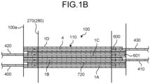
- FIG. 1B is a schematic diagram illustrating a section of FIG. 1A .
- FIG. 2 is a schematic diagram of a light adjustment panel according to the embodiment when viewed from the upper side.
- FIG. 3 is a schematic diagram of the front surface of an array substrate according to the embodiment when viewed from the upper side.
- FIG. 4 is a schematic diagram of a counter substrate according to the embodiment when turned over, illustrating its front surface on which wires are provided.
- an X direction is the right-left direction, and an X1 direction is opposite an X2 direction.
- the X1 direction is also referred to as a left direction, and the X2 direction is also referred to as a right direction.
- a Y direction is the front-back direction, and a Y1 direction is opposite a Y2 direction.
- the Y1 direction is also referred to as a front direction, and the Y2 direction is also referred to as a back direction.
- a Z direction is the up-down direction (stacking direction).
- a Z1 direction is opposite a Z2 direction.
- the Z1 direction is also referred to as an upper direction, and the Z2 direction is also referred to as a lower direction.
- the Z direction is also referred to as a first direction
- the Y1 direction is also referred to as a second direction
- the Y2 direction is also referred to as a third direction
- the X direction is also referred to as a fourth direction.
- the first direction and the second direction are orthogonal to (intersect) each other.
- the first direction and the third direction are orthogonal to (intersect) each other.
- the second direction is opposite the third direction.
- the fourth direction is orthogonal to (intersect) the first direction and the second direction.
- the fourth direction is orthogonal to (intersect) the first direction and the third direction.
- a light adjustment device 100 includes a panel unit 110 and flexible printed circuits (FPC) 400, 410, 420, and 430.
- FPC flexible printed circuits
- the shape of the panel unit 110 is a regular octagon in a plan view in the embodiment but is not limited to a regular polygon.
- the shape of the panel unit 110 according to the present invention may be a polygon the number of sides of which is four or more.
- the panel unit 110 is formed by stacking a plurality of light adjustment panels 1 in the Z direction (first direction). In the present embodiment, a plurality (in the embodiment, four) of light adjustment panels 1 illustrated in FIG. 2 are stacked.
- the four light adjustment panels 1 are a first light adjustment panel 1A, a second light adjustment panel 1B, a third light adjustment panel 1C, and a fourth light adjustment panel 1D.
- the four light adjustment panels 1 are stacked in the order of the first light adjustment panel 1A, the second light adjustment panel 1B, the third light adjustment panel 1C, and the fourth light adjustment panel 1D from the lower side.
- effective regions 270 and 280 are illustrated in FIG. 1B , and end part positions 100a positioned at the peripheries of the effective regions 270 and 280 and outside the effective regions 270 and 280 align when viewed in the stacking direction of the four light adjustment panels 1.
- the end part position 100a of the fourth light adjustment panel 1D on the left side in FIG. 1B aligns with the end part position 100a of the second light adjustment panel 1B on the left side in FIG. 1B
- the end part position 100a of the third light adjustment panel 1C on the right side in FIG. 1B aligns with the end part position 100a of the first light adjustment panel 1A on the right side in FIG. 1B
- a seal 600 is provided outside a liquid crystal layer 4, and a filler 601 is provided outside the seal 600.
- the light adjustment panels 1 vertically adjacent to each other are joined together with a translucent bonding agent 720.
- an array substrate 2 of the second light adjustment panel 1B is joined to a counter substrate 3 of the third light adjustment panel 1C with the translucent bonding agent 720 interposed therebetween.
- the light source is provided directly below the panel unit 110 when viewed in FIG. 1B .
- the flexible printed circuits 400, 410, 420, and 430 are electrically coupled to the light adjustment panels 1, respectively. As illustrated in FIG. 1A , the flexible printed circuits 400 and 420 extend in the Y1 direction, and the flexible printed circuits 410 and 430 extend in the Y2 direction. The flexible printed circuits 400, 410, 420, and 430 are not superimposed on one another when the light adjustment device 100 is viewed from the upper side. End parts of the flexible printed circuits 400, 410, 420, and 430 are each electrically coupled to a connector 510 provided on a printed circuit 500. A harness 520 is provided on the printed circuit 500. The connector 510 is electrically coupled to the harness 520.
- each light adjustment panel 1 includes the array substrate (first substrate) 2 and the counter substrate (second substrate) 3 disposed on the upper side of the array substrate 2.
- Each adjust light panel 1 is a regular octagon in a plan view and has a first side 11, a second side 12, a third side 13, a fourth side 14, a fifth side 15, a sixth side 16, a seventh side 17, and an eighth side 18.
- the first side 11 is positioned on the Y1 side on the light adjustment panel 1.
- the first side 11 extends in the X direction.
- the first side 11 of the light adjustment panel 1 overlaps a first side 211 of the array substrate 2 illustrated in FIG. 3 .
- a first side 311 of the counter substrate 3 illustrated in FIG. 4 is positioned on the Y2 side relative to the first side 211 of the array substrate 2.
- an end part 2c of the array substrate 2 on the Y1 side is exposed when the counter substrate 3 is stacked on the upper side relative to the array substrate 2.
- a first terminal group 10 is provided at the end part 2c.
- the second side 12 is positioned on the X1 side on the light adjustment panel 1.
- the second side 12 extends in the Y direction.
- the second side 12 of the light adjustment panels 1 overlaps a second side 212 of the array substrate 2 illustrated in FIG. 3 .
- a second side 312 of the counter substrate 3 illustrated in FIG. 4 is positioned on the X2 side relative to the second side 212 of the array substrate 2.
- an end part 2d of the array substrate 2 on the X1 side is exposed when the counter substrate 3 is stacked on the upper side relative to the array substrate 2.
- a second terminal group 20 is provided at the end part 2d.
- the third side 13 intersects both the X1 direction and the Y1 direction.
- the angle of the intersection is 45°.
- the third side 13 overlaps a third side 213 of the array substrate 2 illustrated in FIG. 3 and a third side 313 of the counter substrate 3 illustrated in FIG. 4 .
- the fourth side 14 intersects both the X1 direction and the Y2 direction.
- the angle of the intersection is 45°.
- the fourth side 14 overlaps a fourth side 214 of the array substrate 2 illustrated in FIG. 3 and a fourth side 314 of the counter substrate 3 illustrated in FIG. 4 .
- the fifth side 15 is positioned on the Y2 side on the light adjustment panel 1.
- the fifth side 15 overlaps a fifth side 215 of the array substrate 2 illustrated in FIG. 3 and a fifth side 315 of the counter substrate 3 illustrated in FIG. 4 .
- the sixth side 16 intersects both the X2 direction and the Y2 direction.
- the angle of the intersection is 45°.
- the sixth side 164 overlaps a sixth side 216 of the array substrate 2 illustrated in FIG. 3 and a sixth side 316 of the counter substrate 3 illustrated in FIG. 4 .
- the seventh side 17 is positioned on the X2 side on the light adjustment panel 1.
- the seventh side 17 overlaps a seventh side 217 of the array substrate 2 illustrated in FIG. 3 and a seventh side 317 of the counter substrate 3 illustrated in FIG. 4 .
- the eighth side 18 intersects both the X2 direction and the Y1 direction.
- the angle of the intersection is 45°.
- the eighth side 18 overlaps an eighth side 218 of the array substrate 2 illustrated in FIG. 3 and an eighth side 318 of the counter substrate 3 illustrated in FIG. 4 .
- the area of the counter substrate 3 is smaller than the area of the array substrate 2, and thus the first terminal group 10 provided at the end part 2c of the array substrate 2 and the second terminal group 20 provided at the end part 2d of the array substrate 2 are exposed.
- the third side 13, which couples the first side 11 and the second side 12, has a straight line shape intersecting the first side 11 and the second side 12 but may have a curved line shape such as a convex circular arc shape. This is the same for the fourth side 14, the sixth side 16, and the eighth side 18.
- FIG. 4 is a schematic diagram illustrating a front surface 3a on which wires are provided among the front and back surfaces of the counter substrate 3. Accordingly, the X1 and X2 directions of the counter substrate 3 in FIG. 4 are opposite the X1 and X2 directions of the array substrate 2 in FIG. 3.
- FIG. 3 illustrates a central line CL1 extending in the Y direction through the center of the array substrate 2 in the X direction, and a central line CL2 extending in the X direction through the center of the array substrate 2 in the Y direction. As illustrated in FIG.
- the first terminal group 10 is provided at a first end part 21 (illustrated with dashed and double-dotted lines) on a side closer to the second side 212 (or the third side 213) with respect to the center of the first side 211.
- the end part 2c is an end part of the array substrate 2 on the Y1 side
- the first end part 21 illustrated with dashed and double-dotted lines is disposed on the X1 side of the central line CL1 among sites of the end part 2c.
- the first terminal group 10 is provided at the first end part 21. As illustrated in FIG.
- the first terminal group 10 includes a first terminal 101, a second terminal 102, a third terminal 103, and a fourth terminal 104.
- the first terminal 101, the second terminal 102, the third terminal 103, and the fourth terminal 104 are sequentially arranged in the X direction (fourth direction) from the X1 side toward the X2 side.
- the terminals 101 to 104 each have a pair of short sides 105 parallel to the first side 211 and a pair of long sides 106 parallel to the second side 212.
- the second terminal group 20 is provided at a second end part 22 (illustrated with dashed and double-dotted lines) on a side closer to the first side 211 (or the third side 213) with respect to the center of the second side 212.
- the end part 2d is an end part of the array substrate 2 on the X1 side
- the second end part 22 illustrated with dashed and double-dotted lines is disposed on the Y1 side of the central line CL2 among sites of the end part 2d.
- the second terminal group 20 is provided at the second end part 22. As illustrated in FIG.
- the second terminal group 20 includes a fifth terminal 201, a sixth terminal 202, a seventh terminal 203, and an eighth terminal 204.
- the fifth terminal 201, the sixth terminal 202, the seventh terminal 203, and the eighth terminal 204 are sequentially arranged in the front-back direction (Y direction) from the Y1 side toward the Y2 side.
- the terminals 201 to 204 each have a pair of long sides 107 parallel to the first side 211 and a pair of short sides 108 parallel to the second side 212.
- Wires on the array substrate 2 and the counter substrate 3 Wires are provided on the front surface of each substrate among the front and back surfaces thereof.
- a surface on which wires are provided is referred to as the front surface
- a surface opposite to the front surface is referred to as the back surface.
- wires, liquid crystal drive electrodes, and coupling portions are provided on a front surface 2a of the array substrate 2.
- a coupling portion C1 of the array substrate 2 and a coupling portion C3 of the counter substrate 3 are electrically coupled to each other through a conductive pillar (not illustrated) through which conduction is possible.
- a coupling portion C2 of the array substrate 2 and a coupling portion C4 of the counter substrate 3 are electrically coupled to each other through a common electrode (not illustrated) through which conduction is possible.
- the first terminal 101 and the fifth terminal 201 are electrically coupled to each other through a wire (first wire) 241.
- a bifurcation point 242 is provided halfway through the wire 241, and a wire extends from the bifurcation point 242 to the coupling portion C1.
- the second terminal 102 and the sixth terminal 202 are electrically coupled to each other through wires (second wires) 243 and 245.
- a bifurcation point 244 is provided on the wire 243, and a wire 246 extends from the bifurcation point 244 to an end 247.
- the third terminal 103 and the seventh terminal 203 are electrically coupled to each other through a wire (third wire) 248.
- the fourth terminal 104 and the eighth terminal 204 are electrically coupled to each other through wires (fourth wires) 249 and 251.
- the wire 249 extends up to a bifurcation point 250 from the fourth terminal 104 toward the X2 side.
- the wire 251 extends from the bifurcation point 250 to the eighth terminal 204.
- a wire extends from the bifurcation point 250 to the coupling portion C2.
- a plurality of liquid crystal drive electrodes 261 are coupled to the wires 243 and 246.
- the liquid crystal drive electrodes 261 extend straight in the X direction.
- the liquid crystal drive electrodes 261 are disposed at equal intervals in the Y direction.
- a plurality of liquid crystal drive electrodes 262 are coupled to the wire 248.
- the liquid crystal drive electrodes 262 extend straight in the X direction.
- the liquid crystal drive electrodes 262 are disposed at equal intervals in the Y direction.
- the liquid crystal drive electrodes 261 and 262 are alternately arranged in the Y direction.
- wires, liquid crystal drive electrodes, and coupling portions are provided on the front surface 3a of the counter substrate 3.
- the central lines CL1 and CL2 illustrated in FIG. 4 correspond to the central lines CL1 and CL2 illustrated in FIG. 3 .
- the coupling portion C3 is coupled to wires 342 and 343 through a bifurcation point 341.
- the wire 342 extends to an end 348.
- the wire 343 extends to an end 349.
- the coupling portion C4 is coupled to wires 345 and 346 through a bifurcation point 344.
- the wire 346 extends to an end 347.
- a plurality of liquid crystal drive electrodes 361 are coupled to the wires 342 and 343.
- the liquid crystal drive electrodes 361 extend straight in the Y direction.
- the liquid crystal drive electrodes 361 are disposed at equal intervals in the X direction.
- a plurality of liquid crystal drive electrodes 362 are coupled to the wire 346.
- the liquid crystal drive electrodes 362 extend straight in the Y direction.
- the liquid crystal drive electrodes 362 are disposed at equal intervals in the X direction.
- the liquid crystal drive electrodes 361 and 362 are alternately arranged in the X direction.
- FIG. 5 is a schematic diagram illustrating the effective region of the array substrate according to the embodiment.
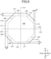
- FIG. 6 is a schematic diagram illustrating the effective region of the counter substrate according to the embodiment when turned over, illustrating the front surface 3a of the counter substrate 3 as in FIG. 4 . Accordingly, the X1 and X2 directions of the counter substrate 3 in FIG. 6 are opposite the X1 and X2 directions of the array substrate 2 in FIG. 5 .
- the effective region 270 illustrated with dashed lines is disposed at a central part of the array substrate 2.
- the effective region 270 is a regular octagon.
- the effective region 270 has a first side 271, a second side 272, a third side 273, a fourth side 274, a fifth side 275, a sixth side 276, a seventh side 277, and an eighth side 278.
- the first side 271 of the effective region 270 is disposed on the Y2 side relative to the first side 211 of the array substrate 2 and is parallel to the first side 211.
- the first side 211 and the first side 271 are separated from each other by a distance d1.
- the second side 272 of the effective region 270 is disposed on the X2 side relative to the second side 212 of the array substrate 2 and is parallel to the second side 212.
- the second side 212 and the second side 272 are separated from each other by a distance d2.
- the third side 273 of the effective region 270 is disposed on the X2 side and the Y2 side relative to the third side 213 of the array substrate 2 and is parallel to the third side 213.
- the fourth side 274 of the effective region 270 is disposed on the X2 side and the Y1 side relative to the fourth side 214 of the array substrate 2 and is parallel to the fourth side 214.
- the fifth side 275 of the effective region 270 is disposed on the Y1 side relative to the fifth side 215 of the array substrate 2 and is parallel to the fifth side 215.
- the fifth side 215 and the fifth side 275 are separated from each other by a distance d3.
- the sixth side 276 of the effective region 270 is disposed on the X1 side and the Y1 side relative to the sixth side 216 of the array substrate 2 and is parallel to the sixth side 216.
- the seventh side 277 of the effective region 270 is disposed on the X1 side relative to the seventh side 217 of the array substrate 2 and is parallel to the seventh side 217.
- the seventh side 217 and the seventh side 277 are separated from each other by a distance d4.
- the eighth side 278 of the effective region 270 is disposed on the X1 side and the Y2 side relative to the eighth side 218 of the array substrate 2 and is parallel to the eighth side 218. As illustrated in FIG. 5 , the outside of the effective region 270 is an ineffective region 279. The distances d1, d2, d3, and d4 are equal to one another.
- the effective region 280 illustrated with dashed lines is disposed at a central part of the counter substrate 3.
- the effective region 280 is a regular octagon.
- the effective region 280 includes a first side 281, a second side 282, a third side 283, a fourth side 284, a fifth side 285, a sixth side 286, a seventh side 287, and an eighth side 288.
- the first side 281 of the effective region 280 is disposed on the Y2 side relative to the first side 311 of the counter substrate 3 and is parallel to the first side 311.
- the first side 311 and the first side 281 are separated from each other by a distance d5.
- the second side 282 of the effective region 280 is disposed on the X2 side relative to the second side 312 of the counter substrate 3 and is parallel to the second side 312.
- the second side 312 and the second side 282 are separated from each other by a distance d6.
- the third side 283 of the effective region 280 is disposed on the X2 side and the Y2 side relative to the third side 313 of the counter substrate 3 and is parallel to the third side 313.
- the fourth side 284 of the effective region 280 is disposed on the X2 side and the Y1 side relative to the fourth side 314 of the counter substrate 3 and is parallel to the fourth side 314.
- the fifth side 285 of the effective region 280 is disposed on the Y1 side relative to the fifth side 315 of the counter substrate 3 and is parallel to the fifth side 315.
- the fifth side 315 and the fifth side 285 are separated from each other by a distance d7.
- the sixth side 286 of the effective region 280 is disposed on the X1 side and the Y1 side relative to the sixth side 316 of the counter substrate 3 and is parallel to the sixth side 316.
- the seventh side 287 of the effective region 280 is disposed on the X1 side relative to the seventh side 317 of the counter substrate 3 and is parallel to the seventh side 317.
- the seventh side 317 and the seventh side 287 are separated from each other by a distance d8.
- the eighth side 288 of the effective region 280 is disposed on the X1 side and the Y2 side relative to the eighth side 318 of the counter substrate 3 and is parallel to the eighth side 318.
- the outside of the effective region 280 is an ineffective region 289.
- the distances d5 and d6 are equal to each other, and the distances d7 and d8 are equal to each other.
- the distances d5 and d6 are shorter than the distances d7 and d8.
- the distances d7 and d8 are equal to the distances d1, d2, d3, and d4.
- the effective region 270 of the array substrate 2 and the effective region 280 of the counter substrate 3 have the same shape and the same size. In other words, the effective regions 270 and 280 are congruent with each other. Accordingly, the effective regions 270 and 280 match each other in a plan view when the array substrate 2 and the counter substrate 3 are stacked with their outer peripheries aligned.
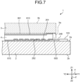
- each light adjustment panel 1 includes the array substrate (first substrate) 2, the counter substrate (second substrate) 3, and the liquid crystal layer 4.
- the counter substrate 3 is disposed on the upper side (Z1 side) of the array substrate 2.
- the liquid crystal layer 4 is provided between the counter substrate 3 and the array substrate 2. Specifically, the front surface 2a of the array substrate 2 and the front surface 3a of the counter substrate 3 face each other with the liquid crystal layer 4 interposed therebetween.
- the array substrate 2 has a back surface 2b opposite the front surface 2a, and the counter substrate 3 has a back surface 3b opposite the front surface 3a. Since the area of the counter substrate 3 is smaller than the area of the array substrate 2 as described above, the third terminal 103 provided on the front surface 2a of the array substrate 2 is exposed.
- An insulating layer, which is provided to prevent contact between two wires, is not provided in the light adjustment panel 1 according to the present embodiment because no wires on the array substrate (first substrate) 2 overlap each other.
- alignment films 610 are stacked on both substrates and the electrodes as illustrated in FIG. 7 .
- one of the alignment films 610 is stacked on the front surface 2a of the array substrate 2 and the upper surfaces of the liquid crystal drive electrodes 261 and 262, and part of the third wire 248.
- the other alignment film 610 is stacked on the front surface 3a of the counter substrate 3 and the upper surfaces of the liquid crystal drive electrodes 361.
- the array substrate 2 and the counter substrate 3 are bonded to each other by the seal 600 enclosing the effective regions, and the liquid crystal layer 4 fills a space formed by the seal 600.
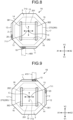
- FIG. 8 is a schematic diagram of the first light adjustment panel included in the light adjustment device in FIG. 1A when viewed from the upper side.
- FIG. 9 is a schematic diagram of the second light adjustment panel included in the light adjustment device in FIG. 1A when viewed from the upper side.
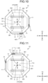
- FIG. 10 is a schematic diagram of the third light adjustment panel included in the light adjustment device in FIG. 1A when viewed from the upper side.
- FIG. 11 is a schematic diagram of the fourth light adjustment panel included in the light adjustment device in FIG. 1A when viewed from the upper side.
- the stacking order of the four light adjustment panels 1A, 1B, 1C, and 1D is not particularly limited but may be any order although the present embodiment describes a case where the first light adjustment panel 1A is disposed lowermost, the second light adjustment panel 1B is stacked on the upper side of the first light adjustment panel 1A, the third light adjustment panel 1C is stacked on the upper side of the second light adjustment panel 1B, and the fourth light adjustment panel 1D is disposed uppermost.
- a center C is illustrated at the center of each of the light adjustment panels 1A, 1B, 1C, and 1D.
- the first terminal group 10 is positioned on the Y1 side and the second terminal group 20 is positioned on the X1 side.
- the flexible printed circuit 400 is electrically coupled to the first terminal group 10 and extends toward the Y1 side.
- the second terminal group 20 on which no circuit is mounted is sealed with a moisture-proof material such as silicone.
- the effective region 270 (280) is illustrated with a regular octagon in FIGS. 8 to 11 .
- an alignment direction 710 of the alignment film 610 on the array substrate 2 is, for example, the Y direction
- an alignment direction 711 of the alignment film 610 on the counter substrate 3 is a direction orthogonal to the alignment direction 710 of the array substrate 2.
- the first terminal group 10 is positioned on the Y2 side and the second terminal group 20 is positioned on the X2 side.
- the second light adjustment panel 1B is the same as the first light adjustment panel 1A rotated by 180° in a plan view.
- the flexible printed circuit 410 is electrically coupled to the first terminal group 10 and extends toward the Y2 side.
- the second terminal group 20 on which no circuit is mounted is sealed with a moisture-proof material such as silicone.
- the alignment direction 710 of the alignment film 610 on the array substrate 2 is, for example, the Y direction
- the alignment direction 711 of the alignment film 610 on the counter substrate 3 is the direction orthogonal to the alignment direction 710 of the array substrate 2.
- the second terminal group 20 is positioned on the Y1 side and the first terminal group 10 is positioned on the X2 side.
- the third light adjustment panel 1C is the same as the first light adjustment panel 1A rotated by 90° in the anticlockwise direction in a plan view.
- the flexible printed circuit 420 is electrically coupled to the second terminal group 20 and extends toward the Y1 side.
- the first terminal group 10 on which no circuit is mounted is sealed with a moisture-proof material such as silicone.
- the alignment direction 710 of the alignment film 610 on the array substrate 2 is, for example, the X direction
- the alignment direction 711 of the alignment film 610 on the counter substrate 3 is the direction orthogonal to the alignment direction 710 of the array substrate 2.
- the fourth light adjustment panel 1D disposed uppermost, the second terminal group 20 is positioned on the Y2 side and the first terminal group 10 is positioned on the X1 side.
- the fourth light adjustment panel 1D is the same as the light adjustment panel 1A rotated by 270° in the anticlockwise direction in a plan view.
- the flexible printed circuit 430 is electrically coupled to the second terminal group 20 and extends toward the Y2 side.
- the first terminal group 10 on which no circuit is mounted is sealed with a moisture-proof material such as silicone.
- the alignment direction 710 of the alignment film 610 on the array substrate 2 is, for example, the X direction
- the alignment direction 711 of the alignment film 610 on the counter substrate 3 is the direction orthogonal to the alignment direction 710 of the array substrate 2.
- the light adjustment device 100 includes: the panel unit 110 in which a plurality of light adjustment panels 1 are stacked in the Z direction (first direction), each light adjustment panel 1 including the array substrate (first substrate) 2 and the counter substrate (second substrate) 3, the array substrate (first substrate) 2 including two or more of the first terminal group 10 and the second terminal group 20 (terminal groups) each including a plurality of terminals that can be coupled to one flexible printed circuit 400, 410, 420, or 430, the counter substrate (second substrate) 3 overlapping the array substrate 2; and the flexible printed circuits 400, 410, 420, and 430 each coupled to one of the terminal groups of one of the light adjustment panels 1.
- a plurality of the terminal groups coupled to the flexible printed circuits 400, 410, 420, and 430 are provided at each of an end part of the light adjustment panel 1 in the Y1 direction (second direction) intersecting the Z direction and an end part of the light adjustment panel 1 in the Y2 direction (third direction) opposite the Y1 direction, the plurality of flexible printed circuits 400, 410, 420, and 430 are not superimposed on each other. More specifically, the flexible printed circuit 400 of the light adjustment panel 1A and the flexible printed circuit 420 of the light adjustment panel 1C both extend in the Y1 direction.
- the first terminal group 10 of the light adjustment panel 1A, which faces the flexible printed circuit 400, and the second terminal group 20 of the light adjustment panel 1C, which faces the flexible printed circuit 420, are arranged alongside each other in the X direction in a plan view, and accordingly, the flexible printed circuits 400 and 420 are not superimposed on each other in a plan view.
- the flexible printed circuit 410 of the light adjustment panel 1B and the flexible printed circuit 430 of the light adjustment panel 1D both extend in the Y2 direction and the first terminal group 10 of the light adjustment panel 1B, which faces the flexible printed circuit 410, and the second terminal group 20 of the light adjustment panel 1D, which faces the flexible printed circuit 430, are arranged alongside each other in the X direction in a plan view, and accordingly, the flexible printed circuits 410 and 430 are not superimposed on each other in a plan view.
- the number of printed circuits increases and the size of the light adjustment device potentially increases when flexible printed circuits are extended in a plurality of directions from each light adjustment panel in a plan view in a case where the printed circuits are coupled to each of a plurality of stacked light adjustment panels via the flexible printed circuits.
- the flexible printed circuits 400, 410, 420, and 430 are extended from sides in the Y1 direction (second direction) and the Y2 direction (third direction) on each light adjustment panel 1 in a plan view.
- the number of printed circuits 500 can be reduced in a case where the printed circuits 500 are coupled in a non-superimposed state to each of a plurality of stacked light adjustment panels 1 via the flexible printed circuits 400, 410, 420, and 430.
- flexible printed circuits are extended for one printed circuit in one direction from each light adjustment panel in a plan view; however, this case is disadvantageous in that the number of flexible printed circuits that can be extended in a non-superimposed state decreases.
- only the two flexible printed circuits 400 and 420 can be extended in a case where a plurality of flexible printed circuits are extended in a non-superimposed state only in the Y1 direction as illustrated in FIG. 1A .
- the four flexible printed circuits 400, 410, 420, and 430 can be extended in the two Y1 and Y2 directions as in the present embodiment.
- the first terminal 101, the second terminal 102, the third terminal 103, and the fourth terminal 104 (terminals) included in the first terminal group 10 are electrically coupled to the fifth terminal 201, the sixth terminal 202, the seventh terminal 203, and the eighth terminal 204 (terminals) included in the second terminal group 20.
- the flexible printed circuits 400, 410, 420, and 430 can be coupled to any of the first terminal group 10 and the second terminal group 20. Accordingly, for example, in the panel unit 110 in which the four light adjustment panels 1A, 1B, 1C, and 1D are vertically stacked, the flexible printed circuits 400 and 420 extended in the Y1 direction are not superimposed on the flexible printed circuits 410 and 430 extended in the Y2 direction as illustrated in FIG. 1A by changing the orientations of the light adjustment panels 1A, 1B, 1C, and 1D.
- the first terminal group 10 and the second terminal group 20 coupled to the flexible printed circuits 400, 410, 420, and 430 are arranged in the X direction (fourth direction) intersecting the Z direction and the Y1 direction when the panel unit 110 is viewed in the Z direction.
- the first terminal groups 10 or the second terminal groups 20 coupled to the flexible printed circuits 400, 410, 420, and 430 are disposed in a non-superimposed state on the Y1 side or the Y2 side in a plan view.
- the array substrate 2 is shaped in an octagon that has the first side 211 and the second side 212 intersecting the first side 211 (in a polygon the number of sides of which is four or more).
- the terminal groups are provided at the first end part 21 provided at an end part along the first side 211 of the array substrate 2 and closer to the second side 212 with respect to the center of the first side 211, and the second end part 22 provided at an end part along the second side 212 and closer to the first side 211 with respect to the center of the second side 212.
- the first terminal group 10 is provided at the first end part 21, and the second terminal group 20 is provided at the second end part 22.
- the first terminal groups 10 or the second terminal groups 20 coupled to the flexible printed circuits 400, 410, 420, and 430 are disposed in a non-superimposed state on the Y1 side or the Y2 side through simple work of rotating the light adjustment panels 1A, 1B, 1C, and 1D having the same structure.
- the light adjustment panels 1A, 1B, 1C, and 1D each have a rotation center at the center C (refer to FIGS. 8 to 11 ), and the first terminal groups 10 or the second terminal groups 20 coupled to the flexible printed circuits 400, 410, 420, and 430 are disposed in a non-superimposed state on the Y1 side or the Y2 side through simple work of clockwise or anticlockwise rotation about the center C.
- the wire (first wire) 241 and the wires (fourth wires) 249 and 251 on the array substrate 2 are electrically coupled to wires on the counter substrate 3 stacked on the array substrate 2 through a conductive pillar.
- conduction between the wires on the array substrate (first substrate) 2 and the wires on the counter substrate (second substrate) 3 is provided with a simple structure.
Landscapes
- Physics & Mathematics (AREA)
- Nonlinear Science (AREA)
- Optics & Photonics (AREA)
- Crystallography & Structural Chemistry (AREA)
- Chemical & Material Sciences (AREA)
- General Physics & Mathematics (AREA)
- Mathematical Physics (AREA)
- Engineering & Computer Science (AREA)
- Microelectronics & Electronic Packaging (AREA)
- Liquid Crystal (AREA)
- Fastening Of Light Sources Or Lamp Holders (AREA)
- Structure Of Printed Boards (AREA)
- Devices For Indicating Variable Information By Combining Individual Elements (AREA)
- Arrangement Of Elements, Cooling, Sealing, Or The Like Of Lighting Devices (AREA)
Abstract
Description
- The present disclosure relates to a light adjustment device and a light adjustment panel.
- A light adjustment device of
Patent Literature 1 includes a light adjustment panel. The light adjustment panel includes a plurality of substrates and a liquid crystal layer encapsulated between the substrates. When incident light enters the light adjustment panel, the light transmittance of the incident light is adjusted in the light adjustment panel and this adjusted transmitted light is output from the light adjustment device. - Patent Literature 1:
Japanese Patent Application Laid-open Publication No. 2004-333567 - For a configuration in which a plurality of light adjustment panels are stacked and a printed circuit is coupled to each light adjustment panel via one flexible printed circuit, it has been desired to reduce the number of the printed circuits. In such a case, some flexible printed circuits are coupled to the same printed circuit, but the coupling to the printed circuit is difficult when these flexible printed circuits overlap each other in the same shape when the light adjustment panels are stacked.
- The present disclosure is made in view of the above-described problem and intended to provide a light adjustment device and a light adjustment panel with which, even when a printed circuit is coupled to a plurality of stacked light adjustment panels via flexible printed circuits, respectively, the flexible printed circuits can be coupled to the printed circuit without overlapping each other.
- A light adjustment device according to an embodiment of the present disclosure comprising: a panel unit in which a plurality of light adjustment panels are stacked in a first direction, each light adjustment panel including a first substrate and a second substrate, the first substrate including two or more terminal groups each including a plurality of terminals couplable to one flexible printed circuit, the second substrate overlapping the first substrate; and flexible printed circuits each coupled to one of the terminal groups of one of the light adjustment panels, wherein when the panel unit is viewed in the first direction, a plurality of the terminal groups coupled to the flexible printed circuits are provided at each of an end part of the light adjustment panel in a second direction intersecting the first direction and an end part of the light adjustment panel in a third direction opposite the second direction, and the plurality of flexible printed circuits are not superimposed on each other.
- A light adjustment panel according to an embodiment of the present disclosure including a first substrate and a second substrate, the first substrate including a first terminal group and a second terminal group each including a plurality of terminals couplable to one flexible printed circuit, the second substrate overlapping the first substrate, wherein the first substrate has a first side and a second side intersecting the first side, and the first terminal group is provided along the first side and the second terminal group is provided along the second side.
-
-
FIG. 1A is a schematic diagram of a light adjustment device according to an embodiment when viewed from the upper side. -
FIG. 1B is a schematic diagram illustrating a section ofFIG. 1A . -
FIG. 2 is a schematic diagram of a light adjustment panel according to the embodiment when viewed from the upper side. -
FIG. 3 is a schematic diagram of the front surface of an array substrate according to the embodiment when viewed from the upper side. -
FIG. 4 is a schematic diagram of a counter substrate according to the embodiment when turned over, illustrating its front surface on which wires are provided. -
FIG. 5 is a schematic diagram illustrating an effective region of the array substrate according to the embodiment. -
FIG. 6 is a schematic diagram illustrating an effective region of the counter substrate according to the embodiment when turned over, illustrating its front surface as inFIG. 4 . -
FIG. 7 is a sectional view taken along line VII-VII inFIG. 3 . -
FIG. 8 is a schematic diagram of a first light adjustment panel included in the light adjustment device inFIG. 1A when viewed from the upper side. -
FIG. 9 is a schematic diagram of a second light adjustment panel included in the light adjustment device inFIG. 1A when viewed from the upper side. -
FIG. 10 is a schematic diagram of a third light adjustment panel included in the light adjustment device inFIG. 1A when viewed from the upper side. -
FIG. 11 is a schematic diagram of a fourth light adjustment panel included in the light adjustment device inFIG. 1A when viewed from the upper side. - Aspects (embodiments) of the present disclosure will be described below in detail with reference to the accompanying drawings. Contents described below in the embodiments do not limit the present disclosure. Components described below include those that could be easily thought of by the skilled person in the art and those identical in effect. Components described below may be combined as appropriate.
- What is disclosed herein is merely exemplary, and any modification that could be easily thought of by the skilled person in the art as appropriate without departing from the gist of the disclosure is contained in the scope of the present disclosure. For clearer description, the drawings are schematically illustrated for the width, thickness, shape, and the like of each component as compared to an actual aspect in some cases, but the drawings are merely exemplary and do not limit interpretation of the present disclosure. In the present specification and drawings, any element same as that already described with reference to an already described drawing is denoted by the same reference sign, and detailed description thereof is omitted as appropriate in some cases.
-
FIG. 1A is a schematic diagram of a light adjustment device according to the embodiment when viewed from the upper side.FIG. 1B is a schematic diagram illustrating a section ofFIG. 1A .FIG. 2 is a schematic diagram of a light adjustment panel according to the embodiment when viewed from the upper side.FIG. 3 is a schematic diagram of the front surface of an array substrate according to the embodiment when viewed from the upper side.FIG. 4 is a schematic diagram of a counter substrate according to the embodiment when turned over, illustrating its front surface on which wires are provided. - In an XYZ coordinate system illustrated in the drawings, an X direction is the right-left direction, and an X1 direction is opposite an X2 direction. The X1 direction is also referred to as a left direction, and the X2 direction is also referred to as a right direction. A Y direction is the front-back direction, and a Y1 direction is opposite a Y2 direction. The Y1 direction is also referred to as a front direction, and the Y2 direction is also referred to as a back direction. A Z direction is the up-down direction (stacking direction). A Z1 direction is opposite a Z2 direction. The Z1 direction is also referred to as an upper direction, and the Z2 direction is also referred to as a lower direction. The Z direction is also referred to as a first direction, the Y1 direction is also referred to as a second direction, the Y2 direction is also referred to as a third direction, and the X direction is also referred to as a fourth direction. The first direction and the second direction are orthogonal to (intersect) each other. The first direction and the third direction are orthogonal to (intersect) each other. The second direction is opposite the third direction. The fourth direction is orthogonal to (intersect) the first direction and the second direction. The fourth direction is orthogonal to (intersect) the first direction and the third direction.
- As illustrated in
FIG. 1A , alight adjustment device 100 according to the embodiment includes apanel unit 110 and flexible printed circuits (FPC) 400, 410, 420, and 430. - As illustrated in
FIG. 1A , the shape of thepanel unit 110 is a regular octagon in a plan view in the embodiment but is not limited to a regular polygon. Specifically, the shape of thepanel unit 110 according to the present invention may be a polygon the number of sides of which is four or more. Thepanel unit 110 is formed by stacking a plurality oflight adjustment panels 1 in the Z direction (first direction). In the present embodiment, a plurality (in the embodiment, four) oflight adjustment panels 1 illustrated inFIG. 2 are stacked. - Specifically, as illustrated in
FIG. 1B , the fourlight adjustment panels 1 are a firstlight adjustment panel 1A, a secondlight adjustment panel 1B, a thirdlight adjustment panel 1C, and a fourthlight adjustment panel 1D. The fourlight adjustment panels 1 are stacked in the order of the firstlight adjustment panel 1A, the secondlight adjustment panel 1B, the thirdlight adjustment panel 1C, and the fourthlight adjustment panel 1D from the lower side. In addition,effective regions FIG. 1B , and endpart positions 100a positioned at the peripheries of theeffective regions effective regions light adjustment panels 1. Specifically, when viewed in a direction orthogonal to the stacking direction, theend part position 100a of the fourthlight adjustment panel 1D on the left side inFIG. 1B aligns with theend part position 100a of the secondlight adjustment panel 1B on the left side inFIG. 1B , and theend part position 100a of the thirdlight adjustment panel 1C on the right side inFIG. 1B aligns with theend part position 100a of the firstlight adjustment panel 1A on the right side inFIG. 1B . In eachlight adjustment panel 1, aseal 600 is provided outside aliquid crystal layer 4, and afiller 601 is provided outside theseal 600. Thelight adjustment panels 1 vertically adjacent to each other are joined together with atranslucent bonding agent 720. For example, anarray substrate 2 of the secondlight adjustment panel 1B is joined to acounter substrate 3 of the thirdlight adjustment panel 1C with thetranslucent bonding agent 720 interposed therebetween. In a case where a light source is provided at thepanel unit 110, the light source is provided directly below thepanel unit 110 when viewed inFIG. 1B . - The flexible printed
circuits light adjustment panels 1, respectively. As illustrated inFIG. 1A , the flexible printedcircuits circuits circuits light adjustment device 100 is viewed from the upper side. End parts of the flexible printedcircuits connector 510 provided on a printedcircuit 500. Aharness 520 is provided on the printedcircuit 500. Theconnector 510 is electrically coupled to theharness 520. - As illustrated in
FIG. 2 , eachlight adjustment panel 1 includes the array substrate (first substrate) 2 and the counter substrate (second substrate) 3 disposed on the upper side of thearray substrate 2. Each adjustlight panel 1 is a regular octagon in a plan view and has afirst side 11, asecond side 12, athird side 13, afourth side 14, afifth side 15, asixth side 16, aseventh side 17, and aneighth side 18. - The
first side 11 is positioned on the Y1 side on thelight adjustment panel 1. Thefirst side 11 extends in the X direction. Thefirst side 11 of thelight adjustment panel 1 overlaps afirst side 211 of thearray substrate 2 illustrated inFIG. 3 . However, afirst side 311 of thecounter substrate 3 illustrated inFIG. 4 is positioned on the Y2 side relative to thefirst side 211 of thearray substrate 2. Thus, as illustrated inFIG. 2 , anend part 2c of thearray substrate 2 on the Y1 side is exposed when thecounter substrate 3 is stacked on the upper side relative to thearray substrate 2. Afirst terminal group 10 is provided at theend part 2c. - The
second side 12 is positioned on the X1 side on thelight adjustment panel 1. Thesecond side 12 extends in the Y direction. Thesecond side 12 of thelight adjustment panels 1 overlaps asecond side 212 of thearray substrate 2 illustrated inFIG. 3 . However, asecond side 312 of thecounter substrate 3 illustrated inFIG. 4 is positioned on the X2 side relative to thesecond side 212 of thearray substrate 2. Thus, as illustrated inFIG. 2 , anend part 2d of thearray substrate 2 on the X1 side is exposed when thecounter substrate 3 is stacked on the upper side relative to thearray substrate 2. Asecond terminal group 20 is provided at theend part 2d. - The
third side 13 intersects both the X1 direction and the Y1 direction. The angle of the intersection is 45°. Thethird side 13 overlaps athird side 213 of thearray substrate 2 illustrated inFIG. 3 and athird side 313 of thecounter substrate 3 illustrated inFIG. 4 . - The
fourth side 14 intersects both the X1 direction and the Y2 direction. The angle of the intersection is 45°. Thefourth side 14 overlaps afourth side 214 of thearray substrate 2 illustrated inFIG. 3 and afourth side 314 of thecounter substrate 3 illustrated inFIG. 4 . - The
fifth side 15 is positioned on the Y2 side on thelight adjustment panel 1. Thefifth side 15 overlaps afifth side 215 of thearray substrate 2 illustrated inFIG. 3 and afifth side 315 of thecounter substrate 3 illustrated inFIG. 4 . - The
sixth side 16 intersects both the X2 direction and the Y2 direction. The angle of the intersection is 45°. The sixth side 164 overlaps asixth side 216 of thearray substrate 2 illustrated inFIG. 3 and asixth side 316 of thecounter substrate 3 illustrated inFIG. 4 . - The
seventh side 17 is positioned on the X2 side on thelight adjustment panel 1. Theseventh side 17 overlaps aseventh side 217 of thearray substrate 2 illustrated inFIG. 3 and aseventh side 317 of thecounter substrate 3 illustrated inFIG. 4 . - The
eighth side 18 intersects both the X2 direction and the Y1 direction. The angle of the intersection is 45°. Theeighth side 18 overlaps aneighth side 218 of thearray substrate 2 illustrated inFIG. 3 and aneighth side 318 of thecounter substrate 3 illustrated inFIG. 4 . - Accordingly, the area of the
counter substrate 3 is smaller than the area of thearray substrate 2, and thus the firstterminal group 10 provided at theend part 2c of thearray substrate 2 and thesecond terminal group 20 provided at theend part 2d of thearray substrate 2 are exposed. Thethird side 13, which couples thefirst side 11 and thesecond side 12, has a straight line shape intersecting thefirst side 11 and thesecond side 12 but may have a curved line shape such as a convex circular arc shape. This is the same for thefourth side 14, thesixth side 16, and theeighth side 18. - The following describes the
array substrate 2 and thecounter substrate 3 with reference toFIGS. 3 and4. FIG. 4 is a schematic diagram illustrating afront surface 3a on which wires are provided among the front and back surfaces of thecounter substrate 3. Accordingly, the X1 and X2 directions of thecounter substrate 3 inFIG. 4 are opposite the X1 and X2 directions of thearray substrate 2 inFIG. 3. FIG. 3 illustrates a central line CL1 extending in the Y direction through the center of thearray substrate 2 in the X direction, and a central line CL2 extending in the X direction through the center of thearray substrate 2 in the Y direction. As illustrated inFIG. 3 , at theend part 2c along thefirst side 211 of thearray substrate 2, the firstterminal group 10 is provided at a first end part 21 (illustrated with dashed and double-dotted lines) on a side closer to the second side 212 (or the third side 213) with respect to the center of thefirst side 211. In other words, theend part 2c is an end part of thearray substrate 2 on the Y1 side, and thefirst end part 21 illustrated with dashed and double-dotted lines is disposed on the X1 side of the central line CL1 among sites of theend part 2c. The firstterminal group 10 is provided at thefirst end part 21. As illustrated inFIG. 3 , the firstterminal group 10 includes afirst terminal 101, asecond terminal 102, athird terminal 103, and afourth terminal 104. Thefirst terminal 101, thesecond terminal 102, thethird terminal 103, and thefourth terminal 104 are sequentially arranged in the X direction (fourth direction) from the X1 side toward the X2 side. Theterminals 101 to 104 each have a pair ofshort sides 105 parallel to thefirst side 211 and a pair oflong sides 106 parallel to thesecond side 212. - In addition, as illustrated in
FIG. 3 , at theend part 2d along thesecond side 212 of thearray substrate 2, thesecond terminal group 20 is provided at a second end part 22 (illustrated with dashed and double-dotted lines) on a side closer to the first side 211 (or the third side 213) with respect to the center of thesecond side 212. In other words, theend part 2d is an end part of thearray substrate 2 on the X1 side, and thesecond end part 22 illustrated with dashed and double-dotted lines is disposed on the Y1 side of the central line CL2 among sites of theend part 2d. Thesecond terminal group 20 is provided at thesecond end part 22. As illustrated inFIG. 3 , thesecond terminal group 20 includes afifth terminal 201, asixth terminal 202, aseventh terminal 203, and aneighth terminal 204. Thefifth terminal 201, thesixth terminal 202, theseventh terminal 203, and theeighth terminal 204 are sequentially arranged in the front-back direction (Y direction) from the Y1 side toward the Y2 side. Theterminals 201 to 204 each have a pair oflong sides 107 parallel to thefirst side 211 and a pair ofshort sides 108 parallel to thesecond side 212. - The following describes wires on the
array substrate 2 and thecounter substrate 3. Wires are provided on the front surface of each substrate among the front and back surfaces thereof. In other words, a surface on which wires are provided is referred to as the front surface, and a surface opposite to the front surface is referred to as the back surface. - As illustrated in
FIG. 3 , wires, liquid crystal drive electrodes, and coupling portions are provided on afront surface 2a of thearray substrate 2. A coupling portion C1 of thearray substrate 2 and a coupling portion C3 of the counter substrate 3 (refer toFIG. 4 ) are electrically coupled to each other through a conductive pillar (not illustrated) through which conduction is possible. Similarly, a coupling portion C2 of thearray substrate 2 and a coupling portion C4 of the counter substrate 3 (refer toFIG. 4 ) are electrically coupled to each other through a common electrode (not illustrated) through which conduction is possible. - The
first terminal 101 and thefifth terminal 201 are electrically coupled to each other through a wire (first wire) 241. Abifurcation point 242 is provided halfway through thewire 241, and a wire extends from thebifurcation point 242 to the coupling portion C1. - The
second terminal 102 and thesixth terminal 202 are electrically coupled to each other through wires (second wires) 243 and 245. Abifurcation point 244 is provided on thewire 243, and awire 246 extends from thebifurcation point 244 to anend 247. - The
third terminal 103 and theseventh terminal 203 are electrically coupled to each other through a wire (third wire) 248. Thefourth terminal 104 and theeighth terminal 204 are electrically coupled to each other through wires (fourth wires) 249 and 251. Thewire 249 extends up to abifurcation point 250 from thefourth terminal 104 toward the X2 side. Thewire 251 extends from thebifurcation point 250 to theeighth terminal 204. A wire extends from thebifurcation point 250 to the coupling portion C2. - A plurality of liquid
crystal drive electrodes 261 are coupled to thewires crystal drive electrodes 261 extend straight in the X direction. The liquidcrystal drive electrodes 261 are disposed at equal intervals in the Y direction. - A plurality of liquid
crystal drive electrodes 262 are coupled to thewire 248. The liquidcrystal drive electrodes 262 extend straight in the X direction. The liquidcrystal drive electrodes 262 are disposed at equal intervals in the Y direction. The liquidcrystal drive electrodes - As illustrated in
FIG. 4 , wires, liquid crystal drive electrodes, and coupling portions are provided on thefront surface 3a of thecounter substrate 3. The central lines CL1 and CL2 illustrated inFIG. 4 correspond to the central lines CL1 and CL2 illustrated inFIG. 3 . - The coupling portion C3 is coupled to
wires bifurcation point 341. Thewire 342 extends to anend 348. Thewire 343 extends to anend 349. The coupling portion C4 is coupled towires bifurcation point 344. Thewire 346 extends to anend 347. - A plurality of liquid
crystal drive electrodes 361 are coupled to thewires crystal drive electrodes 361 extend straight in the Y direction. The liquidcrystal drive electrodes 361 are disposed at equal intervals in the X direction. - A plurality of liquid
crystal drive electrodes 362 are coupled to thewire 346. The liquidcrystal drive electrodes 362 extend straight in the Y direction. The liquidcrystal drive electrodes 362 are disposed at equal intervals in the X direction. The liquidcrystal drive electrodes - The following describes the effective regions of the array substrate and the counter substrate.
FIG. 5 is a schematic diagram illustrating the effective region of the array substrate according to the embodiment.FIG. 6 is a schematic diagram illustrating the effective region of the counter substrate according to the embodiment when turned over, illustrating thefront surface 3a of thecounter substrate 3 as inFIG. 4 . Accordingly, the X1 and X2 directions of thecounter substrate 3 inFIG. 6 are opposite the X1 and X2 directions of thearray substrate 2 inFIG. 5 . - As illustrated in
FIG. 5 , theeffective region 270 illustrated with dashed lines is disposed at a central part of thearray substrate 2. Theeffective region 270 is a regular octagon. Specifically, theeffective region 270 has afirst side 271, asecond side 272, athird side 273, afourth side 274, afifth side 275, asixth side 276, aseventh side 277, and aneighth side 278. - The
first side 271 of theeffective region 270 is disposed on the Y2 side relative to thefirst side 211 of thearray substrate 2 and is parallel to thefirst side 211. Thefirst side 211 and thefirst side 271 are separated from each other by a distance d1. - The
second side 272 of theeffective region 270 is disposed on the X2 side relative to thesecond side 212 of thearray substrate 2 and is parallel to thesecond side 212. Thesecond side 212 and thesecond side 272 are separated from each other by a distance d2. Thethird side 273 of theeffective region 270 is disposed on the X2 side and the Y2 side relative to thethird side 213 of thearray substrate 2 and is parallel to thethird side 213. Thefourth side 274 of theeffective region 270 is disposed on the X2 side and the Y1 side relative to thefourth side 214 of thearray substrate 2 and is parallel to thefourth side 214. Thefifth side 275 of theeffective region 270 is disposed on the Y1 side relative to thefifth side 215 of thearray substrate 2 and is parallel to thefifth side 215. Thefifth side 215 and thefifth side 275 are separated from each other by a distance d3. Thesixth side 276 of theeffective region 270 is disposed on the X1 side and the Y1 side relative to thesixth side 216 of thearray substrate 2 and is parallel to thesixth side 216. Theseventh side 277 of theeffective region 270 is disposed on the X1 side relative to theseventh side 217 of thearray substrate 2 and is parallel to theseventh side 217. Theseventh side 217 and theseventh side 277 are separated from each other by a distance d4. Theeighth side 278 of theeffective region 270 is disposed on the X1 side and the Y2 side relative to theeighth side 218 of thearray substrate 2 and is parallel to theeighth side 218. As illustrated inFIG. 5 , the outside of theeffective region 270 is anineffective region 279. The distances d1, d2, d3, and d4 are equal to one another. - As illustrated in
FIG. 6 , theeffective region 280 illustrated with dashed lines is disposed at a central part of thecounter substrate 3. Theeffective region 280 is a regular octagon. Specifically, theeffective region 280 includes afirst side 281, asecond side 282, athird side 283, afourth side 284, afifth side 285, asixth side 286, aseventh side 287, and aneighth side 288. - The
first side 281 of theeffective region 280 is disposed on the Y2 side relative to thefirst side 311 of thecounter substrate 3 and is parallel to thefirst side 311. Thefirst side 311 and thefirst side 281 are separated from each other by a distance d5. Thesecond side 282 of theeffective region 280 is disposed on the X2 side relative to thesecond side 312 of thecounter substrate 3 and is parallel to thesecond side 312. Thesecond side 312 and thesecond side 282 are separated from each other by a distance d6. Thethird side 283 of theeffective region 280 is disposed on the X2 side and the Y2 side relative to thethird side 313 of thecounter substrate 3 and is parallel to thethird side 313. Thefourth side 284 of theeffective region 280 is disposed on the X2 side and the Y1 side relative to thefourth side 314 of thecounter substrate 3 and is parallel to thefourth side 314. Thefifth side 285 of theeffective region 280 is disposed on the Y1 side relative to thefifth side 315 of thecounter substrate 3 and is parallel to thefifth side 315. Thefifth side 315 and thefifth side 285 are separated from each other by a distance d7. Thesixth side 286 of theeffective region 280 is disposed on the X1 side and the Y1 side relative to thesixth side 316 of thecounter substrate 3 and is parallel to thesixth side 316. Theseventh side 287 of theeffective region 280 is disposed on the X1 side relative to theseventh side 317 of thecounter substrate 3 and is parallel to theseventh side 317. Theseventh side 317 and theseventh side 287 are separated from each other by a distance d8. Theeighth side 288 of theeffective region 280 is disposed on the X1 side and the Y2 side relative to theeighth side 318 of thecounter substrate 3 and is parallel to theeighth side 318. As illustrated inFIG. 6 , the outside of theeffective region 280 is anineffective region 289. The distances d5 and d6 are equal to each other, and the distances d7 and d8 are equal to each other. The distances d5 and d6 are shorter than the distances d7 and d8. The distances d7 and d8 are equal to the distances d1, d2, d3, and d4. - The
effective region 270 of thearray substrate 2 and theeffective region 280 of thecounter substrate 3 have the same shape and the same size. In other words, theeffective regions effective regions array substrate 2 and thecounter substrate 3 are stacked with their outer peripheries aligned. - The following briefly describes a sectional structure of each
light adjustment panel 1.FIG. 7 is a sectional view taken along line VII-VII inFIG. 3 . As illustrated inFIG. 7 , eachlight adjustment panel 1 includes the array substrate (first substrate) 2, the counter substrate (second substrate) 3, and theliquid crystal layer 4. As illustrated inFIG. 7 , thecounter substrate 3 is disposed on the upper side (Z1 side) of thearray substrate 2. Theliquid crystal layer 4 is provided between thecounter substrate 3 and thearray substrate 2. Specifically, thefront surface 2a of thearray substrate 2 and thefront surface 3a of thecounter substrate 3 face each other with theliquid crystal layer 4 interposed therebetween. Thearray substrate 2 has aback surface 2b opposite thefront surface 2a, and thecounter substrate 3 has aback surface 3b opposite thefront surface 3a. Since the area of thecounter substrate 3 is smaller than the area of thearray substrate 2 as described above, thethird terminal 103 provided on thefront surface 2a of thearray substrate 2 is exposed. An insulating layer, which is provided to prevent contact between two wires, is not provided in thelight adjustment panel 1 according to the present embodiment because no wires on the array substrate (first substrate) 2 overlap each other. - In addition,
alignment films 610 are stacked on both substrates and the electrodes as illustrated inFIG. 7 . Specifically, one of thealignment films 610 is stacked on thefront surface 2a of thearray substrate 2 and the upper surfaces of the liquidcrystal drive electrodes third wire 248. Theother alignment film 610 is stacked on thefront surface 3a of thecounter substrate 3 and the upper surfaces of the liquidcrystal drive electrodes 361. Thearray substrate 2 and thecounter substrate 3 are bonded to each other by theseal 600 enclosing the effective regions, and theliquid crystal layer 4 fills a space formed by theseal 600. - The following describes the four
light adjustment panels panel unit 110 illustrated inFIG. 1A .FIG. 8 is a schematic diagram of the first light adjustment panel included in the light adjustment device inFIG. 1A when viewed from the upper side.FIG. 9 is a schematic diagram of the second light adjustment panel included in the light adjustment device inFIG. 1A when viewed from the upper side.FIG. 10 is a schematic diagram of the third light adjustment panel included in the light adjustment device inFIG. 1A when viewed from the upper side.FIG. 11 is a schematic diagram of the fourth light adjustment panel included in the light adjustment device inFIG. 1A when viewed from the upper side. The stacking order of the fourlight adjustment panels light adjustment panel 1A is disposed lowermost, the secondlight adjustment panel 1B is stacked on the upper side of the firstlight adjustment panel 1A, the thirdlight adjustment panel 1C is stacked on the upper side of the secondlight adjustment panel 1B, and the fourthlight adjustment panel 1D is disposed uppermost. InFIGS. 8 to 11 , a center C is illustrated at the center of each of thelight adjustment panels - As illustrated in
FIG. 8 , in the firstlight adjustment panel 1A disposed lowermost, the firstterminal group 10 is positioned on the Y1 side and thesecond terminal group 20 is positioned on the X1 side. The flexible printedcircuit 400 is electrically coupled to the firstterminal group 10 and extends toward the Y1 side. Thesecond terminal group 20 on which no circuit is mounted is sealed with a moisture-proof material such as silicone. The effective region 270 (280) is illustrated with a regular octagon inFIGS. 8 to 11 . In the firstlight adjustment panel 1A, analignment direction 710 of thealignment film 610 on thearray substrate 2 is, for example, the Y direction, and analignment direction 711 of thealignment film 610 on thecounter substrate 3 is a direction orthogonal to thealignment direction 710 of thearray substrate 2. - As illustrated in
FIG. 9 , in the secondlight adjustment panel 1B disposed second lowermost, the firstterminal group 10 is positioned on the Y2 side and thesecond terminal group 20 is positioned on the X2 side. Specifically, the secondlight adjustment panel 1B is the same as the firstlight adjustment panel 1A rotated by 180° in a plan view. The flexible printedcircuit 410 is electrically coupled to the firstterminal group 10 and extends toward the Y2 side. Thesecond terminal group 20 on which no circuit is mounted is sealed with a moisture-proof material such as silicone. In the secondlight adjustment panel 1B, thealignment direction 710 of thealignment film 610 on thearray substrate 2 is, for example, the Y direction, and thealignment direction 711 of thealignment film 610 on thecounter substrate 3 is the direction orthogonal to thealignment direction 710 of thearray substrate 2. - As illustrated in
FIG. 10 , in the thirdlight adjustment panel 1C disposed second uppermost, thesecond terminal group 20 is positioned on the Y1 side and the firstterminal group 10 is positioned on the X2 side. Specifically, the thirdlight adjustment panel 1C is the same as the firstlight adjustment panel 1A rotated by 90° in the anticlockwise direction in a plan view. The flexible printedcircuit 420 is electrically coupled to thesecond terminal group 20 and extends toward the Y1 side. The firstterminal group 10 on which no circuit is mounted is sealed with a moisture-proof material such as silicone. In the thirdlight adjustment panel 1C, thealignment direction 710 of thealignment film 610 on thearray substrate 2 is, for example, the X direction, and thealignment direction 711 of thealignment film 610 on thecounter substrate 3 is the direction orthogonal to thealignment direction 710 of thearray substrate 2. - As illustrated in
FIG. 11 , in the fourthlight adjustment panel 1D disposed uppermost, thesecond terminal group 20 is positioned on the Y2 side and the firstterminal group 10 is positioned on the X1 side. Specifically, the fourthlight adjustment panel 1D is the same as thelight adjustment panel 1A rotated by 270° in the anticlockwise direction in a plan view. The flexible printedcircuit 430 is electrically coupled to thesecond terminal group 20 and extends toward the Y2 side. The firstterminal group 10 on which no circuit is mounted is sealed with a moisture-proof material such as silicone. In the fourthlight adjustment panel 1D, thealignment direction 710 of thealignment film 610 on thearray substrate 2 is, for example, the X direction, and thealignment direction 711 of thealignment film 610 on thecounter substrate 3 is the direction orthogonal to thealignment direction 710 of thearray substrate 2. - As described above, the
light adjustment device 100 includes: thepanel unit 110 in which a plurality oflight adjustment panels 1 are stacked in the Z direction (first direction), eachlight adjustment panel 1 including the array substrate (first substrate) 2 and the counter substrate (second substrate) 3, the array substrate (first substrate) 2 including two or more of the firstterminal group 10 and the second terminal group 20 (terminal groups) each including a plurality of terminals that can be coupled to one flexible printedcircuit array substrate 2; and the flexible printedcircuits light adjustment panels 1. When thepanel unit 110 is viewed in the Z direction, a plurality of the terminal groups coupled to the flexible printedcircuits light adjustment panel 1 in the Y1 direction (second direction) intersecting the Z direction and an end part of thelight adjustment panel 1 in the Y2 direction (third direction) opposite the Y1 direction, the plurality of flexible printedcircuits circuit 400 of thelight adjustment panel 1A and the flexible printedcircuit 420 of thelight adjustment panel 1C both extend in the Y1 direction. The firstterminal group 10 of thelight adjustment panel 1A, which faces the flexible printedcircuit 400, and thesecond terminal group 20 of thelight adjustment panel 1C, which faces the flexible printedcircuit 420, are arranged alongside each other in the X direction in a plan view, and accordingly, the flexible printedcircuits circuit 410 of thelight adjustment panel 1B and the flexible printedcircuit 430 of thelight adjustment panel 1D both extend in the Y2 direction and the firstterminal group 10 of thelight adjustment panel 1B, which faces the flexible printedcircuit 410, and thesecond terminal group 20 of thelight adjustment panel 1D, which faces the flexible printedcircuit 430, are arranged alongside each other in the X direction in a plan view, and accordingly, the flexible printedcircuits - As described above, the number of printed circuits increases and the size of the light adjustment device potentially increases when flexible printed circuits are extended in a plurality of directions from each light adjustment panel in a plan view in a case where the printed circuits are coupled to each of a plurality of stacked light adjustment panels via the flexible printed circuits. Thus, in the present embodiment, the flexible printed
circuits light adjustment panel 1 in a plan view. Accordingly, the number of printedcircuits 500 can be reduced in a case where the printedcircuits 500 are coupled in a non-superimposed state to each of a plurality of stackedlight adjustment panels 1 via the flexible printedcircuits - It can be considered that flexible printed circuits are extended for one printed circuit in one direction from each light adjustment panel in a plan view; however, this case is disadvantageous in that the number of flexible printed circuits that can be extended in a non-superimposed state decreases. Specifically, for example, only the two flexible printed
circuits FIG. 1A . However, the four flexible printedcircuits - In the first
terminal group 10 and the second terminal group 20 (terminal groups) provided on the array substrate (first substrate) 2, thefirst terminal 101, thesecond terminal 102, thethird terminal 103, and the fourth terminal 104 (terminals) included in the firstterminal group 10 are electrically coupled to thefifth terminal 201, thesixth terminal 202, theseventh terminal 203, and the eighth terminal 204 (terminals) included in thesecond terminal group 20. - Thus, the flexible printed
circuits terminal group 10 and thesecond terminal group 20. Accordingly, for example, in thepanel unit 110 in which the fourlight adjustment panels circuits circuits FIG. 1A by changing the orientations of thelight adjustment panels - In each of the
light adjustment panels 1, the firstterminal group 10 and thesecond terminal group 20 coupled to the flexible printedcircuits panel unit 110 is viewed in the Z direction. With this configuration, when a plurality oflight adjustment panels 1 are stacked, the firstterminal groups 10 or the secondterminal groups 20 coupled to the flexible printedcircuits - The
array substrate 2 is shaped in an octagon that has thefirst side 211 and thesecond side 212 intersecting the first side 211 (in a polygon the number of sides of which is four or more). The terminal groups are provided at thefirst end part 21 provided at an end part along thefirst side 211 of thearray substrate 2 and closer to thesecond side 212 with respect to the center of thefirst side 211, and thesecond end part 22 provided at an end part along thesecond side 212 and closer to thefirst side 211 with respect to the center of thesecond side 212. The firstterminal group 10 is provided at thefirst end part 21, and thesecond terminal group 20 is provided at thesecond end part 22. - With this configuration, the first
terminal groups 10 or the secondterminal groups 20 coupled to the flexible printedcircuits light adjustment panels light adjustment panels FIGS. 8 to 11 ), and the firstterminal groups 10 or the secondterminal groups 20 coupled to the flexible printedcircuits - The wire (first wire) 241 and the wires (fourth wires) 249 and 251 on the
array substrate 2 are electrically coupled to wires on thecounter substrate 3 stacked on thearray substrate 2 through a conductive pillar. Thus, conduction between the wires on the array substrate (first substrate) 2 and the wires on the counter substrate (second substrate) 3 is provided with a simple structure. -
- 1 light adjustment panel
- 11 first side
- 12 second side
- 13 third side
- 14 fourth side
- 15 fifth side
- 16 sixth side
- 17 seventh side
- 18 eighth side
- 1A first light adjustment panel (light adjustment panel)
- 1B second light adjustment panel (light adjustment panel)
- 1C third light adjustment panel (light adjustment panel)
- 1D fourth light adjustment panel (light adjustment panel)
- 2 array substrate (first substrate)
- 2a front surface
- 2b back surface
- 2c end part
- 2d end part
- 3 counter substrate (second substrate)
- 3a front surface
- 3b back surface
- 4 liquid crystal layer
- 10 first terminal group
- 20 second terminal group
- 21 first end part
- 22 second end part
- 211 first side
- 212 second side
- 213 third side
- 214 fourth side
- 215 fifth side
- 216 sixth side
- 217 seventh side
- 218 eighth side
- 311 first side
- 312 second side
- 313 third side
- 314 fourth side
- 315 fifth side
- 316 sixth side
- 317 seventh side
- 318 eighth side
- 100 light adjustment device
- 100a end part position
- 101 first terminal
- 102 second terminal
- 103 third terminal
- 104 fourth terminal
- 105 short side
- 106 long side
- 107 long side
- 108 short side
- 110 panel unit
- 201 fifth terminal
- 202 sixth terminal
- 203 seventh terminal
- 204 eighth terminal
- 241, 243, 245, 246, 248, 249, 251, 342, 343, 345, 346 wire
- 242, 244, 250, 341, 344 bifurcation point
- 247, 347, 348, 349 end
- 261, 262, 361, 362 liquid crystal drive electrode
- 270 effective region
- 271 first side
- 272 second side
- 273 third side
- 274 fourth side
- 275 fifth side
- 276 sixth side
- 277 seventh side
- 278 eighth side
- 279 ineffective region
- 280 effective region
- 281 first side
- 282 second side
- 283 third side
- 284 fourth side
- 285 fifth side
- 286 sixth side
- 287 seventh side
- 288 eighth side
- 289 ineffective region
- 400, 410, 420, 430 flexible printed circuit
- 500 printed circuit
- 510 connector
- 520 harness
- 600 seal
- 601 filler
- 610 alignment film
- 710, 711 alignment direction
- 720 translucent bonding agent
- C center
- C1, C2, C3, C4 coupling portion
- CL1, CL2 central line
Claims (11)
- A light adjustment device comprising:a panel unit in which a plurality of light adjustment panels are stacked in a first direction, each light adjustment panel including a first substrate and a second substrate, the first substrate including two or more terminal groups each including a plurality of terminals couplable to one flexible printed circuit, the second substrate overlapping the first substrate; andflexible printed circuits each coupled to one of the terminal groups of one of the light adjustment panels, whereinwhen the panel unit is viewed in the first direction,a plurality of the terminal groups coupled to the flexible printed circuits are provided at each of an end part of the light adjustment panel in a second direction intersecting the first direction and an end part of the light adjustment panel in a third direction opposite the second direction, andthe plurality of flexible printed circuits are not superimposed on each other.
- The light adjustment device according to claim 1, wherein in the two or more terminal groups provided on the first substrate, the terminals included in one of the terminal groups are electrically coupled to the terminals included in another terminal group.
- The light adjustment device according to claim 1 or 2, wherein in each of the light adjustment panels, the plurality of terminal groups coupled to the flexible printed circuits are arranged in a fourth direction intersecting the first direction and the second direction when the panel unit is viewed in the first direction.
- The light adjustment device according to any one of claims 1 to 3, whereinthe first substrate is shaped in a polygon that has a first side and a second side intersecting the first side and number of sides of which is four or more, andthe terminal groups are provided ata first end part provided at an end part along the first side of the first substrate and closer to the second side with respect to a center of the first side, anda second end part provided at an end part along the second side and closer to the first side with respect to a center of the second side.
- The light adjustment device according to any one of claims 1 to 4, wherein each of the light adjustment panels includes a liquid crystal layer between the first substrate and the second substrate.
- The light adjustment device according to claim 4, whereinthe first substrate includes a first terminal group and a second terminal group, andthe first terminal group is provided at the first end part and the second terminal group is provided at the second end part.
- The light adjustment device according to claim 6, whereinthe first terminal group includes a first terminal, a second terminal, a third terminal, and a fourth terminal,the second terminal group includes a fifth terminal, a sixth terminal, a seventh terminal, and an eighth terminal,the first terminal and the fifth terminal are electrically coupled to each other through a first wire,the second terminal and the sixth terminal are electrically coupled to each other through a second wire,the third terminal and the seventh terminal are electrically coupled to each other through a third wire,the fourth terminal and the eighth terminal are electrically coupled to each other through a fourth wire, andeach of the second wire and the third wire is coupled to a liquid crystal drive electrode.
- The light adjustment device according to claim 7, wherein the first wire and the fourth wire of the first substrate are electrically coupled through a conductive pillar to wires on the second substrate stacked on the first substrate.
- A light adjustment panel including a first substrate and a second substrate, the first substrate including a first terminal group and a second terminal group each including a plurality of terminals couplable to one flexible printed circuit, the second substrate overlapping the first substrate, whereinthe first substrate has a first side and a second side intersecting the first side, andthe first terminal group is provided along the first side and the second terminal group is provided along the second side.
- The light adjustment panel according to claim 9, whereinthe first substrate has a third side coupling the first side and the second side,the first terminal group is provided at a position in proximity to the third side, andthe second terminal group is provided at a position in proximity to the third side.
- The light adjustment panel according to claim 9 or 10, whereineach terminal of the first terminal group has a short side parallel to the first side and a long side parallel to the second side, andeach terminal of the second terminal group has a long side parallel to the first side and a short side parallel to the second side.
Applications Claiming Priority (2)
| Application Number | Priority Date | Filing Date | Title |
|---|---|---|---|
| JP2021170393 | 2021-10-18 | ||
| PCT/JP2022/033471 WO2023067931A1 (en) | 2021-10-18 | 2022-09-06 | Light adjustment device and light adjustment panel |
Publications (2)
| Publication Number | Publication Date |
|---|---|
| EP4421559A1 true EP4421559A1 (en) | 2024-08-28 |
| EP4421559A4 EP4421559A4 (en) | 2025-09-17 |
Family
ID=86059012
Family Applications (1)
| Application Number | Title | Priority Date | Filing Date |
|---|---|---|---|
| EP22883242.4A Pending EP4421559A4 (en) | 2021-10-18 | 2022-09-06 | LIGHT ADJUSTMENT DEVICE AND LIGHT ADJUSTMENT PANEL |
Country Status (8)
| Country | Link |
|---|---|
| US (2) | US12339546B2 (en) |
| EP (1) | EP4421559A4 (en) |
| JP (1) | JP7672502B2 (en) |
| KR (1) | KR20240068707A (en) |
| CN (1) | CN118119884A (en) |
| CA (1) | CA3235211A1 (en) |
| MX (1) | MX2024004660A (en) |
| WO (1) | WO2023067931A1 (en) |
Families Citing this family (2)
| Publication number | Priority date | Publication date | Assignee | Title |
|---|---|---|---|---|
| WO2023100677A1 (en) * | 2021-12-02 | 2023-06-08 | 株式会社ジャパンディスプレイ | Dimmer device and panel unit |
| WO2026058530A1 (en) * | 2024-09-10 | 2026-03-19 | 株式会社ジャパンディスプレイ | Light control device and stack structure of light control panel |
Family Cites Families (14)
| Publication number | Priority date | Publication date | Assignee | Title |
|---|---|---|---|---|
| JP2002169173A (en) * | 2000-11-29 | 2002-06-14 | Optrex Corp | Liquid crystal display |
| JP2002169490A (en) * | 2000-12-01 | 2002-06-14 | Minolta Co Ltd | Laminated display panel and display device |
| JP4432356B2 (en) | 2003-04-30 | 2010-03-17 | ソニー株式会社 | Light control device and imaging device |
| JP2005241852A (en) * | 2004-02-25 | 2005-09-08 | Hitachi Displays Ltd | Display device |
| EP1862847A4 (en) * | 2005-03-18 | 2009-04-22 | Fujitsu Ltd | DISPLAY DEVICE AND METHOD FOR MANUFACTURING |
| KR101174630B1 (en) * | 2005-11-07 | 2012-08-17 | 엘지디스플레이 주식회사 | Display panel and display apparatus |
| US8599353B2 (en) * | 2010-05-28 | 2013-12-03 | 3M Innovative Properties Company | Display comprising a plurality of substrates and a plurality of display materials disposed between the plurality of substrates that are connected to a plurality of non-overlapping integral conductive tabs |
| JP5836817B2 (en) * | 2012-01-24 | 2015-12-24 | 株式会社ジャパンディスプレイ | Touch panel, display device and electronic device |
| JP6154086B2 (en) * | 2015-03-10 | 2017-06-28 | シャープ株式会社 | Display device |
| US10219378B2 (en) * | 2015-03-31 | 2019-02-26 | Sharp Kabushiki Kaisha | Flexible printed circuit and display device |
| JP7228122B2 (en) * | 2018-08-08 | 2023-02-24 | 大日本印刷株式会社 | Dimmable cell and its manufacturing method, and dimming device and its manufacturing method |
| US11410618B2 (en) * | 2020-03-31 | 2022-08-09 | Sharp Kabushiki Kaisha | Dimming panel, dimming unit, and liquid crystal display device |
| JP7606909B2 (en) * | 2021-03-31 | 2024-12-26 | 株式会社ジャパンディスプレイ | Light control device |
| WO2023100677A1 (en) * | 2021-12-02 | 2023-06-08 | 株式会社ジャパンディスプレイ | Dimmer device and panel unit |
-
2022
- 2022-09-06 MX MX2024004660A patent/MX2024004660A/en unknown
- 2022-09-06 JP JP2023555007A patent/JP7672502B2/en active Active
- 2022-09-06 EP EP22883242.4A patent/EP4421559A4/en active Pending
- 2022-09-06 KR KR1020247012732A patent/KR20240068707A/en active Pending
- 2022-09-06 CA CA3235211A patent/CA3235211A1/en active Pending
- 2022-09-06 WO PCT/JP2022/033471 patent/WO2023067931A1/en not_active Ceased
- 2022-09-06 CN CN202280069779.5A patent/CN118119884A/en active Pending
-
2024
- 2024-04-17 US US18/637,639 patent/US12339546B2/en active Active
-
2025
- 2025-06-03 US US19/227,026 patent/US20250291217A1/en active Pending
Also Published As
| Publication number | Publication date |
|---|---|
| CN118119884A (en) | 2024-05-31 |
| JP7672502B2 (en) | 2025-05-07 |
| CA3235211A1 (en) | 2023-04-27 |
| US20250291217A1 (en) | 2025-09-18 |
| US20240264495A1 (en) | 2024-08-08 |
| US12339546B2 (en) | 2025-06-24 |
| MX2024004660A (en) | 2024-09-06 |
| WO2023067931A1 (en) | 2023-04-27 |
| JPWO2023067931A1 (en) | 2023-04-27 |
| KR20240068707A (en) | 2024-05-17 |
| EP4421559A4 (en) | 2025-09-17 |
Similar Documents
| Publication | Publication Date | Title |
|---|---|---|
| US20250291217A1 (en) | Light adjustment device and light adjustment panel | |
| US12429739B2 (en) | Light adjustment device | |
| CN111554181B (en) | Electronic equipment | |
| JP7408851B2 (en) | Display devices and electronic equipment | |
| CN107808863B (en) | Array substrate and display panel | |
| US10517170B2 (en) | Multilayer substrate | |
| CN112150918A (en) | Electronic device | |
| WO2016158629A1 (en) | Flexible printed circuit board and display device | |
| US12345983B2 (en) | Light adjustment device and panel unit | |
| US20240319528A1 (en) | Light adjustment device and panel unit | |
| US12265306B2 (en) | Light adjustment device | |
| US20240118574A1 (en) | Light adjustment device and light adjustment device manufacturing method | |
| HK40105628A (en) | Light adjustment device and light adjustment panel | |
| US12174476B2 (en) | Light adjustment device and light adjustment device manufacturing method | |
| US12029100B2 (en) | Method for manufacturing display device | |
| US20240361648A1 (en) | Light adjustment device | |
| CN115426772A (en) | Chip packaging structure and display panel | |
| WO2025253743A1 (en) | Light control device | |
| US20250224640A1 (en) | Light control sheet | |
| US12197086B2 (en) | Light adjustment device and light adjustment device manufacturing method | |
| US20260140415A1 (en) | Light adjustment device | |
| WO2025018021A1 (en) | Light control device | |
| JP2024163471A (en) | Light control device | |
| WO2026058530A1 (en) | Light control device and stack structure of light control panel | |
| JP2025008237A (en) | Stretchable Device |
Legal Events
| Date | Code | Title | Description |
|---|---|---|---|
| STAA | Information on the status of an ep patent application or granted ep patent |
Free format text: STATUS: THE INTERNATIONAL PUBLICATION HAS BEEN MADE |
|
| PUAI | Public reference made under article 153(3) epc to a published international application that has entered the european phase |
Free format text: ORIGINAL CODE: 0009012 |
|
| STAA | Information on the status of an ep patent application or granted ep patent |
Free format text: STATUS: REQUEST FOR EXAMINATION WAS MADE |
|
| 17P | Request for examination filed |
Effective date: 20240521 |
|
| AK | Designated contracting states |
Kind code of ref document: A1 Designated state(s): AL AT BE BG CH CY CZ DE DK EE ES FI FR GB GR HR HU IE IS IT LI LT LU LV MC MK MT NL NO PL PT RO RS SE SI SK SM TR |
|
| DAV | Request for validation of the european patent (deleted) | ||
| DAX | Request for extension of the european patent (deleted) | ||
| A4 | Supplementary search report drawn up and despatched |
Effective date: 20250814 |
|
| RIC1 | Information provided on ipc code assigned before grant |
Ipc: G02F 1/1345 20060101AFI20250808BHEP Ipc: G02F 1/13 20060101ALI20250808BHEP Ipc: G02F 1/1347 20060101ALI20250808BHEP Ipc: H05K 1/14 20060101ALI20250808BHEP Ipc: H05K 1/18 20060101ALI20250808BHEP |