EP4418269A1 - Memory structure and memory - Google Patents
Memory structure and memory Download PDFInfo
- Publication number
- EP4418269A1 EP4418269A1 EP22885057.4A EP22885057A EP4418269A1 EP 4418269 A1 EP4418269 A1 EP 4418269A1 EP 22885057 A EP22885057 A EP 22885057A EP 4418269 A1 EP4418269 A1 EP 4418269A1
- Authority
- EP
- European Patent Office
- Prior art keywords
- type transistor
- numbered
- signal line
- sense amplifier
- odd
- Prior art date
- Legal status (The legal status is an assumption and is not a legal conclusion. Google has not performed a legal analysis and makes no representation as to the accuracy of the status listed.)
- Granted
Links
Images



Classifications
-
- G—PHYSICS
- G11—INFORMATION STORAGE
- G11C—STATIC STORES
- G11C29/00—Checking stores for correct operation ; Subsequent repair; Testing stores during standby or offline operation
- G11C29/04—Detection or location of defective memory elements, e.g. cell constructio details, timing of test signals
- G11C29/08—Functional testing, e.g. testing during refresh, power-on self testing [POST] or distributed testing
- G11C29/12—Built-in arrangements for testing, e.g. built-in self testing [BIST] or interconnection details
- G11C29/44—Indication or identification of errors, e.g. for repair
-
- G—PHYSICS
- G11—INFORMATION STORAGE
- G11C—STATIC STORES
- G11C29/00—Checking stores for correct operation ; Subsequent repair; Testing stores during standby or offline operation
- G11C29/70—Masking faults in memories by using spares or by reconfiguring
- G11C29/702—Masking faults in memories by using spares or by reconfiguring by replacing auxiliary circuits, e.g. spare voltage generators, decoders or sense amplifiers, to be used instead of defective ones
-
- G—PHYSICS
- G11—INFORMATION STORAGE
- G11C—STATIC STORES
- G11C29/00—Checking stores for correct operation ; Subsequent repair; Testing stores during standby or offline operation
- G11C29/70—Masking faults in memories by using spares or by reconfiguring
- G11C29/78—Masking faults in memories by using spares or by reconfiguring using programmable devices
- G11C29/80—Masking faults in memories by using spares or by reconfiguring using programmable devices with improved layout
- G11C29/808—Masking faults in memories by using spares or by reconfiguring using programmable devices with improved layout using a flexible replacement scheme
-
- G—PHYSICS
- G11—INFORMATION STORAGE
- G11C—STATIC STORES
- G11C29/00—Checking stores for correct operation ; Subsequent repair; Testing stores during standby or offline operation
- G11C29/70—Masking faults in memories by using spares or by reconfiguring
- G11C29/78—Masking faults in memories by using spares or by reconfiguring using programmable devices
- G11C29/84—Masking faults in memories by using spares or by reconfiguring using programmable devices with improved access time or stability
- G11C29/846—Masking faults in memories by using spares or by reconfiguring using programmable devices with improved access time or stability by choosing redundant lines at an output stage
-
- G—PHYSICS
- G11—INFORMATION STORAGE
- G11C—STATIC STORES
- G11C5/00—Details of stores covered by group G11C11/00
- G11C5/02—Disposition of storage elements, e.g. in the form of a matrix array
- G11C5/025—Geometric lay-out considerations of storage- and peripheral-blocks in a semiconductor storage device
-
- G—PHYSICS
- G11—INFORMATION STORAGE
- G11C—STATIC STORES
- G11C7/00—Arrangements for writing information into, or reading information out from, a digital store
- G11C7/10—Input/output [I/O] data interface arrangements, e.g. I/O data control circuits, I/O data buffers
- G11C7/1051—Data output circuits, e.g. read-out amplifiers, data output buffers, data output registers, data output level conversion circuits
- G11C7/1069—I/O lines read out arrangements
-
- G—PHYSICS
- G11—INFORMATION STORAGE
- G11C—STATIC STORES
- G11C7/00—Arrangements for writing information into, or reading information out from, a digital store
- G11C7/12—Bit line control circuits, e.g. drivers, boosters, pull-up circuits, pull-down circuits, precharging circuits, equalising circuits, for bit lines
-
- G—PHYSICS
- G11—INFORMATION STORAGE
- G11C—STATIC STORES
- G11C7/00—Arrangements for writing information into, or reading information out from, a digital store
- G11C7/18—Bit line organisation; Bit line lay-out
-
- G—PHYSICS
- G11—INFORMATION STORAGE
- G11C—STATIC STORES
- G11C8/00—Arrangements for selecting an address in a digital store
- G11C8/08—Word line control circuits, e.g. drivers, boosters, pull-up circuits, pull-down circuits, precharging circuits, for word lines
-
- G—PHYSICS
- G11—INFORMATION STORAGE
- G11C—STATIC STORES
- G11C8/00—Arrangements for selecting an address in a digital store
- G11C8/14—Word line organisation; Word line lay-out
-
- Y—GENERAL TAGGING OF NEW TECHNOLOGICAL DEVELOPMENTS; GENERAL TAGGING OF CROSS-SECTIONAL TECHNOLOGIES SPANNING OVER SEVERAL SECTIONS OF THE IPC; TECHNICAL SUBJECTS COVERED BY FORMER USPC CROSS-REFERENCE ART COLLECTIONS [XRACs] AND DIGESTS
- Y02—TECHNOLOGIES OR APPLICATIONS FOR MITIGATION OR ADAPTATION AGAINST CLIMATE CHANGE
- Y02D—CLIMATE CHANGE MITIGATION TECHNOLOGIES IN INFORMATION AND COMMUNICATION TECHNOLOGIES [ICT], I.E. INFORMATION AND COMMUNICATION TECHNOLOGIES AIMING AT THE REDUCTION OF THEIR OWN ENERGY USE
- Y02D10/00—Energy efficient computing, e.g. low power processors, power management or thermal management
Definitions
- the present disclosure relates to the technical field of integrated circuit manufacturing, and in particular, to a memory with higher reliability.
- the present disclosure provides a memory structure and a memory improving yield, reliability, and repair success rate of the memory.
- a memory structure comprising a plurality of memory arrays arranged in parallel along a first direction and extending along a second direction, wherein a sense amplifier array extending along the second direction is arranged between every two of the plurality of memory arrays, wherein the sense amplifier array comprises an odd-numbered sense amplifier array and an even-numbered sense amplifier array, wherein the odd-numbered sense amplifier array and the even-numbered sense amplifier array are alternating along a first direction, and wherein the odd-numbered sense amplifier array is connected to a plurality of odd-numbered global signal lines, and the even-numbered sense amplifier array is connected to a plurality of even-numbered global signal lines; and spare memory arrays, arranged on one side of the plurality of memory arrays at an edge in the first direction, wherein a first sense amplifier array is arranged between the memory arrays at the edge and the spare memory arrays, and wherein the first sense amplifier array is connected to both the plurality of odd-numbered global signal lines and the plurality of even-numbered global
- a memory device including the memory structures described above.
- the first sense amplifier array and the spare memory array can automatically be used for replacement, thereby improving the reliability of the memory product and the success rate of the factory test, improving the yield of the product, and reducing the production cost and use cost of memory products.
- Example embodiments will now be described more fully with reference to the accompanying drawings.
- Example embodiments can be embodied in various forms and should not be construed as limited to the examples set forth herein; rather, these embodiments are provided so that this disclosure will be thorough and complete, and will fully convey the concept of example embodiments to those skilled in the art.
- the described features, structures, or characteristics may be combined in any suitable manner in one or more embodiments.
- numerous specific details are provided in order to give a thorough understanding of the embodiments of the present disclosure.
- those skilled in the art will appreciate that the technical solutions of the present disclosure may be practiced without one or more of the specific details, or other methods, components, devices, steps, etc. may be employed.
- well-known solutions have not been shown or described in detail to avoid obscuring aspects of the present disclosure.
- FIG. 1 is a schematic structural diagram of a memory structure according to an exemplary embodiment of the present disclosure.
- the memory structure 100 may include: a plurality of memory arrays 11 arranged in parallel along the first direction and extending along the second direction, a sense amplifier array extending along the second direction is arranged between every two memory arrays 11, and the sense amplifier array includes an odd-numbered sense amplifier array 12 and the even-numbered sense amplifier array 13, the odd-numbered sense amplifier array 12 and the even-numbered sense amplifier array 13 are staggered along the first direction, the odd-numbered sense amplifier array 12 is connected to the odd-numbered global signal line, and the even-numbered sense amplifier array 13 is connected to the even-numbered global signal line.
- the aforementioned first direction is the direction in which the bit lines extend
- the aforementioned second direction is the direction in which the word lines extend.
- the memory array 11 shown in FIG. 1 may be one rank (row), for example.
- the spare memory array 14 is arranged on one side of the memory array 11 located at the edge in the first direction.
- a first sense amplifier array 15 is arranged between the spare memory array 14 and the memory array 11 located at the edge. Both odd-numbered global signal lines and even-numbered global signal line are connected. Since the odd-numbered global signal lines and the even-numbered global signal line are simultaneously connected, the first sense amplifier array 15 can simultaneously control the spare memory array 14 and the memory array 11 located at the edge. When it is detected that any memory array 11 is faulty, the first sense amplifier array 15 can be controlled to read and write to the spare memory array 14, so as to realize the replacement of the faulty memory array. When any odd-numbered sense amplifier array 12 or even-numbered sense amplifier array 13 is detected to be faulty, the first sense amplifier array 15 can be used to replace the faulty sense amplifier array.
- two spare memory arrays 14 and two first sense amplifier arrays 14 can be used to implement replacement of a failed memory array or a failed sense amplifier array.
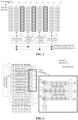
- FIG. 2 is a schematic structural diagram of a memory structure in an embodiment of the present disclosure.
- the number of spare memory arrays 14 is two, which are respectively disposed beside the two memory arrays 11 located at the edge.
- the number of the first sense amplifier arrays 15 is also two. Referring to the embodiment shown in FIG. 2 , the number of the spare memory arrays 14 is the same as the number of the first sense amplifier arrays 15.
- the first sense amplifier arrays 15 can be connected according to the above rules. It can be understood that when more than two spare memory arrays 14 are provided, other spare memory arrays 14 may be provided beside the spare memory arrays 14 shown in FIG. 2 . Same as FIG.
- the first sense amplifier array 15 can be arranged either on the right side of the spare memory array 14 or on the left side of the spare memory array 14, that is, the relative position of the first sense amplifier array 15 and the spare memory array 14. It can be interchanged, and the present disclosure does not make any special limitation to this.
- the structure shown in FIG. 1 or FIG. 2 can realize the replacement of the faulty memory array when the memory array fails.
- the memory array is faulty according to the detection result of the memory array detection circuit. For example, when a memory product is detected, the faulty memory array can be determined according to the memory array failure message generated by the detection; or, during the use of the memory product, it can be triggered in various ways (for example, timing or each power-on startup, etc.) to detect memory arrays to determine memory array failures.
- a memory array usually has multiple memory sub-arrays (blocks), and each memory sub-array usually has multiple memory cells (cells), it can be determined how many memory cells or how many memory sub-arrays according to the general settings of the product, when there is a failure (e.g. 30% failure), the memory array is determined to be faulty.
- the embodiment of the present disclosure does not limit the specific trigger logic for judging the memory failure.
- the spare memory arrays can be used to replace the failed memory arrays.
- the location of the failed memory array can be critical (e.g., middle or edge) or damaged (e.g., what percentage of memory cells or memory sub-array failure), determine which failed memory arrays to replace with spare memory arrays.
- FIG. 3 is a schematic structural diagram of a memory structure in an embodiment of the present disclosure.
- each memory array 11 includes a plurality of memory sub-arrays 111 arranged along the second direction
- the odd-numbered sense amplifier array 12 includes a plurality of odd-numbered sense amplifier sub-arrays 121
- the even-numbered sensitive amplifier sub-arrays 131 The even-numbered sense amplifier array 13 includes a plurality of even-numbered sense amplifier sub-arrays 131, and the odd-numbered sense amplifier sub-arrays 121 or the even-numbered sense amplifier sub-arrays 131 correspond to the memory sub-array 111.
- Each odd-numbered sense amplifier sub-arrays 121 is electrically connected to a plurality of odd-numbered global signal lines through an odd-numbered read-write conversion circuit, and all odd-numbered read-write conversion circuits corresponding to an odd-numbered sense amplifier array 12 constitute an odd-numbered read-write conversion circuit array 16; each even-numbered sense amplifier sub-arrays 131 are electrically connected to a plurality of even-numbered global signal line through an even-numbered read-write conversion circuit, and all even-numbered read-write conversion circuits corresponding to one even-numbered sense amplifier array 13 constitute an even-numbered read-write conversion circuit array 17.
- the spare memory array 14 includes a plurality of first spare memory sub-arrays 141, the first sense amplifier array 15 includes a plurality of first sense amplifier sub-arrays 151, and each first spare memory sub-array 141 corresponds to a first sense amplifier sub-array 151.
- Each first sense amplifier sub-array 151 is electrically connected to both the odd-numbered global signal line and the even-numbered global signal line through a spare read-write conversion circuit, and the spare read-write conversion circuit corresponding to the first sense amplifier array 15 forms a spare read-write conversion circuit array 18.
- the odd-numbered read-write conversion circuit array 16 is connected to the odd-numbered read control signal line and the odd-numbered write control signal line
- the even-numbered read-write conversion circuit array 17 is connected to the even-numbered read control signal line and the even-numbered write control signal line.
- the spare read-write conversion circuit array 18 is simultaneously connected to odd-numbered read control signal lines, odd-numbered write control signal lines, even-numbered read control signal lines, and even-numbered write control signal lines, each of which is not shown in the figure.
- FIG. 4 is a schematic diagram of a memory array control circuit.
- the memory array control circuit mainly includes a row decoding and control circuit 41 (XDEC, X Decoder), a column decoding circuit 42 (YDEC, Y Decoder), a read amplifier circuit and a write driver 43.
- the column decoding circuit 42 is used for providing a column selection signal (CSL, Column Select).
- the read amplifier circuit and the write driver 43 include a second sense amplifier (SSA) and a write driver (write driver). Both the read amplifier circuit and the write driver circuit are connected to the global signal line YIO and the complementary global signal line YIO#.
- the global signal line YIO and the complementary global signal line YIO# appear in pairs, and a pair of global signal lines YIO and the complementary global signal line YIO# constitute a group of signals corresponding to the odd-numbered global signal lines shown in FIG. 1, FIG. 2 or FIG. 3 line or a group of signal lines corresponding to the even-numbered global signal lines.
- the odd-numbered sense amplifier array 12 the even-numbered sense amplifier array 13
- the odd-numbered read-write conversion circuit array 16 and the even-numbered read-write conversion circuit array 17 please refer to the partial enlargement on the right side of FIG. 4 .
- the data of the corresponding memory array 11 is transmitted to the odd-numbered sense amplifier array 12 and the even-numbered sensitive amplifier array 12 located on both sides of the memory array.
- the amplifier array 13 is amplified by the odd-numbered sense amplifier array 12 and the even-numbered sense amplifier array 13, and then written back to the memory cells connected to the selected WL.
- the column decoding circuit 42 selects the corresponding sense amplifier , and the data is transmitted from a set of YIO&YIO# global signal lines to a set of Ldat&Ldat# local signal lines through a read-write conversion circuit (lrwap), Write to the sense amplifier and the connected memory unit corresponding to the read-write conversion circuit.
- a read-write conversion circuit (lrwap)
- the YDEC column decoding circuit 42 selects the corresponding sense amplifier , and the data is transmitted to a group of Ldat&Ldat# local signal lines, and then transmitted by the read-write conversion circuit (lrwap) connected to the sense amplifier .
- YIO&YIO# is a dual-phase paired mode, and the read or write modes are in opposite complementary polarities.
- each odd-numbered read-write conversion circuit 161 in FIG. 4 is connected to odd-numbered global signal lines (eg YIOn+1, YIOn+3), complementary odd-numbered global signal lines (YIOn+1#, YIOn+3#) And a group of Ldat&Ldat# signal lines, a plurality of odd-numbered read-write conversion circuits 161 constitute an odd-numbered read-write conversion circuit array 16; each even-numbered read-write conversion circuit 171 connects to a complementary even-numbered global signal line (YIOn#, YIOn+2#), a group of Ldat&Ldat# signal lines, and a plurality of even-numbered read-write conversion circuits 171 constitute an even-numbered read-write conversion circuit array 17.
- odd-numbered global signal lines eg YIOn+1, YIOn+3
- complementary odd-numbered global signal lines YIOn+1#, YIOn+3#
- a group of Ldat&Ldat# signal lines eg
- n is an even number greater than or equal to zero.
- the odd-numbered read-write conversion circuit 161 may not be connected to the complementary odd-numbered global signal line, that is, if the complementary odd-numbered global signal line is not provided.
- the even-numbered read-write conversion circuit 171 may also not be connected to the complementary even-numbered signal line.
- the odd numbered global signal line that is, the complementary even numbered global signal line is not provided, which is not specifically limited in the present disclosure.
- the odd-numbered sense amplifier array 12 or the even-numbered sense amplifier array 13 includes multiple sense amplifier sub-arrays, and each sense amplifier sub-array controls half of the memory arrays 11 on the left and right sides.
- the lines of the array are bit lines (BL, Bit Line). It can be known from FIG. 4 in combination with FIG. 3 that half of the memory cells in the spare memory array 14 are controlled by the first sense amplifier array 15 connected to the spare memory array 14. Replacing a complete memory array 11 can be achieved by using the two first sense amplifier arrays 15 to control the two spare memory arrays 14 respectively.
- control a first sense amplifier array 15 to perform data exchange with the odd-numbered global signal lines connected to the odd-numbered sense amplifier array corresponding to the faulty memory array, so as to use a spare memory array 14 Realize the replacement of the memory cells of half of the faulty memory arrays; control another first sense amplifier array 15 to perform data exchange with the even-numbered global signal lines connected to the even-numbered sense amplifier arrays corresponding to the faulty memory array, so as to use another spare memory array 14 enables replacement of the memory cells of the other half of the failed memory array.
- the embodiment of the present disclosure can also use the first sense amplifier array 15 and the spare memory array 14 to replace the two memory arrays 11 affected by the faulty sense amplifier array when the sense amplifier array is damaged.
- the sense amplifier s in the array exchange data with the odd-numbered global signal lines, so when replacing them, Half of the two first sense amplifier arrays 15 corresponding to the two spare memory arrays 14 connected to the spare memory array 14 are used as odd-numbered sense amplifier arrays, and carry out data with the odd-numbered global signal lines corresponding to the faulty odd-numbered sense amplifier arrays 12 exchange. Only when it is judged that data exchange with an affected memory array 11 is required through the faulty sense amplifier array, the word line WL is set to select the memory array 11 and a corresponding spare memory array 14, and control the connection of the spare memory array 14.
- the first sense amplifier array 15 and the odd-numbered global signal line connected to the faulty sense amplifier realize data exchange (the memory array 11 connected to the first sense amplifier 15 is not selected at this time); when exchanging data with another affected memory array 11, set the word line WL to select the memory array 11 and its corresponding other spare memory array 14, and control the first sense amplifier array 15 connected to the spare memory array 14 to be connected with the fault.
- the odd-numbered global signal lines connected to the sense amplifier realize data exchange.
- the connection between the spare memory array 14 and the word line WL is the same as the connection between the memory array 11 and the word line WL.
- the even-numbered sense amplifier array 13 fails and is used for replacement, the half of the connection between the two first sense amplifier arrays 15 corresponding to the two spare memory array 14, and the spare memory array 14 also needs to be used as an even-numbered sense amplifier array, and perform data exchange with the even-numbered global signal line corresponding to the faulty even-numbered sense amplifier array 13.
- the first sense amplifier array 15 must support both the functions of being an odd-numbered sense amplifier array and an even-numbered sense amplifier array. Therefore, the control mode of each sense amplifier in the first sense amplifier array 15 needs to be modified, that is, the spare read-write conversion circuit needs to be modified.
- FIG. 5 is a schematic diagram of the working principle of the spare read-write conversion circuit in the embodiment of the present disclosure.
- each read-write conversion circuit is connected to a pair of local signal lines Ldat and complementary local signal lines Ldat# and a pair of YIO and YIO# signal lines.
- the odd-numbered read-write conversion circuit 161 is connected to the odd-numbered global signal line YIOn+1 and the complementary odd-numbered global signal line YIOn+1#
- the even-numbered read-write conversion circuit 171 is connected to the even-numbered global signal line YIOn and the complementary even-numbered global signal line YIOn #.
- each read-write conversion circuit may only be connected to the YIO signal line, that is, in some embodiments, the odd-numbered read-write conversion circuit 161 may also not be connected to the complementary odd-numbered global signal line YIOn+1#.
- the even-numbered read-write conversion circuit 171 may also not be connected to the complementary even-numbered global signal line YIOn#, which is not specifically limited in the present disclosure.
- a pair of signal lines of the spare read-write conversion circuit 181 are connected to a spare sense amplifier sub-array 151.
- a plurality of spare read-write conversion circuits 181 corresponding to one first sense amplifier array 15 constitute a spare read-write conversion circuit array 18.
- the spare read-write conversion circuit 181 connects the odd-numbered global signal lines and the even-numbered global signal line at the same time, so that the spare memory array 14 can be controlled to flexibly replace the faulty memory array, or replace the memory array affected by the faulty sense amplifier array.
- FIG. 6 is a schematic circuit diagram of the spare read-write conversion circuit 181 in the spare read-write conversion circuit in the embodiment of the present disclosure.
- the spare read-write conversion circuit 181 may include: a even-numbered read control circuit 61 connected to the even-numbered global signal line YIOn, the even-numbered read control signal line Rdn and the complementary local signal line Ldat#;
- the even-numbered write control circuit 62 is connected to the even-numbered global signal line YIOn, the even-numbered write control signal line Wrn, the complementary local signal line Ldat#, and the local signal line Ldat;
- the even-numbered read control circuit 61 includes a first N-type transistor M1 and a second N-type transistor M2, the drain of the first N-type transistor M1 is connected to the odd-numbered global signal line YIOn+1, and the gate is connected to the complementary local signal line Ldat#, the drain of the second N-type transistor M2 is connected to the source of the first N-type transistor M1, the gate of the second N-type transistor M2 is connected to the even-numbered read control signal line Rdn, and the source of the second N-type transistor M2 is grounded.
- the even-numbered write control circuit 62 includes a third N-type transistor M3, a fourth N-type transistor M4, and a fifth N-type transistor M5.
- the first end of the third N-type transistor M3 is connected to the odd-numbered global signal line YIOn+1, and the second end is connected to the local signal line Ldat, the gate is connected to the even-numbered write control signal line Wrn, the drain of the fourth N-type transistor M4 is connected to the local signal line Ldat, the gate of the fourth N-type transistor M4 is connected to the odd-numbered global signal line YIOn+1, and the drain of the fifth N-type transistor M5 is connected to the source of the fourth N-type transistor M4, the gate of the fifth N-type transistor M5 is connected to the even-numbered write control signal line Wrn, and the source of the fifth N-type transistor M5 is grounded.
- the odd-numbered read control circuit 63 includes: a sixth N-type transistor M6 and a seventh N-type transistor M7, the drain of the sixth N-type transistor M6 is connected to the even-numbered global signal line YIOn, the gate of the sixth N-type transistor M6 is connected to the local signal line Ldat, and the drain of the seventh N-type transistor M7 is connected to the source of the sixth N-type transistor M6, the gate is connected to the odd-numbered read control signal line Rdn+1, and the source is grounded.
- the odd-numbered write control circuit 64 includes an eighth N-type transistor M8, a ninth N-type transistor M9, and a tenth N-type transistor M10.
- the first endof the eighth N-type transistor M8 is connected to the even-numbered global signal line YIOn, and the second end is connected to The complementary local signal line Ldat#, the gate is connected to the odd-numbered write control signal line Wm+1, the drain of the ninth N-type transistor M9 is connected to the complementary local signal line Ldat#, the gate is connected to the even-numbered global signal line YIOn, the tenth N
- the drain of the type transistor M10 is connected to the source of the ninth N-type transistor M9, the gate is connected to the odd-numbered write control signal line Wm+1, and the source is grounded.
- the even-numbered read control signal line Rdn enables the second N-type transistor M2 on, when the complementary local signal line Ldat# is at a high potential and the local signal line Ldat is at a low potential, the first N-type transistor M1 is turned on, and the local signal line Ldat is transmitted to the even-numbered voltage through the ground voltage connected by the second N-type transistor M2.
- the voltage of the even-numbered global signal line YIOn becomes a low level, and at this time, the even-numbered global signal line YIOn reads out the data on the local signal line Ldat.
- the complementary local signal line Ldat# is at a low level and the local signal line Ldat is at a high level
- the first N-type transistor M1 is turned off, and the ground voltage connected to the second N-type transistor M2 cannot be transmitted to the even-numbered global signal line YIOn
- the even-numbered global signal line YIOn maintains the high potential after pre-charging, and at this time, the even-numbered global signal line YIOn reads out the data on the local signal line Ldat.
- the even-numbered write control signal Wrn enables the third N-type transistor M3 and the fifth N-type transistor M5.
- the fourth N-type transistor M3 and the fifth N-type transistor M5 are enabled by the even-numbered write control signal Wrn.
- the N-type transistor M4 is turned on, the complementary local signal line Ldat# becomes a low potential, and the local signal line Ldat maintains the pre-charged high potential. If the even-numbered global signal line YIOn is at a low potential, the fourth N-type transistor M4 is turned off, and the complementary local signal line is turned off.
- the signal line Ldat# becomes a high potential after precharging, and the local signal line Ldat becomes a low potential.
- the reading and writing principles of odd-numbered bits are the same, and are not repeated here. It can be seen from the above that after receiving different read-write control signals, the spare read-write conversion circuit can read and write even-numbered or odd-numbered bits, so as to write signals of odd-numbered or even-numbered bits according to different read-write control signals.
- FIG. 7 is a schematic diagram of the spare read-write conversion circuit 181 in another embodiment of the present disclosure.
- the spare read-write conversion circuit 181 may further include a precharge circuit 71.
- the precharge circuit 71 is connected to the complementary local signal line Ldat#, the local signal line Ldat, the power supply voltage Vcc and the precharge signal Pre, and the precharge circuit 71 is used to pull up the complementary local signal line Ldat# and the local signal line Ldat, and to the complementary local signal line Ldat# and the local signal line Ldat are precharged.
- the precharge circuit 71 may include:
- the precharge circuit 71 is provided, and before writing, the first P-type transistor M11 and the second P-type transistor M12 are enabled by outputting the precharge control signal Pre, so as to provide a signal to the complementary local signal line Ldat# Precharge with local signal line Ldat.
- the threshold loss of signal transmission can also be avoided, so that the effect of signal transmission is better.
- FIG. 8 is a schematic diagram of the spare read-write conversion circuit 181 in still another embodiment of the present disclosure.
- the spare read-write conversion circuit 181 further includes a read-write auxiliary circuit 81, which is connected to the complementary local signal line Ldat#, the local signal line Ldat and the enable signal, the read/write auxiliary circuit 81 is used to amplify the complementary local signal line Ldat# and the local signal line Ldat.
- the read/write auxiliary circuit 81 includes:
- the read/write auxiliary circuit 81 can amplify the complementary local signal line Ldat# and the local signal line Ldat when the enable signal En is in the enable state, so that the signal transmission effect is better.
- the spare memory array 14 and the first sense amplifier array 15 are automatically used to replace the failed memory array, and when the sense amplifier array fails, the spare memory array 14 and the first sense amplifier array 15 are automatically used to replace the failed sensitive amplifier.
- the two memory arrays affected by the amplifier can not only effectively improve the reliability of memory products, but also improve the test success rate and yield rate of memory products, thereby reducing production costs.
- FIG. 9 is a schematic diagram of a memory structure in another embodiment of the present disclosure.
- a second spare memory sub-array 91 is further arranged in the memory array 11, and a spare sense amplifier sub-array is arranged between the second spare memory sub-arrays 91 of the adjacent memory arrays 11.
- the spare sense amplifier sub-arrays 92 located in different odd-numbered sense amplifier arrays 12 are all electrically connected to the same spare odd-numbered global signal line
- the spare sense amplifier sub-arrays 92 located in different even-numbered sense amplifier arrays 13 are all electrically connected to the same spare even-numbered global signal line.
- the spare memory array 14 also includes a second spare memory sub-array 91, the second spare memory sub-array 91 is provided with a corresponding spare first sense amplifier sub-array 93 located in the first sense amplifier array 15, and the spare first sense amplifier sub-array 93 is simultaneously connected to the spare odd-numbered global signal lines and the spare even-numbered global signal line through the spare read-write conversion circuit array 18.
- the number of second spare memory sub-arrays 91 in both the memory array 11 and the spare memory array 14 is one. In other embodiments, more second spare sub-arrays may be set in each memory array.
- the sub-array 91 is stored.
- the second spare memory sub-arrays 91 may be located at various positions in the memory arrays, and each second spare memory sub-array 91 has the same position in the respective memory arrays. In an exemplary embodiment of the present disclosure, the second spare memory sub-array 91 is located in the middle of the memory array 11 or the spare memory array 14.
- Those skilled in the art can set the quantity and location of the second spare memory sub-arrays 91 according to actual conditions, which is not particularly limited in the present disclosure.
- a column of memory sub-array B (also called a column block area) where the faulty memory sub-array is located can be disabled first, and each memory array can be used for a second spare memory sub-array A in a row to repair the replacement.
- the second spare memory sub-array A in this row includes the second spare memory sub-array 91 in each memory array 11 and the second spare memory sub-array 91 in the spare memory array 14; If the spare memory array 14 is not enabled, the second spare memory sub-array aof the column includes only the second spare memory sub-array 91 in each memory array 11.
- a row of second spare memory sub-arrays A in all memory arrays 11 can be read and written to replace the faulty memory sub-arrays
- the column where it is located stores sub-array B.
- the replacement function of column A to column B can perform the entire replacement of column A to column B, or a partial replacement. For example, when accessing one memory array, use the second spare memory sub-array in column A to replace the failed memory sub-array in column B; when accessing another memory array, use the second spare memory sub-array in column A to replace failed memory sub-array in column C.
- FIG. 10 is a schematic diagram of a memory circuit having a redundancy replacement function in an embodiment of the present disclosure.
- the memory circuit 1000 in the memory circuit 1000, an odd-numbered sense amplifier array 12 and an even-numbered sense amplifier array 13 are arranged between the memory arrays 11. A spare memory array 14 and a first sense amplifier array 15 are arranged beside the memory array 11 located at the edge.
- the memory circuit 1000 further includes a column decoding circuit (YDEC) 101, a sense amplifier data write driver circuit (YIO SA & write driver) 102, a plurality of data selectors (MUX, multiplexer) 103, a sense amplifier data write driver 102 includes a plurality of sense amplifier data writing circuits 1021.
- Each sense amplifier data writing circuit 1021 is connected to an odd-numbered global signal line 104 or an even-numbered signal line 105 and is connected to a data selector 103.
- the other end of the data selector 103 is connected to the data bus 110, and is controlled by the control logic and the column block repair logic.
- the data writing circuit 1021 of the sense amplifier writes to the odd-numbered global signal line 104 or even-numbered global signal line 105.
- the memory circuit 1000 is divided into a plurality of column blocks in the second direction, each block includes a memory sub-array and a sense amplifier sub-array located in the same column, for example, the column blocks 10B, 10C, 10D, all column blocks connected to four odd-numbered global signal lines 104 and four even-numbered global signal line 105, that is, 8-bit data can be transmitted.
- an odd-numbered sense amplifier sub-array is connected to four odd-numbered global signal lines through four read-write conversion circuits
- an even-numbered sense amplifier sub-array is connected to four even-numbered global signal line through four read-write conversion circuits.
- the number of odd-numbered global signal lines 104 and even-numbered global signal line 105 connected in each column block area may vary according to the memory capacity or memory processing capability of the memory array, and the present disclosure is not limited thereto.
- the odd-numbered global signal line 104 is electrically connected to the odd-numbered sense amplifier array 12 through the odd-numbered connection point 106 (specifically, the odd-numbered global signal line 104 is connected to the odd numbered sense amplifier sub-arrays 121 shown in FIG. 3 through the odd numbered read-write conversion circuit), the even-numbered global signal line 105 is electrically connected to the even-numbered sense amplifier array 13 through the even-numbered connection point 107 (specifically, the even-numbered global signal line 105 is connected to the even-numbered sense amplifier sub-array shown in FIG. 3 through the even-numbered read-write conversion circuit 17 connection).
- odd-numbered global signal lines 104 and the even-numbered global signal lines 105 are electrically connected to the first sense amplifier array 15 through the odd-numbered connection points 106 and the even-numbered connection points 107.
- connection methods refer to the circuits shown in FIGs. 6 to 8 . The present disclosure will not be repeated here.
- the spare column block area A includes a plurality of second spare memory sub-arrays and spare sense amplifier sub-arrays located in the same column.
- the spare column block area 10A included are a first spare memory sub-array in the spare memory array and a spare first sense amplifier sub-array in the first sense amplifier array.
- the spare sense amplifier sub-arrays located in the odd-numbered sense amplifier array 12 are all electrically connected to the same four spare odd-numbered global signal lines 108, and the spare sense amplifier sub-arrays located in the even-numbered sense amplifier array 13 are electrically connected to the same four.
- the spare even-numbered global signal line 109 and the spare first sense amplifier sub-array are electrically connected to the four spare odd-numbered global signal lines 108 and the four spare even-numbered global signal line 109 at the same time.
- the spare column block area 10A is connected to four spare odd-numbered global signal lines 108 and four even-numbered global signal line 109 in total, that is, 8 bits of data can be transmitted.
- the number of odd-numbered global signal lines 108 and even-numbered global signal line 109 connected in the spare column block area 10A may vary according to the memory capacity or memory processing capability of the memory array, which is the same as the column block areas 10B, 10C, and 10D. It can be known that, in some embodiments, the number of rank blocks may be 16 (excluding the spare rank block A).
- connection mode of the spare odd-numbered global signal line 108 or spare even-numbered global signal line 109 and the spare sense amplifier sub-array (the position where the dotted line box intersects the odd-numbered sense amplifier array 12 or the even-numbered sense amplifier array 13 in FIG. 10 is the same as the other odd-numbered global signal lines or even-numbered global signal line corresponding to the sense amplifier array where the spare sense amplifier sub-array is located are the same, and details are not described herein again.
- the relative positions and numbers of the spare column block areas 10A are only examples. In other embodiments of the present disclosure, the spare column block areas 10A may also be located at other positions, and the number may also be equal to or more than two.
- the spare column block region 10A can be used for the damaged column in the block area 10B, 10C or 10D is replaced by the entire column.
- the data selector 103 is set by the column block area replacement logic, so that the data corresponding to the damaged column block area 10B, 10C or 10D is transmitted to the spare column block area 10A, and then the data selector 103is changed by the control logic to perform data output control.
- the column block area or the spare column block area can be enabled through a column select signal (CSL, column select) corresponding to each column.
- row block repair logic can be used to control the enabling of the memory array 11, the odd-numbered sense amplifier 12, the even-numbered sense amplifier 13, the spare memory array 14, and the first sense amplifier array 15, or disabled so that the data is transferred correctly to the memory array or to a spare memory array.
- a memory including the memory structure of any preceding item.
- modules or units of the apparatus for action performance are mentioned in the above detailed description, this division is not mandatory. Indeed, according to embodiments of the present disclosure, the features and functions of two or more modules or units described above may be embodied in one module or unit. Conversely, the features and functions of one module or unit described above may be further divided into multiple modules or units to be embodied.
- the first sense amplifier array and the spare memory array are automatically used for replacement, thereby improving the reliability of the memory product and the success rate of the factory test, improving the yield of the product, and reducing the production cost and use cost of the memory product.
Landscapes
- Engineering & Computer Science (AREA)
- Microelectronics & Electronic Packaging (AREA)
- Dram (AREA)
- For Increasing The Reliability Of Semiconductor Memories (AREA)
Abstract
Description
- This present application claims the benefit of priority to
Chinese Patent Application No. 202111270751.1, filed on October 29, 2021 - The present disclosure relates to the technical field of integrated circuit manufacturing, and in particular, to a memory with higher reliability.
- As integrated circuit manufacturing process dimensions continue to shrink, especially when new processes are developed at an early stage, the yield improvement of memory products faces great challenges. How to effectively improve the yield of memory products and the repair success rate for the reliability of memory chips has become an important area in the field of memory manufacturing.
- It should be noted that the information disclosed in the above background section is only for enhancement of understanding of the background of the present disclosure, and therefore should not form the prior art.
- The present disclosure provides a memory structure and a memory improving yield, reliability, and repair success rate of the memory.
- According to a first aspect of the present disclosure, a memory structure is provided, comprising a plurality of memory arrays arranged in parallel along a first direction and extending along a second direction, wherein a sense amplifier array extending along the second direction is arranged between every two of the plurality of memory arrays, wherein the sense amplifier array comprises an odd-numbered sense amplifier array and an even-numbered sense amplifier array, wherein the odd-numbered sense amplifier array and the even-numbered sense amplifier array are alternating along a first direction, and wherein the odd-numbered sense amplifier array is connected to a plurality of odd-numbered global signal lines, and the even-numbered sense amplifier array is connected to a plurality of even-numbered global signal lines; and spare memory arrays, arranged on one side of the plurality of memory arrays at an edge in the first direction, wherein a first sense amplifier array is arranged between the memory arrays at the edge and the spare memory arrays, and wherein the first sense amplifier array is connected to both the plurality of odd-numbered global signal lines and the plurality of even-numbered global signal lines.
- According to a second aspect of the present disclosure, a memory device is provided including the memory structures described above.
- According to the present disclosure, by arranging a spare memory array and a first sense amplifier array located at the edge of the memory array and connecting the first sense amplifier array to both the odd-numbered global signal lines and the even-numbered global signal lines simultaneously, when damage occurs on the memory array or the sense amplifier array, the first sense amplifier array and the spare memory array can automatically be used for replacement, thereby improving the reliability of the memory product and the success rate of the factory test, improving the yield of the product, and reducing the production cost and use cost of memory products.
- It is to be understood that both the foregoing general description and the following detailed description are exemplary and explanatory only and are not limiting of the present disclosure.
- The accompanying drawings, which are incorporated in and constitute a part of this specification, illustrate embodiments consistent with the disclosure and together with the description serve to explain the principles of the disclosure. Obviously, the drawings in the following description are only some embodiments of the present disclosure, and for those of ordinary skill in the art, other drawings can also be obtained from these drawings without any creative effort.
-
FIG. 1 is a schematic diagram of a memory structure in an exemplary embodiment of the present disclosure. -
FIG. 2 is a schematic diagram of a memory structure in an embodiment of the present disclosure. -
FIG. 3 is a schematic structural diagram of a memory structure in an embodiment of the present disclosure. -
FIG. 4 is a schematic diagram of a memory array control circuit. -
FIG. 5 illustrates the working principle of the spare read-write conversion circuit in the embodiment of the present disclosure. -
FIG. 6 is a schematic circuit diagram of the spare read-writeconversion circuit 181 in the spare read-write conversion circuit in the embodiment of the present disclosure. -
FIG. 7 is a schematic diagram of the spare read-writeconversion circuit 181 in another embodiment of the present disclosure. -
FIG. 8 is a schematic diagram of the spare read-writeconversion circuit 181 in still another embodiment of the present disclosure. -
FIG. 9 is a schematic diagram of a memory structure in another embodiment of the present disclosure. -
FIG. 10 is a schematic diagram of a memory circuit having a redundancy replacement function in an embodiment of the present disclosure. - Example embodiments will now be described more fully with reference to the accompanying drawings. Example embodiments, however, can be embodied in various forms and should not be construed as limited to the examples set forth herein; rather, these embodiments are provided so that this disclosure will be thorough and complete, and will fully convey the concept of example embodiments to those skilled in the art. The described features, structures, or characteristics may be combined in any suitable manner in one or more embodiments. In the following description, numerous specific details are provided in order to give a thorough understanding of the embodiments of the present disclosure. However, those skilled in the art will appreciate that the technical solutions of the present disclosure may be practiced without one or more of the specific details, or other methods, components, devices, steps, etc. may be employed. In other instances, well-known solutions have not been shown or described in detail to avoid obscuring aspects of the present disclosure.
- In addition, the drawings are merely schematic illustrations of the present disclosure, and the same reference numerals in the drawings denote the same or similar parts, and thus their repeated descriptions will be omitted. Some of the block diagrams shown in the figures are functional entities, which do not necessarily correspond to physically or logically separate entities. These functional entities may be implemented in software, or in one or more hardware modules or integrated circuits, or in different networks and/or processor devices and/or microcontroller devices.
- The exemplary embodiments of the present disclosure will be described in detail below with reference to the accompanying drawings.
-
FIG. 1 is a schematic structural diagram of a memory structure according to an exemplary embodiment of the present disclosure. - Referring to
FIG. 1 , thememory structure 100 may include:
a plurality ofmemory arrays 11 arranged in parallel along the first direction and extending along the second direction, a sense amplifier array extending along the second direction is arranged between every twomemory arrays 11, and the sense amplifier array includes an odd-numberedsense amplifier array 12 and the even-numberedsense amplifier array 13, the odd-numberedsense amplifier array 12 and the even-numberedsense amplifier array 13 are staggered along the first direction, the odd-numberedsense amplifier array 12 is connected to the odd-numbered global signal line, and the even-numberedsense amplifier array 13 is connected to the even-numbered global signal line. It can be known that the aforementioned first direction is the direction in which the bit lines extend, and the aforementioned second direction is the direction in which the word lines extend. Thememory array 11 shown inFIG. 1 may be one rank (row), for example. - The
spare memory array 14 is arranged on one side of thememory array 11 located at the edge in the first direction. A firstsense amplifier array 15 is arranged between thespare memory array 14 and thememory array 11 located at the edge. Both odd-numbered global signal lines and even-numbered global signal line are connected. Since the odd-numbered global signal lines and the even-numbered global signal line are simultaneously connected, the firstsense amplifier array 15 can simultaneously control thespare memory array 14 and thememory array 11 located at the edge. When it is detected that anymemory array 11 is faulty, the firstsense amplifier array 15 can be controlled to read and write to thespare memory array 14, so as to realize the replacement of the faulty memory array. When any odd-numberedsense amplifier array 12 or even-numberedsense amplifier array 13 is detected to be faulty, the firstsense amplifier array 15 can be used to replace the faulty sense amplifier array. - Since the sense amplifier array reads and writes half of the memory array, in one embodiment, two
spare memory arrays 14 and two firstsense amplifier arrays 14 can be used to implement replacement of a failed memory array or a failed sense amplifier array. -
FIG. 2 is a schematic structural diagram of a memory structure in an embodiment of the present disclosure. - Referring to
FIG. 2 , in one embodiment, the number ofspare memory arrays 14 is two, which are respectively disposed beside the twomemory arrays 11 located at the edge. Correspondingly, the number of the firstsense amplifier arrays 15 is also two. Referring to the embodiment shown inFIG. 2 , the number of thespare memory arrays 14 is the same as the number of the firstsense amplifier arrays 15. When those skilled in the art set up morespare memory arrays 14, the firstsense amplifier arrays 15 can be connected according to the above rules. It can be understood that when more than twospare memory arrays 14 are provided, otherspare memory arrays 14 may be provided beside thespare memory arrays 14 shown inFIG. 2 . Same asFIG. 1 , the firstsense amplifier array 15 can be arranged either on the right side of thespare memory array 14 or on the left side of thespare memory array 14, that is, the relative position of the firstsense amplifier array 15 and thespare memory array 14. It can be interchanged, and the present disclosure does not make any special limitation to this. - In practical applications, the structure shown in
FIG. 1 or FIG. 2 can realize the replacement of the faulty memory array when the memory array fails. - It can be determined that the memory array is faulty according to the detection result of the memory array detection circuit. For example, when a memory product is detected, the faulty memory array can be determined according to the memory array failure message generated by the detection; or, during the use of the memory product, it can be triggered in various ways (for example, timing or each power-on startup, etc.) to detect memory arrays to determine memory array failures.
- Since a memory array usually has multiple memory sub-arrays (blocks), and each memory sub-array usually has multiple memory cells (cells), it can be determined how many memory cells or how many memory sub-arrays according to the general settings of the product, when there is a failure (e.g. 30% failure), the memory array is determined to be faulty. The embodiment of the present disclosure does not limit the specific trigger logic for judging the memory failure.
- There can be one or more failed memory arrays. When the number of the failed memory arrays is less than half the number of the spare memory arrays, the spare memory arrays can be used to replace the failed memory arrays. When the number of failed memory arrays is more than or equal to one-half the number of spare memory arrays, the location of the failed memory array can be critical (e.g., middle or edge) or damaged (e.g., what percentage of memory cells or memory sub-array failure), determine which failed memory arrays to replace with spare memory arrays.
- In order to further illustrate the replacement functions of the
spare memory array 14 and the firstsense amplifier array 15 in the present disclosure, the connection relationship of the data lines in the exemplary embodiment of the present disclosure is described below with reference toFIG. 3 and FIG. 4 . -
FIG. 3 is a schematic structural diagram of a memory structure in an embodiment of the present disclosure. - Referring to
FIG. 3 , in one embodiment, eachmemory array 11 includes a plurality ofmemory sub-arrays 111 arranged along the second direction, the odd-numberedsense amplifier array 12 includes a plurality of odd-numberedsense amplifier sub-arrays 121, and the even-numberedsensitive amplifier sub-arrays 131. The even-numberedsense amplifier array 13 includes a plurality of even-numberedsense amplifier sub-arrays 131, and the odd-numberedsense amplifier sub-arrays 121 or the even-numberedsense amplifier sub-arrays 131 correspond to thememory sub-array 111. - Each odd-numbered
sense amplifier sub-arrays 121 is electrically connected to a plurality of odd-numbered global signal lines through an odd-numbered read-write conversion circuit, and all odd-numbered read-write conversion circuits corresponding to an odd-numberedsense amplifier array 12 constitute an odd-numbered read-writeconversion circuit array 16; each even-numberedsense amplifier sub-arrays 131 are electrically connected to a plurality of even-numbered global signal line through an even-numbered read-write conversion circuit, and all even-numbered read-write conversion circuits corresponding to one even-numberedsense amplifier array 13 constitute an even-numbered read-writeconversion circuit array 17. - The
spare memory array 14 includes a plurality of firstspare memory sub-arrays 141, the firstsense amplifier array 15 includes a plurality of firstsense amplifier sub-arrays 151, and each firstspare memory sub-array 141 corresponds to a firstsense amplifier sub-array 151. Each firstsense amplifier sub-array 151 is electrically connected to both the odd-numbered global signal line and the even-numbered global signal line through a spare read-write conversion circuit, and the spare read-write conversion circuit corresponding to the firstsense amplifier array 15 forms a spare read-writeconversion circuit array 18. It can be understood that the odd-numbered read-writeconversion circuit array 16 is connected to the odd-numbered read control signal line and the odd-numbered write control signal line, and the even-numbered read-writeconversion circuit array 17 is connected to the even-numbered read control signal line and the even-numbered write control signal line. The spare read-writeconversion circuit array 18 is simultaneously connected to odd-numbered read control signal lines, odd-numbered write control signal lines, even-numbered read control signal lines, and even-numbered write control signal lines, each of which is not shown in the figure. -
FIG. 4 is a schematic diagram of a memory array control circuit. - In
FIG. 4 , the memory array control circuit mainly includes a row decoding and control circuit 41 (XDEC, X Decoder), a column decoding circuit 42 (YDEC, Y Decoder), a read amplifier circuit and a write driver 43. Thecolumn decoding circuit 42 is used for providing a column selection signal (CSL, Column Select). The read amplifier circuit and the write driver 43 include a second sense amplifier (SSA) and a write driver (write driver). Both the read amplifier circuit and the write driver circuit are connected to the global signal line YIO and the complementary global signal line YIO#. The global signal line YIO and the complementary global signal line YIO# appear in pairs, and a pair of global signal lines YIO and the complementary global signal line YIO# constitute a group of signals corresponding to the odd-numbered global signal lines shown inFIG. 1, FIG. 2 orFIG. 3 line or a group of signal lines corresponding to the even-numbered global signal lines. For the relationship between the global signal lines and thememory array 11, the odd-numberedsense amplifier array 12, the even-numberedsense amplifier array 13, the odd-numbered read-writeconversion circuit array 16 and the even-numbered read-writeconversion circuit array 17, please refer to the partial enlargement on the right side ofFIG. 4 . - When a WL (Word Line) is selected by the XDEC line decoder and
control circuit 41, the data of thecorresponding memory array 11 is transmitted to the odd-numberedsense amplifier array 12 and the even-numberedsensitive amplifier array 12 located on both sides of the memory array. Theamplifier array 13 is amplified by the odd-numberedsense amplifier array 12 and the even-numberedsense amplifier array 13, and then written back to the memory cells connected to the selected WL. When the data needs to be changed or rewritten, thecolumn decoding circuit 42 selects the corresponding sense amplifier , and the data is transmitted from a set of YIO&YIO# global signal lines to a set of Ldat&Ldat# local signal lines through a read-write conversion circuit (lrwap), Write to the sense amplifier and the connected memory unit corresponding to the read-write conversion circuit. When data is read out, the direction of data transmission is reversed. The YDECcolumn decoding circuit 42 selects the corresponding sense amplifier , and the data is transmitted to a group of Ldat&Ldat# local signal lines, and then transmitted by the read-write conversion circuit (lrwap) connected to the sense amplifier . to a group of YIO&YIO# global signal lines, and finally amplified and output by the SSA in the read amplifying circuit and the write driver 43. When working, YIO&YIO# is a dual-phase paired mode, and the read or write modes are in opposite complementary polarities. - It can be seen that each odd-numbered read-
write conversion circuit 161 inFIG. 4 is connected to odd-numbered global signal lines (eg YIOn+ 1, YIOn+3), complementary odd-numbered global signal lines (YIOn+1#, YIOn+3#) And a group of Ldat&Ldat# signal lines, a plurality of odd-numbered read-write conversion circuits 161 constitute an odd-numbered read-writeconversion circuit array 16; each even-numbered read-write conversion circuit 171 connects to a complementary even-numbered global signal line (YIOn#, YIOn+2#), a group of Ldat&Ldat# signal lines, and a plurality of even-numbered read-write conversion circuits 171 constitute an even-numbered read-writeconversion circuit array 17. The above n is an even number greater than or equal to zero. In some embodiments, the odd-numbered read-write conversion circuit 161 may not be connected to the complementary odd-numbered global signal line, that is, if the complementary odd-numbered global signal line is not provided. Similarly, the even-numbered read-write conversion circuit 171 may also not be connected to the complementary even-numbered signal line. The odd numbered global signal line, that is, the complementary even numbered global signal line is not provided, which is not specifically limited in the present disclosure. - From the perspective of the memory unit, the odd-numbered
sense amplifier array 12 or the even-numberedsense amplifier array 13 includes multiple sense amplifier sub-arrays, and each sense amplifier sub-array controls half of thememory arrays 11 on the left and right sides. The lines of the array are bit lines (BL, Bit Line). It can be known fromFIG. 4 in combination withFIG. 3 that half of the memory cells in thespare memory array 14 are controlled by the firstsense amplifier array 15 connected to thespare memory array 14. Replacing acomplete memory array 11 can be achieved by using the two firstsense amplifier arrays 15 to control the twospare memory arrays 14 respectively. - Specifically, when a
memory array 11 fails, control a firstsense amplifier array 15 to perform data exchange with the odd-numbered global signal lines connected to the odd-numbered sense amplifier array corresponding to the faulty memory array, so as to use aspare memory array 14 Realize the replacement of the memory cells of half of the faulty memory arrays; control another firstsense amplifier array 15 to perform data exchange with the even-numbered global signal lines connected to the even-numbered sense amplifier arrays corresponding to the faulty memory array, so as to use anotherspare memory array 14 enables replacement of the memory cells of the other half of the failed memory array. - In addition, the embodiment of the present disclosure can also use the first
sense amplifier array 15 and thespare memory array 14 to replace the twomemory arrays 11 affected by the faulty sense amplifier array when the sense amplifier array is damaged. - When a sense amplifier array (whether it is an odd-numbered
sense amplifier array 12 or an even-numbered sense amplifier array 13) is damaged, half of the memory cells in the twomemory arrays 11 it controls are affected. Therefore, when it is determined that the sense amplifier array is faulty, onespare memory array 14 can be used to replace half of the memory cells in thememory array 11 that cannot function properly due to the faulty sense amplifier , and anotherspare memory array 14 can be used to replace half of the memory cells that are affected by the faulty sense amplifier . The other half of the memory cells in thememory array 11 in normal operation. - During specific implementation, if a certain whole sense amplifier array is faulty, for example, the odd-numbered
sense amplifier array 12 fails, the sense amplifier s in the array exchange data with the odd-numbered global signal lines, so when replacing them, Half of the two firstsense amplifier arrays 15 corresponding to the twospare memory arrays 14 connected to thespare memory array 14 are used as odd-numbered sense amplifier arrays, and carry out data with the odd-numbered global signal lines corresponding to the faulty odd-numberedsense amplifier arrays 12 exchange. Only when it is judged that data exchange with anaffected memory array 11 is required through the faulty sense amplifier array, the word line WL is set to select thememory array 11 and a correspondingspare memory array 14, and control the connection of thespare memory array 14. The firstsense amplifier array 15 and the odd-numbered global signal line connected to the faulty sense amplifier realize data exchange (thememory array 11 connected to thefirst sense amplifier 15 is not selected at this time); when exchanging data with another affectedmemory array 11, set the word line WL to select thememory array 11 and its corresponding otherspare memory array 14, and control the firstsense amplifier array 15 connected to thespare memory array 14 to be connected with the fault. The odd-numbered global signal lines connected to the sense amplifier s realize data exchange. The connection between thespare memory array 14 and the word line WL is the same as the connection between thememory array 11 and the word line WL. - In the same way, if the even-numbered
sense amplifier array 13 fails and is used for replacement, the half of the connection between the two firstsense amplifier arrays 15 corresponding to the twospare memory array 14, and thespare memory array 14 also needs to be used as an even-numbered sense amplifier array, and perform data exchange with the even-numbered global signal line corresponding to the faulty even-numberedsense amplifier array 13. - As can be seen from the above description, the first
sense amplifier array 15 must support both the functions of being an odd-numbered sense amplifier array and an even-numbered sense amplifier array. Therefore, the control mode of each sense amplifier in the firstsense amplifier array 15 needs to be modified, that is, the spare read-write conversion circuit needs to be modified. -
FIG. 5 is a schematic diagram of the working principle of the spare read-write conversion circuit in the embodiment of the present disclosure. - Referring to
FIG. 5 , a pair of local signal lines Ldat and complementary local signal lines Ldat# connected to the odd-numbered read-write conversion circuit 161 or the even-numbered read-write conversion circuit 171 are connected to an odd-numberedsense amplifier sub-arrays 121 or an even-numberedsensitive amplifier sub-array 131. In the even-numberedsense amplifier sub-arrays 131, each read-write conversion circuit is connected to a pair of local signal lines Ldat and complementary local signal lines Ldat# and a pair of YIO and YIO# signal lines. The odd-numbered read-write conversion circuit 161 is connected to the odd-numbered global signal line YIOn+1 and the complementary odd-numbered global signal line YIOn+1#, and the even-numbered read-write conversion circuit 171 is connected to the even-numbered global signal line YIOn and the complementary even-numbered global signal line YIOn #. In some embodiments, each read-write conversion circuit may only be connected to the YIO signal line, that is, in some embodiments, the odd-numbered read-write conversion circuit 161 may also not be connected to the complementary odd-numbered global signal line YIOn+1#. In principle, the even-numbered read-write conversion circuit 171 may also not be connected to the complementary even-numbered global signal line YIOn#, which is not specifically limited in the present disclosure. - A pair of signal lines of the spare read-
write conversion circuit 181 are connected to a sparesense amplifier sub-array 151. A plurality of spare read-write conversion circuits 181 corresponding to one firstsense amplifier array 15 constitute a spare read-writeconversion circuit array 18. The spare read-write conversion circuit 181 connects the odd-numbered global signal lines and the even-numbered global signal line at the same time, so that thespare memory array 14 can be controlled to flexibly replace the faulty memory array, or replace the memory array affected by the faulty sense amplifier array. -
FIG. 6 is a schematic circuit diagram of the spare read-write conversion circuit 181 in the spare read-write conversion circuit in the embodiment of the present disclosure. - Referring to
FIG. 6 , the spare read-write conversion circuit 181 may include:
a even-numberedread control circuit 61 connected to the even-numbered global signal line YIOn, the even-numbered read control signal line Rdn and the complementary local signal line Ldat#; - The even-numbered
write control circuit 62 is connected to the even-numbered global signal line YIOn, the even-numbered write control signal line Wrn, the complementary local signal line Ldat#, and the local signal line Ldat; - an odd-numbered
read control circuit 63 connected to the odd-numbered global signalline YIOn+ 1, the odd-numbered read control signal line Rdn+1 and the local signal line Ldat; and - an odd-numbered
write control circuit 64 connected to the odd-numbered global signalline YIOn+ 1, the odd-numbered write control signalline Wrn+ 1, the complementary local signal line Ldat#, and the local signal line Ldat. - In the embodiment shown in
FIG. 6 , the even-numberedread control circuit 61 includes a first N-type transistor M1 and a second N-type transistor M2, the drain of the first N-type transistor M1 is connected to the odd-numbered global signalline YIOn+ 1, and the gate is connected to the complementary local signal line Ldat#, the drain of the second N-type transistor M2 is connected to the source of the first N-type transistor M1, the gate of the second N-type transistor M2 is connected to the even-numbered read control signal line Rdn, and the source of the second N-type transistor M2 is grounded. - The even-numbered
write control circuit 62 includes a third N-type transistor M3, a fourth N-type transistor M4, and a fifth N-type transistor M5. The first end of the third N-type transistor M3 is connected to the odd-numbered global signalline YIOn+ 1, and the second end is connected to the local signal line Ldat, the gate is connected to the even-numbered write control signal line Wrn, the drain of the fourth N-type transistor M4 is connected to the local signal line Ldat, the gate of the fourth N-type transistor M4 is connected to the odd-numbered global signalline YIOn+ 1, and the drain of the fifth N-type transistor M5 is connected to the source of the fourth N-type transistor M4, the gate of the fifth N-type transistor M5 is connected to the even-numbered write control signal line Wrn, and the source of the fifth N-type transistor M5 is grounded. - The odd-numbered
read control circuit 63 includes: a sixth N-type transistor M6 and a seventh N-type transistor M7, the drain of the sixth N-type transistor M6 is connected to the even-numbered global signal line YIOn, the gate of the sixth N-type transistor M6 is connected to the local signal line Ldat, and the drain of the seventh N-type transistor M7 is connected to the source of the sixth N-type transistor M6, the gate is connected to the odd-numbered read control signalline Rdn+ 1, and the source is grounded. - The odd-numbered
write control circuit 64 includes an eighth N-type transistor M8, a ninth N-type transistor M9, and a tenth N-type transistor M10. The first endof the eighth N-type transistor M8 is connected to the even-numbered global signal line YIOn, and the second end is connected to The complementary local signal line Ldat#, the gate is connected to the odd-numbered write control signal line Wm+1, the drain of the ninth N-type transistor M9 is connected to the complementary local signal line Ldat#, the gate is connected to the even-numbered global signal line YIOn, the tenth N The drain of the type transistor M10 is connected to the source of the ninth N-type transistor M9, the gate is connected to the odd-numbered write control signal line Wm+1, and the source is grounded. - When the circuit is in an even-numbered read state, after pre-charging the even-numbered global signal line YIOn (the pre-charging circuit of the signal line YIO is not shown), the even-numbered read control signal line Rdn enables the second N-type transistor M2 on, when the complementary local signal line Ldat# is at a high potential and the local signal line Ldat is at a low potential, the first N-type transistor M1 is turned on, and the local signal line Ldat is transmitted to the even-numbered voltage through the ground voltage connected by the second N-type transistor M2. In the bit global signal line YIOn, the voltage of the even-numbered global signal line YIOn becomes a low level, and at this time, the even-numbered global signal line YIOn reads out the data on the local signal line Ldat. When the complementary local signal line Ldat# is at a low level and the local signal line Ldat is at a high level, the first N-type transistor M1 is turned off, and the ground voltage connected to the second N-type transistor M2 cannot be transmitted to the even-numbered global signal line YIOn, the even-numbered global signal line YIOn maintains the high potential after pre-charging, and at this time, the even-numbered global signal line YIOn reads out the data on the local signal line Ldat. When the circuit is in the write state of the even bits, the even-numbered write control signal Wrn enables the third N-type transistor M3 and the fifth N-type transistor M5. At this time, if the even-numbered global signal line YIOn is at a high level, the fourth N-type transistor M3 and the fifth N-type transistor M5 are enabled by the even-numbered write control signal Wrn. The N-type transistor M4 is turned on, the complementary local signal line Ldat# becomes a low potential, and the local signal line Ldat maintains the pre-charged high potential. If the even-numbered global signal line YIOn is at a low potential, the fourth N-type transistor M4 is turned off, and the complementary local signal line is turned off. The signal line Ldat# becomes a high potential after precharging, and the local signal line Ldat becomes a low potential. The reading and writing principles of odd-numbered bits are the same, and are not repeated here. It can be seen from the above that after receiving different read-write control signals, the spare read-write conversion circuit can read and write even-numbered or odd-numbered bits, so as to write signals of odd-numbered or even-numbered bits according to different read-write control signals. The spare memory array or read from the spare memory array.
-
FIG. 7 is a schematic diagram of the spare read-write conversion circuit 181 in another embodiment of the present disclosure. - Referring to
FIG. 7 , in an exemplary embodiment of the present disclosure, the spare read-write conversion circuit 181 may further include aprecharge circuit 71. Theprecharge circuit 71 is connected to the complementary local signal line Ldat#, the local signal line Ldat, the power supply voltage Vcc and the precharge signal Pre, and theprecharge circuit 71 is used to pull up the complementary local signal line Ldat# and the local signal line Ldat, and to the complementary local signal line Ldat# and the local signal line Ldat are precharged. - In the embodiment shown in
FIG. 7 , theprecharge circuit 71 may include: - a first P-type transistor M11, the source of M11 is connected to the power supply voltage Vcc, the gate is connected to the precharge control signal Pre, and the drain is connected to the local signal line Ldat;
- a second P-type transistor M12, the source of M11 is connected to the power supply voltage Vcc, the gate is connected to the precharge control signal Pre, and the drain is connected to the complementary local signal line Ldat#; and
- a third P-type transistor M13 which has a first end connected to the complementary local signal line Ldat#, a second end connected to the local signal line Ldat, and a control end connected to the precharge control signal Pre.
- In the embodiment of the present disclosure, the
precharge circuit 71 is provided, and before writing, the first P-type transistor M11 and the second P-type transistor M12 are enabled by outputting the precharge control signal Pre, so as to provide a signal to the complementary local signal line Ldat# Precharge with local signal line Ldat. - By pulling up the complementary local signal line Ldat# and the local signal line Ldat, the threshold loss of signal transmission can also be avoided, so that the effect of signal transmission is better.
-
FIG. 8 is a schematic diagram of the spare read-write conversion circuit 181 in still another embodiment of the present disclosure. - Referring to
FIG. 8 , in an exemplary embodiment of the present disclosure, the spare read-write conversion circuit 181 further includes a read-write auxiliary circuit 81, which is connected to the complementary local signal line Ldat#, the local signal line Ldat and the enable signal, the read/writeauxiliary circuit 81 is used to amplify the complementary local signal line Ldat# and the local signal line Ldat. - In the embodiment shown in
FIG. 8 , the read/writeauxiliary circuit 81 includes: - a fourth P-type transistor M14, the source is connected to the power supply voltage;
- a fifth P-type transistor M15, the source is connected to the power supply voltage, the gate is connected to the source M14 of the fourth P-type transistor, and the source is connected to the gate of the fourth P-type transistor M14;
- an eleventh N-type transistor M16, the drain is connected to the source of the fourth P-type transistor M14, and the gate is connected to the source of the fifth P-type transistor M15;
- a twelfth N-type transistor M17, the drain is connected to the source of the fifth P-type transistor M15, the gate is connected to the source of the fourth P-type transistor M14, and the source is connected to the source of the eleventh N-type transistor M16; and
- a thirteenth N-type transistor M18, the drain is connected to the source of the eleventh N-type transistor M16, the gate is connected to the enable signal En, and the source is grounded.
- The read/write
auxiliary circuit 81 can amplify the complementary local signal line Ldat# and the local signal line Ldat when the enable signal En is in the enable state, so that the signal transmission effect is better. - When the memory array fails, the
spare memory array 14 and the firstsense amplifier array 15 are automatically used to replace the failed memory array, and when the sense amplifier array fails, thespare memory array 14 and the firstsense amplifier array 15 are automatically used to replace the failed sensitive amplifier. The two memory arrays affected by the amplifier can not only effectively improve the reliability of memory products, but also improve the test success rate and yield rate of memory products, thereby reducing production costs. -
FIG. 9 is a schematic diagram of a memory structure in another embodiment of the present disclosure. - Referring to
FIG. 9 , in an embodiment of the present disclosure, a secondspare memory sub-array 91 is further arranged in thememory array 11, and a spare sense amplifier sub-array is arranged between the second spare memory sub-arrays 91 of theadjacent memory arrays 11. The sparesense amplifier sub-arrays 92 located in different odd-numberedsense amplifier arrays 12 are all electrically connected to the same spare odd-numbered global signal line, and the sparesense amplifier sub-arrays 92 located in different even-numberedsense amplifier arrays 13 are all electrically connected to the same spare even-numbered global signal line. - Meanwhile, the
spare memory array 14 also includes a secondspare memory sub-array 91, the secondspare memory sub-array 91 is provided with a corresponding spare firstsense amplifier sub-array 93 located in the firstsense amplifier array 15, and the spare firstsense amplifier sub-array 93 is simultaneously connected to the spare odd-numbered global signal lines and the spare even-numbered global signal line through the spare read-writeconversion circuit array 18. - In the embodiment shown in
FIG. 9 , the number of second spare memory sub-arrays 91 in both thememory array 11 and thespare memory array 14 is one. In other embodiments, more second spare sub-arrays may be set in each memory array. The sub-array 91 is stored. In addition, the second spare memory sub-arrays 91 may be located at various positions in the memory arrays, and each secondspare memory sub-array 91 has the same position in the respective memory arrays. In an exemplary embodiment of the present disclosure, the secondspare memory sub-array 91 is located in the middle of thememory array 11 or thespare memory array 14. Those skilled in the art can set the quantity and location of the second spare memory sub-arrays 91 according to actual conditions, which is not particularly limited in the present disclosure. - Referring to
FIG. 9 , when a large failure occurs in a key position related to a column, a column of memory sub-array B (also called a column block area) where the faulty memory sub-array is located can be disabled first, and each memory array can be used for a second spare memory sub-array A in a row to repair the replacement. At this time, if thespare memory array 14 is enabled, the second spare memory sub-array A in this row includes the secondspare memory sub-array 91 in eachmemory array 11 and the secondspare memory sub-array 91 in thespare memory array 14; If thespare memory array 14 is not enabled, the second spare memory sub-array aof the column includes only the secondspare memory sub-array 91 in eachmemory array 11. - In the peripheral circuit, when data needs to be written to a row of memory sub-arrays B including the faulty memory sub-arrays, a row of second spare memory sub-arrays A in all
memory arrays 11 can be read and written to replace the faulty memory sub-arrays The column where it is located stores sub-array B. When reading, it is necessary to control to output the YIO data read out from a column of the second spare memory sub-array A to a position corresponding to the replaced column of memory sub-arrays. - The replacement function of column A to column B can perform the entire replacement of column A to column B, or a partial replacement. For example, when accessing one memory array, use the second spare memory sub-array in column A to replace the failed memory sub-array in column B; when accessing another memory array, use the second spare memory sub-array in column A to replace failed memory sub-array in column C.
-
FIG. 10 is a schematic diagram of a memory circuit having a redundancy replacement function in an embodiment of the present disclosure. - Referring to
FIG. 10 , in thememory circuit 1000, an odd-numberedsense amplifier array 12 and an even-numberedsense amplifier array 13 are arranged between thememory arrays 11. Aspare memory array 14 and a firstsense amplifier array 15 are arranged beside thememory array 11 located at the edge. In addition, thememory circuit 1000 further includes a column decoding circuit (YDEC) 101, a sense amplifier data write driver circuit (YIO SA & write driver) 102, a plurality of data selectors (MUX, multiplexer) 103, a sense amplifier data writedriver 102 includes a plurality of sense amplifierdata writing circuits 1021. - Each sense amplifier
data writing circuit 1021 is connected to an odd-numberedglobal signal line 104 or an even-numberedsignal line 105 and is connected to adata selector 103. The other end of thedata selector 103 is connected to thedata bus 110, and is controlled by the control logic and the column block repair logic. Thedata writing circuit 1021 of the sense amplifier writes to the odd-numberedglobal signal line 104 or even-numberedglobal signal line 105. - The
memory circuit 1000 is divided into a plurality of column blocks in the second direction, each block includes a memory sub-array and a sense amplifier sub-array located in the same column, for example, the column blocks 10B, 10C, 10D, all column blocks connected to four odd-numberedglobal signal lines 104 and four even-numberedglobal signal line 105, that is, 8-bit data can be transmitted. Specifically, an odd-numbered sense amplifier sub-array is connected to four odd-numbered global signal lines through four read-write conversion circuits, and an even-numbered sense amplifier sub-array is connected to four even-numbered global signal line through four read-write conversion circuits. The number of odd-numberedglobal signal lines 104 and even-numberedglobal signal line 105 connected in each column block area may vary according to the memory capacity or memory processing capability of the memory array, and the present disclosure is not limited thereto. - The odd-numbered
global signal line 104 is electrically connected to the odd-numberedsense amplifier array 12 through the odd-numbered connection point 106 (specifically, the odd-numberedglobal signal line 104 is connected to the odd numberedsense amplifier sub-arrays 121 shown inFIG. 3 through the odd numbered read-write conversion circuit), the even-numberedglobal signal line 105 is electrically connected to the even-numberedsense amplifier array 13 through the even-numbered connection point 107 (specifically, the even-numberedglobal signal line 105 is connected to the even-numbered sense amplifier sub-array shown inFIG. 3 through the even-numbered read-write conversion circuit 17 connection). In addition, the odd-numberedglobal signal lines 104 and the even-numberedglobal signal lines 105 are electrically connected to the firstsense amplifier array 15 through the odd-numbered connection points 106 and the even-numbered connection points 107. For connection methods, refer to the circuits shown inFIGs. 6 to 8 . The present disclosure will not be repeated here. - The spare column block area A includes a plurality of second spare memory sub-arrays and spare sense amplifier sub-arrays located in the same column. In some embodiments, when the spare memory array and the first sense amplifier array are enabled, the spare column block area 10A included are a first spare memory sub-array in the spare memory array and a spare first sense amplifier sub-array in the first sense amplifier array. The spare sense amplifier sub-arrays located in the odd-numbered
sense amplifier array 12 are all electrically connected to the same four spare odd-numberedglobal signal lines 108, and the spare sense amplifier sub-arrays located in the even-numberedsense amplifier array 13 are electrically connected to the same four. The spare even-numberedglobal signal line 109 and the spare first sense amplifier sub-array are electrically connected to the four spare odd-numberedglobal signal lines 108 and the four spare even-numberedglobal signal line 109 at the same time. The spare column block area 10A is connected to four spare odd-numberedglobal signal lines 108 and four even-numberedglobal signal line 109 in total, that is, 8 bits of data can be transmitted. The number of odd-numberedglobal signal lines 108 and even-numberedglobal signal line 109 connected in the spare column block area 10A may vary according to the memory capacity or memory processing capability of the memory array, which is the same as the column block areas 10B, 10C, and 10D. It can be known that, in some embodiments, the number of rank blocks may be 16 (excluding the spare rank block A). The connection mode of the spare odd-numberedglobal signal line 108 or spare even-numberedglobal signal line 109 and the spare sense amplifier sub-array (the position where the dotted line box intersects the odd-numberedsense amplifier array 12 or the even-numberedsense amplifier array 13 inFIG. 10 is the same as the other odd-numbered global signal lines or even-numbered global signal line corresponding to the sense amplifier array where the spare sense amplifier sub-array is located are the same, and details are not described herein again. - The relative positions and numbers of the spare column block areas 10A are only examples. In other embodiments of the present disclosure, the spare column block areas 10A may also be located at other positions, and the number may also be equal to or more than two.
- When any one of the column block regions 10B, 10C, 10D is damaged (e.g., the number of inoperable memory sub-arrays and/or sense amplifier sub-arrays exceeds a preset threshold), the spare column block region 10A can be used for the damaged column in the block area 10B, 10C or 10D is replaced by the entire column. During specific execution, the
data selector 103 is set by the column block area replacement logic, so that the data corresponding to the damaged column block area 10B, 10C or 10D is transmitted to the spare column block area 10A, and then the data selector 103is changed by the control logic to perform data output control. The column block area or the spare column block area can be enabled through a column select signal (CSL, column select) corresponding to each column. - Similarly, when any one of the
memory array 11, the odd-numberedsense amplifier 12, and the even-numberedsense amplifier 13 is damaged, thespare memory array 14 and the firstsense amplifier array 15 can be used for replacement, thereby realizing the replacement in the row direction. In one embodiment, row block repair logic can be used to control the enabling of thememory array 11, the odd-numberedsense amplifier 12, the even-numberedsense amplifier 13, thespare memory array 14, and the firstsense amplifier array 15, or disabled so that the data is transferred correctly to the memory array or to a spare memory array. - Through the memory structure provided by the embodiments of the present disclosure, whether it is a large-area manufacturing error related to a column or a row, it can be repaired by replacing the entire block together, thereby improving the repair capability and chip reliability. Yield rate, success rate, especially for the early research and development of new processes is more effective.
- According to a second aspect of the present disclosure, there is provided a memory including the memory structure of any preceding item.
- It should be noted that although several modules or units of the apparatus for action performance are mentioned in the above detailed description, this division is not mandatory. Indeed, according to embodiments of the present disclosure, the features and functions of two or more modules or units described above may be embodied in one module or unit. Conversely, the features and functions of one module or unit described above may be further divided into multiple modules or units to be embodied.
- Other embodiments of the present disclosure will readily occur to those skilled in the art upon consideration of the specification and practice of the invention disclosed herein. This application is intended to cover any variations, uses, or adaptations of the present disclosure that follow the general principles of the present disclosure and include common knowledge or techniques in the technical field not disclosed by the present disclosure. The specification and examples are to be regarded as exemplary only, with the true scope and spirit of the disclosure being indicated by the claims.
- In the embodiment of the present disclosure, by arranging a spare memory array and a first sense amplifier array beside the memory array, and simultaneously connecting the first sense amplifier array to the odd-numbered global signal lines and the even-numbered global signal line, when damage of the memory array or the sense amplifier array occurs, the first sense amplifier array and the spare memory array are automatically used for replacement, thereby improving the reliability of the memory product and the success rate of the factory test, improving the yield of the product, and reducing the production cost and use cost of the memory product.
Claims (14)
- A memory structure, comprising:a plurality of memory arrays arranged in parallel along a first direction and extending along a second direction,wherein a sense amplifier array extending along the second direction is arranged between every two of the plurality of memory arrays, wherein the sense amplifier array comprises an odd-numbered sense amplifier array and an even-numbered sense amplifier array, wherein the odd-numbered sense amplifier array and the even-numbered sense amplifier array are alternating along a first direction, and wherein the odd-numbered sense amplifier array is connected to a plurality of odd-numbered global signal lines, and the even-numbered sense amplifier array is connected to a plurality of even-numbered global signal lines;
andspare memory arrays, arranged on one side of the plurality of memory arrays at an edge in the first direction, wherein a first sense amplifier array is arranged between the memory arrays at the edge and the spare memory arrays, and wherein the first sense amplifier array is connected to both the plurality of odd-numbered global signal lines and the plurality of even-numbered global signal lines. - The memory structure of claim 1, wherein each of the plurality of memory arrays comprises a plurality of memory sub-arrays arranged along the second direction, and wherein the sense amplifier array comprises a plurality of sense amplifier sub-arrays, wherein each of the plurality of the sense amplifier sub-arrays is connected to one of read-write conversion circuits, wherein the plurality of the sense amplifier sub-arrays is in one-to-one correspondence with the plurality of memory sub-arrays, wherein the odd-numbered sense amplifier array is electrically connects to the plurality of odd-numbered global signal lines through the read-write conversion circuits, and wherein the even-numbered sense amplifier array is electrically connected to the plurality of even-numbered global signal lines through the read-write conversion circuits; and
wherein each of the spare memory arrays comprises a plurality of first spare memory sub-arrays, wherein the first sense amplifier array comprises a plurality of first sense amplifier sub-arrays, and wherein each of the plurality of first spare memory sub-arrays corresponds to one of the plurality of first sense amplifier sub-arrays, wherein the first sense amplifier sub-array is electrically connected to both the plurality of odd-numbered global signal lines and the plurality of even-numbered global signal lines through a spare read-write conversion circuit. - The memory structure of claim 1, wherein a number of the spare memory arrays is two, which are respectively disposed beside two of the plurality of memory arrays located at the edge.
- The memory structure of any one of claims 1-3, wherein each of the plurality of memory arrays and the spare memory arrays comprises a second spare memory sub-array, wherein the second spare memory sub-array is arranged to be along the first direction; and
wherein the sense amplifier array further comprises a spare sense amplifier sub-array, and the spare sense amplifier sub-array is located between two adjacent second spare memory sub-arrays. - The memory structure of claim 4, wherein a number of the second spare memory sub-arrays in each of the plurality of memory arrays or the spare memory arrays is one.
- The memory structure of claim 4, wherein the spare sense amplifier sub-arrays located in the odd-numbered sense amplifier array is electrically connected to a same spare odd-numbered global signal line; and wherein the spare sense amplifier sub-arrays located in the even-numbered sense amplifier array is electrically connected to a same spare even-numbered global signal line.
- The memory structure of claim 2, wherein the spare read-write conversion circuit comprises:an even-numbered read control circuit, connected to the plurality of even-numbered global signal lines, an even-numbered read control signal line and a complementary local signal line;an even-numbered write control circuit, connected to the plurality of even-numbered global signal lines, an even-numbered write control signal line, a complementary local signal line and a local signal line;an odd-numbered read control circuit, connected to the plurality of odd-numbered global signal lines,an odd-numbered read control signal line, and the local signal line; andan odd-numbered write control circuit, connected to the plurality of odd-numbered global signal lines, an odd-numbered write control signal line, the complementary local signal line, and the local signal line.
- The memory structure of claim 7, wherein the spare read-write conversion circuit further comprises:
a precharge circuit, wherein the precharge circuit is connected to the complementary local signal line, the local signal line, a power supply voltage, and a precharge signal, and wherein the precharge circuit pulls up the complementary local signal line and the local signal line. - The memory structure of claim 7, wherein the spare read-write conversion circuit further comprises:
a read-write auxiliary circuit, wherein the read-write auxiliary circuit is connected to the complementary local signal line, the local signal line, and an enable signal, and wherein the read-write auxiliary circuit amplifies the complementary local signal line and the local signal line. - The memory structure of claim 7, wherein the even-numbered read control circuit comprises a first N-type transistor and a second N-type transistor, wherein a drain of the first N-type transistor is connected to the plurality of odd-numbered global signal lines, a gate of the first N-type transistor is connected to the complementary local signal line, a drain of the second N-type transistor is connected to a source of the first N-type transistor, a gate of the second N-type transistor is connected to the even-numbered read control signal line, and a source of the second N-type transistor is grounded;wherein the even-numbered write control circuit comprises a third N-type transistor, a fourth N-type transistor, and a fifth N-type transistor,wherein a first end of the third N-type transistor is connected to the plurality of odd-numbered global signal lines, and a second end of the third N-type transistor is connected to the local signal line, a gate of the third N-type transistor is connected to the even-numbered write control signal line,wherein a drain of the fourth N-type transistor is connected to the local signal line, a gate of the fourth N-type transistor is connected to the plurality of odd-numbered global signal lines, andwherein a drain of the fifth N-type transistors is connected to a source of the fourth N-type transistor, a gate of the fifth N-type transistors is connected to the even-numbered write control signal line, and a source of the fifth N-type transistors is grounded.
- The memory structure of claim 7, wherein the odd-numbered read control circuit comprises:the odd-numbered read control circuit comprises a sixth N-type transistor and a seventh N-type transistor, wherein a drain of the sixth N-type transistor is connected to the plurality of even-numbered global signal lines, a gate of the sixth N-type transistor is connected to the local signal line, andwherein a drain of the seventh N-type transistor is connected to a source of the sixth N-type transistor, a gate of the seventh N-type transistor is connected to the odd-numbered read control signal line, and a source of the seventh N-type transistor is grounded;wherein the odd-numbered write control circuit further comprises an eighth N-type transistor, a ninth N-type transistor and a tenth N-type transistor, wherein a first end of the eighth N-type transistor is connected to the plurality of even-numbered global signal lines, a second end of the eighth N-type transistor is connected to the complementary local signal line, and a gate of the eighth N-type transistor is connected to the odd-numbered write control signal line, wherein a drain of the ninth N-type transistor is connected to the complementary local signal line, a gate of the ninth N-type transistor is connected to the plurality of even-numbered global signal lines, andwherein a drain of the tenth N-type transistor is connected to a source of the ninth N-type transistor,a gate of the tenth N-type transistor is connected to the odd-numbered write control signal line, and a source of the tenth N-type transistor is grounded.
- The memory structure of claim 8, wherein the precharge circuit comprises:a first P-type transistor, wherein a source of the first P-type transistor is connected to a power supply voltage, a gate of the first P-type transistor is connected to a precharge control signal, and a drain of the first P-type transistor is connected to the local signal line;a second P-type transistor, wherein a source of the second P-type transistor is connected to the power supply voltage, a gate of the second P-type transistor is connected to the precharge control signal, and a drain of the second P-type transistor is connected to the complementary local signal line; anda third P-type transistor, wherein a first end of the third P-type transistor connected to the complementary local signal line, a second end of the third P-type transistor is connected to the local signal line, and a control end of the third P-type transistor is connected to the precharge control signal.
- The memory structure of claim 9, wherein the read-write auxiliary circuit comprises:a fourth P-type transistor, wherein a source of the fourth P-type transistor is connected to a power supply voltage;a fifth P-type transistor, wherein a source of the fifth P-type transistor is connected to the power supply voltage, a gate of the fifth P-type transistor is connected to a source of the fourth P-type transistor, and a source of the fifth P-type transistor is connected to a gate of the fourth P-type transistor;an eleventh N-type transistor, wherein a drain of the eleventh N-type transistor is connected to the source of the fourth P-type transistor, and a gate of the eleventh N-type transistor is connected to the source of the fifth P-type transistor;a twelfth N-type transistor, wherein a drain of the twelfth N-type transistor is connected to a source of the fifth P-type transistor, a gate of the twelfth N-type transistor is connected to a source of the fourth P-type transistor, and a source of the twelfth N-type transistor is connected to a source of the eleventh N-type transistor; anda thirteenth N-type transistor, wherein a drain of the thirteenth N-type transistor is connected to a source of the eleventh N-type transistor, a gate of the thirteenth N-type transistor is connected to the enable signal, and a source of the thirteenth N-type transistor is grounded.
- A memory, comprising the memory structure of any one of claims 1-13.
Applications Claiming Priority (2)
| Application Number | Priority Date | Filing Date | Title |
|---|---|---|---|
| CN202111270751.1A CN116072168B (en) | 2021-10-29 | 2021-10-29 | Memory structure and memory |
| PCT/CN2022/092551 WO2023071144A1 (en) | 2021-10-29 | 2022-05-12 | Memory structure and memory |
Publications (3)
| Publication Number | Publication Date |
|---|---|
| EP4418269A1 true EP4418269A1 (en) | 2024-08-21 |
| EP4418269A4 EP4418269A4 (en) | 2025-01-22 |
| EP4418269B1 EP4418269B1 (en) | 2026-05-20 |
Family
ID=86160460
Family Applications (1)
| Application Number | Title | Priority Date | Filing Date |
|---|---|---|---|
| EP22885057.4A Active EP4418269B1 (en) | 2021-10-29 | 2022-05-12 | MEMORY STRUCTURE AND MEMORY |
Country Status (4)
| Country | Link |
|---|---|
| US (1) | US12254939B2 (en) |
| EP (1) | EP4418269B1 (en) |
| CN (1) | CN116072168B (en) |
| WO (1) | WO2023071144A1 (en) |
Family Cites Families (38)
| Publication number | Priority date | Publication date | Assignee | Title |
|---|---|---|---|---|
| KR940008208B1 (en) * | 1990-12-22 | 1994-09-08 | 삼성전자주식회사 | Redundant apparatus and method of semiconductor memory device |
| KR0172393B1 (en) * | 1995-11-22 | 1999-03-30 | 김광호 | Semiconductor memory device with elastic column relief |
| US6084816A (en) * | 1998-04-16 | 2000-07-04 | Kabushiki Kaisha Toshiba | Semiconductor memory device |
| JP2000182390A (en) * | 1998-12-11 | 2000-06-30 | Mitsubishi Electric Corp | Semiconductor storage device |
| KR100339416B1 (en) * | 1999-09-15 | 2002-05-31 | 박종섭 | Nonvolatile ferroelectric memory device with column redundancy circuit and method for a relief failed address the same |
| KR100839887B1 (en) * | 2001-01-31 | 2008-06-20 | 엘피다 메모리, 아이엔씨. | Semiconductor integrated circuit device |
| JP4111762B2 (en) * | 2002-07-03 | 2008-07-02 | 株式会社ルネサステクノロジ | Semiconductor memory device |
| JP2004071093A (en) * | 2002-08-08 | 2004-03-04 | Fujitsu Ltd | Memory circuit with redundant memory cell array for easy shipping test and reduced power consumption |
| JP2004079138A (en) | 2002-08-22 | 2004-03-11 | Renesas Technology Corp | Nonvolatile semiconductor memory device |
| JP4357246B2 (en) * | 2003-09-16 | 2009-11-04 | 株式会社ルネサステクノロジ | Semiconductor memory device |
| JP4712365B2 (en) * | 2004-08-13 | 2011-06-29 | ルネサスエレクトロニクス株式会社 | Nonvolatile semiconductor memory device and semiconductor memory device |
| KR100627515B1 (en) * | 2004-10-04 | 2006-09-21 | 주식회사 하이닉스반도체 | Memory device and its test method |
| ITMI20041957A1 (en) * | 2004-10-15 | 2005-01-15 | St Microelectronics Srl | MEMORY DEVICE |
| US7142471B2 (en) * | 2005-03-31 | 2006-11-28 | Sandisk 3D Llc | Method and apparatus for incorporating block redundancy in a memory array |
| KR100699848B1 (en) * | 2005-06-21 | 2007-03-27 | 삼성전자주식회사 | A phase change memory device having an improved core structure |
| JP4547313B2 (en) * | 2005-08-01 | 2010-09-22 | 株式会社日立製作所 | Semiconductor memory device |
| JP5063912B2 (en) * | 2006-03-31 | 2012-10-31 | パナソニック株式会社 | Semiconductor memory device |
| JP5114894B2 (en) * | 2006-08-31 | 2013-01-09 | 富士通セミコンダクター株式会社 | Semiconductor memory device testing method and semiconductor memory device |
| KR20090045610A (en) | 2007-11-02 | 2009-05-08 | 주식회사 하이닉스반도체 | Block isolation control circuit |
| US7609569B2 (en) * | 2007-11-19 | 2009-10-27 | International Busines Machines Corporation | System and method for implementing row redundancy with reduced access time and reduced device area |
| WO2009076511A2 (en) * | 2007-12-12 | 2009-06-18 | Zmos Technology, Inc. | Memory device with self-refresh operations |
| KR101461632B1 (en) * | 2008-11-17 | 2014-11-13 | 삼성전자주식회사 | A semiconductor memory device having a hierarchical bit line structure |
| JP5666108B2 (en) * | 2009-07-30 | 2015-02-12 | ピーエスフォー ルクスコ エスエイアールエルPS4 Luxco S.a.r.l. | Semiconductor device and system including the same |
| WO2011106262A2 (en) * | 2010-02-23 | 2011-09-01 | Rambus Inc. | Hierarchical memory architecture |
| KR101131552B1 (en) * | 2010-02-24 | 2012-04-04 | 주식회사 하이닉스반도체 | Phase change memory apparatus |
| KR20120101838A (en) * | 2011-03-07 | 2012-09-17 | 삼성전자주식회사 | Semiconductor memory device with hierarchical bit line structure |
| CN102332298B (en) * | 2011-07-21 | 2013-09-04 | 清华大学深圳研究生院 | Static random access memory (SRAM) circuit device employing hierarchical bit lines and two-stage sensitive amplifier |
| KR101932664B1 (en) * | 2012-08-27 | 2018-12-26 | 삼성전자 주식회사 | Semiconductor memory device and system having redundancy Cells |
| US9953725B2 (en) * | 2012-02-29 | 2018-04-24 | Samsung Electronics Co., Ltd. | Semiconductor memory devices and methods of operating the same |
| CN103377686B (en) * | 2012-04-24 | 2016-03-30 | 北京兆易创新科技股份有限公司 | Nand Flash storer and realize the method for the continuous read operation of Nand Flash storer |
| JP2013235636A (en) * | 2012-05-09 | 2013-11-21 | Ps4 Luxco S A R L | Semiconductor device |
| CN103177751B (en) * | 2013-03-25 | 2016-01-20 | 西安华芯半导体有限公司 | A kind of memory array organization |
| JP6122478B1 (en) * | 2015-10-22 | 2017-04-26 | ウィンボンド エレクトロニクス コーポレーション | Nonvolatile semiconductor memory device |
| KR102407226B1 (en) * | 2018-01-08 | 2022-06-10 | 에스케이하이닉스 주식회사 | Semiconductor device |
| CN108766493B (en) * | 2018-05-23 | 2021-04-02 | 上海华力微电子有限公司 | Adjustable WLUD read-write auxiliary circuit applied to SRAM |
| CN110070904B (en) * | 2019-04-18 | 2021-01-29 | 海光信息技术股份有限公司 | A memory, chip and circuit control method |
| KR20200132035A (en) * | 2019-05-15 | 2020-11-25 | 삼성전자주식회사 | Semiconductor memory devices and methods of operating semiconductor memory devices |
| CN212032139U (en) * | 2020-06-05 | 2020-11-27 | 长鑫存储技术(上海)有限公司 | Read-write conversion circuit and memory |
-
2021
- 2021-10-29 CN CN202111270751.1A patent/CN116072168B/en active Active
-
2022
- 2022-05-12 US US17/908,477 patent/US12254939B2/en active Active
- 2022-05-12 WO PCT/CN2022/092551 patent/WO2023071144A1/en not_active Ceased
- 2022-05-12 EP EP22885057.4A patent/EP4418269B1/en active Active
Also Published As
| Publication number | Publication date |
|---|---|
| CN116072168A (en) | 2023-05-05 |
| WO2023071144A1 (en) | 2023-05-04 |
| CN116072168B (en) | 2025-08-29 |
| EP4418269A4 (en) | 2025-01-22 |
| US20240194286A1 (en) | 2024-06-13 |
| EP4418269B1 (en) | 2026-05-20 |
| US12254939B2 (en) | 2025-03-18 |
Similar Documents
| Publication | Publication Date | Title |
|---|---|---|
| KR100480607B1 (en) | Semiconductor memory device of increasing replacement efficiency of defected word lines by redundancy word lines | |
| US5574729A (en) | Redundancy circuit for repairing defective bits in semiconductor memory device | |
| US7633818B2 (en) | Test method for semiconductor memory device and semiconductor memory device therefor | |
| US6147898A (en) | Semiconductor static random access memory device with low power consumption in a write operation | |
| JP5127435B2 (en) | Semiconductor memory device | |
| US9093177B2 (en) | Semiconductor memory device | |
| JP5651292B2 (en) | Semiconductor memory device and test method thereof | |
| US9390770B2 (en) | Apparatuses and methods for accessing memory including sense amplifier sections and coupled sources | |
| US9013914B2 (en) | Semiconductor memory device and method for controlling semiconductor memory device | |
| US20050024976A1 (en) | Content addressable memory device | |
| US6504784B1 (en) | Semiconductor memory device with reduced standby current | |
| EP4227944B1 (en) | Memory | |
| KR20070049266A (en) | A memory core having an open bit line structure capable of writing a complete data pattern on an edge sub array, a semiconductor memory device having the same, and an edge sub array test method | |
| US12254939B2 (en) | Memory structure and memory device | |
| US5973975A (en) | Method and circuit for sharing sense amplifier drivers | |
| JP2009087427A (en) | Semiconductor storage device | |
| CN1637939B (en) | semiconductor storage device | |
| JP3911440B2 (en) | Semiconductor memory device | |
| EP0895160B1 (en) | Semiconductor memory with select line clamping circuit for preventing malfunction | |
| US7035153B2 (en) | Semiconductor memory device of bit line twist system | |
| US7511983B2 (en) | Memory device with hierarchy bit line | |
| KR20170097996A (en) | Semiconductor device | |
| US20050207242A1 (en) | Semiconductor memory device with a hierarchical bit lines, having row redundancy means | |
| US6975548B2 (en) | Memory device having redundant memory cell | |
| JP7489524B1 (en) | Semiconductor memory device and control method thereof |
Legal Events
| Date | Code | Title | Description |
|---|---|---|---|
| STAA | Information on the status of an ep patent application or granted ep patent |
Free format text: STATUS: THE INTERNATIONAL PUBLICATION HAS BEEN MADE |
|
| PUAI | Public reference made under article 153(3) epc to a published international application that has entered the european phase |
Free format text: ORIGINAL CODE: 0009012 |
|
| STAA | Information on the status of an ep patent application or granted ep patent |
Free format text: STATUS: REQUEST FOR EXAMINATION WAS MADE |
|
| 17P | Request for examination filed |
Effective date: 20240513 |
|
| AK | Designated contracting states |
Kind code of ref document: A1 Designated state(s): AL AT BE BG CH CY CZ DE DK EE ES FI FR GB GR HR HU IE IS IT LI LT LU LV MC MK MT NL NO PL PT RO RS SE SI SK SM TR |
|
| REG | Reference to a national code |
Ref country code: DE Ref legal event code: R079 Free format text: PREVIOUS MAIN CLASS: G11C0008080000 Ipc: G11C0029000000 Ref country code: DE Ref legal event code: R079 Ref document number: 602022037344 Country of ref document: DE Free format text: PREVIOUS MAIN CLASS: G11C0008080000 Ipc: G11C0029000000 |
|
| A4 | Supplementary search report drawn up and despatched |
Effective date: 20241220 |
|
| RIC1 | Information provided on ipc code assigned before grant |
Ipc: G11C 8/14 20060101ALN20241217BHEP Ipc: G11C 8/08 20060101ALN20241217BHEP Ipc: G11C 7/18 20060101ALN20241217BHEP Ipc: G11C 7/12 20060101ALN20241217BHEP Ipc: G11C 7/10 20060101ALN20241217BHEP Ipc: G11C 5/02 20060101ALI20241217BHEP Ipc: G11C 29/00 20060101AFI20241217BHEP |
|
| DAV | Request for validation of the european patent (deleted) | ||
| DAX | Request for extension of the european patent (deleted) | ||
| STAA | Information on the status of an ep patent application or granted ep patent |
Free format text: STATUS: EXAMINATION IS IN PROGRESS |
|
| 17Q | First examination report despatched |
Effective date: 20250721 |
|
| GRAP | Despatch of communication of intention to grant a patent |
Free format text: ORIGINAL CODE: EPIDOSNIGR1 |
|
| STAA | Information on the status of an ep patent application or granted ep patent |
Free format text: STATUS: GRANT OF PATENT IS INTENDED |
|
| RIC1 | Information provided on ipc code assigned before grant |
Ipc: G11C 29/00 20060101AFI20251205BHEP Ipc: G11C 5/02 20060101ALI20251205BHEP Ipc: G11C 7/10 20060101ALN20251205BHEP Ipc: G11C 7/12 20060101ALN20251205BHEP Ipc: G11C 7/18 20060101ALN20251205BHEP Ipc: G11C 8/08 20060101ALN20251205BHEP Ipc: G11C 8/14 20060101ALN20251205BHEP |
|
| INTG | Intention to grant announced |
Effective date: 20251218 |
|
| P01 | Opt-out of the competence of the unified patent court (upc) registered |
Free format text: CASE NUMBER: UPC_APP_0000050_4418269/2026 Effective date: 20260103 |
|
| GRAS | Grant fee paid |
Free format text: ORIGINAL CODE: EPIDOSNIGR3 |
|
| GRAA | (expected) grant |
Free format text: ORIGINAL CODE: 0009210 |
|
| STAA | Information on the status of an ep patent application or granted ep patent |
Free format text: STATUS: THE PATENT HAS BEEN GRANTED |