EP4417989A1 - Magnetoresistive element having an out-of-plane sensitivity axis and having reduced hysteresis and increased working field range - Google Patents
Magnetoresistive element having an out-of-plane sensitivity axis and having reduced hysteresis and increased working field range Download PDFInfo
- Publication number
- EP4417989A1 EP4417989A1 EP23315034.1A EP23315034A EP4417989A1 EP 4417989 A1 EP4417989 A1 EP 4417989A1 EP 23315034 A EP23315034 A EP 23315034A EP 4417989 A1 EP4417989 A1 EP 4417989A1
- Authority
- EP
- European Patent Office
- Prior art keywords
- layer
- magnetoresistive element
- sense
- magnetization
- element according
- Prior art date
- Legal status (The legal status is an assumption and is not a legal conclusion. Google has not performed a legal analysis and makes no representation as to the accuracy of the status listed.)
- Granted
Links
Images

Classifications
-
- G—PHYSICS
- G01—MEASURING; TESTING
- G01R—MEASURING ELECTRIC VARIABLES; MEASURING MAGNETIC VARIABLES
- G01R33/00—Arrangements or instruments for measuring magnetic variables
- G01R33/02—Measuring direction or magnitude of magnetic fields or magnetic flux
- G01R33/06—Measuring direction or magnitude of magnetic fields or magnetic flux using galvano-magnetic devices
- G01R33/09—Magnetoresistive devices
- G01R33/098—Magnetoresistive devices comprising tunnel junctions, e.g. tunnel magnetoresistance sensors
-
- G—PHYSICS
- G01—MEASURING; TESTING
- G01R—MEASURING ELECTRIC VARIABLES; MEASURING MAGNETIC VARIABLES
- G01R33/00—Arrangements or instruments for measuring magnetic variables
- G01R33/0052—Manufacturing aspects; Manufacturing of single devices, i.e. of semiconductor magnetic sensor chips
-
- H—ELECTRICITY
- H01—ELECTRIC ELEMENTS
- H01F—MAGNETS; INDUCTANCES; TRANSFORMERS; SELECTION OF MATERIALS FOR THEIR MAGNETIC PROPERTIES
- H01F10/00—Thin magnetic films, e.g. of one-domain structure
- H01F10/32—Spin-exchange-coupled multilayers, e.g. nanostructured superlattices
- H01F10/324—Exchange coupling of magnetic film pairs via a very thin non-magnetic spacer, e.g. by exchange with conduction electrons of the spacer
- H01F10/3254—Exchange coupling of magnetic film pairs via a very thin non-magnetic spacer, e.g. by exchange with conduction electrons of the spacer the spacer being semiconducting or insulating, e.g. for spin tunnel junction [STJ]
-
- H—ELECTRICITY
- H01—ELECTRIC ELEMENTS
- H01F—MAGNETS; INDUCTANCES; TRANSFORMERS; SELECTION OF MATERIALS FOR THEIR MAGNETIC PROPERTIES
- H01F10/00—Thin magnetic films, e.g. of one-domain structure
- H01F10/32—Spin-exchange-coupled multilayers, e.g. nanostructured superlattices
- H01F10/324—Exchange coupling of magnetic film pairs via a very thin non-magnetic spacer, e.g. by exchange with conduction electrons of the spacer
- H01F10/3286—Spin-exchange coupled multilayers having at least one layer with perpendicular magnetic anisotropy
-
- H—ELECTRICITY
- H10—SEMICONDUCTOR DEVICES; ELECTRIC SOLID-STATE DEVICES NOT OTHERWISE PROVIDED FOR
- H10N—ELECTRIC SOLID-STATE DEVICES NOT OTHERWISE PROVIDED FOR
- H10N50/00—Galvanomagnetic devices
- H10N50/10—Magnetoresistive devices
Definitions
- the present invention concerns a magnetoresistive element comprising a sense layer, for measuring an external magnetic field along an axis substantially perpendicular to the plane of the sense layer.
- Magnetic sensors are widely used in cell phones and other mobile devices as electronic compass.
- measurement of the X and Y components of the external magnetic field within the plane may be implemented by using two orthogonal sensors.
- a separate single-axis planar magnetoresistive sensor arranged perpendicular to a two-axis planar sensor can be used. This solution requires assembling two different sensors, the X-Y two-axis magnetoresistive sensor and the Z-axis magnetoresistive sensor.
- the external magnetic field in a Z-axis direction canal can further be measured by using a flux guide to convert an external magnetic field from the Z-axis direction into magnetic field components in the X- and Y-axis directions.
- a flux guide to convert an external magnetic field from the Z-axis direction into magnetic field components in the X- and Y-axis directions.
- document US2012206137 discloses a singlechip three-axis AMR sensor, which implements measurement of an external magnetic field in the Z-axis direction by placing a flux guide above in-plane sensors.
- the external magnetic field in the Z-axis direction is not fully converted into the X- and Y-axis directions.
- such sensor design needs to use a specific algorithm for calculating the external magnetic field in the Z-axis direction, which makes the sensor design more complicated.
- Another solution for measuring an external magnetic field in a Z-axis direction includes using magnetic materials with perpendicular magnetic anisotropy.
- document US20130168787 discloses a magnetic sensor which measures a Z-axis component of an external magnetic field by using a perpendicular magnetic anisotropy material.
- the present applicant discloses a magnetoresistive element for measuring a Z-axis component of an external magnetic field (or having an out-of-plane (OOP) sensitivity axis).
- the magnetoresistive element comprises a reference layer having a reference magnetization that is fixed and oriented substantially perpendicular to the plane of the reference layer.
- the magnetoresistive element further comprises a tunnel barrier layer and a sense layer having a free sense magnetization that has a vortex configuration in the absence of an external magnetic field.
- the vortex configuration is substantially parallel to the plane of the sense layer and has a vortex core magnetization direction along an out-of-plane axis substantially perpendicular to the plane of the sense layer.
- the magnetoresistive element having an OOP sensitivity axis shows a non-negligible hysteresis that originates from the vortex core polarity switching which happens at high fields.
- the magnitude of the hysteresis and the vortex core switching field depends on the size of the vortex core, the geometry of the magnetoresistive element, and the magnetic material constituting the sensing layer.
- the magnitude of the hysteresis can reach 5 to 10 mT.
- the magnitude of the hysteresis can increase after the magnetoresistive element has been exposed to a high magnetic field (above the vortex core switching field). Consequently, the magnetoresistive element may have poor accuracy, reproducibility, and repeatability in operation.
- the magnetoresistive element with the sense magnetization comprising a vortex configuration
- different conductivity levels for different vortex core polarities may occur.
- the reference layer comprises a synthetic antiferromagnet (SAF)
- SAF synthetic antiferromagnet
- a larger or smaller conductivity of the magnetoresistive element is obtained when the vortex core and the reference magnetization are, respectively, in the same or opposite directions.
- a temperature increase results in a decrease in the core polarity switching field which, in turn, leads to a hysteresis appearing at smaller field exposure. This results in a reduced working range of the magnetoresistive element.
- the latter should be used in external magnetic fields that are below the vortex core switching field.
- the present disclosure concerns a magnetoresistive element for sensing an external magnetic field, comprising a tunnel barrier layer sandwiched between a ferromagnetic reference layer having a pinned reference magnetization, and a ferromagnetic sense layer having a sense magnetization that can be freely oriented in the external magnetic field.
- the reference, tunnel barrier, and sense layers are stacked perpendicular to a layer plane thereof.
- the reference magnetization is oriented substantially perpendicular to the layer plane, and the sense magnetization is oriented substantially parallel to the layer plane.
- At least a portion of the magnetoresistive element has an annular cross-section in the layer plane forming an interior part and an exterior part of said at least a portion, the interior part having an inner diameter and the exterior part having an outer diameter.
- Said at least a portion comprises the sense layer, the sense magnetization having a closed flux path configuration being orientable either in the clockwise or counterclockwise direction.
- the inner diameter is larger than 300 nm, and a difference between the inner and outer diameters is greater than 150 nm.
- the present disclosure further concerns a magnetoresistive sensor device comprising a plurality of the magnetoresistive elements, wherein the magnetoresistive elements are electrically connected in series or in parallel.
- the magnetoresistive element disclosed herein has no hysteresis.
- the magnetoresistive element can work in external magnetic fields above the vortex core switching field, thus has an extended magnetic field measuring working range.
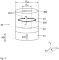
- Fig. 1 illustrates a magnetoresistive element 20, according to an embodiment.
- the magnetoresistive element 20 can comprise a magnetic tunnel junction.
- the magnetoresistive element 20 can comprise a reference layer 21 having a fixed reference magnetization 210, a sense layer 23 having a free sense magnetization 230 and a tunnel barrier layer 22 between the reference layer 21 and the sense layer 23.
- the sense magnetization 230 comprises a vortex configuration substantially parallel to the plane of the sense layer 23 in the absence of an external magnetic field 60.
- the reference layer 21, tunnel barrier layer 22 and sense layer 23 are stacked perpendicular to a layer plane P L in which the layers 21, 22, 23 extend.
- the reference layer 21 has a perpendicular magnetic anisotropy (PMA) such that the reference magnetization 210 is oriented substantially perpendicular to the layer plane P L .
- PMA perpendicular magnetic anisotropy
- the magnetoresistive element 20 has an annular cross-section in the layer plane P L .
- the portion of the magnetoresistive element 20 thus has an interior part 201 and an exterior part 202.
- the interior part 201 can be void or comprise an insulating material.
- the magnetoresistive element 20 has an inner diameter D int and outer diameter D out .
- the portion comprises the sense layer 23. In this configuration, the tunnel barrier 22 and the reference layer 21 do not have an annular cross-section.
- the interior part 201 extending only along the sense layer 23 thickness is shown in Fig. 1 by the dashed line.
- the sense magnetization 230 Due to the annular shape of the sense layer 23, the sense magnetization 230 has a closed flux path configuration that is orientable either in the clockwise or counterclockwise direction.
- the closed flux path configuration of the sense magnetization 230 can be considered having a vortex configuration without vortex core.
- the sense magnetization 230 has a magnetic vector having a fixed orthogonal direction z that is substantially perpendicular to the layer plane P L .
- the closed flux path configuration of the sense magnetization 230 can measure a Z-axis component of an external magnetic field, i.e., a component perpendicular to the layer plane P L .
- the magnetoresistive element 20 has an OOP sensitivity axis.
- the magnetic vector of the sense magnetization 230 varies in a first orthogonal direction +z or a second orthogonal direction -z, opposed to the first orthogonal direction +z, depending on the direction and magnitude of the external magnetic field 60 that is substantially perpendicular to the layer plane P L .
- the portion of the magnetoresistive element 20 further comprises the sense layer 23 and the reference layer 23.
- the reference layer 21 does not have an annular cross-section.
- the portion of the magnetoresistive element 20 can comprise the sense layer 23, the tunnel barrier layer 22 and the reference layer 21.
- the performances of the magnetoresistive element 20 depend on its geometry and more particularly, the inner diameter D int , the outer diameter D out , and the thickness of the magnetoresistive element 20.
- Fig. 2 reports the field dependence of the magnetoresistance MRH, measured on the magnetoresistive element 20 for different inner and outer diameters D int , D out . More particularly, Fig. 2 reports the magnetic sensitivity as a function of the ratio of the inner diameter D int to the outer diameter D out . It can be seen that the magnetic sensitivity increases when the ratio of the inner diameter D int to the outer diameter D out is greater than 0.6.
- electrical short circuit can be observed in the magnetoresistive element 20 (between the reference layer and the sense layer) when the inner diameter D int is smaller than 300 nm.
- the outer diameter D out is between 500 nm and 5000 nm.
- the inner diameter D int is larger than 300 nm and the difference between the inner and outer diameters D int , D out is greater than 150 nm.
- the outer diameter D out equal or smaller the 5000 nm ensures that the sense magnetization 230 has a vortex configuration in the absence of an external magnetic field.
- the aspect ratio of the thickness to diameter of the sense layer 23 can be between 0,005 and 2.
- the aspect ratio between 0,005 and 2 also ensures that the sense magnetization 230 has a vortex configuration in the absence of an external magnetic field.
- the resistance-area-product RA of the magnetoresistive element 20 can be higher than 50 ohm ⁇ m 2 .
- Figs. 3a to 3c show different possible geometries of the magnetoresistive element 20 within the scope of the disclosure. More particularly, Fig. 3a shows the magnetoresistive element 20 where the interior part 201 has a substantially circular shape. Fig. 3a shows the magnetoresistive element 20 where the interior part 201 has an elliptical shape. In the geometries of Figs 3a and 3b , the interior part 201 is substantially concentric with the exterior part 202. Fig. 3c shows the magnetoresistive element 20 where the interior part 201 is nonconcentric with the exterior part 202.
- the reference and sense layers 21, 23 can comprise, or be formed of, a ferromagnetic material such as a cobalt ("Co"), iron ("Fe") or nickel (“Ni”) based alloy and preferentially a CoFe, NiFe or CoFeB based alloy.
- the sense layer 21 should have a thickness that is greater than 15 nm.
- the reference and sense layers 21, 23 can comprise a multilayer structure where each layer can include a ferromagnetic material such as a Co, Fe or Ni based alloy and preferentially a CoFe, NiFe or CoFeB based alloy, and nonmagnetic layers such as Ta, Ti, W, Ru, Ir.
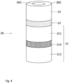
- the reference layer 21 can comprise a synthetic antiferromagnetic (SAF) structure including a first reference sublayer 211 in contact with the tunnel barrier layer 22 and a second reference sublayer 212 separated from the first reference sublayer 211 by a coupling layer 213, wherein the coupling layer 213 antiferromagnetically couple the first reference sublayer 211 to the second reference sublayer 212.
- SAF synthetic antiferromagnetic
- Each of the first and second reference sublayer 211, 212 has a PMA such that a reference magnetization 210 is oriented substantially perpendicular to the plane of the first and second reference sublayer 211, 212 and in opposite directions.
- the sense layer 23 comprises a SAF sense layer.
- the sense layer 23 comprises a first sense ferromagnetic layer having a first sense magnetization, and a second sense ferromagnetic layer having a second sense magnetization.
- the magnetization of the two sense ferromagnetic layers can be coupled in an anti-parallel direction due to the presence of an anti-parallel coupling layer.
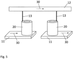
- Fig. 5 illustrates a magnetoresistive sensor device 10 comprising a plurality of the magnetoresistive elements 20, according to an embodiment.
- Fig. 3 shows only two magnetoresistive elements 20 but it should be understood that the magnetoresistive sensor device 10 can comprises more the two magnetoresistive elements 20.
- the magnetoresistive elements 20 can be electrically connected in series or in parallel. In the example of Fig. 3 , the magnetoresistive elements 20 are electrically connected in series. In particular, one end of the magnetoresistive element 20 is connected to a first electrical connector 11 and the other end of the magnetoresistive element 20 is connected to a second electrical connector 12, for example through a via 13.
- the magnitude of the external magnetic field 60 in the +z, -z direction can be measured by passing a sense current 30 in the magnetoresistive elements 20 of the magnetoresistive sensor device 10, through the first and second electrical connectors 11, 12 and the vias 13.
- the magnitude of the sense current 30 varies with the conductance (or resistance) of the magnetoresistive elements 20. The latter depends on the relative orientation of the sense magnetization 210 relative to the orientation of the reference magnetization 230 (see Fig. 1 ).
Landscapes
- Physics & Mathematics (AREA)
- Engineering & Computer Science (AREA)
- Chemical & Material Sciences (AREA)
- Crystallography & Structural Chemistry (AREA)
- Power Engineering (AREA)
- Condensed Matter Physics & Semiconductors (AREA)
- General Physics & Mathematics (AREA)
- Manufacturing & Machinery (AREA)
- Hall/Mr Elements (AREA)
- Measuring Magnetic Variables (AREA)
Abstract
Description
- The present invention concerns a magnetoresistive element comprising a sense layer, for measuring an external magnetic field along an axis substantially perpendicular to the plane of the sense layer.
- Magnetic sensors are widely used in cell phones and other mobile devices as electronic compass. For a two-dimensional external magnetic field in an X-Y plane, measurement of the X and Y components of the external magnetic field within the plane may be implemented by using two orthogonal sensors. For the measurement on the external magnetic field in a Z-axis direction, a separate single-axis planar magnetoresistive sensor arranged perpendicular to a two-axis planar sensor can be used. This solution requires assembling two different sensors, the X-Y two-axis magnetoresistive sensor and the Z-axis magnetoresistive sensor.
- The external magnetic field in a Z-axis direction canal can further be measured by using a flux guide to convert an external magnetic field from the Z-axis direction into magnetic field components in the X- and Y-axis directions. For example, document
US2012206137 discloses a singlechip three-axis AMR sensor, which implements measurement of an external magnetic field in the Z-axis direction by placing a flux guide above in-plane sensors. In such solution, the external magnetic field in the Z-axis direction is not fully converted into the X- and Y-axis directions. Moreover, such sensor design needs to use a specific algorithm for calculating the external magnetic field in the Z-axis direction, which makes the sensor design more complicated. - Another solution for measuring an external magnetic field in a Z-axis direction includes using magnetic materials with perpendicular magnetic anisotropy. For example, document
US20130168787 discloses a magnetic sensor which measures a Z-axis component of an external magnetic field by using a perpendicular magnetic anisotropy material. - In the European Patent Application No.
EP4012431 , the present applicant discloses a magnetoresistive element for measuring a Z-axis component of an external magnetic field (or having an out-of-plane (OOP) sensitivity axis). The magnetoresistive element comprises a reference layer having a reference magnetization that is fixed and oriented substantially perpendicular to the plane of the reference layer. The magnetoresistive element further comprises a tunnel barrier layer and a sense layer having a free sense magnetization that has a vortex configuration in the absence of an external magnetic field. The vortex configuration is substantially parallel to the plane of the sense layer and has a vortex core magnetization direction along an out-of-plane axis substantially perpendicular to the plane of the sense layer. - However, the magnetoresistive element having an OOP sensitivity axis shows a non-negligible hysteresis that originates from the vortex core polarity switching which happens at high fields. The magnitude of the hysteresis and the vortex core switching field depends on the size of the vortex core, the geometry of the magnetoresistive element, and the magnetic material constituting the sensing layer. The magnitude of the hysteresis can reach 5 to 10 mT. The magnitude of the hysteresis can increase after the magnetoresistive element has been exposed to a high magnetic field (above the vortex core switching field). Consequently, the magnetoresistive element may have poor accuracy, reproducibility, and repeatability in operation.
- Moreover, in the magnetoresistive element with the sense magnetization comprising a vortex configuration, different conductivity levels for different vortex core polarities may occur. In the case the reference layer comprises a synthetic antiferromagnet (SAF), the different core polarities will induce different conductivity levels. A larger or smaller conductivity of the magnetoresistive element is obtained when the vortex core and the reference magnetization are, respectively, in the same or opposite directions. A temperature increase results in a decrease in the core polarity switching field which, in turn, leads to a hysteresis appearing at smaller field exposure. This results in a reduced working range of the magnetoresistive element. In order to obtain a good accuracy and reproducibility of the electric response provided by the magnetoresistive element, the latter should be used in external magnetic fields that are below the vortex core switching field.
- The present disclosure concerns a magnetoresistive element for sensing an external magnetic field, comprising a tunnel barrier layer sandwiched between a ferromagnetic reference layer having a pinned reference magnetization, and a ferromagnetic sense layer having a sense magnetization that can be freely oriented in the external magnetic field. The reference, tunnel barrier, and sense layers are stacked perpendicular to a layer plane thereof. The reference magnetization is oriented substantially perpendicular to the layer plane, and the sense magnetization is oriented substantially parallel to the layer plane. At least a portion of the magnetoresistive element has an annular cross-section in the layer plane forming an interior part and an exterior part of said at least a portion, the interior part having an inner diameter and the exterior part having an outer diameter. Said at least a portion comprises the sense layer, the sense magnetization having a closed flux path configuration being orientable either in the clockwise or counterclockwise direction. The inner diameter is larger than 300 nm, and a difference between the inner and outer diameters is greater than 150 nm.
- The present disclosure further concerns a magnetoresistive sensor device comprising a plurality of the magnetoresistive elements, wherein the magnetoresistive elements are electrically connected in series or in parallel.
- The magnetoresistive element disclosed herein has no hysteresis. The magnetoresistive element can work in external magnetic fields above the vortex core switching field, thus has an extended magnetic field measuring working range.
- Exemplar embodiments are disclosed in the description and illustrated by the drawings in which:
-
Fig. 1 illustrates a magnetoresistive element comprising a reference layer, a tunnel barrier layer, and a sense layer, and having an annular cross-section with an inner diameter and outer diameter, according to an embodiment; -
Fig. 2 reports the magnetic sensitivity as a function of the ratio of the inner diameter to the outer diameter of the magnetoresistive element; -
Figs. 3a-3c show different possible geometries of the magnetoresistive element, according to possible embodiments; -
Fig. 4 shows the reference layer of the magnetoresistive element, according to an embodiment; and -
Fig. 5 illustrates a magnetoresistive sensor device comprising a plurality of the magnetoresistive elements, according to an embodiment. -
Fig. 1 illustrates amagnetoresistive element 20, according to an embodiment. Themagnetoresistive element 20 can comprise a magnetic tunnel junction. In particular, themagnetoresistive element 20 can comprise areference layer 21 having a fixed reference magnetization 210, asense layer 23 having afree sense magnetization 230 and atunnel barrier layer 22 between thereference layer 21 and thesense layer 23. Thesense magnetization 230 comprises a vortex configuration substantially parallel to the plane of thesense layer 23 in the absence of an externalmagnetic field 60. - As shown in
Fig. 1 , thereference layer 21,tunnel barrier layer 22 andsense layer 23 are stacked perpendicular to a layer plane PL in which thelayers reference layer 21 has a perpendicular magnetic anisotropy (PMA) such that the reference magnetization 210 is oriented substantially perpendicular to the layer plane PL. - In an embodiment, at least a portion of the
magnetoresistive element 20 has an annular cross-section in the layer plane PL. The portion of themagnetoresistive element 20 thus has aninterior part 201 and anexterior part 202. Theinterior part 201 can be void or comprise an insulating material. Themagnetoresistive element 20 has an inner diameter Dint and outer diameter Dout. In one aspect, the portion comprises thesense layer 23. In this configuration, thetunnel barrier 22 and thereference layer 21 do not have an annular cross-section. Theinterior part 201 extending only along thesense layer 23 thickness is shown inFig. 1 by the dashed line. Due to the annular shape of thesense layer 23, thesense magnetization 230 has a closed flux path configuration that is orientable either in the clockwise or counterclockwise direction. The closed flux path configuration of thesense magnetization 230 can be considered having a vortex configuration without vortex core. - Preferably, the
sense magnetization 230 has a magnetic vector having a fixed orthogonal direction z that is substantially perpendicular to the layer plane PL. Thus, the closed flux path configuration of thesense magnetization 230 can measure a Z-axis component of an external magnetic field, i.e., a component perpendicular to the layer plane PL. In other words, themagnetoresistive element 20 has an OOP sensitivity axis. In normal operation of themagnetoresistive element 20, the magnetic vector of thesense magnetization 230 varies in a first orthogonal direction +z or a second orthogonal direction -z, opposed to the first orthogonal direction +z, depending on the direction and magnitude of the externalmagnetic field 60 that is substantially perpendicular to the layer plane PL. - In one aspect, the portion of the
magnetoresistive element 20 further comprises thesense layer 23 and thereference layer 23. In this configuration, thereference layer 21 does not have an annular cross-section. In another aspect, the portion of themagnetoresistive element 20 can comprise thesense layer 23, thetunnel barrier layer 22 and thereference layer 21. - The performances of the
magnetoresistive element 20 depend on its geometry and more particularly, the inner diameter Dint, the outer diameter Dout, and the thickness of themagnetoresistive element 20. -
Fig. 2 reports the field dependence of the magnetoresistance MRH, measured on themagnetoresistive element 20 for different inner and outer diameters Dint, Dout. More particularly,Fig. 2 reports the magnetic sensitivity as a function of the ratio of the inner diameter Dint to the outer diameter Dout. It can be seen that the magnetic sensitivity increases when the ratio of the inner diameter Dint to the outer diameter Dout is greater than 0.6. - Moreover, electrical short circuit can be observed in the magnetoresistive element 20 (between the reference layer and the sense layer) when the inner diameter Dint is smaller than 300 nm.
- It has been found that that optimum performances of the
magnetoresistive element 20 are obtained when the inner diameter Dint is larger than 300 nm, and a difference between the inner and outer diameters Dint, Dout is greater than 150 nm. - In one aspect, the outer diameter Dout is between 500 nm and 5000 nm. The inner diameter Dint is larger than 300 nm and the difference between the inner and outer diameters Dint, Dout is greater than 150 nm. The outer diameter Dout equal or smaller the 5000 nm ensures that the
sense magnetization 230 has a vortex configuration in the absence of an external magnetic field. - In another aspect, the aspect ratio of the thickness to diameter of the
sense layer 23 can be between 0,005 and 2. The aspect ratio between 0,005 and 2 also ensures that thesense magnetization 230 has a vortex configuration in the absence of an external magnetic field. - In some embodiments, the resistance-area-product RA of the
magnetoresistive element 20 can be higher than 50 ohm·µm2. -
Figs. 3a to 3c show different possible geometries of themagnetoresistive element 20 within the scope of the disclosure. More particularly,Fig. 3a shows themagnetoresistive element 20 where theinterior part 201 has a substantially circular shape.Fig. 3a shows themagnetoresistive element 20 where theinterior part 201 has an elliptical shape. In the geometries ofFigs 3a and 3b , theinterior part 201 is substantially concentric with theexterior part 202.Fig. 3c shows themagnetoresistive element 20 where theinterior part 201 is nonconcentric with theexterior part 202. - The reference and sense layers 21, 23 can comprise, or be formed of, a ferromagnetic material such as a cobalt ("Co"), iron ("Fe") or nickel ("Ni") based alloy and preferentially a CoFe, NiFe or CoFeB based alloy. The
sense layer 21 should have a thickness that is greater than 15 nm. The reference and sense layers 21, 23 can comprise a multilayer structure where each layer can include a ferromagnetic material such as a Co, Fe or Ni based alloy and preferentially a CoFe, NiFe or CoFeB based alloy, and nonmagnetic layers such as Ta, Ti, W, Ru, Ir. - In a possible configuration of the
magnetoresistive element 20 shown inFig. 4 , thereference layer 21 can comprise a synthetic antiferromagnetic (SAF) structure including afirst reference sublayer 211 in contact with thetunnel barrier layer 22 and asecond reference sublayer 212 separated from thefirst reference sublayer 211 by acoupling layer 213, wherein thecoupling layer 213 antiferromagnetically couple thefirst reference sublayer 211 to thesecond reference sublayer 212. Each of the first andsecond reference sublayer second reference sublayer - In some embodiments not represented, the
sense layer 23 comprises a SAF sense layer. In particular, thesense layer 23 comprises a first sense ferromagnetic layer having a first sense magnetization, and a second sense ferromagnetic layer having a second sense magnetization. The magnetization of the two sense ferromagnetic layers can be coupled in an anti-parallel direction due to the presence of an anti-parallel coupling layer. -
Fig. 5 illustrates amagnetoresistive sensor device 10 comprising a plurality of themagnetoresistive elements 20, according to an embodiment.Fig. 3 shows only twomagnetoresistive elements 20 but it should be understood that themagnetoresistive sensor device 10 can comprises more the twomagnetoresistive elements 20. Themagnetoresistive elements 20 can be electrically connected in series or in parallel. In the example ofFig. 3 , themagnetoresistive elements 20 are electrically connected in series. In particular, one end of themagnetoresistive element 20 is connected to a firstelectrical connector 11 and the other end of themagnetoresistive element 20 is connected to a secondelectrical connector 12, for example through a via 13. - The magnitude of the external
magnetic field 60 in the +z, -z direction can be measured by passing a sense current 30 in themagnetoresistive elements 20 of themagnetoresistive sensor device 10, through the first and secondelectrical connectors vias 13. The magnitude of the sense current 30 varies with the conductance (or resistance) of themagnetoresistive elements 20. The latter depends on the relative orientation of the sense magnetization 210 relative to the orientation of the reference magnetization 230 (seeFig. 1 ). -
- 10
- magnetoresistive sensor device
- 11
- first electrical connector
- 12
- second electrical connector
- 13
- via
- 2
- magnetoresistive sensor element
- 20
- magnetic tunnel junction
- 201
- interior part
- 202
- exterior part
- 21
- reference layer
- 210
- reference magnetization
- 211
- first reference sublayer
- 212
- second reference sublayer
- 213
- coupling layer
- 22
- tunnel barrier layer
- 23
- sense layer
- 230
- sense magnetization
- 30
- sense current
- 60
- external magnetic field
- Dint
- inner diameter
- Dout
- outer diameter
- PL
- layer plane
- z
- orthogonal direction
- +z
- first orthogonal direction
- -z
- second orthogonal direction
Claims (11)
- Magnetoresistive element for sensing an external magnetic field, comprising:a tunnel barrier layer (22) sandwiched between a ferromagnetic reference layer (21) having a pinned reference magnetization (210), and a ferromagnetic sense layer (23) having a sense magnetization (230) that can be freely oriented in the external magnetic field (60);wherein the reference, tunnel barrier, and sense layers (21, 22, 23) are stacked perpendicular to a layer plane (PL) thereof;wherein the reference magnetization (210) is oriented substantially perpendicular to the layer plane (PL), and the sense magnetization (230) is oriented substantially parallel to the layer plane (PL);characterized in thatat least a portion of the magnetoresistive element (20) has an annular cross-section in the layer plane (PL) forming an interior part (201) and an exterior part (202) of said at least a portion , the interior part (201) having an inner diameter (Dint) and the exterior part (202) having an outer diameter (Dout);wherein said at least a portion comprises the sense layer (23), and wherein the sense magnetization (230) has a closed flux path configuration being orientable either in the clockwise or counterclockwise direction; andwherein the inner diameter (Dint) being larger than 300 nm, and a difference between the inner and outer diameters (Dint, Dout) is greater than 150 nm.
- Magnetoresistive element according to claim 1,
wherein said at least a portion further comprises the reference layer (23). - Magnetoresistive element according to claim 1 or 2,
wherein said at least a portion further comprises the tunnel barrier layer (22). - Magnetoresistive element according to any one of claims 1 or 3,
wherein the outer diameter (Dout) is between 500 nm and 5000 nm. - Magnetoresistive element according to any one of claims 1 or 4,
wherein the sense layer (23) has a thickness greater than 15 nm. - Magnetoresistive element according to any one of claims 1 or 5,
wherein the aspect ratio of the thickness to diameter of the sense layer (23) is between 0,005 and 2. - Magnetoresistive element according to any one of claims 1 or 6,
wherein the resistance-area-product (RA) of the magnetoresistive element (20) is higher than 50 ohm·µm2. - Magnetoresistive element according to any one of claims 1 or 7,
wherein the interior part (201) has a substantially circular shape. - Magnetoresistive element according to any one of claims 1 or 7,
wherein the interior part (201) has a substantially elliptical shape. - Magnetoresistive element according to any one of claims 1 or 9,
wherein the interior part (201) is nonconcentric with the exterior part (202). - Magnetoresistive sensor device comprising a plurality of the magnetoresistive elements according to any one of claims 1 or 10, wherein the magnetoresistive elements are electrically connected in series or in parallel.
Priority Applications (3)
| Application Number | Priority Date | Filing Date | Title |
|---|---|---|---|
| EP23315034.1A EP4417989B1 (en) | 2023-02-17 | 2023-02-17 | Magnetoresistive element having an out-of-plane sensitivity axis and having reduced hysteresis and increased working field range |
| PCT/IB2024/051324 WO2024171048A1 (en) | 2023-02-17 | 2024-02-13 | Magnetoresistive element having an out-of-plane sensitivity axis and having reduced hysteresis and increased working field range |
| TW113105498A TW202509515A (en) | 2023-02-17 | 2024-02-16 | Magnetoresistive element having an out-of-plane sensitivity axis and having reduced hysteresis and increased working field range |
Applications Claiming Priority (1)
| Application Number | Priority Date | Filing Date | Title |
|---|---|---|---|
| EP23315034.1A EP4417989B1 (en) | 2023-02-17 | 2023-02-17 | Magnetoresistive element having an out-of-plane sensitivity axis and having reduced hysteresis and increased working field range |
Publications (2)
| Publication Number | Publication Date |
|---|---|
| EP4417989A1 true EP4417989A1 (en) | 2024-08-21 |
| EP4417989B1 EP4417989B1 (en) | 2025-07-23 |
Family
ID=85601602
Family Applications (1)
| Application Number | Title | Priority Date | Filing Date |
|---|---|---|---|
| EP23315034.1A Active EP4417989B1 (en) | 2023-02-17 | 2023-02-17 | Magnetoresistive element having an out-of-plane sensitivity axis and having reduced hysteresis and increased working field range |
Country Status (3)
| Country | Link |
|---|---|
| EP (1) | EP4417989B1 (en) |
| TW (1) | TW202509515A (en) |
| WO (1) | WO2024171048A1 (en) |
Cited By (1)
| Publication number | Priority date | Publication date | Assignee | Title |
|---|---|---|---|---|
| EP4468849A1 (en) * | 2023-05-24 | 2024-11-27 | Allegro MicroSystems, LLC | Magnetoresistive element and magnetic switch comprising the magnetoresistive element |
Citations (6)
| Publication number | Priority date | Publication date | Assignee | Title |
|---|---|---|---|---|
| KR20090063625A (en) * | 2007-12-14 | 2009-06-18 | 한국전자통신연구원 | Magnetic field detection device |
| US20120206137A1 (en) | 2011-02-14 | 2012-08-16 | Memsic, Inc. | Monolithic tri-axis amr sensor and manufacturing method thereof |
| US20130168787A1 (en) | 2011-12-28 | 2013-07-04 | Industrial Technology Research Institute | Magnetic sensor |
| CN203932116U (en) * | 2014-05-27 | 2014-11-05 | 中国科学院物理研究所 | Close-shaped MTJ |
| US20170236570A1 (en) * | 2007-10-31 | 2017-08-17 | New York University | Current induced spin-momentum transfer stack with dual insulating layers |
| EP4012431A1 (en) | 2020-12-11 | 2022-06-15 | Crocus Technology S.A. | Magnetoresistive element for sensing a magnetic field in a z-axis |
-
2023
- 2023-02-17 EP EP23315034.1A patent/EP4417989B1/en active Active
-
2024
- 2024-02-13 WO PCT/IB2024/051324 patent/WO2024171048A1/en not_active Ceased
- 2024-02-16 TW TW113105498A patent/TW202509515A/en unknown
Patent Citations (6)
| Publication number | Priority date | Publication date | Assignee | Title |
|---|---|---|---|---|
| US20170236570A1 (en) * | 2007-10-31 | 2017-08-17 | New York University | Current induced spin-momentum transfer stack with dual insulating layers |
| KR20090063625A (en) * | 2007-12-14 | 2009-06-18 | 한국전자통신연구원 | Magnetic field detection device |
| US20120206137A1 (en) | 2011-02-14 | 2012-08-16 | Memsic, Inc. | Monolithic tri-axis amr sensor and manufacturing method thereof |
| US20130168787A1 (en) | 2011-12-28 | 2013-07-04 | Industrial Technology Research Institute | Magnetic sensor |
| CN203932116U (en) * | 2014-05-27 | 2014-11-05 | 中国科学院物理研究所 | Close-shaped MTJ |
| EP4012431A1 (en) | 2020-12-11 | 2022-06-15 | Crocus Technology S.A. | Magnetoresistive element for sensing a magnetic field in a z-axis |
Cited By (1)
| Publication number | Priority date | Publication date | Assignee | Title |
|---|---|---|---|---|
| EP4468849A1 (en) * | 2023-05-24 | 2024-11-27 | Allegro MicroSystems, LLC | Magnetoresistive element and magnetic switch comprising the magnetoresistive element |
Also Published As
| Publication number | Publication date |
|---|---|
| EP4417989B1 (en) | 2025-07-23 |
| WO2024171048A1 (en) | 2024-08-22 |
| TW202509515A (en) | 2025-03-01 |
Similar Documents
| Publication | Publication Date | Title |
|---|---|---|
| US10734443B2 (en) | Dual manetoresistance element with two directions of response to external magnetic fields | |
| US11531071B2 (en) | Magnetic field detection device | |
| US10753989B2 (en) | Magnetoresistance element with perpendicular or parallel magnetic anistropy | |
| CN107976644B (en) | Magnetic field detection device | |
| US11519977B2 (en) | Stray field robust XMR sensor using perpendicular anisotropy | |
| JP5066579B2 (en) | Magnetic sensor and magnetic sensor module | |
| US9739842B2 (en) | Magnetic field sensor with skewed sense magnetization of sense layer | |
| EP3223028B1 (en) | Multiple axis magnetic sensor | |
| EP3229035B1 (en) | Magnetic field sensor with permanent magnet biasing | |
| US20250271471A1 (en) | Magnetic field detection apparatus and current detection apparatus | |
| US20230251331A1 (en) | Sensor unit | |
| CN104103753A (en) | Magnetoresistive film layer structure and magnetic field sensor using the magnetoresistive film layer structure | |
| EP3236276B1 (en) | Magnetic field sensor with multiple axis sense capability | |
| EP4417989B1 (en) | Magnetoresistive element having an out-of-plane sensitivity axis and having reduced hysteresis and increased working field range | |
| CN119165414A (en) | Spin Hall magnetoresistive sensor and electronic device including the same | |
| US20150198430A1 (en) | Magnetism detection element and rotation detector | |
| CN116243222B (en) | Magnetoresistive device, manufacturing method thereof and magnetic sensing device | |
| JP2015155796A (en) | Current sensor | |
| CN121285254A (en) | Tunnel magnetoresistance element, magnetic sensor module, and current sensor | |
| JP2014142297A (en) | Proximity sensor, and game machine |
Legal Events
| Date | Code | Title | Description |
|---|---|---|---|
| PUAI | Public reference made under article 153(3) epc to a published international application that has entered the european phase |
Free format text: ORIGINAL CODE: 0009012 |
|
| STAA | Information on the status of an ep patent application or granted ep patent |
Free format text: STATUS: THE APPLICATION HAS BEEN PUBLISHED |
|
| AK | Designated contracting states |
Kind code of ref document: A1 Designated state(s): AL AT BE BG CH CY CZ DE DK EE ES FI FR GB GR HR HU IE IS IT LI LT LU LV MC ME MK MT NL NO PL PT RO RS SE SI SK SM TR |
|
| STAA | Information on the status of an ep patent application or granted ep patent |
Free format text: STATUS: REQUEST FOR EXAMINATION WAS MADE |
|
| 17P | Request for examination filed |
Effective date: 20240919 |
|
| RBV | Designated contracting states (corrected) |
Designated state(s): AL AT BE BG CH CY CZ DE DK EE ES FI FR GB GR HR HU IE IS IT LI LT LU LV MC ME MK MT NL NO PL PT RO RS SE SI SK SM TR |
|
| GRAP | Despatch of communication of intention to grant a patent |
Free format text: ORIGINAL CODE: EPIDOSNIGR1 |
|
| STAA | Information on the status of an ep patent application or granted ep patent |
Free format text: STATUS: GRANT OF PATENT IS INTENDED |
|
| RIC1 | Information provided on ipc code assigned before grant |
Ipc: H01F 10/32 20060101ALI20250124BHEP Ipc: G01R 33/00 20060101ALI20250124BHEP Ipc: G01R 33/09 20060101AFI20250124BHEP |
|
| INTG | Intention to grant announced |
Effective date: 20250217 |
|
| GRAS | Grant fee paid |
Free format text: ORIGINAL CODE: EPIDOSNIGR3 |
|
| GRAA | (expected) grant |
Free format text: ORIGINAL CODE: 0009210 |
|
| STAA | Information on the status of an ep patent application or granted ep patent |
Free format text: STATUS: THE PATENT HAS BEEN GRANTED |
|
| AK | Designated contracting states |
Kind code of ref document: B1 Designated state(s): AL AT BE BG CH CY CZ DE DK EE ES FI FR GB GR HR HU IE IS IT LI LT LU LV MC ME MK MT NL NO PL PT RO RS SE SI SK SM TR |
|
| REG | Reference to a national code |
Ref country code: GB Ref legal event code: FG4D |
|
| REG | Reference to a national code |
Ref country code: CH Ref legal event code: EP |
|
| REG | Reference to a national code |
Ref country code: DE Ref legal event code: R096 Ref document number: 602023005051 Country of ref document: DE |
|
| REG | Reference to a national code |
Ref country code: IE Ref legal event code: FG4D |
|
| REG | Reference to a national code |
Ref country code: NL Ref legal event code: MP Effective date: 20250723 |
|
| PG25 | Lapsed in a contracting state [announced via postgrant information from national office to epo] |
Ref country code: PT Free format text: LAPSE BECAUSE OF FAILURE TO SUBMIT A TRANSLATION OF THE DESCRIPTION OR TO PAY THE FEE WITHIN THE PRESCRIBED TIME-LIMIT Effective date: 20251124 |
|
| PG25 | Lapsed in a contracting state [announced via postgrant information from national office to epo] |
Ref country code: NL Free format text: LAPSE BECAUSE OF FAILURE TO SUBMIT A TRANSLATION OF THE DESCRIPTION OR TO PAY THE FEE WITHIN THE PRESCRIBED TIME-LIMIT Effective date: 20250723 |
|
| REG | Reference to a national code |
Ref country code: AT Ref legal event code: MK05 Ref document number: 1816943 Country of ref document: AT Kind code of ref document: T Effective date: 20250723 |
|
| PG25 | Lapsed in a contracting state [announced via postgrant information from national office to epo] |
Ref country code: IS Free format text: LAPSE BECAUSE OF FAILURE TO SUBMIT A TRANSLATION OF THE DESCRIPTION OR TO PAY THE FEE WITHIN THE PRESCRIBED TIME-LIMIT Effective date: 20251123 |
|
| PG25 | Lapsed in a contracting state [announced via postgrant information from national office to epo] |
Ref country code: NO Free format text: LAPSE BECAUSE OF FAILURE TO SUBMIT A TRANSLATION OF THE DESCRIPTION OR TO PAY THE FEE WITHIN THE PRESCRIBED TIME-LIMIT Effective date: 20251023 |
|
| REG | Reference to a national code |
Ref country code: LT Ref legal event code: MG9D |
|
| PG25 | Lapsed in a contracting state [announced via postgrant information from national office to epo] |
Ref country code: AT Free format text: LAPSE BECAUSE OF FAILURE TO SUBMIT A TRANSLATION OF THE DESCRIPTION OR TO PAY THE FEE WITHIN THE PRESCRIBED TIME-LIMIT Effective date: 20250723 |
|
| PG25 | Lapsed in a contracting state [announced via postgrant information from national office to epo] |
Ref country code: FI Free format text: LAPSE BECAUSE OF FAILURE TO SUBMIT A TRANSLATION OF THE DESCRIPTION OR TO PAY THE FEE WITHIN THE PRESCRIBED TIME-LIMIT Effective date: 20250723 |
|
| PG25 | Lapsed in a contracting state [announced via postgrant information from national office to epo] |
Ref country code: HR Free format text: LAPSE BECAUSE OF FAILURE TO SUBMIT A TRANSLATION OF THE DESCRIPTION OR TO PAY THE FEE WITHIN THE PRESCRIBED TIME-LIMIT Effective date: 20250723 |
|
| PG25 | Lapsed in a contracting state [announced via postgrant information from national office to epo] |
Ref country code: GR Free format text: LAPSE BECAUSE OF FAILURE TO SUBMIT A TRANSLATION OF THE DESCRIPTION OR TO PAY THE FEE WITHIN THE PRESCRIBED TIME-LIMIT Effective date: 20251024 |
|
| PG25 | Lapsed in a contracting state [announced via postgrant information from national office to epo] |
Ref country code: SE Free format text: LAPSE BECAUSE OF FAILURE TO SUBMIT A TRANSLATION OF THE DESCRIPTION OR TO PAY THE FEE WITHIN THE PRESCRIBED TIME-LIMIT Effective date: 20250723 |
|
| PG25 | Lapsed in a contracting state [announced via postgrant information from national office to epo] |
Ref country code: LV Free format text: LAPSE BECAUSE OF FAILURE TO SUBMIT A TRANSLATION OF THE DESCRIPTION OR TO PAY THE FEE WITHIN THE PRESCRIBED TIME-LIMIT Effective date: 20250723 |
|
| PG25 | Lapsed in a contracting state [announced via postgrant information from national office to epo] |
Ref country code: BG Free format text: LAPSE BECAUSE OF FAILURE TO SUBMIT A TRANSLATION OF THE DESCRIPTION OR TO PAY THE FEE WITHIN THE PRESCRIBED TIME-LIMIT Effective date: 20250723 Ref country code: PL Free format text: LAPSE BECAUSE OF FAILURE TO SUBMIT A TRANSLATION OF THE DESCRIPTION OR TO PAY THE FEE WITHIN THE PRESCRIBED TIME-LIMIT Effective date: 20250723 |
|
| PG25 | Lapsed in a contracting state [announced via postgrant information from national office to epo] |
Ref country code: RS Free format text: LAPSE BECAUSE OF FAILURE TO SUBMIT A TRANSLATION OF THE DESCRIPTION OR TO PAY THE FEE WITHIN THE PRESCRIBED TIME-LIMIT Effective date: 20251023 |
|
| PG25 | Lapsed in a contracting state [announced via postgrant information from national office to epo] |
Ref country code: ES Free format text: LAPSE BECAUSE OF FAILURE TO SUBMIT A TRANSLATION OF THE DESCRIPTION OR TO PAY THE FEE WITHIN THE PRESCRIBED TIME-LIMIT Effective date: 20250723 |
|
| PG25 | Lapsed in a contracting state [announced via postgrant information from national office to epo] |
Ref country code: SM Free format text: LAPSE BECAUSE OF FAILURE TO SUBMIT A TRANSLATION OF THE DESCRIPTION OR TO PAY THE FEE WITHIN THE PRESCRIBED TIME-LIMIT Effective date: 20250723 |
|
| PG25 | Lapsed in a contracting state [announced via postgrant information from national office to epo] |
Ref country code: DK Free format text: LAPSE BECAUSE OF FAILURE TO SUBMIT A TRANSLATION OF THE DESCRIPTION OR TO PAY THE FEE WITHIN THE PRESCRIBED TIME-LIMIT Effective date: 20250723 |
|
| PGFP | Annual fee paid to national office [announced via postgrant information from national office to epo] |
Ref country code: DE Payment date: 20260107 Year of fee payment: 4 |
|
| PG25 | Lapsed in a contracting state [announced via postgrant information from national office to epo] |
Ref country code: IT Free format text: LAPSE BECAUSE OF FAILURE TO SUBMIT A TRANSLATION OF THE DESCRIPTION OR TO PAY THE FEE WITHIN THE PRESCRIBED TIME-LIMIT Effective date: 20250723 |
|
| PG25 | Lapsed in a contracting state [announced via postgrant information from national office to epo] |
Ref country code: CZ Free format text: LAPSE BECAUSE OF FAILURE TO SUBMIT A TRANSLATION OF THE DESCRIPTION OR TO PAY THE FEE WITHIN THE PRESCRIBED TIME-LIMIT Effective date: 20250723 |
|
| PG25 | Lapsed in a contracting state [announced via postgrant information from national office to epo] |
Ref country code: SK Free format text: LAPSE BECAUSE OF FAILURE TO SUBMIT A TRANSLATION OF THE DESCRIPTION OR TO PAY THE FEE WITHIN THE PRESCRIBED TIME-LIMIT Effective date: 20250723 Ref country code: EE Free format text: LAPSE BECAUSE OF FAILURE TO SUBMIT A TRANSLATION OF THE DESCRIPTION OR TO PAY THE FEE WITHIN THE PRESCRIBED TIME-LIMIT Effective date: 20250723 |