EP4412072A1 - Electric power conversion device, and electric power conversion method - Google Patents
Electric power conversion device, and electric power conversion method Download PDFInfo
- Publication number
- EP4412072A1 EP4412072A1 EP22875445.3A EP22875445A EP4412072A1 EP 4412072 A1 EP4412072 A1 EP 4412072A1 EP 22875445 A EP22875445 A EP 22875445A EP 4412072 A1 EP4412072 A1 EP 4412072A1
- Authority
- EP
- European Patent Office
- Prior art keywords
- switching elements
- power conversion
- turn
- temperature difference
- change amount
- Prior art date
- Legal status (The legal status is an assumption and is not a legal conclusion. Google has not performed a legal analysis and makes no representation as to the accuracy of the status listed.)
- Pending
Links
Images



Classifications
-
- H—ELECTRICITY
- H02—GENERATION; CONVERSION OR DISTRIBUTION OF ELECTRIC POWER
- H02M—APPARATUS FOR CONVERSION BETWEEN AC AND AC, BETWEEN AC AND DC, OR BETWEEN DC AND DC, AND FOR USE WITH MAINS OR SIMILAR POWER SUPPLY SYSTEMS; CONVERSION OF DC OR AC INPUT POWER INTO SURGE OUTPUT POWER; CONTROL OR REGULATION THEREOF
- H02M7/00—Conversion of AC power input into DC power output; Conversion of DC power input into AC power output
- H02M7/42—Conversion of DC power input into AC power output without possibility of reversal
- H02M7/44—Conversion of DC power input into AC power output without possibility of reversal by static converters
- H02M7/48—Conversion of DC power input into AC power output without possibility of reversal by static converters using discharge tubes with control electrode or semiconductor devices with control electrode
- H02M7/493—Conversion of DC power input into AC power output without possibility of reversal by static converters using discharge tubes with control electrode or semiconductor devices with control electrode the static converters being arranged for operation in parallel
-
- H—ELECTRICITY
- H02—GENERATION; CONVERSION OR DISTRIBUTION OF ELECTRIC POWER
- H02M—APPARATUS FOR CONVERSION BETWEEN AC AND AC, BETWEEN AC AND DC, OR BETWEEN DC AND DC, AND FOR USE WITH MAINS OR SIMILAR POWER SUPPLY SYSTEMS; CONVERSION OF DC OR AC INPUT POWER INTO SURGE OUTPUT POWER; CONTROL OR REGULATION THEREOF
- H02M1/00—Details of apparatus for conversion
- H02M1/0048—Circuits or arrangements for reducing losses
- H02M1/0054—Transistor switching losses
-
- H—ELECTRICITY
- H02—GENERATION; CONVERSION OR DISTRIBUTION OF ELECTRIC POWER
- H02M—APPARATUS FOR CONVERSION BETWEEN AC AND AC, BETWEEN AC AND DC, OR BETWEEN DC AND DC, AND FOR USE WITH MAINS OR SIMILAR POWER SUPPLY SYSTEMS; CONVERSION OF DC OR AC INPUT POWER INTO SURGE OUTPUT POWER; CONTROL OR REGULATION THEREOF
- H02M1/00—Details of apparatus for conversion
- H02M1/08—Circuits specially adapted for the generation of control voltages for semiconductor devices incorporated in static converters
- H02M1/088—Circuits specially adapted for the generation of control voltages for semiconductor devices incorporated in static converters for the simultaneous control of series or parallel connected semiconductor devices
-
- H—ELECTRICITY
- H02—GENERATION; CONVERSION OR DISTRIBUTION OF ELECTRIC POWER
- H02M—APPARATUS FOR CONVERSION BETWEEN AC AND AC, BETWEEN AC AND DC, OR BETWEEN DC AND DC, AND FOR USE WITH MAINS OR SIMILAR POWER SUPPLY SYSTEMS; CONVERSION OF DC OR AC INPUT POWER INTO SURGE OUTPUT POWER; CONTROL OR REGULATION THEREOF
- H02M1/00—Details of apparatus for conversion
- H02M1/32—Means for protecting converters other than automatic disconnection
- H02M1/327—Means for protecting converters other than automatic disconnection against abnormal temperatures
-
- H—ELECTRICITY
- H02—GENERATION; CONVERSION OR DISTRIBUTION OF ELECTRIC POWER
- H02M—APPARATUS FOR CONVERSION BETWEEN AC AND AC, BETWEEN AC AND DC, OR BETWEEN DC AND DC, AND FOR USE WITH MAINS OR SIMILAR POWER SUPPLY SYSTEMS; CONVERSION OF DC OR AC INPUT POWER INTO SURGE OUTPUT POWER; CONTROL OR REGULATION THEREOF
- H02M1/00—Details of apparatus for conversion
- H02M1/38—Means for preventing simultaneous conduction of switches
-
- H—ELECTRICITY
- H02—GENERATION; CONVERSION OR DISTRIBUTION OF ELECTRIC POWER
- H02M—APPARATUS FOR CONVERSION BETWEEN AC AND AC, BETWEEN AC AND DC, OR BETWEEN DC AND DC, AND FOR USE WITH MAINS OR SIMILAR POWER SUPPLY SYSTEMS; CONVERSION OF DC OR AC INPUT POWER INTO SURGE OUTPUT POWER; CONTROL OR REGULATION THEREOF
- H02M7/00—Conversion of AC power input into DC power output; Conversion of DC power input into AC power output
- H02M7/42—Conversion of DC power input into AC power output without possibility of reversal
- H02M7/44—Conversion of DC power input into AC power output without possibility of reversal by static converters
- H02M7/48—Conversion of DC power input into AC power output without possibility of reversal by static converters using discharge tubes with control electrode or semiconductor devices with control electrode
- H02M7/53—Conversion of DC power input into AC power output without possibility of reversal by static converters using discharge tubes with control electrode or semiconductor devices with control electrode using devices of a triode or transistor type requiring continuous application of a control signal
- H02M7/537—Conversion of DC power input into AC power output without possibility of reversal by static converters using discharge tubes with control electrode or semiconductor devices with control electrode using devices of a triode or transistor type requiring continuous application of a control signal using semiconductor devices only, e.g. single switched pulse inverters
- H02M7/5387—Conversion of DC power input into AC power output without possibility of reversal by static converters using discharge tubes with control electrode or semiconductor devices with control electrode using devices of a triode or transistor type requiring continuous application of a control signal using semiconductor devices only, e.g. single switched pulse inverters in a bridge configuration
-
- H—ELECTRICITY
- H03—ELECTRONIC CIRCUITRY
- H03K—PULSE TECHNIQUE
- H03K17/00—Electronic switching or gating, i.e. not by contact-making and –breaking
- H03K17/14—Modifications for compensating variations of physical values, e.g. of temperature
-
- H—ELECTRICITY
- H03—ELECTRONIC CIRCUITRY
- H03K—PULSE TECHNIQUE
- H03K17/00—Electronic switching or gating, i.e. not by contact-making and –breaking
- H03K17/28—Modifications for introducing a time delay before switching
-
- H—ELECTRICITY
- H03—ELECTRONIC CIRCUITRY
- H03K—PULSE TECHNIQUE
- H03K17/00—Electronic switching or gating, i.e. not by contact-making and –breaking
- H03K17/08—Modifications for protecting switching circuit against overcurrent or overvoltage
- H03K2017/0806—Modifications for protecting switching circuit against overcurrent or overvoltage against excessive temperature
Definitions
- the present invention relates to a configuration of a power conversion device and control of the power conversion device, and particularly relates to a technique that is effective when applied to a large-capacity power conversion device configured by connecting a plurality of power conversion units in multiple parallel.
- a power conversion device can convert DC power into AC power or a reverse direction thereof by a switching operation of a power semiconductor element, and is applied to various fields such as elevators, railways, and automobiles.
- a power conversion system capable of outputting a large current by connecting a plurality of power conversion devices (power conversion units) in parallel.
- a power conversion system has a common drive signal supplied to a plurality of power conversion devices connected in parallel, and is driven so that the plurality of power conversion devices output equal currents.
- variations in components such as wirings and elements constituting the power conversion devices may cause variations in the output currents of the power conversion devices.
- the power semiconductor element since the power semiconductor element has characteristic variations unique to the power semiconductor element, such as a turn-on delay time, a turn-off delay time, and an on-voltage, when the power semiconductor elements are connected in parallel, a current value flowing through each power semiconductor element becomes unbalanced. Therefore, the current concentrates on some power semiconductor elements, and the switching loss and the conduction loss increase, and a temperature imbalance occurs.
- the temperature imbalance affects not only output characteristics such as an output current of the power conversion device but also reliability and life of the power conversion device.
- PTL 1 discloses "A current balance adjustment circuit comprising: an output current difference calculation circuit that outputs a difference result between an output current value and a reference value when a polarity of the output current value is positive, and outputs a difference between an absolute value of the output current value and an absolute value of the reference value when the polarity of the output current value is negative, for each of output current values of a plurality of power conversion devices connected in parallel to each other and driven on the basis of a common ON signal; and an adjustment time calculation circuit that outputs an adjustment time signal indicating a delay time amount at a rising timing or a falling timing of the common ON signal according to an output value of the output current difference calculation circuit".
- Patent Literature 1 described above is a technique for suppressing one of temperature imbalance due to delay time variation and temperature imbalance due to on-voltage variation, and effects of reduction of switching loss and conduction loss and reduction of temperature imbalance are limited.
- an object of the present invention is to provide a power conversion device and a power conversion method that suppress temperature imbalance due to delay time variation and temperature imbalance due to on-voltage variation in a power conversion device including a plurality of switching elements connected in parallel.
- Another object of the present invention is to provide a power conversion device and a power conversion method that suppress temperature imbalance due to delay time variation and temperature imbalance due to on-voltage variation in a power conversion device including a plurality of power conversion units connected in parallel.
- the present invention provides a power conversion device including: a plurality of switching elements; a temperature sensor that detects temperatures of the plurality of switching elements; a carrier frequency adjusting unit that adjusts carrier frequencies of the plurality of switching elements; a delay time adjusting unit that adjusts turn-on times or turn-off times of the plurality of switching elements; and a gate voltage adjusting unit that adjusts on-voltages of the plurality of switching elements, in which the temperature sensor detects a change amount of a temperature difference between the plurality of switching elements before and after carrier frequency adjustment by the carrier frequency adjusting unit, and the delay time adjusting unit adjusts turn-on times or turn-off times of the plurality of switching elements on a basis of the detected change amount of the temperature difference.
- the present invention is characterized by including: (a) a step of detecting a temperature difference among a plurality of switching elements at a predetermined carrier frequency; (b) a step of changing a carrier frequency after the step (a); (c) a step of detecting a temperature difference among the plurality of switching elements at a changed carrier frequency after the step (b); (d) a step of calculating a change amount between the temperature difference detected in the step (a) and the temperature difference detected in the step (c) after the step (c); and (e) a step of determining whether or not adjustment of turn-on times or turn-off times of the plurality of switching elements is necessary on the basis of the calculated change amount of the temperature difference after the step (d).
- the present invention it is possible to realize a power conversion device and a power conversion method that suppress a temperature imbalance due to a delay time variation and a temperature imbalance due to an on-voltage variation in a power conversion device including a plurality of switching elements connected in parallel.
- a power conversion device including a plurality of power conversion units connected in parallel, it is possible to realize a power conversion device and a power conversion method that suppress temperature imbalance due to delay time variation and temperature imbalance due to on-voltage variation.
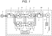
- FIG. 1 is a diagram illustrating a schematic configuration of an elevator system 1 which is an application example of a power conversion device 100 of the present embodiment.
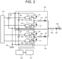
- FIG. 2 is a diagram illustrating a configuration of an inverter system 11 of FIG. 1 and a drive circuit thereof.
- the elevator system 1 of the present embodiment includes, as main components, a rope 5, a car 6, a weight 7, a motor 8, and a power conversion device 100.
- the three-phase AC power supplied from a system 2 is input to a plurality of three-phase converter systems 10 connected in parallel via a filter circuit 3, and the converter system 10 performs power conversion from AC to DC via power conversion units 12 and 13.
- a three-phase inverter system 11 in which a plurality of power conversion units 14 and 15 are connected in parallel drives the motor 8 via the filter circuit 4.
- the converter system 10 and the inverter system 11 are controlled by a control circuit unit 9.
- the inverter system 11 of FIG. 1 will be described with reference to FIG. 2 .
- the inverter system 11 includes, as main components, a plurality of (two in FIG. 2 ) power conversion units 122,123, a temperature detecting circuit 126, and a carrier frequency (switching frequency) adjusting unit 127.
- the power conversion units 122,123 are connected in parallel, input sides of the power conversion units 122,123 are connected in parallel to a converter system 10 (not illustrated), and output sides are connected to output loads 124,125 of the power conversion device 100.
- a current sensor 130 is attached to the output of the power conversion device 100.
- the power conversion unit 122 includes an upper arm switching element 110, a lower arm switching element 111, an upper arm switching freewheeling diode 114, and a lower arm switching freewheeling diode 115, and a resistor 118 and a reactor 119 are connected to an output thereof.
- delay time adjusting units 106,107 and gate voltage adjusting units 131,132 are connected to the upper arm switching element 110 and the lower arm switching element 111, respectively.
- the power conversion unit 123 includes an upper arm switching element 112, a lower arm switching element 113, an upper arm switching freewheeling diode 116, and a lower arm switching freewheeling diode 117, and a resistor 120 and a reactor 121 are connected to an output thereof.
- delay time adjusting units 108,109 and gate voltage adjusting units 133,134 are connected to the upper arm switching element 112 and the lower arm switching element 113, respectively.
- Control signals are output from an input signal 101 and input to the delay time adjusting units 106,107,108,109.
- a temperature sensor (not illustrated) is disposed on each of the upper and lower arms of the power conversion unit 122, detects the temperature of each of the upper arm switching element 110 and the lower arm switching element 111, and inputs detected temperature information to the temperature detecting circuit 126.
- temperature sensors are arranged in the upper and lower arms of the power conversion unit 123, respectively, to detect the temperatures of the upper arm switching element 112 and the lower arm switching element 113, and input detected temperature information to the temperature detecting circuit 126.
- a carrier frequency adjusting unit 127, the delay time adjusting units 106 to 109, and the gate voltage adjusting units 131 to 134 are adjusted via the temperature detecting circuit 126.
- FIG. 3 is an operation waveform when a variation in turn-on delay time occurs in the switching element.
- the horizontal axis represents time [s]
- the vertical axis represents the gate signal of the switching element 110, the gate signal of the switching element 112, the output voltage of the power conversion unit 122, the output voltage of the power conversion unit 123, the output current of the power conversion unit 122, the output current of the power conversion unit 123, the temperature of the power conversion unit 122, and the temperature of the power conversion unit 123 in order from the top.
- the pulse width of the output voltage of the power conversion unit 123 becomes narrower than that of the power conversion unit 122.
- the time during which a voltage is applied to the resistor 118 and the reactor 119 of the power conversion unit 122 becomes longer than the time during which a voltage is applied to the resistor 120 and the reactor 121 of the power conversion unit 123, and the output current of the power conversion unit 122 becomes larger than that of the power conversion unit 123.
- the current flowing through the switching element 110 of the power conversion unit 122 becomes larger than the current flowing through the switching element 112 of the power conversion unit 123. Since the switching element has an on-resistance, the larger the flowing current, the larger the heat generation, and the temperature of the power conversion unit 122 becomes larger than that of the power conversion unit 123.
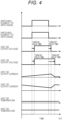
- FIG. 4 is an operation waveform when a variation in turn-off delay time occurs in the switching element.
- the pulse width of the output voltage of the power conversion unit 122 becomes narrower than that of the unit 123.
- the time during which a voltage is applied to the resistor 118 and the reactor 119 of the power conversion unit 122 becomes shorter than the time during which a voltage is applied to the resistor 120 and the reactor 121 of the power conversion unit 123, and the output current of the power conversion unit 122 becomes smaller than that of the power conversion unit 123.
- the current flowing through the switching element 110 of the power conversion unit 122 becomes smaller than the current flowing through the switching element 112 of the power conversion unit 123. Since the switching element has an on-resistance, the larger the flowing current, the larger the heat generation, and the temperature of the power conversion unit 122 becomes smaller than that of the power conversion unit 123.
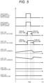
- FIG. 5 is an operation waveform when a variation in turn-off delay time occurs and the carrier frequency is low.
- the time during which a voltage is applied to the resistor 118 and the reactor 119 of the power conversion unit 122 is shorter than the time during which a voltage is applied to the resistor 120 and the reactor 121 of the unit 123.
- the number of pulses of the output voltage per second also decreases, and the difference between the time during which the voltage is applied to the resistor 118 and the reactor 119 of the power conversion unit 122 and the time during which the voltage is applied to the resistor 120 and the reactor 121 of the unit 123 becomes shorter than the time when the number of pulses is large.
- the temperature imbalance becomes smaller than that when the carrier frequency is high and the number of pulses is large.
- the difference in pulse width becomes the current imbalance, the current imbalance decreases when the carrier frequency is low also in the turn-on delay.
- FIG. 6 is an operation waveform when a variation in turn-off delay time occurs and the carrier frequency is high.
- the time during which a voltage is applied to the resistor 118 and the reactor 119 of the power conversion unit 122 is shorter than the time during which a voltage is applied to the resistor 120 and the reactor 121 of the unit 123.
- the carrier frequency When the carrier frequency is high, the number of pulses of the output voltage per second increases, and the difference between the time during which the voltage is applied to the resistor 118 and the reactor 119 of the power conversion unit 122 and the time during which the voltage is applied to the resistor 120 and the reactor 121 of the power conversion unit 123 is longer than the time when the number of pulses is small.
- the temperature imbalance becomes larger than that when the carrier frequency is low and the number of pulses is small.
- the difference in pulse width becomes the current imbalance, the current imbalance increases when the carrier frequency is high also in the turn-on delay.
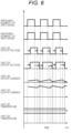
- FIG. 7 is an operation waveform when on-voltage variation occurs in the switching element.
- FIG. 8 illustrates a gate voltage dependency of the collector current characteristic with respect to the collector-emitter voltage of the switching element.
- the collector-emitter voltage is lower than that when the gate voltage is low.
- the on-voltage of the switching element can be adjusted by changing the voltage applied to the gate by each of the gate voltage adjusting units 131 to 134.
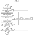
- a temperature imbalance reduction method according to the present embodiment will be described with reference to FIG. 9 .
- step S301 adjustment is started during the DC current output mode.
- the DC current output mode corresponds to the activation compensation mode of the elevator system 1 illustrated in FIG. 1 .
- step S302 a temperature difference between the plurality of switching elements (power semiconductor elements) is detected at a carrier frequency of 8 kHz, for example.
- step S303 the carrier frequency is changed, and in step S304, the temperature difference between the plurality of switching elements (power semiconductor elements) is detected again at the carrier frequency of 4 kHz, for example.
- step S305 a change amount is calculated from the temperature difference before and after the change.
- step S306 it is determined whether or not the change amount is equal to or less than a specified value.
- step S306 determines that the change amount is larger than the specified value (No)
- the process proceeds to step S307, the delay times of the switching elements 110 to 113 are adjusted by the delay time adjusting units 106 to 109, respectively, and then the process proceeds to step S302.
- the cross current due to the delay time is suppressed by repeating steps S302 to S307 until the change amount becomes equal to or less than the specified value.
- step S308 it is determined whether or not the temperature difference is equal to or less than a specified value.
- step S308 In a case where it is determined in step S308 that the temperature difference is equal to or less than the specified value (Yes), the process ends.
- step S309 the gate voltage adjusting units 131 to 134 adjust the gate voltages of the switching elements 110 to 113.
- the process returns to step S302 again, and the temperature difference is suppressed by repeating steps S302 to S309.
- the delay time and the gate voltage can be appropriately adjusted, and the temperature imbalance can be minimized.
- the present invention is not limited to the above-described embodiments, and includes various modifications.
- the above-described embodiments have been described in detail in order to explain the present invention in an easy-to-understand manner, and are not necessarily limited to those having all the described configurations.
- a part of the configuration of a certain embodiment can be replaced with the configuration of another embodiment, and the configuration of another embodiment can be added to the configuration of a certain embodiment.
Landscapes
- Engineering & Computer Science (AREA)
- Power Engineering (AREA)
- Inverter Devices (AREA)
Abstract
Description
- The present invention relates to a configuration of a power conversion device and control of the power conversion device, and particularly relates to a technique that is effective when applied to a large-capacity power conversion device configured by connecting a plurality of power conversion units in multiple parallel.
- A power conversion device can convert DC power into AC power or a reverse direction thereof by a switching operation of a power semiconductor element, and is applied to various fields such as elevators, railways, and automobiles.
- In order to respond to various applications, it has been proposed to use a power conversion system capable of outputting a large current by connecting a plurality of power conversion devices (power conversion units) in parallel. For example, such a power conversion system has a common drive signal supplied to a plurality of power conversion devices connected in parallel, and is driven so that the plurality of power conversion devices output equal currents. However, variations in components such as wirings and elements constituting the power conversion devices may cause variations in the output currents of the power conversion devices.
- For example, since the power semiconductor element has characteristic variations unique to the power semiconductor element, such as a turn-on delay time, a turn-off delay time, and an on-voltage, when the power semiconductor elements are connected in parallel, a current value flowing through each power semiconductor element becomes unbalanced. Therefore, the current concentrates on some power semiconductor elements, and the switching loss and the conduction loss increase, and a temperature imbalance occurs. The temperature imbalance affects not only output characteristics such as an output current of the power conversion device but also reliability and life of the power conversion device.
- Conventionally, when power semiconductor elements are connected in parallel, it is necessary to design the power semiconductor elements with a current value smaller than the rated current of each of the power semiconductor elements in consideration of such unbalance. Therefore, the performance of the power semiconductor element cannot be utilized to the maximum.
- Therefore,
PTL 1 discloses "A current balance adjustment circuit comprising: an output current difference calculation circuit that outputs a difference result between an output current value and a reference value when a polarity of the output current value is positive, and outputs a difference between an absolute value of the output current value and an absolute value of the reference value when the polarity of the output current value is negative, for each of output current values of a plurality of power conversion devices connected in parallel to each other and driven on the basis of a common ON signal; and an adjustment time calculation circuit that outputs an adjustment time signal indicating a delay time amount at a rising timing or a falling timing of the common ON signal according to an output value of the output current difference calculation circuit". - PTL 1:
JP 2018-153087 A -
Patent Literature 1 described above is a technique for suppressing one of temperature imbalance due to delay time variation and temperature imbalance due to on-voltage variation, and effects of reduction of switching loss and conduction loss and reduction of temperature imbalance are limited. - Therefore, an object of the present invention is to provide a power conversion device and a power conversion method that suppress temperature imbalance due to delay time variation and temperature imbalance due to on-voltage variation in a power conversion device including a plurality of switching elements connected in parallel.
- Another object of the present invention is to provide a power conversion device and a power conversion method that suppress temperature imbalance due to delay time variation and temperature imbalance due to on-voltage variation in a power conversion device including a plurality of power conversion units connected in parallel.
- In order to solve the above problems, the present invention provides a power conversion device including: a plurality of switching elements; a temperature sensor that detects temperatures of the plurality of switching elements; a carrier frequency adjusting unit that adjusts carrier frequencies of the plurality of switching elements; a delay time adjusting unit that adjusts turn-on times or turn-off times of the plurality of switching elements; and a gate voltage adjusting unit that adjusts on-voltages of the plurality of switching elements, in which the temperature sensor detects a change amount of a temperature difference between the plurality of switching elements before and after carrier frequency adjustment by the carrier frequency adjusting unit, and the delay time adjusting unit adjusts turn-on times or turn-off times of the plurality of switching elements on a basis of the detected change amount of the temperature difference.
- Further, the present invention is characterized by including: (a) a step of detecting a temperature difference among a plurality of switching elements at a predetermined carrier frequency; (b) a step of changing a carrier frequency after the step (a); (c) a step of detecting a temperature difference among the plurality of switching elements at a changed carrier frequency after the step (b); (d) a step of calculating a change amount between the temperature difference detected in the step (a) and the temperature difference detected in the step (c) after the step (c); and (e) a step of determining whether or not adjustment of turn-on times or turn-off times of the plurality of switching elements is necessary on the basis of the calculated change amount of the temperature difference after the step (d).
- According to the present invention, it is possible to realize a power conversion device and a power conversion method that suppress a temperature imbalance due to a delay time variation and a temperature imbalance due to an on-voltage variation in a power conversion device including a plurality of switching elements connected in parallel.
- In addition, in a power conversion device including a plurality of power conversion units connected in parallel, it is possible to realize a power conversion device and a power conversion method that suppress temperature imbalance due to delay time variation and temperature imbalance due to on-voltage variation.
- The problems, configurations, and effects other than those described above will be clarified from the description of the embodiments below.
-
- [
FIG. 1] FIG. 1 is a diagram illustrating a schematic configuration of an elevator system according to a first embodiment of the present invention. - [
FIG. 2] FIG. 2 is a diagram illustrating a configuration of aninverter system 11 ofFig. 1 and a drive circuit thereof. - [
FIG. 3] FIG. 3 is a diagram illustrating an operation waveform when a variation in turn-on delay occurs according to the embodiment of the present invention. - [
FIG. 4] FIG. 4 is a diagram illustrating an operation waveform when a variation in turn-off delay occurs according to an embodiment of the present invention. - [
FIG. 5] FIG. 5 is a diagram illustrating an operation waveform at a low carrier frequency according to the embodiment of the present invention. - [
FIG. 6] FIG. 6 is a diagram illustrating an operation waveform at a high carrier frequency according to the embodiment of the present invention. - [
FIG. 7] FIG. 7 is a diagram illustrating an operation waveform at the time of on-voltage variation according to the embodiment of the present invention. - [
FIG. 8] FIG. 8 is a diagram illustrating gate voltage dependency of a collector current characteristic with respect to a collector-emitter voltage in a switching element according to the embodiment of the present invention. - [
FIG. 9] FIG. 9 is a flowchart illustrating a temperature imbalance reduction method according to the first embodiment of the present invention. - Hereinafter, embodiments of the present invention will be described with reference to the drawings. In the drawings, the same components are denoted by the same reference numerals, and the detailed description of overlapping portions is omitted.
- First, a configuration of a power conversion device according to a first embodiment of the present invention will be described with reference to
FIGS. 1 and2 . -
FIG. 1 is a diagram illustrating a schematic configuration of anelevator system 1 which is an application example of apower conversion device 100 of the present embodiment.FIG. 2 is a diagram illustrating a configuration of aninverter system 11 ofFIG. 1 and a drive circuit thereof. - As illustrated in
FIG. 1 , theelevator system 1 of the present embodiment includes, as main components, a rope 5, a car 6, aweight 7, amotor 8, and apower conversion device 100. In theelevator system 1, the three-phase AC power supplied from asystem 2 is input to a plurality of three-phase converter systems 10 connected in parallel via afilter circuit 3, and theconverter system 10 performs power conversion from AC to DC viapower conversion units - Then, a three-
phase inverter system 11 in which a plurality ofpower conversion units motor 8 via thefilter circuit 4. Theconverter system 10 and theinverter system 11 are controlled by acontrol circuit unit 9. - As a load of the
motor 8, there are a car 6 of the elevator connected to the rope 5 and aweight 7 for balancing with the car 6. The power of themotor 8 is consumed to raise and lower the elevator car 6. - The
inverter system 11 ofFIG. 1 will be described with reference toFIG. 2 . Theinverter system 11 includes, as main components, a plurality of (two inFIG. 2 ) power conversion units 122,123, atemperature detecting circuit 126, and a carrier frequency (switching frequency) adjustingunit 127. - The power conversion units 122,123 are connected in parallel, input sides of the power conversion units 122,123 are connected in parallel to a converter system 10 (not illustrated), and output sides are connected to output loads 124,125 of the
power conversion device 100. Acurrent sensor 130 is attached to the output of thepower conversion device 100. - The
power conversion unit 122 includes an upperarm switching element 110, a lowerarm switching element 111, an upper armswitching freewheeling diode 114, and a lower armswitching freewheeling diode 115, and aresistor 118 and areactor 119 are connected to an output thereof. As a gate circuit, delay time adjusting units 106,107 and gate voltage adjusting units 131,132 are connected to the upperarm switching element 110 and the lowerarm switching element 111, respectively. - The
power conversion unit 123 includes an upperarm switching element 112, a lowerarm switching element 113, an upper armswitching freewheeling diode 116, and a lower armswitching freewheeling diode 117, and aresistor 120 and areactor 121 are connected to an output thereof. As a gate circuit, delay time adjusting units 108,109 and gate voltage adjusting units 133,134 are connected to the upperarm switching element 112 and the lowerarm switching element 113, respectively. - Control signals are output from an
input signal 101 and input to the delay time adjusting units 106,107,108,109. - A temperature sensor (not illustrated) is disposed on each of the upper and lower arms of the
power conversion unit 122, detects the temperature of each of the upperarm switching element 110 and the lowerarm switching element 111, and inputs detected temperature information to thetemperature detecting circuit 126. - In addition, temperature sensors (not illustrated) are arranged in the upper and lower arms of the
power conversion unit 123, respectively, to detect the temperatures of the upperarm switching element 112 and the lowerarm switching element 113, and input detected temperature information to thetemperature detecting circuit 126. - A carrier
frequency adjusting unit 127, the delaytime adjusting units 106 to 109, and the gatevoltage adjusting units 131 to 134 are adjusted via thetemperature detecting circuit 126. - Next, the operation of the power conversion device will be described with reference to
FIGS. 3 to 8 . -
FIG. 3 is an operation waveform when a variation in turn-on delay time occurs in the switching element. InFIG. 3 , the horizontal axis represents time [s], and the vertical axis represents the gate signal of theswitching element 110, the gate signal of theswitching element 112, the output voltage of thepower conversion unit 122, the output voltage of thepower conversion unit 123, the output current of thepower conversion unit 122, the output current of thepower conversion unit 123, the temperature of thepower conversion unit 122, and the temperature of thepower conversion unit 123 in order from the top. - When the same gate signal is input to the switching elements 110,112, since the turn-on delay time varies, the pulse width of the output voltage of the
power conversion unit 123 becomes narrower than that of thepower conversion unit 122. As a result, the time during which a voltage is applied to theresistor 118 and thereactor 119 of thepower conversion unit 122 becomes longer than the time during which a voltage is applied to theresistor 120 and thereactor 121 of thepower conversion unit 123, and the output current of thepower conversion unit 122 becomes larger than that of thepower conversion unit 123. As a result, the current flowing through the switchingelement 110 of thepower conversion unit 122 becomes larger than the current flowing through the switchingelement 112 of thepower conversion unit 123. Since the switching element has an on-resistance, the larger the flowing current, the larger the heat generation, and the temperature of thepower conversion unit 122 becomes larger than that of thepower conversion unit 123. -
FIG. 4 is an operation waveform when a variation in turn-off delay time occurs in the switching element. - When the same gate signal is input to the switching elements 110,112, since the turn-off delay time varies, the pulse width of the output voltage of the
power conversion unit 122 becomes narrower than that of theunit 123. As a result, the time during which a voltage is applied to theresistor 118 and thereactor 119 of thepower conversion unit 122 becomes shorter than the time during which a voltage is applied to theresistor 120 and thereactor 121 of thepower conversion unit 123, and the output current of thepower conversion unit 122 becomes smaller than that of thepower conversion unit 123. As a result, the current flowing through the switchingelement 110 of thepower conversion unit 122 becomes smaller than the current flowing through the switchingelement 112 of thepower conversion unit 123. Since the switching element has an on-resistance, the larger the flowing current, the larger the heat generation, and the temperature of thepower conversion unit 122 becomes smaller than that of thepower conversion unit 123. - As described above, when the output current between the power conversion units connected in parallel becomes unbalanced, the current concentrates on some power semiconductor elements, the switching loss and the conduction loss increase, and temperature imbalance occurs.
-
FIG. 5 is an operation waveform when a variation in turn-off delay time occurs and the carrier frequency is low. - When the turn-off delay time varies, the time during which a voltage is applied to the
resistor 118 and thereactor 119 of thepower conversion unit 122 is shorter than the time during which a voltage is applied to theresistor 120 and thereactor 121 of theunit 123. - When the carrier frequency is low, the number of pulses of the output voltage per second also decreases, and the difference between the time during which the voltage is applied to the
resistor 118 and thereactor 119 of thepower conversion unit 122 and the time during which the voltage is applied to theresistor 120 and thereactor 121 of theunit 123 becomes shorter than the time when the number of pulses is large. - As a result, the temperature imbalance becomes smaller than that when the carrier frequency is high and the number of pulses is large. Here, since the difference in pulse width becomes the current imbalance, the current imbalance decreases when the carrier frequency is low also in the turn-on delay.
-
FIG. 6 is an operation waveform when a variation in turn-off delay time occurs and the carrier frequency is high. - When the turn-off delay time varies, the time during which a voltage is applied to the
resistor 118 and thereactor 119 of thepower conversion unit 122 is shorter than the time during which a voltage is applied to theresistor 120 and thereactor 121 of theunit 123. - When the carrier frequency is high, the number of pulses of the output voltage per second increases, and the difference between the time during which the voltage is applied to the
resistor 118 and thereactor 119 of thepower conversion unit 122 and the time during which the voltage is applied to theresistor 120 and thereactor 121 of thepower conversion unit 123 is longer than the time when the number of pulses is small. - As a result, the temperature imbalance becomes larger than that when the carrier frequency is low and the number of pulses is small. Here, since the difference in pulse width becomes the current imbalance, the current imbalance increases when the carrier frequency is high also in the turn-on delay.
-
FIG. 7 is an operation waveform when on-voltage variation occurs in the switching element. - When an on-voltage α of the
power conversion unit 122 is larger than an on-voltage β of thepower conversion unit 123, the voltage applied to theresistor 118 and thereactor 119 of thepower conversion unit 122 is higher than the voltage applied to theresistor 120 and thereactor 121 of thepower conversion unit 123. Therefore, the output current and temperature of thepower conversion unit 122 become larger than those of thepower conversion unit 123. -
FIG. 8 illustrates a gate voltage dependency of the collector current characteristic with respect to the collector-emitter voltage of the switching element. - When the gate voltage is high even with the same collector current, the collector-emitter voltage is lower than that when the gate voltage is low. The on-voltage of the switching element can be adjusted by changing the voltage applied to the gate by each of the gate
voltage adjusting units 131 to 134. - A temperature imbalance reduction method according to the present embodiment will be described with reference to
FIG. 9 . - First, in step S301, adjustment is started during the DC current output mode. The DC current output mode corresponds to the activation compensation mode of the
elevator system 1 illustrated inFIG. 1 . - Next, in step S302, a temperature difference between the plurality of switching elements (power semiconductor elements) is detected at a carrier frequency of 8 kHz, for example.
- Subsequently, in step S303, the carrier frequency is changed, and in step S304, the temperature difference between the plurality of switching elements (power semiconductor elements) is detected again at the carrier frequency of 4 kHz, for example.
- Thereafter, in step S305, a change amount is calculated from the temperature difference before and after the change.
- Next, in step S306, it is determined whether or not the change amount is equal to or less than a specified value.
- In a case where it is determined in step S306 that the change amount is larger than the specified value (No), the process proceeds to step S307, the delay times of the switching
elements 110 to 113 are adjusted by the delaytime adjusting units 106 to 109, respectively, and then the process proceeds to step S302. The cross current due to the delay time is suppressed by repeating steps S302 to S307 until the change amount becomes equal to or less than the specified value. - On the other hand, in a case where it is determined that the change amount is equal to or less than the specified value (Yes), the process proceeds to step S308, and it is determined whether or not the temperature difference is equal to or less than a specified value.
- In a case where it is determined in step S308 that the temperature difference is equal to or less than the specified value (Yes), the process ends.
- On the other hand, when it is determined that the temperature difference is larger than the specified value (No), the process proceeds to step S309, and the gate
voltage adjusting units 131 to 134 adjust the gate voltages of the switchingelements 110 to 113. At this time, since the delay time also changes due to the gate voltage adjustment, the process returns to step S302 again, and the temperature difference is suppressed by repeating steps S302 to S309. - As described above, by changing the carrier frequency to separate the temperature imbalance due to the turn-on delay time and the turn-off delay time and the temperature imbalance due to the on-voltage, the delay time and the gate voltage can be appropriately adjusted, and the temperature imbalance can be minimized.
- Note that the present invention is not limited to the above-described embodiments, and includes various modifications. For example, the above-described embodiments have been described in detail in order to explain the present invention in an easy-to-understand manner, and are not necessarily limited to those having all the described configurations. In addition, a part of the configuration of a certain embodiment can be replaced with the configuration of another embodiment, and the configuration of another embodiment can be added to the configuration of a certain embodiment. In addition, it is possible to add, delete, and replace other configurations for a part of the configuration of each embodiment.
-
- 1 elevator system
- 2 system
- 3, 4 filter circuit
- 5 rope
- 6 car
- 7 weight
- 8 motor
- 9 control circuit unit
- 10 converter system
- 11 inverter system
- 12 to 15 power conversion unit
- 100 power conversion device
- 101 input signal
- 102 DC power supply
- 103 GND
- 104, 105 capacitor
- 106 to 109 delay time adjusting unit
- 110, 112 upper arm switching element
- 111, 113 lower arm switching element
- 114, 116 upper arm switching freewheeling diode
- 115, 117 lower arm switching freewheeling diode
- 118, 120 resistor
- 119, 121 reactor
- 122, 123 power conversion unit
- 124, 125 output load
- 126 temperature detecting circuit w
- 127 carrier frequency (switching frequency) adjusting unit
- 130 current sensor
- 131 to 134 gate voltage adjusting unit
Claims (12)
- A power conversion device comprising:a plurality of switching elements;a temperature sensor that detects temperatures of the plurality of switching elements;a carrier frequency adjusting unit that adjusts carrier frequencies of the plurality of switching elements;a delay time adjusting unit that adjusts turn-on times or turn-off times of the plurality of switching elements; anda gate voltage adjusting unit that adjusts on-voltages of the plurality of switching elements,wherein the temperature sensor detects a change amount of a temperature difference between the plurality of switching elements before and after carrier frequency adjustment by the carrier frequency adjusting unit, andthe delay time adjusting unit adjusts turn-on times or turn-off times of the plurality of switching elements on a basis of the detected change amount of the temperature difference.
- The power conversion device according to claim 1, wherein the detection of the change amount of the temperature difference by the temperature sensor and the adjustment of the turn-on times or the turn-off times of the plurality of switching elements by the delay time adjusting unit are repeated until the change amount of the temperature difference becomes equal to or less than a predetermined value.
- The power conversion device according to claim 2, wherein after the adjustment of the turn-on times or the turn-off times of the plurality of switching elements, when the change amount of the temperature difference is equal to or less than a predetermined value and the temperature difference is equal to or more than a predetermined value, the gate voltage adjusting unit adjusts the on-voltages of the switching elements.
- The power conversion device according to claim 3, wherein until the temperature difference becomes equal to or less than a predetermined value, adjustment of turn-on times or turn-off times of the plurality of switching elements by the delay time adjusting unit and adjustment of on-voltages of the plurality of switching elements by the gate voltage adjusting unit are repeated.
- The power conversion device according to claim 1, whereinthe plurality of switching elements include:upper arm switching elements constituting an upper arm of the power conversion device; andlower arm switching elements connected in parallel with the upper arm switching elements and constituting a lower arm of the power conversion device, andthe temperature sensor detects temperature differences between the upper arm switching elements and the lower arm switching elements.
- The power conversion device according to claim 1, further comprising:a first power conversion unit including a plurality of switching elements; anda second power conversion unit connected in parallel with the first power conversion unit and including a plurality of switching elements,wherein the temperature sensor detects a temperature difference between the first power conversion unit and the second power conversion unit.
- The power conversion device according to claim 1, whereinthe power conversion device is mounted in an elevator system, andthe detection of a change amount of a temperature difference between the plurality of switching elements by the temperature sensor and the adjustment of the turn-on times or the turn-off times of the plurality of switching elements by the delay time adjusting unit are performed during an activation compensation mode of the elevator system.
- A power conversion method comprising: (a) a step of detecting a temperature difference among a plurality of switching elements at a predetermined carrier frequency; (b) a step of changing a carrier frequency after the step (a); (c) a step of detecting a temperature difference among the plurality of switching elements at a changed carrier frequency after the step (b); (d) a step of calculating a change amount between the temperature difference detected in the step (a) and the temperature difference detected in the step (c) after the step (c); and (e) a step of determining whether or not adjustment of turn-on times or turn-off times of the plurality of switching elements is necessary on a basis of the calculated change amount of the temperature difference after the step (d).
- The power conversion method according to claim 8, wherein in the step (e), when it is determined that the change amount of the calculated temperature difference is larger than a predetermined value, adjustment of turn-on times or turn-off times of the plurality of switching elements is executed.
- The power conversion method according to claim 9, wherein detection of a change amount of the temperature difference and adjustment of turn-on times or turn-off times of the plurality of switching elements are repeated until the change amount of the temperature difference becomes equal to or less than a predetermined value.
- The power conversion method according to claim 8, further comprising(f) a step of determining whether or not adjustment of on-voltages of the plurality of switching elements is necessary on a basis of the temperature difference detected in the step (a),wherein in the step (e), when it is determined that the change amount of the calculated temperature difference is equal to or less than a predetermined value, the step (f) is executed, andin the step (f), when it is determined that the temperature difference detected in the step (a) is larger than a predetermined value, adjustment of on-voltages of the plurality of switching elements is executed.
- The power conversion method according to claim 11, wherein adjustment of turn-on times or turn-off times of the plurality of switching elements and adjustment of on-voltages of the plurality of switching elements are repeated until a temperature difference between the plurality of switching elements becomes equal to or less than a predetermined value.
Applications Claiming Priority (2)
| Application Number | Priority Date | Filing Date | Title |
|---|---|---|---|
| JP2021160904A JP7653886B2 (en) | 2021-09-30 | 2021-09-30 | Power conversion device and power conversion method |
| PCT/JP2022/020933 WO2023053565A1 (en) | 2021-09-30 | 2022-05-20 | Electric power conversion device, and electric power conversion method |
Publications (2)
| Publication Number | Publication Date |
|---|---|
| EP4412072A1 true EP4412072A1 (en) | 2024-08-07 |
| EP4412072A4 EP4412072A4 (en) | 2025-09-24 |
Family
ID=85782229
Family Applications (1)
| Application Number | Title | Priority Date | Filing Date |
|---|---|---|---|
| EP22875445.3A Pending EP4412072A4 (en) | 2021-09-30 | 2022-05-20 | POWER CONVERSION DEVICE AND POWER CONVERSION METHOD |
Country Status (4)
| Country | Link |
|---|---|
| EP (1) | EP4412072A4 (en) |
| JP (1) | JP7653886B2 (en) |
| CN (1) | CN117795836A (en) |
| WO (1) | WO2023053565A1 (en) |
Cited By (2)
| Publication number | Priority date | Publication date | Assignee | Title |
|---|---|---|---|---|
| CN119276105A (en) * | 2024-12-03 | 2025-01-07 | 深圳市贝兰德科技有限公司 | A wireless power transmission chip and method thereof |
| EP4358389A4 (en) * | 2021-06-16 | 2025-05-21 | Hitachi, Ltd. | POWER CONVERSION DEVICE AND POWER CONVERSION METHOD |
Family Cites Families (7)
| Publication number | Priority date | Publication date | Assignee | Title |
|---|---|---|---|---|
| US8400123B2 (en) * | 2010-06-28 | 2013-03-19 | Infineon Technologies Austria Ag | Voltage converter and voltage conversion method |
| JP2014233127A (en) * | 2013-05-28 | 2014-12-11 | 株式会社豊田自動織機 | Drive circuit |
| JP6906390B2 (en) * | 2017-07-27 | 2021-07-21 | 国立大学法人 大分大学 | Switching circuit |
| JP2019068592A (en) * | 2017-09-29 | 2019-04-25 | トヨタ自動車株式会社 | Electric power conversion device |
| WO2019198184A1 (en) * | 2018-04-11 | 2019-10-17 | 日産自動車株式会社 | Machine protection device and machine protection method |
| JP2020088975A (en) * | 2018-11-20 | 2020-06-04 | トヨタ自動車株式会社 | Electric automobile |
| JP7051008B2 (en) * | 2019-05-29 | 2022-04-08 | 三菱電機株式会社 | Parallel drive device and power converter |
-
2021
- 2021-09-30 JP JP2021160904A patent/JP7653886B2/en active Active
-
2022
- 2022-05-20 CN CN202280049587.8A patent/CN117795836A/en active Pending
- 2022-05-20 EP EP22875445.3A patent/EP4412072A4/en active Pending
- 2022-05-20 WO PCT/JP2022/020933 patent/WO2023053565A1/en not_active Ceased
Cited By (2)
| Publication number | Priority date | Publication date | Assignee | Title |
|---|---|---|---|---|
| EP4358389A4 (en) * | 2021-06-16 | 2025-05-21 | Hitachi, Ltd. | POWER CONVERSION DEVICE AND POWER CONVERSION METHOD |
| CN119276105A (en) * | 2024-12-03 | 2025-01-07 | 深圳市贝兰德科技有限公司 | A wireless power transmission chip and method thereof |
Also Published As
| Publication number | Publication date |
|---|---|
| JP2023050677A (en) | 2023-04-11 |
| WO2023053565A1 (en) | 2023-04-06 |
| CN117795836A (en) | 2024-03-29 |
| EP4412072A4 (en) | 2025-09-24 |
| JP7653886B2 (en) | 2025-03-31 |
Similar Documents
| Publication | Publication Date | Title |
|---|---|---|
| JP4951642B2 (en) | Power conversion device and elevator device using the same | |
| JP5122505B2 (en) | Power conversion apparatus and control method thereof | |
| CN107148739B (en) | Power conversion device and vehicle drive system using the same | |
| US20170279279A1 (en) | Power converter | |
| EP4412072A1 (en) | Electric power conversion device, and electric power conversion method | |
| US10090832B2 (en) | Controller for power converter having a delaying unit | |
| EP2424089A2 (en) | Power supply circuit and power conversion device | |
| CN105141193A (en) | Motor control apparatus including at least two resistance discharge units | |
| CN103580518A (en) | Drive device control method, equipment, drive device and computer-readable medium | |
| AU2010272037A1 (en) | Power converter circuit | |
| JP2018107880A (en) | Power converter control device | |
| JP2017158319A (en) | Control circuit for power semiconductor devices, control method for power semiconductor devices, and power conversion apparatus | |
| JP7151911B1 (en) | power converter | |
| US11894791B2 (en) | Control device, motor driving apparatus, and motor driving system | |
| CN110417286B (en) | Drive circuit of power conversion device and power conversion device | |
| JP2018148689A (en) | Power converter control device | |
| US12512746B2 (en) | Gate drive circuit and power conversion device | |
| JP3445649B2 (en) | Inverter device | |
| JP2017046372A (en) | Power conversion device and vehicle | |
| JP7618511B2 (en) | Power conversion device and power conversion method | |
| CN118435485A (en) | Method and control system for controlling power converters connected in parallel | |
| JP2019103244A (en) | Electrical power system | |
| JP7531716B2 (en) | POWER CONVERSION DEVICE, AIRCRAFT, AND POWER CONVERSION METHOD | |
| EP4012916A1 (en) | Power conversion apparatus | |
| JP2020092505A (en) | Power conversion device |
Legal Events
| Date | Code | Title | Description |
|---|---|---|---|
| STAA | Information on the status of an ep patent application or granted ep patent |
Free format text: STATUS: THE INTERNATIONAL PUBLICATION HAS BEEN MADE |
|
| PUAI | Public reference made under article 153(3) epc to a published international application that has entered the european phase |
Free format text: ORIGINAL CODE: 0009012 |
|
| STAA | Information on the status of an ep patent application or granted ep patent |
Free format text: STATUS: REQUEST FOR EXAMINATION WAS MADE |
|
| 17P | Request for examination filed |
Effective date: 20240319 |
|
| AK | Designated contracting states |
Kind code of ref document: A1 Designated state(s): AL AT BE BG CH CY CZ DE DK EE ES FI FR GB GR HR HU IE IS IT LI LT LU LV MC MK MT NL NO PL PT RO RS SE SI SK SM TR |
|
| DAV | Request for validation of the european patent (deleted) | ||
| DAX | Request for extension of the european patent (deleted) | ||
| REG | Reference to a national code |
Ref country code: DE Ref legal event code: R079 Free format text: PREVIOUS MAIN CLASS: H02M0007480000 Ipc: H02M0007493000 |
|
| A4 | Supplementary search report drawn up and despatched |
Effective date: 20250825 |
|
| RIC1 | Information provided on ipc code assigned before grant |
Ipc: H02M 7/493 20070101AFI20250819BHEP Ipc: H02M 7/5387 20070101ALI20250819BHEP Ipc: H02M 1/32 20070101ALI20250819BHEP Ipc: H02M 1/38 20070101ALI20250819BHEP Ipc: H02M 1/00 20060101ALI20250819BHEP Ipc: H02M 1/088 20060101ALI20250819BHEP |