EP4411830A1 - Silicon carbide power mosfet device having improved performances and manufacturing process thereof - Google Patents
Silicon carbide power mosfet device having improved performances and manufacturing process thereof Download PDFInfo
- Publication number
- EP4411830A1 EP4411830A1 EP24153621.8A EP24153621A EP4411830A1 EP 4411830 A1 EP4411830 A1 EP 4411830A1 EP 24153621 A EP24153621 A EP 24153621A EP 4411830 A1 EP4411830 A1 EP 4411830A1
- Authority
- EP
- European Patent Office
- Prior art keywords
- region
- body contact
- mosfet device
- conductivity type
- contact region
- Prior art date
- Legal status (The legal status is an assumption and is not a legal conclusion. Google has not performed a legal analysis and makes no representation as to the accuracy of the status listed.)
- Pending
Links
Images



Classifications
-
- H—ELECTRICITY
- H10—SEMICONDUCTOR DEVICES; ELECTRIC SOLID-STATE DEVICES NOT OTHERWISE PROVIDED FOR
- H10D—INORGANIC ELECTRIC SEMICONDUCTOR DEVICES
- H10D30/00—Field-effect transistors [FET]
- H10D30/60—Insulated-gate field-effect transistors [IGFET]
-
- H—ELECTRICITY
- H10—SEMICONDUCTOR DEVICES; ELECTRIC SOLID-STATE DEVICES NOT OTHERWISE PROVIDED FOR
- H10D—INORGANIC ELECTRIC SEMICONDUCTOR DEVICES
- H10D62/00—Semiconductor bodies, or regions thereof, of devices having potential barriers
- H10D62/10—Shapes, relative sizes or dispositions of the regions of the semiconductor bodies; Shapes of the semiconductor bodies
- H10D62/17—Semiconductor regions connected to electrodes not carrying current to be rectified, amplified or switched, e.g. channel regions
- H10D62/351—Substrate regions of field-effect devices
- H10D62/357—Substrate regions of field-effect devices of FETs
- H10D62/364—Substrate regions of field-effect devices of FETs of IGFETs
- H10D62/378—Contact regions to the substrate regions
-
- H—ELECTRICITY
- H10—SEMICONDUCTOR DEVICES; ELECTRIC SOLID-STATE DEVICES NOT OTHERWISE PROVIDED FOR
- H10D—INORGANIC ELECTRIC SEMICONDUCTOR DEVICES
- H10D12/00—Bipolar devices controlled by the field effect, e.g. insulated-gate bipolar transistors [IGBT]
- H10D12/01—Manufacture or treatment
- H10D12/031—Manufacture or treatment of IGBTs
-
- H—ELECTRICITY
- H10—SEMICONDUCTOR DEVICES; ELECTRIC SOLID-STATE DEVICES NOT OTHERWISE PROVIDED FOR
- H10D—INORGANIC ELECTRIC SEMICONDUCTOR DEVICES
- H10D30/00—Field-effect transistors [FET]
- H10D30/60—Insulated-gate field-effect transistors [IGFET]
- H10D30/64—Double-diffused metal-oxide semiconductor [DMOS] FETs
- H10D30/66—Vertical DMOS [VDMOS] FETs
-
- H—ELECTRICITY
- H10—SEMICONDUCTOR DEVICES; ELECTRIC SOLID-STATE DEVICES NOT OTHERWISE PROVIDED FOR
- H10D—INORGANIC ELECTRIC SEMICONDUCTOR DEVICES
- H10D62/00—Semiconductor bodies, or regions thereof, of devices having potential barriers
- H10D62/10—Shapes, relative sizes or dispositions of the regions of the semiconductor bodies; Shapes of the semiconductor bodies
- H10D62/102—Constructional design considerations for preventing surface leakage or controlling electric field concentration
-
- H—ELECTRICITY
- H10—SEMICONDUCTOR DEVICES; ELECTRIC SOLID-STATE DEVICES NOT OTHERWISE PROVIDED FOR
- H10D—INORGANIC ELECTRIC SEMICONDUCTOR DEVICES
- H10D62/00—Semiconductor bodies, or regions thereof, of devices having potential barriers
- H10D62/10—Shapes, relative sizes or dispositions of the regions of the semiconductor bodies; Shapes of the semiconductor bodies
- H10D62/124—Shapes, relative sizes or dispositions of the regions of semiconductor bodies or of junctions between the regions
- H10D62/126—Top-view geometrical layouts of the regions or the junctions
- H10D62/127—Top-view geometrical layouts of the regions or the junctions of cellular field-effect devices, e.g. multicellular DMOS transistors or IGBTs
-
- H—ELECTRICITY
- H10—SEMICONDUCTOR DEVICES; ELECTRIC SOLID-STATE DEVICES NOT OTHERWISE PROVIDED FOR
- H10D—INORGANIC ELECTRIC SEMICONDUCTOR DEVICES
- H10D62/00—Semiconductor bodies, or regions thereof, of devices having potential barriers
- H10D62/10—Shapes, relative sizes or dispositions of the regions of the semiconductor bodies; Shapes of the semiconductor bodies
- H10D62/13—Semiconductor regions connected to electrodes carrying current to be rectified, amplified or switched, e.g. source or drain regions
- H10D62/149—Source or drain regions of field-effect devices
- H10D62/151—Source or drain regions of field-effect devices of IGFETs
- H10D62/152—Source regions of DMOS transistors
- H10D62/154—Dispositions
-
- H—ELECTRICITY
- H10—SEMICONDUCTOR DEVICES; ELECTRIC SOLID-STATE DEVICES NOT OTHERWISE PROVIDED FOR
- H10D—INORGANIC ELECTRIC SEMICONDUCTOR DEVICES
- H10D62/00—Semiconductor bodies, or regions thereof, of devices having potential barriers
- H10D62/10—Shapes, relative sizes or dispositions of the regions of the semiconductor bodies; Shapes of the semiconductor bodies
- H10D62/13—Semiconductor regions connected to electrodes carrying current to be rectified, amplified or switched, e.g. source or drain regions
- H10D62/149—Source or drain regions of field-effect devices
- H10D62/151—Source or drain regions of field-effect devices of IGFETs
- H10D62/152—Source regions of DMOS transistors
- H10D62/155—Shapes
-
- H—ELECTRICITY
- H10—SEMICONDUCTOR DEVICES; ELECTRIC SOLID-STATE DEVICES NOT OTHERWISE PROVIDED FOR
- H10D—INORGANIC ELECTRIC SEMICONDUCTOR DEVICES
- H10D62/00—Semiconductor bodies, or regions thereof, of devices having potential barriers
- H10D62/10—Shapes, relative sizes or dispositions of the regions of the semiconductor bodies; Shapes of the semiconductor bodies
- H10D62/17—Semiconductor regions connected to electrodes not carrying current to be rectified, amplified or switched, e.g. channel regions
- H10D62/393—Body regions of DMOS transistors or IGBTs
-
- H—ELECTRICITY
- H10—SEMICONDUCTOR DEVICES; ELECTRIC SOLID-STATE DEVICES NOT OTHERWISE PROVIDED FOR
- H10D—INORGANIC ELECTRIC SEMICONDUCTOR DEVICES
- H10D62/00—Semiconductor bodies, or regions thereof, of devices having potential barriers
- H10D62/80—Semiconductor bodies, or regions thereof, of devices having potential barriers characterised by the materials
- H10D62/83—Semiconductor bodies, or regions thereof, of devices having potential barriers characterised by the materials being Group IV materials, e.g. B-doped Si or undoped Ge
- H10D62/832—Semiconductor bodies, or regions thereof, of devices having potential barriers characterised by the materials being Group IV materials, e.g. B-doped Si or undoped Ge being Group IV materials comprising two or more elements, e.g. SiGe
- H10D62/8325—Silicon carbide
-
- H—ELECTRICITY
- H10—SEMICONDUCTOR DEVICES; ELECTRIC SOLID-STATE DEVICES NOT OTHERWISE PROVIDED FOR
- H10P—GENERIC PROCESSES OR APPARATUS FOR THE MANUFACTURE OR TREATMENT OF DEVICES COVERED BY CLASS H10
- H10P30/00—Ion implantation into wafers, substrates or parts of devices
- H10P30/20—Ion implantation into wafers, substrates or parts of devices into semiconductor materials, e.g. for doping
- H10P30/22—Ion implantation into wafers, substrates or parts of devices into semiconductor materials, e.g. for doping using masks
Definitions
- the present invention relates to a silicon carbide power MOSFET device having improved performances and to the manufacturing process thereof.
- semiconductor materials having a wide bandgap for example greater than 1.1 eV, low on-state resistance, high thermal conductivity, high operating frequency and high charge carrier saturation velocity allow manufacture of electronic devices, for example diodes and transistors, having better performances than silicon electronic devices, in particular for power applications, for example operating at voltages comprised between 600 V and 1300 V or in specific operating conditions such as at high temperature.
- These electronic devices may be formed from a silicon carbide wafer in one of its polytypes, for example 3C-SiC, 4H-SiC and 6H-SiC, which distinguish thanks to the characteristics listed above.
- Figure 1 shows a cross-section of a known MOSFET device 1 of a vertical conduction type, taken in a plane XZ of a Cartesian reference system XYZ comprising a first axis X, a second axis Y and a third axis Z.
- the MOSFET device 1 is formed by a plurality of elementary cells which share a source terminal S and a drain terminal D.
- the elementary cells (shown only in part) are equal to each other and extend in parallel in a same die.
- the MOSFET device 1 is formed in a substrate 5 of silicon carbide having a first surface 5A and a second surface 5B.
- the substrate 5 forms a drain region 7 (hereinafter also referred to as drift region), a plurality of body regions 10 and a plurality of source regions 15.
- drift region a drain region 7 (hereinafter also referred to as drift region), a plurality of body regions 10 and a plurality of source regions 15.
- the drain region 7, here of N-type, extends between the first and the second surfaces 5A, 5B of the substrate 5.
- a drain contact region 9, of conductive material, for example metal or silicide, extends on the second surface 5B of the substrate 5, in direct electrical contact with the drain region 7, and forms the drain terminal D of the MOSFET device 1.
- the body regions 10 are here of P-type and extend into the substrate 5 from the first surface 5A.
- the MOSFET device 1 has a plurality of body regions 10 (in Figure 1 , two are shown), extending in parallel along the second axis Y, as visible from Figure 2 wherein, for clarity of illustration, the top metallization (see below) extending above the first surface 5A of the substrate 5 is not shown.
- Adjacent body regions 10 delimit, therebetween, surface portions 6 of the drain region 7, facing the first surface 5A of the substrate 5.
- the body regions 10 may have a ring shape, in top view.
- the source regions 15 extend from the first surface 5A of the substrate 5, each inside a respective body region 10, and are here of N-type.
- Each source region 15 has a width, along the first axis X, smaller than the width of the respective body region 10 and a depth, along the third axis Z, smaller than the depth of the respective body region 10.
- the MOSFET device 1 further comprises a plurality of insulated gate regions 20.
- the insulated gate regions 20 are each formed by a gate insulating layer 21, in contact with the first surface 5A of the substrate 5; a gate conductive layer 22, directly superimposed on the gate insulating layer 21, and a passivation layer 23, covering the gate conductive layer 22 and sealing, together with the gate insulating layer 21, the gate conductive layer 22.
- the gate conductive layers 22 of the insulated gate regions 20 are electrically connected in parallel, in a manner not shown here, forming a gate terminal G of the MOSFET device 1.
- the MOSFET device 1 further comprises a plurality of body contact regions 30 and a front metallization region 33.
- the body contact regions 30, which have the aim of creating an ohmic contact with the respective body regions 10, are of P+ type and extend each, from the first surface 5A of the substrate 5, inside a respective source region 15, in contact with a respective body region 10, or slightly protruding in the latter, as represented in Figure 1 .
- each source region 15 accommodates a plurality of body contact regions 30, arranged at a mutual distance along the second axis Y, as shown in Figure 2 . Furthermore, as visible again in Figure 2 , the body contact regions 30 of adjacent source regions 15 are offset. Consequently, in the cross-section of Figure 1 , only one body contact region 30 is visible (in the source region 15 represented on the right) and the body contact regions 30 arranged in the source region 15 represented on the left are not visible.
- the front metallization region 33 forms the source terminal S of the MOSFET device 1 and extends over the first surface 5A of the substrate 5 and over the insulated gate regions 20, in direct electrical contact with the source regions 15 and the body contact regions 30.
- Each elementary cell of the MOSFET device 1 (formed by an insulated gate region 20 and by the adjacent portions of the body regions 10 and source regions 25, as well as by the underlying portion of the drain region 7) has a on threshold voltage V th .
- the MOSFET device 1 In use, if the voltage V GS between the gate terminal G and the source terminal S is greater than the threshold voltage V th , the MOSFET device 1 is in an on-state, the channel regions 25 are conductive, and a current may flow between the source terminal S and the drain terminal D, along conductive paths passing through the source regions 15, the channel regions 25 and the drift region 7.
- the MOSFET devices 1 when used in bridge or half-bridge switching circuits, they turn off when a voltage V GS lower than their threshold voltage V th is applied.
- V GS lower than their threshold voltage V th is applied.
- V DS between the source terminal S and the drain terminal D is applied to the PN junctions formed by the body regions 10 and by the drain region 7.
- a recirculation current therefore flows from the drift region 7 towards the front metallization region 33, collected by the body regions 10.
- the presence of the body contact regions 30 entails both geometric and field non-uniformities in proximity of the source contacts which may give rise to non-ideal operation, in particular as the size of the MOSFET devices reduces, as required by the users.
- the body contact regions 30 are formed by high-energy ion implant using a suitable mask, after implanting the source regions 25.
- the etch to obtain the mask for implanting the body contact regions 30 may however affect the previous source implant, reducing the dimensions of the channel regions 25 at the body contact regions 30; as a result, the dimensions of the channel regions 25 are not uniform along the strips forming the source regions 10 (etch loading effect).
- the presence of the body contact regions 30 creates electric field non-uniformities, which affect the turning-on uniformity in the various portions of the elementary cells.
- the electric charges present in the channel regions 25 may directly reach the source regions, where they recombine, but, in other points, they have to bypass the body contact regions 30. In these other points a more resistive path is therefore present which causes a short delay in the electrical behavior.
- the aim of the present invention is therefore to provide a MOSFET device overcoming the drawbacks of the prior art.
- a power MOSFET device and a manufacturing process thereof are provided, as defined in the attached claims.
- Figures 3 and 4A show a MOSFET device 50 of a vertical conduction type, respectively in a cross-section taken in a plane XZ of a Cartesian reference system XYZ comprising a first axis X, a second axis Y and a third axis Z and in top view.
- the MOSFET device 50 is formed by a plurality of elementary cells which share a source terminal S and a drain terminal D.
- the elementary cells (shown only in part) are equal to each other and are arranged in parallel in a same die.
- the MOSFET device 50 is formed in a substrate 55 of silicon carbide having a first surface 55A and a second surface 55B.
- the substrate 55 forms a drain region 57 (hereinafter also referred to as drift region), a plurality of body regions 60, a plurality of source regions 65 (here, two source regions 65 for each body region 60) and a plurality of body contact regions 80 (one body contact region 80 for each body region 60).
- drift region a drain region 57
- source regions 65 two source regions 65 for each body region 60
- body contact regions 80 one body contact region 80 for each body region 60.
- the drain region 57 of a first conductivity type, here of N-type, extends between the first and the second surfaces 55A, 55B of the substrate 55.
- a drain metallization region 59 of conductive material, for example of metal or silicide, extends over the second surface 55B of the substrate 55, in direct electrical contact with the drain region 57, and forms the drain terminal D of the MOSFET device 50.
- the body regions 60 have a second conductivity type, here of P-type, and extend into the substrate 55 from the first surface 55A.
- Each body region 60 has a doping level for example comprised between 1.10 17 atoms/cm 3 and 1.10 20 atoms/cm 3 , a depth (along the third axis Z) comprised between 0.3 um and 2 um and a width (along the first axis X) linked to the pitch (distance between adjacent cells), for example of 0.4-6 um.
- the MOSFET device 50 has a plurality of body regions 60 (two shown in Figures 3 and 4A ), extending along the second axis Y and parallel to each other, as visible from Figure 4A wherein, for clarity of illustration, the source metallization (see below) arranged above the first surface 55A of the substrate 55 is not shown.
- Adjacent body regions 60 delimit, therebetween, surface portions 56 of the drain region 57, facing the first surface 55A of the substrate 55.
- the body regions 60 may have a circular or ring shape, in top view.
- the source regions 65 each extend from the first surface 55A of the substrate 55 inside a respective body region 60 and have the first conductivity type, here of N-type, for example with a doping level comprised between 1 ⁇ 10 18 atoms/cm 3 and 1 ⁇ 10 20 atoms/cm 3 .
- each body region 60 accommodates two source regions 65 which are distinct and arranged side by side, at a mutual distance.
- the source regions 65 for example equal to each other, have the same depth, along the third axis Z, which is smaller than the depth of the respective body region 60.
- a body contact region 80 extends between two adjacent source regions.
- Each body contact region 80 extends from the first surface 55A of the substrate 55, between two respective source regions 65, in electrical contact with the respective body region 60, or slightly protruding into the latter, as represented in Figure 3 .
- the body contact regions 80 which have the aim of creating an ohmic contact for the respective body regions 60, are of the second conductivity type, here P-type, and have a higher doping level with respect to the body regions 60.
- the body contact regions 80 have a doping level comprised between 1 ⁇ 10 18 atoms/cm 3 and 1 ⁇ 10 20 atoms/cm 3 . Therefore, in Figure 3 , the body contact regions 80 are of P+ type.
- the width of the body contact region 80, along the second direction X, is equal to the distance between the source regions 65.
- the body contact regions 80 have a length, along the third axis Y, much greater than the width, along the second axis X.
- the body contact regions 80 have a length, along the third axis Y, greater than at least one hundred times, in general hundreds of times the width.
- the body contact regions 80 have a shape similar to that of the source regions 65 and extend uninterruptedly therein throughout or approximately throughout their extension, as discussed below, with reference to Figure 4B .
- the body contact regions 80 extend longitudinally (parallel to the second axis Y of the Cartesian reference system), inside the source regions 65.
- the MOSFET device 50 also comprises a plurality of insulated gate regions 70.
- the insulated gate regions 70 are each formed by a gate insulating layer 71, in contact with the first surface 55A of the substrate 55; a gate conductive layer 72, directly superimposed on the gate insulating layer 71; and a passivation layer 73, covering the gate conductive layer 72 and sealing, together with the gate insulating layer 71, the gate conductive layer 72.
- the gate insulating layer 71 of an insulated gate region 70 extends over a respective surface portion 56 of the drain region 57, on two channel regions 75 adjacent to the respective surface portion 56, and partially on two source regions 65 adjacent to the respective channel regions 75.
- the gate conductive layers 72 of the insulated gate regions 70 are electrically connected in parallel, in a manner not shown here, forming a gate terminal G of the MOSFET device 50.
- the MOSFET device 50 also comprises a source metallization region 83.
- the source metallization region 83 forms the source terminal S of the MOSFET device 50 and extends over the first surface 55A of the substrate 55, in direct electrical contact with the source regions 65 and the body contact regions 80.
- the body contact regions 80 may extend inside the source regions 65 throughout their extension. This is shown in Figure 4B wherein, for clarity of illustration, the source metallization 83 and the insulated gate regions 70 are not shown and the body contact regions 80 are even longer than the source regions 65.
- Fabrication of the MOSFET device 50 comprises manufacturing steps similar to those of known devices, andonly the modification of the body contact and source masks,as discussed below in detail with reference to Figures 5A-5C and 6A-6C .
- Figures 5a and 6a show a wafer 100 of silicon carbide, here having an N-type doping.
- the wafer 100 is processed to form the body regions 60 inside the drain region 57.
- a body mask 101 for example of silicon oxide, which covers the surface portions 56 of the drain region 57
- P-type doping ions such as aluminum or boron ions
- an annealing may follow for activating the doping ions and reducing the defects in the crystalline lattice.
- the implantation may occur in successive steps, also including successive epitaxial growths, using respective masks equal to each other, in a manner not shown.
- a source mask 104 is formed on the wafer 100, for example starting from the body mask 101 of Figure 5A .
- a masking layer for example of oxide again, is deposited, lithographically defined to cover it at the center of the body regions 60 and then etched anisotropically, so as to form source mask 104 having, above the body regions 60, side portions or spacers 105 on the sides of portions of body mask 101 and islands 106 at the center of the body regions 60, extending therealong.
- the source mask 104 also covers the surface portions 56 of the drain region 7.
- the side portions 105 and the islands 106 extend throughout the length of the body regions 60 in the direction of the second axis Y, so that the etch to form them affects them in a uniform manner.
- N-type doping ions such as nitrogen or phosphorus ions, are implanted inside the body regions 60 and form the source regions 65 (arrows 107).
- the wafer 100 may be subject to an annealing step, in a known manner.
- Figures 5C and 6C show the manufacturing step of the body contact regions 80.
- a body contact mask 110 is formed, which covers the surface portions 56 of the drain region 57 and, above the body regions 60, has a shape complementary with respect to the source mask 104.
- the body contact mask 110 covers the newly implanted source regions 65 and leaves uncovered only the portions of the body regions 60 wherein it is desired to form the body contact regions 80.
- the body contact regions 80 are implanted.
- the implant is performed at a high dose (for example comprised between 10 14 -5.10 15 ), and suitable energy (for example comprised between 10 keV and 300 keV).
- the wafer 100 is processed in a known manner, forming the insulated gate regions 70 on the wafer 100, the source metallization region 83 and the drain metallization region 59; then the wafer 100 is diced and provided with electrical connections to obtain the device 50 of Figures 3, 4A and 4B .
- the MOSFET device 50 and the manufacturing process thereof, here described, have numerous advantages.
- the MOSFET device 50 has a more uniform electric field distribution in the contact areas with the source regions 65 and body contact regions 80 with respect to similar known devices.
- the charge carriers which move from the channel regions 75 towards the body contact regions 80 during turning off (diode operation) described above, find uniform paths and the paths for the charge carriers have substantially uniform resistivity along the extension of the body strips (along the second axis Y).
- etch loading effects are no longer preset due to islands and discontinuities in the source mask 104.
- the MOSFET device 50 has therefore improved electrical characteristics.
- the body contact regions 80 may also have a continuous annular shape, without interruptions.
- the source implant might also be performed in the area of the body contact region 80 and the implant of the latter ( Figure 5C ) be carried out with a higher dose.
- the MOSFET device of a vertical conduction type comprises:
- the body region (60) has a length, in the extension direction (Y), at least one hundred times the width.
- the body contact region (80) extends continuously along the extension direction.
- the body contact region (80) may extend throughout the length of the source regions.
- the body contact region (80) may be a single body contact region (80).
- the width of the body contact region (80), in the second direction (X), may be equal to the distance between the source regions (65).
- the body contact region (80) may be contiguous to the source regions (65).
- the body region (60) may have a first doping level and the body contact region (80) may have a second doping level, higher than the first doping level.
- the extension direction may be a rectilinear longitudinal direction and the first, second and third directions may be Cartesian axes.
- the first conductivity type may be N and the second conductivity type may be P.
- a process for manufacturing a MOSFET device comprises:
- Forming the first and the second source regions (65) may comprise introducing first doping ions, capable of conferring the first conductivity type, using a first mask (104), and wherein forming a body contact region (80) comprises introducing second doping ions, capable of conferring the second conductivity type, using a second mask (110) having masking portions extending to a second distance equal to the first distance and superimposed on the first and the second source regions (65).
- the second mask (110) may have a masking portion, above the body region (60), complementary to the first mask (104).
Landscapes
- Electrodes Of Semiconductors (AREA)
Abstract
MOSFET device (50) of a vertical conduction type having a substrate (55) of silicon carbide having a first conductivity type and a main face (55A). A body region (60), of a second conductivity type, extends into the substrate (55), from the main face, and has a first depth along a first direction (Z). A first and a second source region (65) of the first conductivity type extend inside the body region (60), starting from the main face, parallel to each other, have a second depth, along the first direction (Z), smaller than the first depth and are mutually spaced by a distance, in a second direction (X), perpendicular to the first direction (Z). A body contact region (80), of the second conductivity type, extends inside the body region (60), between the first and the second source regions (65), and has a third depth, along the first direction, greater than or equal to the second depth (Z). The body contact region (80) has a width, in the second direction (X) and a length, in the extension direction (Y) of the source regions, much greater than its width.
Description
- The present invention relates to a silicon carbide power MOSFET device having improved performances and to the manufacturing process thereof.
- As known, semiconductor materials having a wide bandgap, for example greater than 1.1 eV, low on-state resistance, high thermal conductivity, high operating frequency and high charge carrier saturation velocity allow manufacture of electronic devices, for example diodes and transistors, having better performances than silicon electronic devices, in particular for power applications, for example operating at voltages comprised between 600 V and 1300 V or in specific operating conditions such as at high temperature.
- These electronic devices may be formed from a silicon carbide wafer in one of its polytypes, for example 3C-SiC, 4H-SiC and 6H-SiC, which distinguish thanks to the characteristics listed above.
- For example,
Figure 1 shows a cross-section of a known MOSFET device 1 of a vertical conduction type, taken in a plane XZ of a Cartesian reference system XYZ comprising a first axis X, a second axis Y and a third axis Z. - The MOSFET device 1 is formed by a plurality of elementary cells which share a source terminal S and a drain terminal D. In
Figures 1 and 2 , the elementary cells (shown only in part) are equal to each other and extend in parallel in a same die. - The MOSFET device 1 is formed in a
substrate 5 of silicon carbide having afirst surface 5A and asecond surface 5B. - The
substrate 5 forms a drain region 7 (hereinafter also referred to as drift region), a plurality ofbody regions 10 and a plurality ofsource regions 15. - The
drain region 7, here of N-type, extends between the first and thesecond surfaces substrate 5. - A
drain contact region 9, of conductive material, for example metal or silicide, extends on thesecond surface 5B of thesubstrate 5, in direct electrical contact with thedrain region 7, and forms the drain terminal D of the MOSFET device 1. - The
body regions 10 are here of P-type and extend into thesubstrate 5 from thefirst surface 5A. - In general, the MOSFET device 1 has a plurality of body regions 10 (in
Figure 1 , two are shown), extending in parallel along the second axis Y, as visible fromFigure 2 wherein, for clarity of illustration, the top metallization (see below) extending above thefirst surface 5A of thesubstrate 5 is not shown. -
Adjacent body regions 10 delimit, therebetween,surface portions 6 of thedrain region 7, facing thefirst surface 5A of thesubstrate 5. - In a variant not shown, the
body regions 10 may have a ring shape, in top view. - The
source regions 15 extend from thefirst surface 5A of thesubstrate 5, each inside arespective body region 10, and are here of N-type. - Each
source region 15 has a width, along the first axis X, smaller than the width of therespective body region 10 and a depth, along the third axis Z, smaller than the depth of therespective body region 10. - Each
source region 15 and eachadjacent surface portion 6 of thedrain region 7 laterally delimit, inside arespective body region 10, achannel region 25. - The MOSFET device 1 further comprises a plurality of
insulated gate regions 20. The insulatedgate regions 20 are each formed by agate insulating layer 21, in contact with thefirst surface 5A of thesubstrate 5; a gateconductive layer 22, directly superimposed on thegate insulating layer 21, and apassivation layer 23, covering the gateconductive layer 22 and sealing, together with thegate insulating layer 21, the gateconductive layer 22. - The gate
conductive layers 22 of the insulatedgate regions 20 are electrically connected in parallel, in a manner not shown here, forming a gate terminal G of the MOSFET device 1. - The MOSFET device 1 further comprises a plurality of
body contact regions 30 and afront metallization region 33. - The
body contact regions 30, which have the aim of creating an ohmic contact with therespective body regions 10, are of P+ type and extend each, from thefirst surface 5A of thesubstrate 5, inside arespective source region 15, in contact with arespective body region 10, or slightly protruding in the latter, as represented inFigure 1 . - In particular, each
source region 15 accommodates a plurality ofbody contact regions 30, arranged at a mutual distance along the second axis Y, as shown inFigure 2 . Furthermore, as visible again inFigure 2 , thebody contact regions 30 ofadjacent source regions 15 are offset. Consequently, in the cross-section ofFigure 1 , only onebody contact region 30 is visible (in thesource region 15 represented on the right) and thebody contact regions 30 arranged in thesource region 15 represented on the left are not visible. - The
front metallization region 33, for example of metal and/or metal silicide, forms the source terminal S of the MOSFET device 1 and extends over thefirst surface 5A of thesubstrate 5 and over theinsulated gate regions 20, in direct electrical contact with thesource regions 15 and thebody contact regions 30. - Each elementary cell of the MOSFET device 1 (formed by an
insulated gate region 20 and by the adjacent portions of thebody regions 10 andsource regions 25, as well as by the underlying portion of the drain region 7) has a on threshold voltage Vth. - In use, if the voltage VGS between the gate terminal G and the source terminal S is greater than the threshold voltage Vth, the MOSFET device 1 is in an on-state, the
channel regions 25 are conductive, and a current may flow between the source terminal S and the drain terminal D, along conductive paths passing through thesource regions 15, thechannel regions 25 and thedrift region 7. - In particular, when the MOSFET devices 1 are used in bridge or half-bridge switching circuits, they turn off when a voltage VGS lower than their threshold voltage Vth is applied. In this step, the voltage VDS between the source terminal S and the drain terminal D is applied to the PN junctions formed by the
body regions 10 and by thedrain region 7. A recirculation current therefore flows from thedrift region 7 towards thefront metallization region 33, collected by thebody regions 10. - However, the presence of the
body contact regions 30 entails both geometric and field non-uniformities in proximity of the source contacts which may give rise to non-ideal operation, in particular as the size of the MOSFET devices reduces, as required by the users. - In fact, the
body contact regions 30 are formed by high-energy ion implant using a suitable mask, after implanting thesource regions 25. The etch to obtain the mask for implanting thebody contact regions 30 may however affect the previous source implant, reducing the dimensions of thechannel regions 25 at thebody contact regions 30; as a result, the dimensions of thechannel regions 25 are not uniform along the strips forming the source regions 10 (etch loading effect). - Furthermore, the presence of the
body contact regions 30 creates electric field non-uniformities, which affect the turning-on uniformity in the various portions of the elementary cells. - Last but not least, during turning off of the MOSFET transistor 1, in some areas of the device, the electric charges present in the
channel regions 25 may directly reach the source regions, where they recombine, but, in other points, they have to bypass thebody contact regions 30. In these other points a more resistive path is therefore present which causes a short delay in the electrical behavior. - However, this non-uniformity and uncertainties in the actual switching behavior of the MOSFET transistors of the indicated type are unwanted, especially in case of highfrequency switching operation.
- The aim of the present invention is therefore to provide a MOSFET device overcoming the drawbacks of the prior art.
- According to the present invention, a power MOSFET device and a manufacturing process thereof are provided, as defined in the attached claims.
- For a better understanding of the present invention, an embodiment thereof is now described, purely by way of nonlimiting example, with reference to the attached drawings, wherein:
-
Figure 1 shows a cross-section, taken along section line I-I ofFigure 2 , of a known silicon carbide MOSFET device of a vertical conduction type; -
Figure 2 is a top view, with parts removed, of the MOSFET device ofFigure 1 ; -
Figure 3 shows a cross-section, taken along section line III-III ofFigure 4A , of an embodiment of the present silicon carbide MOSFET device of a vertical conduction type; -
Figure 4A is a top view, with parts removed, of the MOSFET device ofFigure 3 ; -
Figure 4B is another top view with further parts removed; -
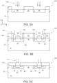
Figures 5A-5C are cross-sections similar toFigure 3 , in successive manufacturing steps of the present MOSFET device; and -
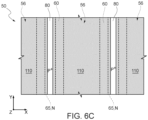
Figures 6A-6C are top views corresponding tofigures 5A-5C , in the manufacturing steps denoted by the same letter A-C. - The following description refers to the arrangement shown; consequently, expressions such as "above", "below", "top", "bottom", "right", "left" relate to the accompanying Figures and are not to be interpreted in a limiting manner.
-
Figures 3 and 4A show aMOSFET device 50 of a vertical conduction type, respectively in a cross-section taken in a plane XZ of a Cartesian reference system XYZ comprising a first axis X, a second axis Y and a third axis Z and in top view. - The
MOSFET device 50 is formed by a plurality of elementary cells which share a source terminal S and a drain terminal D. InFigures 3 and 4A , the elementary cells (shown only in part) are equal to each other and are arranged in parallel in a same die. - The
MOSFET device 50 is formed in asubstrate 55 of silicon carbide having afirst surface 55A and asecond surface 55B. - The
substrate 55 forms a drain region 57 (hereinafter also referred to as drift region), a plurality ofbody regions 60, a plurality of source regions 65 (here, twosource regions 65 for each body region 60) and a plurality of body contact regions 80 (onebody contact region 80 for each body region 60). - The
drain region 57, of a first conductivity type, here of N-type, extends between the first and thesecond surfaces substrate 55. - A
drain metallization region 59, of conductive material, for example of metal or silicide, extends over thesecond surface 55B of thesubstrate 55, in direct electrical contact with thedrain region 57, and forms the drain terminal D of theMOSFET device 50. - The
body regions 60 have a second conductivity type, here of P-type, and extend into thesubstrate 55 from thefirst surface 55A. Eachbody region 60 has a doping level for example comprised between 1.1017 atoms/cm3 and 1.1020 atoms/cm3, a depth (along the third axis Z) comprised between 0.3 um and 2 um and a width (along the first axis X) linked to the pitch (distance between adjacent cells), for example of 0.4-6 um. - In general, the
MOSFET device 50 has a plurality of body regions 60 (two shown inFigures 3 and 4A ), extending along the second axis Y and parallel to each other, as visible fromFigure 4A wherein, for clarity of illustration, the source metallization (see below) arranged above thefirst surface 55A of thesubstrate 55 is not shown. -
Adjacent body regions 60 delimit, therebetween,surface portions 56 of thedrain region 57, facing thefirst surface 55A of thesubstrate 55. - In a variant not shown, the
body regions 60 may have a circular or ring shape, in top view. - The
source regions 65 each extend from thefirst surface 55A of thesubstrate 55 inside arespective body region 60 and have the first conductivity type, here of N-type, for example with a doping level comprised between 1·1018 atoms/cm3 and 1·1020 atoms/cm3. - As indicated above, in the
MOSFET device 50, eachbody region 60 accommodates twosource regions 65 which are distinct and arranged side by side, at a mutual distance. - The
source regions 65, for example equal to each other, have the same depth, along the third axis Z, which is smaller than the depth of therespective body region 60. - Each
source region 65 and eachadjacent surface portion 56 of thedrain region 57 laterally delimit, inside arespective body region 60, achannel region 75. - In the
MOSFET device 50, in asame body region 60, abody contact region 80 extends between two adjacent source regions. - Each
body contact region 80 extends from thefirst surface 55A of thesubstrate 55, between tworespective source regions 65, in electrical contact with therespective body region 60, or slightly protruding into the latter, as represented inFigure 3 . - The
body contact regions 80, which have the aim of creating an ohmic contact for therespective body regions 60, are of the second conductivity type, here P-type, and have a higher doping level with respect to thebody regions 60. For example, thebody contact regions 80 have a doping level comprised between 1·1018 atoms/cm3 and 1·1020 atoms/cm3. Therefore, inFigure 3 , thebody contact regions 80 are of P+ type. - In practice, the width of the
body contact region 80, along the second direction X, is equal to the distance between thesource regions 65. - In addition, the
body contact regions 80 have a length, along the third axis Y, much greater than the width, along the second axis X. For example, thebody contact regions 80 have a length, along the third axis Y, greater than at least one hundred times, in general hundreds of times the width. - The
body contact regions 80 have a shape similar to that of thesource regions 65 and extend uninterruptedly therein throughout or approximately throughout their extension, as discussed below, with reference toFigure 4B . - In particular, in the
MOSFET device 50 ofFigures 3 and 4A , thebody contact regions 80 extend longitudinally (parallel to the second axis Y of the Cartesian reference system), inside thesource regions 65. - The
MOSFET device 50 also comprises a plurality of insulatedgate regions 70. Theinsulated gate regions 70 are each formed by agate insulating layer 71, in contact with thefirst surface 55A of thesubstrate 55; a gateconductive layer 72, directly superimposed on thegate insulating layer 71; and apassivation layer 73, covering the gateconductive layer 72 and sealing, together with thegate insulating layer 71, the gateconductive layer 72. - In detail, the
gate insulating layer 71 of aninsulated gate region 70 extends over arespective surface portion 56 of thedrain region 57, on twochannel regions 75 adjacent to therespective surface portion 56, and partially on twosource regions 65 adjacent to therespective channel regions 75. - The gate
conductive layers 72 of theinsulated gate regions 70 are electrically connected in parallel, in a manner not shown here, forming a gate terminal G of theMOSFET device 50. - The
MOSFET device 50 also comprises asource metallization region 83. - The
source metallization region 83, for example of metal and/or metal silicide, forms the source terminal S of theMOSFET device 50 and extends over thefirst surface 55A of thesubstrate 55, in direct electrical contact with thesource regions 65 and thebody contact regions 80. - As indicated above, the
body contact regions 80 may extend inside thesource regions 65 throughout their extension. This is shown inFigure 4B wherein, for clarity of illustration, thesource metallization 83 and theinsulated gate regions 70 are not shown and thebody contact regions 80 are even longer than thesource regions 65. - Fabrication of the
MOSFET device 50 comprises manufacturing steps similar to those of known devices, andonly the modification of the body contact and source masks,as discussed below in detail with reference toFigures 5A-5C and6A-6C . - In detail,
Figures 5a and6a show awafer 100 of silicon carbide, here having an N-type doping. - In
Figure 5A , thewafer 100 is processed to form thebody regions 60 inside thedrain region 57. In particular, using abody mask 101, for example of silicon oxide, which covers thesurface portions 56 of thedrain region 57, a masked implantation of P-type doping ions, such as aluminum or boron ions, is carried out, as schematically represented inFigure 5A byarrows 102. After the implant, an annealing may follow for activating the doping ions and reducing the defects in the crystalline lattice. - The implantation (with relative annealing) may occur in successive steps, also including successive epitaxial growths, using respective masks equal to each other, in a manner not shown.
- In
Figures 5B and6B , asource mask 104 is formed on thewafer 100, for example starting from thebody mask 101 ofFigure 5A . In this case, a masking layer, for example of oxide again, is deposited, lithographically defined to cover it at the center of thebody regions 60 and then etched anisotropically, so as to formsource mask 104 having, above thebody regions 60, side portions orspacers 105 on the sides of portions ofbody mask 101 andislands 106 at the center of thebody regions 60, extending therealong. Thesource mask 104 also covers thesurface portions 56 of thedrain region 7. - In particular, in the embodiment shown in
Figure 4B , theside portions 105 and theislands 106 extend throughout the length of thebody regions 60 in the direction of the second axis Y, so that the etch to form them affects them in a uniform manner. - Using the
source mask 104, N-type doping ions, such as nitrogen or phosphorus ions, are implanted inside thebody regions 60 and form the source regions 65 (arrows 107). - After the source implant, the
wafer 100 may be subject to an annealing step, in a known manner. -
Figures 5C and6C show the manufacturing step of thebody contact regions 80. - In detail, after removing the
source mask 104, abody contact mask 110 is formed, which covers thesurface portions 56 of thedrain region 57 and, above thebody regions 60, has a shape complementary with respect to thesource mask 104. - In particular, the
body contact mask 110 covers the newly implantedsource regions 65 and leaves uncovered only the portions of thebody regions 60 wherein it is desired to form thebody contact regions 80. - Then, using the
body contact mask 110, thebody contact regions 80 are implanted. The implant is performed at a high dose (for example comprised between 1014-5.1015), and suitable energy (for example comprised between 10 keV and 300 keV). - After a possible annealing step and the removal of the
body contact mask 110, thewafer 100 is processed in a known manner, forming theinsulated gate regions 70 on thewafer 100, thesource metallization region 83 and thedrain metallization region 59; then thewafer 100 is diced and provided with electrical connections to obtain thedevice 50 ofFigures 3, 4A and4B . - The
MOSFET device 50 and the manufacturing process thereof, here described, have numerous advantages. - In particular, by virtue of to the continuity of the
body contact regions 80, theMOSFET device 50 has a more uniform electric field distribution in the contact areas with thesource regions 65 andbody contact regions 80 with respect to similar known devices. - Furthermore, the charge carriers (recombinant holes) which move from the
channel regions 75 towards thebody contact regions 80 during turning off (diode operation) described above, find uniform paths and the paths for the charge carriers have substantially uniform resistivity along the extension of the body strips (along the second axis Y). - Furthermore, in the
MOSFET device 50 etch loading effects are no longer preset due to islands and discontinuities in thesource mask 104. - The
MOSFET device 50 has therefore improved electrical characteristics. - Finally, it is clear that modifications and variations may be made to the device and manufacturing process described and illustrated herein without thereby departing from the scope of the present invention, as defined in the attached claims.
- For example, in case the
body regions 6 and/or thesource regions 65 have a ring shape, in top view, thebody contact regions 80 may also have a continuous annular shape, without interruptions. - Instead of forming two
separate source regions 65, shielding the implant ofFigure 5B , the source implant might also be performed in the area of thebody contact region 80 and the implant of the latter (Figure 5C ) be carried out with a higher dose. - In summary, the MOSFET device of a vertical conduction type comprises:
- a substrate (55) of silicon carbide having a first conductivity type and a main face (55A);
- a body region (60) of a second conductivity type, extending into the substrate, from the main face, the body region having a first depth along a first direction (Z);
- a first and a second source region (65) of the first conductivity type, extending inside the body region (60), starting from the main face, parallel to each other, the source regions (65) having a second depth, along the first direction (Z), smaller than the first depth and being mutually spaced by a distance, in a second direction (X), perpendicular to the first direction (Z), the source regions (65) extending in an extension direction (Y), locally perpendicular to the first and the second directions (Z, X);
- a body contact region (80), of the second conductivity type, extending inside the body region (60), between the first and the second source regions (65), the body contact region (80) having a third depth, along the first direction, greater than or equal to the second depth (Z),
- wherein the body contact region (80) has a width, in the second direction (X) and a length, in the extension direction (Y), much greater than the width.
- The body region (60) has a length, in the extension direction (Y), at least one hundred times the width.
- The body contact region (80) extends continuously along the extension direction.
- The body contact region (80) may extend throughout the length of the source regions.
- The body contact region (80) may be a single body contact region (80).
- The width of the body contact region (80), in the second direction (X), may be equal to the distance between the source regions (65).
- The body contact region (80) may be contiguous to the source regions (65).
- The body region (60) may have a first doping level and the body contact region (80) may have a second doping level, higher than the first doping level.
- The extension direction may be a rectilinear longitudinal direction and the first, second and third directions may be Cartesian axes.
- The first conductivity type may be N and the second conductivity type may be P.
- A process for manufacturing a MOSFET device comprises:
- forming, in a substrate (55) of silicon carbide having a first conductivity type and a main face (55A), a body region (60) of a second conductivity type, the body region extending from the main face, having a first depth along a first direction (Z);
- forming, inside the body region (60), a first and a second source region (65) of the first conductivity type, extending from the main face and parallel to each other, the source regions (65) having a second depth, along the first direction, smaller than the first depth, being mutually spaced by a first distance, in a second direction (X), perpendicular to the first direction (Z), and extending in an extension direction (Y), locally perpendicular to the first and the second directions (Z, X);
- forming, inside the body region (60), between the first and the second source regions (65), a body contact region (80), of the second conductivity type, starting from the main face, the body contact region (80) having a third depth, along the first direction, greater than or equal to the second depth,
- wherein the body contact region (80) has a width, in the second direction (X) and a length, in the extension direction (Y), much greater than the width.
- Forming the first and the second source regions (65) may comprise introducing first doping ions, capable of conferring the first conductivity type, using a first mask (104), and wherein forming a body contact region (80) comprises introducing second doping ions, capable of conferring the second conductivity type, using a second mask (110) having masking portions extending to a second distance equal to the first distance and superimposed on the first and the second source regions (65).
- The second mask (110) may have a masking portion, above the body region (60), complementary to the first mask (104).
Claims (15)
- A MOSFET device (50) of a vertical conduction type comprising:a substrate (55) of silicon carbide having a first conductivity type and a main face (55A);a body region (60) of a second conductivity type, extending into the substrate (55) from the main face, the body region having a first depth along a first direction (Z) ;a first and a second source region (65) of the first conductivity type, extending inside the body region (60), from the main face, parallel to each other, the first and second source regions (65) having a second depth, along the first direction (Z), smaller than the first depth and being mutually spaced by a distance, in a second direction (X), perpendicular to the first direction (Z), the first and second source regions (65) extending in an extension direction (Y), locally perpendicular to the first and the second directions (Z, X);a body contact region (80), of the second conductivity type, extending inside the body region (60), between the first and the second source regions (65), the body contact region (80) having a third depth, along the first direction, greater than or equal to the second depth (Z),wherein the body contact region (80) has a width, in the second direction (X) and a length, in the extension direction (Y), greater than the width.
- The MOSFET device according to claim 1, wherein the length of body contact region (80) is at least one hundred times the width of the body contact region (80).
- The MOSFET device according to claim 1 or 2, wherein the body contact region (80) extends continuously along the extension direction.
- The MOSFET device according to any of the preceding claims, wherein the body contact region (80) extends throughout the length of the source regions (65).
- The MOSFET device according to any of the preceding claims, wherein the body contact region (80) is a single body contact region (80).
- The MOSFET device according to any of the preceding claims, wherein the width of the body contact region (80), in the second direction (X), is equal to the distance between the source regions (65).
- The MOSFET device according to any of the preceding claims, wherein the body contact region (80) is contiguous to the source regions (65).
- The MOSFET device according to any of the preceding claims, wherein the body region (60) has a first doping level and the body contact region (80) has a second doping level, higher than the first doping level.
- The MOSFET device according to any of the preceding claims, wherein the extension direction is a rectilinear longitudinal direction and the first, second and third directions are Cartesian axes.
- The MOSFET device according to any of the preceding claims, wherein the first conductivity type is N and the second conductivity type is P.
- A process for manufacturing a MOSFET device comprising:forming, in a substrate (55) of silicon carbide having a first conductivity type and a main face (55A), a body region (60) of a second conductivity type, the body region extending from the main face and having a first depth along a first direction (Z);forming, inside the body region (60), a first and a second source region (65) of the first conductivity type, extending from the main face and parallel to each other, the first and second source regions (65) having a second depth, along the first direction, smaller than the first depth, being mutually spaced by a first distance, in a second direction (X), perpendicular to the first direction (Z), and extending in an extension direction (Y), locally perpendicular to the first and the second directions (Z, X); andforming, inside the body region (60), between the first and the second source regions (65), a body contact region (80), of the second conductivity type, extending from the main face, the body contact region (80) having a third depth, along the first direction, greater than or equal to the second depth,wherein the body contact region (80) has a width, in the second direction (X) and a length, in the extension direction (Y), much greater than the width.
- The process according to the preceding claim, wherein forming the first and the second source regions (65) comprises introducing first doping ions, capable of conferring the first conductivity type, using a first mask (104), and wherein forming a body contact region (80) comprises introducing second doping ions, capable of conferring the second conductivity type, using a second mask (110) having masking portions extending to a second distance equal to the first distance and superimposed on the first and the second source regions (65).
- The process according to the preceding claim, wherein the second mask (110) has a masking portion, above the body region (60), complementary to the first mask (104).
- The process according to claim 12 or 13, comprising:forming a body mask (101) and performing a first ion implantation process in a presence of the body mask to form the body region (60);performing a first thermal annealing process;performing a second ion implantation process in presence of the first mask (104) to form the first and second source regions;performing a second thermal annealing process;performing a third ion implantation process in presence of the second mask (110) to form the body contact region andperforming a third thermal annealing process.
- The process according to the preceding claim, comprising forming the first mask (104) at least partially on top of the body mask (101).
Applications Claiming Priority (1)
| Application Number | Priority Date | Filing Date | Title |
|---|---|---|---|
| IT102023000001482A IT202300001482A1 (en) | 2023-01-31 | 2023-01-31 | SILICON CARBIDE POWER MOSFET DEVICE WITH IMPROVED PERFORMANCE AND RELATED MANUFACTURING PROCESS |
Publications (1)
| Publication Number | Publication Date |
|---|---|
| EP4411830A1 true EP4411830A1 (en) | 2024-08-07 |
Family
ID=85792050
Family Applications (1)
| Application Number | Title | Priority Date | Filing Date |
|---|---|---|---|
| EP24153621.8A Pending EP4411830A1 (en) | 2023-01-31 | 2024-01-24 | Silicon carbide power mosfet device having improved performances and manufacturing process thereof |
Country Status (5)
| Country | Link |
|---|---|
| US (1) | US20240258377A1 (en) |
| EP (1) | EP4411830A1 (en) |
| JP (1) | JP2024109061A (en) |
| CN (1) | CN118431285A (en) |
| IT (1) | IT202300001482A1 (en) |
Families Citing this family (1)
| Publication number | Priority date | Publication date | Assignee | Title |
|---|---|---|---|---|
| US12349444B1 (en) * | 2024-04-11 | 2025-07-01 | Globalfoundries Singapore Pte. Ltd | Under-source body contact |
Citations (4)
| Publication number | Priority date | Publication date | Assignee | Title |
|---|---|---|---|---|
| US20100048004A1 (en) * | 2007-01-16 | 2010-02-25 | Koichi Hashimoto | Semiconductor device and process for manufacturing the same |
| US8476697B1 (en) * | 2003-04-11 | 2013-07-02 | Purdue Research Foundation | Short-channel silicon carbide power MOSFET |
| US20150270354A1 (en) * | 2014-03-20 | 2015-09-24 | Kabushiki Kaisha Toshiba | Semiconductor device and method for producing the same |
| WO2016084141A1 (en) * | 2014-11-26 | 2016-06-02 | 株式会社日立製作所 | Semiconductor switching element and silicon carbide semiconductor device manufacturing method |
Family Cites Families (4)
| Publication number | Priority date | Publication date | Assignee | Title |
|---|---|---|---|---|
| JP3617507B2 (en) * | 2002-07-01 | 2005-02-09 | 日産自動車株式会社 | Silicon carbide semiconductor device manufacturing method and silicon carbide semiconductor device manufactured by the manufacturing method |
| JP2015099845A (en) * | 2013-11-19 | 2015-05-28 | 住友電気工業株式会社 | Semiconductor device |
| US11018228B2 (en) * | 2019-08-07 | 2021-05-25 | Fast SiC Semiconductor Incorporated | Silicon carbide semiconductor device |
| JP7547262B2 (en) * | 2021-03-18 | 2024-09-09 | 株式会社東芝 | Semiconductor device, semiconductor device manufacturing method, inverter circuit, drive device, vehicle, and elevator |
-
2023
- 2023-01-31 IT IT102023000001482A patent/IT202300001482A1/en unknown
-
2024
- 2024-01-09 US US18/408,474 patent/US20240258377A1/en active Pending
- 2024-01-17 JP JP2024005486A patent/JP2024109061A/en active Pending
- 2024-01-24 EP EP24153621.8A patent/EP4411830A1/en active Pending
- 2024-01-29 CN CN202410120236.2A patent/CN118431285A/en active Pending
Patent Citations (4)
| Publication number | Priority date | Publication date | Assignee | Title |
|---|---|---|---|---|
| US8476697B1 (en) * | 2003-04-11 | 2013-07-02 | Purdue Research Foundation | Short-channel silicon carbide power MOSFET |
| US20100048004A1 (en) * | 2007-01-16 | 2010-02-25 | Koichi Hashimoto | Semiconductor device and process for manufacturing the same |
| US20150270354A1 (en) * | 2014-03-20 | 2015-09-24 | Kabushiki Kaisha Toshiba | Semiconductor device and method for producing the same |
| WO2016084141A1 (en) * | 2014-11-26 | 2016-06-02 | 株式会社日立製作所 | Semiconductor switching element and silicon carbide semiconductor device manufacturing method |
Also Published As
| Publication number | Publication date |
|---|---|
| IT202300001482A1 (en) | 2024-07-31 |
| US20240258377A1 (en) | 2024-08-01 |
| JP2024109061A (en) | 2024-08-13 |
| CN118431285A (en) | 2024-08-02 |
Similar Documents
| Publication | Publication Date | Title |
|---|---|---|
| JP7182594B2 (en) | Power semiconductor device with gate trench and buried termination structure and related method | |
| JP7724284B2 (en) | Trench-type power devices with improved reliability and continuity | |
| US12376319B2 (en) | Support shield structures for trenched semiconductor devices | |
| EP4244898A1 (en) | Semiconductor power devices having multiple gate trenches and methods of forming such devices | |
| US11164967B2 (en) | Power silicon carbide based MOSFET transistors with improved short circuit capabilities and methods of making such devices | |
| GB2309589A (en) | Forming doped layers of semiconductor devices | |
| CN112635562B (en) | Semiconductor device including current spreading region | |
| US12205983B2 (en) | Semiconductor device and manufacturing method of semiconductor device | |
| CN117096190A (en) | Power switching device with high DV/DT capability and method of making such device | |
| JP2023529342A (en) | Semiconductor power device with graded lateral doping and method of forming such device | |
| US20240258377A1 (en) | Silicon carbide power mosfet device having improved performances and manufacturing process thereof | |
| CN114823846A (en) | Guard ring for coupling of edge termination | |
| CN113424327B (en) | Systems and methods for unipolar charge-balanced semiconductor power devices | |
| JP7824082B2 (en) | Silicon carbide vertical conduction MOSFET device and method for fabricating same | |
| KR102406116B1 (en) | Semiconductor device and method manufacturing the same | |
| CN114823906A (en) | Silicon carbide vertical conduction MOSFET device and manufacturing process thereof | |
| US20250113531A1 (en) | Power silicon carbide based semiconductor devices with selective jfet implants that are self-aligned with the well regions and methods of making such devices | |
| US20250311318A1 (en) | Power silicon carbide based semiconductor devices having super junction drift regions and methods of forming such devices | |
| US20250159948A1 (en) | Split support shield structures for trenched semiconductor devices with integrated schottky diodes | |
| JP2023549543A (en) | Vertical semiconductor device and its manufacturing method | |
| KR101870824B1 (en) | Power semiconductor device and method of fabricating the same | |
| JP2024125203A (en) | Process for manufacturing a power electronic device having a current spreading layer - Patents.com | |
| CN119300385A (en) | Method of manufacturing semiconductor device including ion implantation process | |
| CN116825846A (en) | A high-reliability semiconductor device and its manufacturing method | |
| KR20150108485A (en) | Method for reducing on resistance of Power MOSFET JFET area by double implanting ion |
Legal Events
| Date | Code | Title | Description |
|---|---|---|---|
| PUAI | Public reference made under article 153(3) epc to a published international application that has entered the european phase |
Free format text: ORIGINAL CODE: 0009012 |
|
| STAA | Information on the status of an ep patent application or granted ep patent |
Free format text: STATUS: THE APPLICATION HAS BEEN PUBLISHED |
|
| AK | Designated contracting states |
Kind code of ref document: A1 Designated state(s): AL AT BE BG CH CY CZ DE DK EE ES FI FR GB GR HR HU IE IS IT LI LT LU LV MC ME MK MT NL NO PL PT RO RS SE SI SK SM TR |
|
| STAA | Information on the status of an ep patent application or granted ep patent |
Free format text: STATUS: REQUEST FOR EXAMINATION WAS MADE |
|
| 17P | Request for examination filed |
Effective date: 20250206 |