EP4411826A1 - Bidirectional thyristor - Google Patents
Bidirectional thyristor Download PDFInfo
- Publication number
- EP4411826A1 EP4411826A1 EP22829639.8A EP22829639A EP4411826A1 EP 4411826 A1 EP4411826 A1 EP 4411826A1 EP 22829639 A EP22829639 A EP 22829639A EP 4411826 A1 EP4411826 A1 EP 4411826A1
- Authority
- EP
- European Patent Office
- Prior art keywords
- conductivity
- type semiconductor
- semiconductor layer
- electrode
- emitting portions
- Prior art date
- Legal status (The legal status is an assumption and is not a legal conclusion. Google has not performed a legal analysis and makes no representation as to the accuracy of the status listed.)
- Pending
Links
Images





Classifications
-
- H—ELECTRICITY
- H10—SEMICONDUCTOR DEVICES; ELECTRIC SOLID-STATE DEVICES NOT OTHERWISE PROVIDED FOR
- H10D—INORGANIC ELECTRIC SEMICONDUCTOR DEVICES
- H10D18/00—Thyristors
-
- H—ELECTRICITY
- H10—SEMICONDUCTOR DEVICES; ELECTRIC SOLID-STATE DEVICES NOT OTHERWISE PROVIDED FOR
- H10D—INORGANIC ELECTRIC SEMICONDUCTOR DEVICES
- H10D18/00—Thyristors
- H10D18/80—Bidirectional devices, e.g. triacs
-
- H—ELECTRICITY
- H10—SEMICONDUCTOR DEVICES; ELECTRIC SOLID-STATE DEVICES NOT OTHERWISE PROVIDED FOR
- H10D—INORGANIC ELECTRIC SEMICONDUCTOR DEVICES
- H10D62/00—Semiconductor bodies, or regions thereof, of devices having potential barriers
- H10D62/10—Shapes, relative sizes or dispositions of the regions of the semiconductor bodies; Shapes of the semiconductor bodies
- H10D62/124—Shapes, relative sizes or dispositions of the regions of semiconductor bodies or of junctions between the regions
- H10D62/126—Top-view geometrical layouts of the regions or the junctions
-
- H—ELECTRICITY
- H10—SEMICONDUCTOR DEVICES; ELECTRIC SOLID-STATE DEVICES NOT OTHERWISE PROVIDED FOR
- H10D—INORGANIC ELECTRIC SEMICONDUCTOR DEVICES
- H10D62/00—Semiconductor bodies, or regions thereof, of devices having potential barriers
- H10D62/10—Shapes, relative sizes or dispositions of the regions of the semiconductor bodies; Shapes of the semiconductor bodies
- H10D62/13—Semiconductor regions connected to electrodes carrying current to be rectified, amplified or switched, e.g. source or drain regions
- H10D62/133—Emitter regions of BJTs
-
- H—ELECTRICITY
- H10—SEMICONDUCTOR DEVICES; ELECTRIC SOLID-STATE DEVICES NOT OTHERWISE PROVIDED FOR
- H10D—INORGANIC ELECTRIC SEMICONDUCTOR DEVICES
- H10D62/00—Semiconductor bodies, or regions thereof, of devices having potential barriers
- H10D62/10—Shapes, relative sizes or dispositions of the regions of the semiconductor bodies; Shapes of the semiconductor bodies
- H10D62/13—Semiconductor regions connected to electrodes carrying current to be rectified, amplified or switched, e.g. source or drain regions
- H10D62/141—Anode or cathode regions of thyristors; Collector or emitter regions of gated bipolar-mode devices, e.g. of IGBTs
- H10D62/148—Cathode regions of thyristors
Definitions
- the present invention relates to a bidirectional thyristor.
- Various aspects of the present invention have an object to provide a bidirectional thyristor capable of improving (dv/dt)c capability.
- two or more of the plurality of carrier emitting portions are disposed in contact with the outer edge of the first electrode. Even when a part of the plurality of carrier emitting portions are disposed at the outer edge of the first electrode, the reduction in area of the third second-conductivity-type impurity diffusion layer in contact with the first electrode is significantly small, which hardly affects VT characteristics and gate characteristics.
- ground When ground (GND) is connected to the first electrode, a negative voltage is applied to the second electrode, and a negative voltage is applied to the gate electrode, a gate trigger current flows, so that a current flows through the first electrode, the first first-conductivity-type semiconductor layer, the first second-conductivity-type semiconductor layer, the second first-conductivity-type semiconductor layer, the second second-conductivity-type semiconductor layer, and the second electrode in this order due to thyristor operation.
- carriers 23 are diffused in a transverse direction, and the carriers remain even after the current stops flowing due to the thyristor operation.
- the density of carrier emitting portions in a vicinity of the outer edge of the first electrode is higher than the density of carrier emitting portions in a region other than the vicinity of the outer edge of the first electrode.
- the remaining carriers can be more effectively processed as ineffective current not via the third second-conductivity-type semiconductor layer but through the carrier emitting portions disposed in the vicinity of the outer edge of the first electrode.
- a bidirectional thyristor in item [1] includes:
- FIG. 1 is a plan view illustrating a bidirectional thyristor according to one aspect of the present invention.
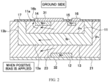
- FIG. 2 is a cross-sectional view taken along the line A-A' illustrated in FIG. 1 . Note that the cross-sectional view of the bidirectional thyristor illustrated in FIG. 2 omits a part of the bidirectional thyristor illustrated in FIG. 1 .
- a first first-conductivity-type semiconductor layer (P + ) 11 is formed on a front surface side (T1 electrode 31 side) of a second first-conductivity-type semiconductor layer (P + ) 21 as a P+ type semiconductor substrate illustrated in FIG. 2 .
- a first second-conductivity-type semiconductor layer (N - ) 13 is disposed (see FIG. 2 ).
- the first second-conductivity-type semiconductor layer (N - ) 13 is formed such that the outer periphery (both ends illustrated in FIG. 2 ) thereof extends to the front surface side of the first first-conductivity-type semiconductor layer (P + ) 11 (see FIG. 1 and FIG. 2 ).
- the first second-conductivity-type semiconductor layer (N - ) 13 is formed such that the first first-conductivity-type semiconductor layer (P + ) 11 is surrounded by a bottom portion 13a and side wall portions 13b.
- a second first-conductivity-type semiconductor layer (P + ) 21 is disposed on a rear surface side (T2 electrode 32 side) of the first second-conductivity-type semiconductor layer (N - ) 13.
- a second second-conductivity-type semiconductor layer (N + ) 12 is formed, and the second second-conductivity-type semiconductor layer (N + ) 12 is located on the rear surface side (T2 electrode 32 side) of the second first-conductivity-type semiconductor layer (P + ) 21.
- the second second-conductivity-type semiconductor layer (N + ) 12 is located on the rear surface side (T2 electrode 32 side) of the second first-conductivity-type semiconductor layer (P + ) 21.
- the first first-conductivity-type semiconductor layer (P + ) 11, the first second-conductivity-type semiconductor layer (N - ) 13, the second first-conductivity-type semiconductor layer (P + ) 21, and the second second-conductivity-type semiconductor layer (N + ) 12 are disposed in this order in a direction (first direction) from the front surface to the rear surface of the first first-conductivity-type semiconductor layer (P + ) 11, and these layers serve as a first path through which a current flows due to thyristor operation.
- a third second-conductivity-type semiconductor layer (N + ) 14 is disposed on the front surface side (T1 electrode 31 side) of the first first-conductivity-type semiconductor layer (P + ) 11, a third second-conductivity-type semiconductor layer (N + ) 14 is disposed.
- the second first-conductivity-type semiconductor layer (P + ) 21, the first second-conductivity-type semiconductor layer (N - ) 13, the first first-conductivity-type semiconductor layer (P + ) 11, and the third second-conductivity-type semiconductor layer (N + ) 14 are disposed in this order in a direction (second direction) from the rear surface to the front surface of the second first-conductivity-type semiconductor layer (P + ) 21, and these layers serve as a second path through which a current flows due to thyristor operation.
- a plurality of carrier emitting portions 11a are disposed on the third second-conductivity-type semiconductor layer (N + ) 14.
- a fourth second-conductivity-type semiconductor layer (N + ) 15 is disposed on the front surface side of the first first-conductivity-type semiconductor layer (P + ) 11.
- a first electrode (T1 electrode) 31 is disposed in contact with the third second-conductivity-type semiconductor layer (N + ) 14, the plurality of carrier emitting portions 11a, and the first first-conductivity-type semiconductor layer (P + ) 11.
- a second electrode (T2 electrode) 32 is disposed in contact with the second second-conductivity-type semiconductor layer (N + ) 12 and the second first-conductivity-type semiconductor layer (P + ) 21.
- a gate electrode 16 is disposed in contact with the fourth second-conductivity-type semiconductor layer (N + ) 15 and the first first-conductivity-type semiconductor layer (P + ) 11.
- a passivation film 17 is disposed on a boundary between the first first-conductivity-type semiconductor layer (P + ) 11 and the first second-conductivity-type semiconductor layer (N - ) 13 and a boundary between the first second-conductivity-type semiconductor layer (N - ) 13 and the second first-conductivity-type semiconductor layer (P + ) 21 on the front surface side of the first first-conductivity-type semiconductor layer (P + ) 11.
- the passivation film 17 only needs to be disposed on at least the boundaries, but a passivation film may be disposed on a portion other than the boundaries (see FIG. 2 ).
- Each of the plurality of carrier emitting portions 11a illustrated in FIG. 1 is configured such that an opening is formed in the third second-conductivity-type semiconductor layer (N + ) 14 and the first first-conductivity-type semiconductor layer (P + ) 11 is located in the opening. In this manner, the plurality of carrier emitting portions 11a are disposed in contact with the first electrode (T1 electrode) illustrated in FIG. 2 .
- the plurality of carrier emitting portions 11a are disposed between a position 16a apart from the gate electrode 16 by a predetermined distance and an outer edge 16b of the first electrode (T1 electrode) 31 that is an inner edge of the passivation film 17.
- FIG. 3 and FIG. 4 correspond to FIG. 2 , and are cross-sectional views for describing functions and effects of the bidirectional thyristor according to one aspect of the present invention.
- the same parts as in FIG. 2 are denoted by the same reference symbols.
- FIG. 5 is a cross-sectional view illustrating a comparative example in which the carrier emitting portions 11a have been removed from the bidirectional thyristor according to one aspect of the present invention illustrated in FIG. 2 , and is a cross-sectional view for describing a fact that when there is no carrier emitting portion 11a, false turn-on 42 is more likely to occur.
- the same parts as in FIG. 2 are denoted by the same reference symbols.
- Two or more of the plurality of carrier emitting portions 11a are disposed in contact with the outer edge 16b of the first electrode (T1 electrode) 31.
- the reduction in area of the third second-conductivity-type impurity diffusion layer (N + ) 14 in contact with the first electrode (T1 electrode) 31 is significantly small, which hardly affects VT characteristics and gate characteristics.
- the outer edge 16b of the first electrode (T1 electrode) 31 in contact with two or more of the plurality of carrier emitting portions 11a contacts the passivation film 17 (see FIG. 2 ).
- remaining carriers 23 that remain under the passivation film 17 can also be more effectively processed as ineffective current not via the third second-conductivity-type semiconductor layer (N + ) 14 but through the carrier emitting portions 11a disposed at the outer edge 16b of the first electrode (T1 electrode) 31.
- false turn-on can be more effectively prevented.
- a current i when false turn-on occurs can be expressed by the following expression. As dv/dt of the positive bias becomes steeper, a current caused by the remaining carriers 23 becomes larger, and false turn-on is more likely to occur.
- FIG. 6 illustrates a bidirectional thyristor having this structure.
- FIG. 6 is a view corresponding to FIG. 2 , and is a comparative example of the present invention. The same parts as in FIG. 2 are denoted by the same reference symbols.
- a distance ⁇ of vertical N + that is, distance ⁇ between third second-conductivity-type semiconductor layer (N + ) 14 and second second-conductivity-type semiconductor layer (N + ) 12 in planar direction
- a movement distance of carriers 23 in the transverse direction can be secured. Accordingly, the remaining carriers 23 are less likely to reach an adjacent thyristor. As a result, false turn-on can be prevented.
- the bidirectional thyristor in the comparative example illustrated in FIG. 6 has the same chip size as the bidirectional thyristor illustrated in FIG. 2 , the area of the third second-conductivity-type semiconductor layer (N + ) 14 or the second second-conductivity-type semiconductor layer (N + ) 12 in the bidirectional thyristor in the comparative example illustrated in FIG. 6 is reduced due to the above-mentioned distance ⁇ as compared to the bidirectional thyristor illustrated in FIG. 2 .
- VT increases or gate characteristics are affected occurs.
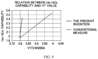
- FIG. 9 is a diagram illustrating a result of preparing a sample of the bidirectional thyristor of the present invention illustrated in FIG. 2 and a sample in the comparative example illustrated in FIG. 5 and measuring the relations between VT (turn-on voltage) and (dv/dt)c capability.
- FIG. 10 is a diagram illustrating a result of preparing a sample of the bidirectional thyristor of the present invention illustrated in FIG. 2 and a sample in the comparative example illustrated in FIG. 5 and measuring the relations between IGT (gate trigger current) and (dv/dt)c capability.
- FIG. 11 is a diagram illustrating a result of preparing a sample of the bidirectional thyristor of the present invention illustrated in FIG. 2 and a sample in the comparative example illustrated in FIG. 5 and measuring the relations between VGT (gate trigger voltage) and (dv/dt)c capability.
- TEE PRESENT INVENTION corresponds to the measurement results of the sample of the bidirectional thyristor of the present invention illustrated in FIG. 2
- CONVENTIONAL MEASURES corresponds to the measurement results of the sample in the comparative example illustrated in FIG. 5 .
- two or more carrier emitting portions 11a disposed in contact with the outer edge 16b of the first electrode (T1 electrode) 31 may have a cutout shape, a polygonal shape, or an elliptical shape in plan view.
- FIG. 7 is a plan view illustrating Modification 1 of the bidirectional thyristor illustrated in FIG. 1 .
- FIG. 8 is a plan view illustrating Modification 2 of the bidirectional thyristor illustrated in FIG. 1 . Note that, in FIG. 7 and FIG. 8 , the same parts as in FIG. 1 are denoted by the same reference symbols.
- two or more carrier emitting portions 11a disposed in contact with the outer edge of the first electrode (T1) may have a cutout shape, a polygonal shape, or an elliptical shape in plan view.
- the density of carrier emitting portions 11a in the vicinity of the outer edge 16b of the first electrode (T1 electrode) 31 be higher than the density of carrier emitting portions 11a in a region other than the vicinity of the outer edge 16b of the first electrode (T1 electrode) 31.
- the density of the carrier emitting portions 11a in the vicinity of the outer edge 16b of the first electrode (T1) may be higher than the density of the carrier emitting portion 11a in a region other than the vicinity of the outer edge 16b of the first electrode (T1).
- the density as used herein refers to a value obtained by dividing the number of carrier emitting portions 11a in the vicinity of the outer edge 16b of the first electrode (T1) illustrated in FIG. 1 by the area of a planar region of the vicinity of the outer edge 16b of the first electrode (T1). As a result, the remaining carriers 11a illustrated in FIG.
- the carrier emitting portions 11a in the vicinity of the outer edge 16b of the first electrode (T1) refer to carrier emitting portions 11a that form a triangle 33 illustrated in FIG. 1 .
- the triangle 33 is a triangle 33 formed by adjacent carrier emitting portions 11a located at the outer edge 16b of the first electrode (T1) and a carrier emitting portion 11a located at the shortest distance from a straight line that connects the adjacent carrier emitting portions 11a.
Landscapes
- Thyristors (AREA)
Abstract
Description
- This patent application claims the benefit and priority of
Japanese Patent Application No. 2021-158660 filed on September 29, 2021 - The present invention relates to a bidirectional thyristor.
- In conventional bidirectional thyristors, even immediately after a current flows from a first electrode (T1 electrode) to a second electrode (T2 electrode) to perform thyristor operation and the current stops flowing, carriers remain and are diffused in a transverse direction. Thus, when bias is applied to the second electrode (T2 electrode), even if bias is not applied to a gate electrode, the remaining carriers exhibit the same effect as a gate trigger current, and a phenomenon of false turn-on, which shifts to on-operation, may occur. The less possibility of false turn-on is expressed by (dv/dt)c capability, and the improvement in (dv/dt)c capability is sought after while securing thyristor characteristics. Note that a conventional bidirectional thyristor is disclosed in, for example,
Japanese Patent Application Publication No. 2010-245377 - Various aspects of the present invention have an object to provide a bidirectional thyristor capable of improving (dv/dt)c capability.
- Various aspects of the present invention are described below.
- [1] A bidirectional thyristor, including:
- a first first-conductivity-type semiconductor layer;
- a first second-conductivity-type semiconductor layer disposed on a rear surface side of the first first-conductivity-type semiconductor layer;
- a second first-conductivity-type semiconductor layer disposed on a rear surface side of the first second-conductivity-type semiconductor layer;
- a second second-conductivity-type semiconductor layer disposed on a rear surface side of the second first-conductivity-type semiconductor layer;
- a third second-conductivity-type semiconductor layer disposed on a front surface side of the first first-conductivity-type semiconductor layer;
- a plurality of carrier emitting portions disposed on the third second-conductivity-type semiconductor layers;
- a fourth second-conductivity-type semiconductor layer disposed on the front surface side of the first first-conductivity-type semiconductor layer;
- a first electrode that contacts the third second-conductivity-type semiconductor layer, the plurality of carrier emitting portions, and the first first-conductivity-type semiconductor layer;
- a second electrode that contacts the second second-conductivity-type semiconductor layer and the second first-conductivity-type semiconductor layer;
- a gate electrode that contacts the fourth second-conductivity-type semiconductor layer and the first first-conductivity-type semiconductor layer; and
- a passivation film disposed on a boundary between the first first-conductivity-type semiconductor layer and the first second-conductivity-type semiconductor layer and a boundary between the first second-conductivity-type semiconductor layer and the second first-conductivity-type semiconductor layer on the front surface side of the first first-conductivity-type semiconductor layer, in which
- each of the plurality of carrier emitting portions is configured such that an opening is formed in the third second-conductivity-type semiconductor layer and the first first-conductivity-type semiconductor layer is located in the opening,
- in plan view, the plurality of carrier emitting portions are disposed between a position away from the gate electrode by a predetermined distance and an outer edge of the first electrode,
- two or more of the plurality of carrier emitting portions are disposed in contact with the outer edge of the first electrode,
- the outer edge of the first electrode in contact with two or more of the plurality of carrier emitting portions contacts the passivation film, and
- in plan view, an area of a triangle formed by adjacent carrier emitting portions located at the outer edge of the first electrode and a carrier emitting portion located at a shortest distance from a straight line connecting the adjacent carrier emitting portions is smaller than an area of a quadrangle formed by carrier emitting portions that are not located at the outer edge of the first electrode.
- [2] The bidirectional thyristor according to item [1], in which the two or more carrier emitting portions disposed in contact with the outer edge of the first electrode have a cutout shape, a polygonal shape, or an elliptical shape in plan view.
- [3] The bidirectional thyristor according to item [1] or [2], in which, in plan view, a density of carrier emitting portions in a vicinity of the outer edge of the first electrode is higher than a density of carrier emitting portions in a region other than the vicinity of the outer edge of the first electrode.
- In the bidirectional thyristor according to item [1] of the present invention, two or more of the plurality of carrier emitting portions are disposed in contact with the outer edge of the first electrode. Even when a part of the plurality of carrier emitting portions are disposed at the outer edge of the first electrode, the reduction in area of the third second-conductivity-type impurity diffusion layer in contact with the first electrode is significantly small, which hardly affects VT characteristics and gate characteristics.
- When ground (GND) is connected to the first electrode, a negative voltage is applied to the second electrode, and a negative voltage is applied to the gate electrode, a gate trigger current flows, so that a current flows through the first electrode, the first first-conductivity-type semiconductor layer, the first second-conductivity-type semiconductor layer, the second first-conductivity-type semiconductor layer, the second second-conductivity-type semiconductor layer, and the second electrode in this order due to thyristor operation. In this case,
carriers 23 are diffused in a transverse direction, and the carriers remain even after the current stops flowing due to the thyristor operation. Next, when no bias is applied to the gate electrode and a positive voltage is applied to the second electrode, the remaining carriers are processed as ineffective current not via the third second-conductivity-type semiconductor layer but through the plurality of carrier emitting portions, thereby preventing false turn-on. In this case, in plan view, by setting the area of a triangle formed by adjacent carrier emitting portions located at the outer edge of the first electrode and a carrier emitting portion located at the shortest distance from a straight line connecting the adjacent carrier emitting portion to be smaller than the area of aquadrangle 22 formed by carrier emitting portions that are not located at the outer edge of the first electrode, remaining carriers can be more effectively processed as ineffective current. Thus, false turn-on can be more effectively prevented, and (dv/dt)c capability can be improved. - In the bidirectional thyristor according to item [3] of the present invention, in plan view, the density of carrier emitting portions in a vicinity of the outer edge of the first electrode is higher than the density of carrier emitting portions in a region other than the vicinity of the outer edge of the first electrode. As a result, the remaining carriers can be more effectively processed as ineffective current not via the third second-conductivity-type semiconductor layer but through the carrier emitting portions disposed in the vicinity of the outer edge of the first electrode.
-
-
FIG. 1 is a plan view illustrating a bidirectional thyristor according to one aspect of the present invention; -
FIG. 2 is a cross-sectional view taken along the line A-A' illustrated inFIG. 1 ; -
FIG. 3 is a cross-sectional view corresponding toFIG. 2 , for describing functions and effects of the bidirectional thyristor according to one aspect of the present invention; -
FIG. 4 is a cross-sectional view corresponding toFIG. 2 , for describing functions and effects of the bidirectional thyristor according to one aspect of the present invention; -
FIG. 5 is a cross-sectional view illustrating a comparative example in whichcarrier emitting portions 11a have been removed from the bidirectional thyristor according to one aspect of the present invention illustrated inFIG. 2 ; -
FIG. 6 is a view corresponding toFIG. 2 , and is a comparative example of the present invention; -
FIG. 7 is a plan view illustrating Modification 1 of the bidirectional thyristor illustrated inFIG. 1 ; -
FIG. 8 is a planview illustrating Modification 2 of the bidirectional thyristor illustrated inFIG. 1 ; -
FIG. 9 is a diagram illustrating a result of preparing a sample of the bidirectional thyristor of the present invention illustrated inFIG. 2 and a sample in the comparative example illustrated inFIG. 5 and measuring the relations between VT (turn-on voltage) and (dv/dt)c capability; -
FIG. 10 is a diagram illustrating a result of preparing the sample of the bidirectional thyristor of the present invention illustrated inFIG. 2 and the sample in the comparative example illustrated inFIG. 5 and measuring the relations between IGT (gate trigger current) and (dv/dt)c capability; and -
FIG. 11 is a diagram illustrating a result of preparing the sample of the bidirectional thyristor of the present invention illustrated inFIG. 2 and the sample in the comparative example illustrated inFIG. 5 and measuring the relations between VGT (gate trigger voltage) and (dv/dt)c capability. - Embodiments of the present invention are described in detail below with reference to the drawings. The present invention is not limited to the following description, and a person skilled in the art could easily understand that the forms and details of the present invention can be variously changed without departing from the gist and scope of the present invention. Thus, the present invention is not intended to be interpreted as being limited to the following description of the embodiments.
- A bidirectional thyristor in item [1] according to one aspect of the present invention includes:
- a first first-conductivity-type semiconductor layer;
- a first second-conductivity-type semiconductor layer disposed on a rear surface side of the first first-conductivity-type semiconductor layer;
- a second first-conductivity-type semiconductor layer disposed on a rear surface side of the first second-conductivity-type semiconductor layer;
- a second second-conductivity-type semiconductor layer disposed on a rear surface side of the second first-conductivity-type semiconductor layer;
- a third second-conductivity-type semiconductor layer disposed on a front surface side of the first first-conductivity-type semiconductor layer;
- a plurality of carrier emitting portions disposed on the third second-conductivity-type semiconductor layer;
- a fourth second-conductivity-type semiconductor layer disposed on the front surface side of the first first-conductivity-type semiconductor layer;
- a first electrode that contacts the third second-conductivity-type semiconductor layer, the plurality of carrier emitting portions, and the first first-conductivity-type semiconductor layer;
- a second electrode that contacts the second second-conductivity-type semiconductor layer and the second first-conductivity-type semiconductor layer;
- a gate electrode that contacts the fourth second-conductivity-type semiconductor layer and the first first-conductivity-type semiconductor layer; and
- a passivation film disposed on a boundary between the first first-conductivity-type semiconductor layer and the first second-conductivity-type semiconductor layer and a boundary between the first second-conductivity-type semiconductor layer and the second first-conductivity-type semiconductor layer on the front surface side of the first first-conductivity-type semiconductor layer, in which
- each of the plurality of carrier emitting portions is configured such that an opening is formed in the third second-conductivity-type semiconductor layer and the first first-conductivity-type semiconductor layer is located in the opening,
- in plan view, the plurality of carrier emitting portions are disposed between a position away from the gate electrode by a predetermined distance and an outer edge of the first electrode,
- two or more of the plurality of carrier emitting portions are disposed in contact with the outer edge of the first electrode,
- the outer edge of the first electrode in contact with two or more of the plurality of carrier emitting portions contacts the passivation film, and
- in plan view, an area of a triangle formed by adjacent carrier emitting portions located at the outer edge of the first electrode and a carrier emitting portion located at a shortest distance from a straight line connecting the adjacent carrier emitting portions is smaller than an area of a quadrangle formed by carrier emitting portions that are not located at the outer edge of the first electrode.
-
FIG. 1 is a plan view illustrating a bidirectional thyristor according to one aspect of the present invention.FIG. 2 is a cross-sectional view taken along the line A-A' illustrated inFIG. 1 . Note that the cross-sectional view of the bidirectional thyristor illustrated inFIG. 2 omits a part of the bidirectional thyristor illustrated inFIG. 1 . - A first first-conductivity-type semiconductor layer (P+) 11 is formed on a front surface side (
T1 electrode 31 side) of a second first-conductivity-type semiconductor layer (P+) 21 as a P+ type semiconductor substrate illustrated inFIG. 2 . - On a rear surface side (
T2 electrode 32 side) of the first first-conductivity-type semiconductor layer (P+) 11, a first second-conductivity-type semiconductor layer (N-) 13 is disposed (seeFIG. 2 ). - The first second-conductivity-type semiconductor layer (N-) 13 is formed such that the outer periphery (both ends illustrated in
FIG. 2 ) thereof extends to the front surface side of the first first-conductivity-type semiconductor layer (P+) 11 (seeFIG. 1 andFIG. 2 ). In other words, as illustrated inFIG. 2 , the first second-conductivity-type semiconductor layer (N-) 13 is formed such that the first first-conductivity-type semiconductor layer (P+) 11 is surrounded by abottom portion 13a andside wall portions 13b. - On a rear surface side (
T2 electrode 32 side) of the first second-conductivity-type semiconductor layer (N-) 13, a second first-conductivity-type semiconductor layer (P+) 21 is disposed. - On the second first-conductivity-type semiconductor layer (P+) 21, a second second-conductivity-type semiconductor layer (N+) 12 is formed, and the second second-conductivity-type semiconductor layer (N+) 12 is located on the rear surface side (
T2 electrode 32 side) of the second first-conductivity-type semiconductor layer (P+) 21. In other words, as illustrated inFIG. 2 , the first first-conductivity-type semiconductor layer (P+) 11, the first second-conductivity-type semiconductor layer (N-) 13, the second first-conductivity-type semiconductor layer (P+) 21, and the second second-conductivity-type semiconductor layer (N+) 12 are disposed in this order in a direction (first direction) from the front surface to the rear surface of the first first-conductivity-type semiconductor layer (P+) 11, and these layers serve as a first path through which a current flows due to thyristor operation. - On the front surface side (
T1 electrode 31 side) of the first first-conductivity-type semiconductor layer (P+) 11, a third second-conductivity-type semiconductor layer (N+) 14 is disposed. In other words, as illustrated inFIG. 2 , the second first-conductivity-type semiconductor layer (P+) 21, the first second-conductivity-type semiconductor layer (N-) 13, the first first-conductivity-type semiconductor layer (P+) 11, and the third second-conductivity-type semiconductor layer (N+) 14 are disposed in this order in a direction (second direction) from the rear surface to the front surface of the second first-conductivity-type semiconductor layer (P+) 21, and these layers serve as a second path through which a current flows due to thyristor operation. - As illustrated in
FIG. 1 , a plurality ofcarrier emitting portions 11a are disposed on the third second-conductivity-type semiconductor layer (N+) 14. - As illustrated in
FIG. 2 , a fourth second-conductivity-type semiconductor layer (N+) 15 is disposed on the front surface side of the first first-conductivity-type semiconductor layer (P+) 11. - A first electrode (T1 electrode) 31 is disposed in contact with the third second-conductivity-type semiconductor layer (N+) 14, the plurality of
carrier emitting portions 11a, and the first first-conductivity-type semiconductor layer (P+) 11. - A second electrode (T2 electrode) 32 is disposed in contact with the second second-conductivity-type semiconductor layer (N+) 12 and the second first-conductivity-type semiconductor layer (P+) 21.
- A
gate electrode 16 is disposed in contact with the fourth second-conductivity-type semiconductor layer (N+) 15 and the first first-conductivity-type semiconductor layer (P+) 11. - As illustrated in
FIG. 2 , apassivation film 17 is disposed on a boundary between the first first-conductivity-type semiconductor layer (P+) 11 and the first second-conductivity-type semiconductor layer (N-) 13 and a boundary between the first second-conductivity-type semiconductor layer (N-) 13 and the second first-conductivity-type semiconductor layer (P+) 21 on the front surface side of the first first-conductivity-type semiconductor layer (P+) 11. Note that thepassivation film 17 only needs to be disposed on at least the boundaries, but a passivation film may be disposed on a portion other than the boundaries (seeFIG. 2 ). - Each of the plurality of
carrier emitting portions 11a illustrated inFIG. 1 is configured such that an opening is formed in the third second-conductivity-type semiconductor layer (N+) 14 and the first first-conductivity-type semiconductor layer (P+) 11 is located in the opening. In this manner, the plurality ofcarrier emitting portions 11a are disposed in contact with the first electrode (T1 electrode) illustrated inFIG. 2 . - As illustrated in
FIG. 1 , in plan view, the plurality ofcarrier emitting portions 11a are disposed between aposition 16a apart from thegate electrode 16 by a predetermined distance and anouter edge 16b of the first electrode (T1 electrode) 31 that is an inner edge of thepassivation film 17. -
FIG. 3 andFIG. 4 correspond toFIG. 2 , and are cross-sectional views for describing functions and effects of the bidirectional thyristor according to one aspect of the present invention. The same parts as inFIG. 2 are denoted by the same reference symbols. -
FIG. 5 is a cross-sectional view illustrating a comparative example in which thecarrier emitting portions 11a have been removed from the bidirectional thyristor according to one aspect of the present invention illustrated inFIG. 2 , and is a cross-sectional view for describing a fact that when there is nocarrier emitting portion 11a, false turn-on 42 is more likely to occur. The same parts as inFIG. 2 are denoted by the same reference symbols. - Two or more of the plurality of
carrier emitting portions 11a are disposed in contact with theouter edge 16b of the first electrode (T1 electrode) 31. As illustrated inFIG. 1 , even when a part of the plurality ofcarrier emitting portions 11a are disposed at theouter edge 16b of the first electrode (T1 electrode) 31, the reduction in area of the third second-conductivity-type impurity diffusion layer (N+) 14 in contact with the first electrode (T1 electrode) 31 is significantly small, which hardly affects VT characteristics and gate characteristics. - As illustrated in
FIG. 3 , when ground (GND) is connected to the first electrode (T1 electrode) 31, a negative voltage is applied to the second electrode (T2 electrode) 32, and a negative voltage is applied to thegate electrode 16, a gate trigger current flows, so that a current flows through the first electrode (T1 electrode) 31, the first first-conductivity-type semiconductor layer (P+) 11, the first second-conductivity-type semiconductor layer (N-) 13, the second first-conductivity-type semiconductor layer (P+) 21, the second second-conductivity-type semiconductor layer (N+) 12, and the second electrode (T2 electrode) 32 in this order like anarrow 41 due to thyristor operation. In this case, as illustrated inFIG. 4 ,carriers 23 are diffused in a transverse direction, and thecarriers 23 remain even after the current stops flowing due to the thyristor operation. Next, as illustrated inFIG. 2 , when no bias is applied to thegate electrode 16 and a positive voltage is applied to the second electrode (T2 electrode) 32, the remainingcarriers 23 are processed as ineffective current not via the third second-conductivity-type semiconductor layer (N+) 14 but through the plurality ofcarrier emitting portions 11a illustrated inFIG. 1 , thereby preventing false turn-on. In this case, as illustrated inFIG. 1 , in plan view, by setting the area of atriangle 33 formed by adjacentcarrier emitting portions 11a located at theouter edge 16b of the first electrode (T1 electrode) 31 and acarrier emitting portion 11a located at the shortest distance from a straight line connecting the adjacentcarrier emitting portions 11a to be smaller than the area of aquadrangle 22 formed bycarrier emitting portions 11a that are not located at theouter edge 16b of the first electrode (T1 electrode) 31, the remainingcarriers 23 can be more effectively processed as ineffective current. Thus, false turn-on can be more effectively prevented, and (dv/dt)c capability can be improved. - Specifically, if two or more
carrier emitting portions 11a are not disposed in contact with theouter edge 16b of the first electrode (T1 electrode) 31, as illustrated inFIG. 5 , when positive bias is applied to the second electrode (T2 electrode) 32, the remainingcarriers 23 exhibit the same effect as a gate trigger current, and hence even when bias is not applied to thegate electrode 16, false turn-on, which shifts to on-operation, is more likely to occur. On the other hand, in the bidirectional thyristor illustrated inFIG. 1 andFIG. 2 having thecarrier emitting portions 11a, the remainingcarriers 23 are processed as ineffective current, and hence false turn-on does not occur. When a positive voltage is applied to the second electrode (T2 electrode) 32 and bias is applied to thegate electrode 16, a current flows through the second electrode (T2 electrode) 32, the second first-conductivity-type semiconductor layer (P+) 21, the first second-conductivity-type semiconductor layer (N-) 13, the first first-conductivity-type semiconductor layer (P+) 11, the third second-conductivity-type semiconductor layer (N+) 14, and the first electrode (T1 electrode) 31 in this order due to thyristor operation. - Furthermore, the
outer edge 16b of the first electrode (T1 electrode) 31 in contact with two or more of the plurality ofcarrier emitting portions 11a contacts the passivation film 17 (seeFIG. 2 ). In this manner, remainingcarriers 23 that remain under thepassivation film 17 can also be more effectively processed as ineffective current not via the third second-conductivity-type semiconductor layer (N+) 14 but through thecarrier emitting portions 11a disposed at theouter edge 16b of the first electrode (T1 electrode) 31. Thus, false turn-on can be more effectively prevented. - The less possibility of false turn-on illustrated in
FIG. 5 described above corresponds to (dv/dt)c capability. A current i when false turn-on occurs can be expressed by the following expression. As dv/dt of the positive bias becomes steeper, a current caused by the remainingcarriers 23 becomes larger, and false turn-on is more likely to occur. -

- One measure to suppress the phenomenon of false turn-on is to perform control by lifetime killer owing to a structure for quickly eliminating the remaining
carriers 23. However, this causes another problem in that gate characteristics are greatly affected. - Another measure to suppress the phenomenon of false turn-on is to form a structure in which the remaining
carriers 23 are less likely to be diffused in the transverse direction.FIG. 6 illustrates a bidirectional thyristor having this structure.FIG. 6 is a view corresponding toFIG. 2 , and is a comparative example of the present invention. The same parts as inFIG. 2 are denoted by the same reference symbols. - As illustrated in
FIG. 6 , by securing a distance Δ of vertical N+ (that is, distance Δ between third second-conductivity-type semiconductor layer (N+) 14 and second second-conductivity-type semiconductor layer (N+) 12 in planar direction), a movement distance ofcarriers 23 in the transverse direction (planar direction) can be secured. Accordingly, the remainingcarriers 23 are less likely to reach an adjacent thyristor. As a result, false turn-on can be prevented. - However, when the bidirectional thyristor in the comparative example illustrated in
FIG. 6 has the same chip size as the bidirectional thyristor illustrated inFIG. 2 , the area of the third second-conductivity-type semiconductor layer (N+) 14 or the second second-conductivity-type semiconductor layer (N+) 12 in the bidirectional thyristor in the comparative example illustrated inFIG. 6 is reduced due to the above-mentioned distance Δ as compared to the bidirectional thyristor illustrated inFIG. 2 . Thus, a problem in that VT increases or gate characteristics are affected occurs. - In contrast, in the bidirectional thyristor according to one aspect of the present invention illustrated in
FIG. 2 , the above-mentioned problems do not occur, and false turn-on can be effectively prevented. -
FIG. 9 is a diagram illustrating a result of preparing a sample of the bidirectional thyristor of the present invention illustrated inFIG. 2 and a sample in the comparative example illustrated inFIG. 5 and measuring the relations between VT (turn-on voltage) and (dv/dt)c capability. -
FIG. 10 is a diagram illustrating a result of preparing a sample of the bidirectional thyristor of the present invention illustrated inFIG. 2 and a sample in the comparative example illustrated inFIG. 5 and measuring the relations between IGT (gate trigger current) and (dv/dt)c capability. -
FIG. 11 is a diagram illustrating a result of preparing a sample of the bidirectional thyristor of the present invention illustrated inFIG. 2 and a sample in the comparative example illustrated inFIG. 5 and measuring the relations between VGT (gate trigger voltage) and (dv/dt)c capability. - In
FIG. 9 to FIG. 11 , "THE PRESENT INVENTION" corresponds to the measurement results of the sample of the bidirectional thyristor of the present invention illustrated inFIG. 2 , and "CONVENTIONAL MEASURES" corresponds to the measurement results of the sample in the comparative example illustrated inFIG. 5 . - As illustrated in
FIG. 9 to FIG. 11 , it was confirmed that (dv/dt)c capability of the bidirectional thyristor of the present invention illustrated inFIG. 2 in which the plurality ofcarrier emitting portions 11a are formed was improved as compared with the bidirectional thyristor in the comparative example illustrated inFIG. 5 in which the plurality ofcarrier emitting portions 11a are not formed. - In a bidirectional thyristor in item [2] according to one aspect of the present invention, in item [1], two or more
carrier emitting portions 11a disposed in contact with theouter edge 16b of the first electrode (T1 electrode) 31 may have a cutout shape, a polygonal shape, or an elliptical shape in plan view. - Details are described below.
-
FIG. 7 is a plan view illustrating Modification 1 of the bidirectional thyristor illustrated inFIG. 1 .FIG. 8 is a planview illustrating Modification 2 of the bidirectional thyristor illustrated inFIG. 1 . Note that, inFIG. 7 andFIG. 8 , the same parts as inFIG. 1 are denoted by the same reference symbols. - As illustrated in
FIG. 1 ,FIG. 7 , andFIG. 8 , two or morecarrier emitting portions 11a disposed in contact with the outer edge of the first electrode (T1) may have a cutout shape, a polygonal shape, or an elliptical shape in plan view. - In a bidirectional thyristor in item [3] according to one aspect of the present invention, in item [1] or [2], it is preferred that, in plan view, the density of
carrier emitting portions 11a in the vicinity of theouter edge 16b of the first electrode (T1 electrode) 31 be higher than the density ofcarrier emitting portions 11a in a region other than the vicinity of theouter edge 16b of the first electrode (T1 electrode) 31. - Details are described below.
- As illustrated in
FIG. 1 , in plan view, the density of thecarrier emitting portions 11a in the vicinity of theouter edge 16b of the first electrode (T1) may be higher than the density of thecarrier emitting portion 11a in a region other than the vicinity of theouter edge 16b of the first electrode (T1). The density as used herein refers to a value obtained by dividing the number ofcarrier emitting portions 11a in the vicinity of theouter edge 16b of the first electrode (T1) illustrated inFIG. 1 by the area of a planar region of the vicinity of theouter edge 16b of the first electrode (T1). As a result, the remainingcarriers 11a illustrated inFIG. 2 can be more effectively processed as ineffective current not via the third second-conductivity-type semiconductor layer (N+) 14 but through thecarrier emitting portions 11a disposed in the vicinity of theouter edge 16b of the first electrode (T1). Note that thecarrier emitting portions 11a in the vicinity of theouter edge 16b of the first electrode (T1) refer tocarrier emitting portions 11a that form atriangle 33 illustrated inFIG. 1 . Thetriangle 33 is atriangle 33 formed by adjacentcarrier emitting portions 11a located at theouter edge 16b of the first electrode (T1) and acarrier emitting portion 11a located at the shortest distance from a straight line that connects the adjacentcarrier emitting portions 11a. -
- 11First first-conductivity-type semiconductor layer (P+)
- 11Acarrier emitting portions
- 12Second second-conductivity-type semiconductor layer (N+)
- 13First second-conductivity-type semiconductor layer (N-)
- 14Third second-conductivity-type semiconductor layer (N+)
- 15fourth second-conductivity-type semiconductor layer (N+)
- 16gate electrode
- 16bOuter edge of the first electrode
- 17Passivation film
- 21Second first-conductivity-type semiconductor layer (P+ type semiconductor substrate: P+)
- 22quadrangle formed by carrier emitting portions that are not located at the outer edge of the first electrode
- 31First electrode (T1 electrode)
- 32Second electrode (T2 electrode)
- 33Triangle formed by adjacent carrier emitting portions located at the outer edge of the first electrode and a carrier emitting portion located at the shortest distance from a straight line connecting the adjacent carrier emitting portions
Claims (3)
- A bidirectional thyristor, comprising:a first first-conductivity-type semiconductor layer;a first second-conductivity-type semiconductor layer disposed on a rear surface side of the first first-conductivity-type semiconductor layer;a second first-conductivity-type semiconductor layer disposed on a rear surface side of the first second-conductivity-type semiconductor layer;a second second-conductivity-type semiconductor layer disposed on a rear surface side of the second first-conductivity-type semiconductor layer;a third second-conductivity-type semiconductor layer disposed on a front surface side of the first first-conductivity-type semiconductor layer;a plurality of carrier emitting portions disposed on the third second-conductivity-type semiconductor layer;a fourth second-conductivity-type semiconductor layer disposed on the front surface side of the first first-conductivity-type semiconductor layer;a first electrode that contacts the third second-conductivity-type semiconductor layer, the plurality of carrier emitting portions, and the first first-conductivity-type semiconductor layer;a second electrode that contacts the second second-conductivity-type semiconductor layer and the second first-conductivity-type semiconductor layer;a gate electrode that contacts the fourth second-conductivity-type semiconductor layer and the first first-conductivity-type semiconductor layer; anda passivation film disposed on a boundary between the first first-conductivity-type semiconductor layer and the first second-conductivity-type semiconductor layer and a boundary between the first second-conductivity-type semiconductor layer and the second first-conductivity-type semiconductor layer on the front surface side of the first first-conductivity-type semiconductor layer, whereineach of the plurality of carrier emitting portions is configured such that an opening is formed in the third second-conductivity-type semiconductor layer and the first first-conductivity-type semiconductor layer is located in the opening,in plan view, the plurality of carrier emitting portions are disposed between a position away from the gate electrode by a predetermined distance and an outer edge of the first electrode,two or more of the plurality of carrier emitting portions are disposed in contact with the outer edge of the first electrode,the outer edge of the first electrode in contact with two or more of the plurality of carrier emitting portions contacts the passivation film, andin plan view, an area of a triangle formed by adjacent carrier emitting portions located at the outer edge of the first electrode and a carrier emitting portion located at a shortest distance from a straight line connecting the adjacent carrier emitting portion is smaller than an area of a quadrangle formed by carrier emitting portions that are not located at the outer edge of the first electrode.
- The bidirectional thyristor according to claim 1, wherein the two or more carrier emitting portions disposed in contact with the outer edge of the first electrode have a cutout shape, a polygonal shape, or an elliptical shape in plan view.
- The bidirectional thyristor according to claim 1, wherein, in plan view, a density of carrier emitting portions in a vicinity of an outer edge of the first electrode is higher than a density of carrier emitting portions in a region other than the vicinity of the outer edge of the first electrode.
Applications Claiming Priority (2)
| Application Number | Priority Date | Filing Date | Title |
|---|---|---|---|
| JP2021158660 | 2021-09-29 | ||
| PCT/JP2022/034223 WO2023053945A1 (en) | 2021-09-29 | 2022-09-13 | Bidirectional thyristor |
Publications (2)
| Publication Number | Publication Date |
|---|---|
| EP4411826A1 true EP4411826A1 (en) | 2024-08-07 |
| EP4411826A4 EP4411826A4 (en) | 2025-01-01 |
Family
ID=85782448
Family Applications (1)
| Application Number | Title | Priority Date | Filing Date |
|---|---|---|---|
| EP22829639.8A Pending EP4411826A4 (en) | 2021-09-29 | 2022-09-13 | BIDIRECTIONAL THYRISTOR |
Country Status (6)
| Country | Link |
|---|---|
| US (1) | US12527017B2 (en) |
| EP (1) | EP4411826A4 (en) |
| JP (1) | JPWO2023053945A1 (en) |
| CN (1) | CN116195071A (en) |
| TW (1) | TWI830403B (en) |
| WO (1) | WO2023053945A1 (en) |
Family Cites Families (11)
| Publication number | Priority date | Publication date | Assignee | Title |
|---|---|---|---|---|
| DE3017584C2 (en) * | 1980-05-08 | 1982-12-23 | SEMIKRON Gesellschaft für Gleichrichterbau u. Elektronik mbH, 8500 Nürnberg | Thyristor |
| US4994885A (en) * | 1988-07-01 | 1991-02-19 | Sanken Electric Co., Ltd. | Bidirectional triode thyristor |
| JPH06342902A (en) * | 1993-06-01 | 1994-12-13 | Komatsu Ltd | High breakdown strength semiconductor device |
| JP3352349B2 (en) * | 1997-02-24 | 2002-12-03 | シャープ株式会社 | Bidirectional thyristor element |
| JP5405029B2 (en) * | 2008-02-26 | 2014-02-05 | 株式会社三社電機製作所 | TRIAC |
| JP5453726B2 (en) * | 2008-03-28 | 2014-03-26 | サンケン電気株式会社 | Thyristor |
| JP2010245377A (en) | 2009-04-08 | 2010-10-28 | Sanken Electric Co Ltd | Thyristor |
| WO2016194436A1 (en) * | 2015-06-05 | 2016-12-08 | シャープ株式会社 | Solid state relay, power triac chip, and method for testing solid state relay |
| JP6157043B1 (en) * | 2015-09-18 | 2017-07-05 | 新電元工業株式会社 | Semiconductor device and manufacturing method of semiconductor device |
| JP6371011B1 (en) * | 2017-03-15 | 2018-08-08 | 新電元工業株式会社 | Semiconductor device |
| DE102017130330B3 (en) * | 2017-12-18 | 2019-02-14 | Semikron Elektronik Gmbh & Co. Kg | Thyristor with a semiconductor body |
-
2022
- 2022-09-13 CN CN202280005814.7A patent/CN116195071A/en active Pending
- 2022-09-13 WO PCT/JP2022/034223 patent/WO2023053945A1/en not_active Ceased
- 2022-09-13 EP EP22829639.8A patent/EP4411826A4/en active Pending
- 2022-09-13 JP JP2023525986A patent/JPWO2023053945A1/ja active Pending
- 2022-09-13 US US18/041,089 patent/US12527017B2/en active Active
- 2022-09-23 TW TW111136091A patent/TWI830403B/en active
Also Published As
| Publication number | Publication date |
|---|---|
| CN116195071A (en) | 2023-05-30 |
| EP4411826A4 (en) | 2025-01-01 |
| WO2023053945A1 (en) | 2023-04-06 |
| US12527017B2 (en) | 2026-01-13 |
| JPWO2023053945A1 (en) | 2023-04-06 |
| US20240274700A1 (en) | 2024-08-15 |
| TWI830403B (en) | 2024-01-21 |
| TW202315126A (en) | 2023-04-01 |
Similar Documents
| Publication | Publication Date | Title |
|---|---|---|
| US10903312B2 (en) | Semiconductor device | |
| US12336275B2 (en) | Semiconductor device | |
| KR101773159B1 (en) | Trench-based power semiconductor devices with increased breakdown voltage characteristics | |
| KR102369553B1 (en) | Low Voltage Trench Metal Oxide Semiconductor Field Effect Transistor | |
| KR20110091590A (en) | Trench type power semiconductor device with increased breakdown voltage | |
| US11063130B2 (en) | Semiconductor device and semiconductor circuit | |
| US20190097043A1 (en) | Silicon carbide semiconductor device | |
| CN109671682B (en) | Oxide peeling stopper | |
| SE457303B (en) | SEMICONDUCTOR DEVICE AND PROCEDURES FOR PREPARING THE SAME | |
| CN114284336A (en) | Semiconductor device with a plurality of semiconductor chips | |
| US11817477B2 (en) | Power semiconductor device | |
| US12527017B2 (en) | Bidirectional thyristor | |
| US20170288065A1 (en) | Trenched MOS Gate Controlled Rectifier | |
| JP6958058B2 (en) | Semiconductor device | |
| CN113661576B (en) | Semiconductor device | |
| CN103392225B (en) | Nitride semiconductor device | |
| CN110945633A (en) | Semiconductor device with a plurality of semiconductor chips | |
| EP4300585B1 (en) | Schottky barrier diode | |
| US20150372134A1 (en) | Semiconductor structure and method for manufacturing the same | |
| JP7503220B2 (en) | Semiconductor Device | |
| CN120530729B (en) | Semiconductor device with a semiconductor device having a plurality of semiconductor chips | |
| EP4421876A1 (en) | Thyristor and method for manufacturing same | |
| CN114467181A (en) | Semiconductor device with a plurality of semiconductor chips | |
| US20250185318A1 (en) | Semiconductor device and semiconductor module | |
| US20260026036A1 (en) | Semiconductor device |
Legal Events
| Date | Code | Title | Description |
|---|---|---|---|
| STAA | Information on the status of an ep patent application or granted ep patent |
Free format text: STATUS: UNKNOWN |
|
| STAA | Information on the status of an ep patent application or granted ep patent |
Free format text: STATUS: THE INTERNATIONAL PUBLICATION HAS BEEN MADE |
|
| PUAI | Public reference made under article 153(3) epc to a published international application that has entered the european phase |
Free format text: ORIGINAL CODE: 0009012 |
|
| STAA | Information on the status of an ep patent application or granted ep patent |
Free format text: STATUS: REQUEST FOR EXAMINATION WAS MADE |
|
| 17P | Request for examination filed |
Effective date: 20230103 |
|
| AK | Designated contracting states |
Kind code of ref document: A1 Designated state(s): AL AT BE BG CH CY CZ DE DK EE ES FI FR GB GR HR HU IE IS IT LI LT LU LV MC MK MT NL NO PL PT RO RS SE SI SK SM TR |
|
| A4 | Supplementary search report drawn up and despatched |
Effective date: 20241128 |
|
| RIC1 | Information provided on ipc code assigned before grant |
Ipc: H01L 29/08 20060101ALI20241122BHEP Ipc: H01L 29/06 20060101ALI20241122BHEP Ipc: H01L 29/74 20060101ALI20241122BHEP Ipc: H01L 29/747 20060101AFI20241122BHEP |
|
| DAV | Request for validation of the european patent (deleted) | ||
| DAX | Request for extension of the european patent (deleted) |