EP4407831A1 - Elektronische vorrichtung - Google Patents
Elektronische vorrichtung Download PDFInfo
- Publication number
- EP4407831A1 EP4407831A1 EP23825990.7A EP23825990A EP4407831A1 EP 4407831 A1 EP4407831 A1 EP 4407831A1 EP 23825990 A EP23825990 A EP 23825990A EP 4407831 A1 EP4407831 A1 EP 4407831A1
- Authority
- EP
- European Patent Office
- Prior art keywords
- interface
- charging
- controller
- electronic device
- link
- Prior art date
- Legal status (The legal status is an assumption and is not a legal conclusion. Google has not performed a legal analysis and makes no representation as to the accuracy of the status listed.)
- Pending
Links
Images


Classifications
-
- H—ELECTRICITY
- H02—GENERATION; CONVERSION OR DISTRIBUTION OF ELECTRIC POWER
- H02J—ELECTRIC POWER NETWORKS; CIRCUIT ARRANGEMENTS OR SYSTEMS FOR SUPPLYING OR DISTRIBUTING ELECTRIC POWER; SYSTEMS FOR STORING ELECTRIC ENERGY
- H02J7/00—Circuit arrangements for charging or discharging batteries or for supplying loads from batteries
- H02J7/90—Regulation of charging or discharging current or voltage
- H02J7/933—Regulation of charging or discharging current or voltage the cycle being controlled or terminated in response to electric parameters
-
- H—ELECTRICITY
- H02—GENERATION; CONVERSION OR DISTRIBUTION OF ELECTRIC POWER
- H02J—ELECTRIC POWER NETWORKS; CIRCUIT ARRANGEMENTS OR SYSTEMS FOR SUPPLYING OR DISTRIBUTING ELECTRIC POWER; SYSTEMS FOR STORING ELECTRIC ENERGY
- H02J7/00—Circuit arrangements for charging or discharging batteries or for supplying loads from batteries
- H02J7/865—Battery or charger load switching, e.g. concurrent charging and load supply
-
- H—ELECTRICITY
- H02—GENERATION; CONVERSION OR DISTRIBUTION OF ELECTRIC POWER
- H02J—ELECTRIC POWER NETWORKS; CIRCUIT ARRANGEMENTS OR SYSTEMS FOR SUPPLYING OR DISTRIBUTING ELECTRIC POWER; SYSTEMS FOR STORING ELECTRIC ENERGY
- H02J7/00—Circuit arrangements for charging or discharging batteries or for supplying loads from batteries
- H02J7/90—Regulation of charging or discharging current or voltage
-
- H—ELECTRICITY
- H01—ELECTRIC ELEMENTS
- H01M—PROCESSES OR MEANS, e.g. BATTERIES, FOR THE DIRECT CONVERSION OF CHEMICAL ENERGY INTO ELECTRICAL ENERGY
- H01M10/00—Secondary cells; Manufacture thereof
- H01M10/42—Methods or arrangements for servicing or maintenance of secondary cells or secondary half-cells
- H01M10/44—Methods for charging or discharging
-
- H—ELECTRICITY
- H02—GENERATION; CONVERSION OR DISTRIBUTION OF ELECTRIC POWER
- H02J—ELECTRIC POWER NETWORKS; CIRCUIT ARRANGEMENTS OR SYSTEMS FOR SUPPLYING OR DISTRIBUTING ELECTRIC POWER; SYSTEMS FOR STORING ELECTRIC ENERGY
- H02J7/00—Circuit arrangements for charging or discharging batteries or for supplying loads from batteries
-
- H—ELECTRICITY
- H02—GENERATION; CONVERSION OR DISTRIBUTION OF ELECTRIC POWER
- H02J—ELECTRIC POWER NETWORKS; CIRCUIT ARRANGEMENTS OR SYSTEMS FOR SUPPLYING OR DISTRIBUTING ELECTRIC POWER; SYSTEMS FOR STORING ELECTRIC ENERGY
- H02J7/00—Circuit arrangements for charging or discharging batteries or for supplying loads from batteries
- H02J7/34—Parallel operation in networks using both storage and other DC sources, e.g. providing buffering
- H02J7/342—The other DC source being a battery actively interacting with the first one, i.e. battery to battery charging
-
- H—ELECTRICITY
- H02—GENERATION; CONVERSION OR DISTRIBUTION OF ELECTRIC POWER
- H02J—ELECTRIC POWER NETWORKS; CIRCUIT ARRANGEMENTS OR SYSTEMS FOR SUPPLYING OR DISTRIBUTING ELECTRIC POWER; SYSTEMS FOR STORING ELECTRIC ENERGY
- H02J7/00—Circuit arrangements for charging or discharging batteries or for supplying loads from batteries
- H02J7/40—Circuit arrangements for charging or discharging batteries or for supplying loads from batteries characterised by the exchange of charge or discharge related data
-
- H—ELECTRICITY
- H02—GENERATION; CONVERSION OR DISTRIBUTION OF ELECTRIC POWER
- H02J—ELECTRIC POWER NETWORKS; CIRCUIT ARRANGEMENTS OR SYSTEMS FOR SUPPLYING OR DISTRIBUTING ELECTRIC POWER; SYSTEMS FOR STORING ELECTRIC ENERGY
- H02J7/00—Circuit arrangements for charging or discharging batteries or for supplying loads from batteries
- H02J7/40—Circuit arrangements for charging or discharging batteries or for supplying loads from batteries characterised by the exchange of charge or discharge related data
- H02J7/42—Circuit arrangements for charging or discharging batteries or for supplying loads from batteries characterised by the exchange of charge or discharge related data with electronic devices having internal batteries, e.g. mobile phones
-
- H—ELECTRICITY
- H02—GENERATION; CONVERSION OR DISTRIBUTION OF ELECTRIC POWER
- H02J—ELECTRIC POWER NETWORKS; CIRCUIT ARRANGEMENTS OR SYSTEMS FOR SUPPLYING OR DISTRIBUTING ELECTRIC POWER; SYSTEMS FOR STORING ELECTRIC ENERGY
- H02J7/00—Circuit arrangements for charging or discharging batteries or for supplying loads from batteries
- H02J7/40—Circuit arrangements for charging or discharging batteries or for supplying loads from batteries characterised by the exchange of charge or discharge related data
- H02J7/47—Arrangements for checking compatibility or authentication between one component, e.g. a battery or a battery charger, and another component, e.g. a power source
-
- H—ELECTRICITY
- H02—GENERATION; CONVERSION OR DISTRIBUTION OF ELECTRIC POWER
- H02J—ELECTRIC POWER NETWORKS; CIRCUIT ARRANGEMENTS OR SYSTEMS FOR SUPPLYING OR DISTRIBUTING ELECTRIC POWER; SYSTEMS FOR STORING ELECTRIC ENERGY
- H02J7/00—Circuit arrangements for charging or discharging batteries or for supplying loads from batteries
- H02J7/485—Circuit arrangements for charging or discharging batteries or for supplying loads from batteries with provisions for charging different types of batteries
-
- H—ELECTRICITY
- H02—GENERATION; CONVERSION OR DISTRIBUTION OF ELECTRIC POWER
- H02J—ELECTRIC POWER NETWORKS; CIRCUIT ARRANGEMENTS OR SYSTEMS FOR SUPPLYING OR DISTRIBUTING ELECTRIC POWER; SYSTEMS FOR STORING ELECTRIC ENERGY
- H02J7/00—Circuit arrangements for charging or discharging batteries or for supplying loads from batteries
- H02J7/50—Circuit arrangements for charging or discharging batteries or for supplying loads from batteries acting upon multiple batteries simultaneously or sequentially
-
- H—ELECTRICITY
- H02—GENERATION; CONVERSION OR DISTRIBUTION OF ELECTRIC POWER
- H02J—ELECTRIC POWER NETWORKS; CIRCUIT ARRANGEMENTS OR SYSTEMS FOR SUPPLYING OR DISTRIBUTING ELECTRIC POWER; SYSTEMS FOR STORING ELECTRIC ENERGY
- H02J7/00—Circuit arrangements for charging or discharging batteries or for supplying loads from batteries
- H02J7/60—Circuit arrangements for charging or discharging batteries or for supplying loads from batteries including safety or protection arrangements
-
- H—ELECTRICITY
- H02—GENERATION; CONVERSION OR DISTRIBUTION OF ELECTRIC POWER
- H02J—ELECTRIC POWER NETWORKS; CIRCUIT ARRANGEMENTS OR SYSTEMS FOR SUPPLYING OR DISTRIBUTING ELECTRIC POWER; SYSTEMS FOR STORING ELECTRIC ENERGY
- H02J7/00—Circuit arrangements for charging or discharging batteries or for supplying loads from batteries
- H02J7/60—Circuit arrangements for charging or discharging batteries or for supplying loads from batteries including safety or protection arrangements
- H02J7/685—Circuit arrangements for charging or discharging batteries or for supplying loads from batteries including safety or protection arrangements using connection detecting circuits
-
- H—ELECTRICITY
- H02—GENERATION; CONVERSION OR DISTRIBUTION OF ELECTRIC POWER
- H02J—ELECTRIC POWER NETWORKS; CIRCUIT ARRANGEMENTS OR SYSTEMS FOR SUPPLYING OR DISTRIBUTING ELECTRIC POWER; SYSTEMS FOR STORING ELECTRIC ENERGY
- H02J7/00—Circuit arrangements for charging or discharging batteries or for supplying loads from batteries
- H02J7/70—Circuit arrangements for charging or discharging batteries or for supplying loads from batteries characterised by the mechanical construction
- H02J7/751—Circuit arrangements for charging or discharging batteries or for supplying loads from batteries characterised by the mechanical construction concerning the insertion or the connection of the batteries
-
- H—ELECTRICITY
- H02—GENERATION; CONVERSION OR DISTRIBUTION OF ELECTRIC POWER
- H02J—ELECTRIC POWER NETWORKS; CIRCUIT ARRANGEMENTS OR SYSTEMS FOR SUPPLYING OR DISTRIBUTING ELECTRIC POWER; SYSTEMS FOR STORING ELECTRIC ENERGY
- H02J7/00—Circuit arrangements for charging or discharging batteries or for supplying loads from batteries
- H02J7/80—Circuit arrangements for charging or discharging batteries or for supplying loads from batteries including monitoring or indicating arrangements
-
- H—ELECTRICITY
- H02—GENERATION; CONVERSION OR DISTRIBUTION OF ELECTRIC POWER
- H02J—ELECTRIC POWER NETWORKS; CIRCUIT ARRANGEMENTS OR SYSTEMS FOR SUPPLYING OR DISTRIBUTING ELECTRIC POWER; SYSTEMS FOR STORING ELECTRIC ENERGY
- H02J7/00—Circuit arrangements for charging or discharging batteries or for supplying loads from batteries
- H02J7/855—Circuit arrangements for charging or discharging batteries or for supplying loads from batteries with circuits adapted for supplying loads from the battery
-
- Y—GENERAL TAGGING OF NEW TECHNOLOGICAL DEVELOPMENTS; GENERAL TAGGING OF CROSS-SECTIONAL TECHNOLOGIES SPANNING OVER SEVERAL SECTIONS OF THE IPC; TECHNICAL SUBJECTS COVERED BY FORMER USPC CROSS-REFERENCE ART COLLECTIONS [XRACs] AND DIGESTS
- Y02—TECHNOLOGIES OR APPLICATIONS FOR MITIGATION OR ADAPTATION AGAINST CLIMATE CHANGE
- Y02E—REDUCTION OF GREENHOUSE GAS [GHG] EMISSIONS, RELATED TO ENERGY GENERATION, TRANSMISSION OR DISTRIBUTION
- Y02E60/00—Enabling technologies; Technologies with a potential or indirect contribution to GHG emissions mitigation
- Y02E60/10—Energy storage using batteries
Definitions
- This application relates to the field of fast charging technologies, and in particular, to an electronic device.
- the existing reverse charging solution has a problem of low external charging power and cannot meet a high-power fast charging requirement expected by a user.
- This application provides an electronic device, configured to implement high-power reverse charging and meet a high-power reverse fast charging requirement.
- An electronic device includes a battery, at least one charging interface, a PD controller, a first reverse charging link, at least one second reverse charging link, and a controller.
- the charging interface is configured to be connected to an external device.
- the PD controller is coupled to the charging interface and is configured to obtain connection information of the charging interface, where the connection information indicates a connection status of the charging interface, and the connection status is a connected state or a non-connected state; the connection information further indicates a device type of the external device and/or the electronic device when the charging interface is in the connected state, and the device type is an output device or a receiving device; and the PD controller is provided with at least one power output end.
- the first reverse charging link includes the battery charging controller.
- the battery charging controller includes a forward charging state and a reverse charging state.
- the charging interface is coupled to the battery through the first reverse charging link.
- One charging interface is further connected to one power output end through one second reverse charging link.
- the controller is coupled to the PD controller, the battery charging controller, and the second reverse charging link.
- the controller is configured to control, when determining that the electronic device meets a first preset condition based on the connection information of the at least one charging interface, the battery charging controller to switch to the reverse charging state and control a target link to be turned off.
- the first preset condition includes that the electronic device is not in the forward charging state, and any one or more charging interfaces are connected to the receiving device; and the target link includes a second reverse charging link corresponding to the charging interface connected to the receiving device.
- a reverse output function (that is, the reverse charging state) of the battery charging controller is used to make the battery provide power output to the receiving device connected to the charging interface through the battery charging controller via the target link to implement the reverse charging function. Since the electronic device implements reverse charging through a larger-capacity battery, a greater power output may be implemented and the high-power fast charging requirement of the user is met.
- the controller is further configured to: control, when determining that the electronic device meets a second preset condition, the battery charging controller to switch to the forward charging state and control the target link to be turned on, where the second preset condition includes that the electronic device is in the forward charging state.
- the battery charging controller has a forward output function (that is, the forward charging state) and a reverse output function (that is, the reverse charging state). Since only the forward output function of the battery charging controller is currently used, there is only one path in a hardware design, and the two functions cannot be supported at the same time. Based on this, in this embodiment, to give priority to ensuring the normal operation of the electronic device, when the electronic device is in the forward charging state, the battery charging controller is controlled to switch to the forward charging state to ensure the forward charging function of the electronic device. At the same time, the target link is controlled to be turned on, so that the PD controller may provide power output. In this way, when there are more than two charging interfaces, the power output provided by the PD controller may be used to implement reverse charging, thereby meeting the user requirement for reverse charging of the external device using the electronic device.
- the controller is further configured to: control, when determining that the electronic device meets a second preset condition, the battery charging controller to switch to the forward charging state and control the target link to be turned on, where the second preset condition includes one of the following situations: the electronic device is in the forward charging state; or the second preset condition further includes that the electronic device is not in the forward charging state, and any charging interface is not connected to the receiving device.
- the reverse output function of the battery charging controller is turned off and an external output function of the PD controller is turned on to ensure the forward charging function of the electronic device.
- the forward charging function of the electronic device is ensured. That is to say, this design adjusts the electronic device to a ready state to provide the forward charging function by default when it is not charging (neither forward charging nor reverse charging). In this way, when forward charging is required, the forward charging can be implemented without link switching, which is beneficial to ensuring user experience of a commonly used forward charging function of the electronic device.
- the target link further includes another link other than the second reverse charging link corresponding to the charging interface connected to the receiving device in the at least one second reverse charging link.
- the at least one charging interface includes a first interface and a second interface; the at least one second reverse charging link includes a first sub-link and a second sub-link; the at least one power output end includes a first power output end and a second power output end; and the first interface is connected to the first power output end through the first sub-link, and the second interface is connected to the second power output end through the second sub-link.
- the electronic device when the first interface and/or the second interface is connected to the output device, the electronic device is in the forward charging state; and When both the first interface and the second interface are not connected to the output device, the electronic device is not in the forward charging state.
- the first interface and/or the second interface is connected to the output device includes one of the following situations:
- both the first interface and the second interface are not connected to the output device includes one of the following situations:
- the first sub-link includes a first switching element.
- the second sub-link includes a second switching element. A first end of the first switching element is coupled to the first interface, and a second end of the first switching element is coupled to the first power output end. A first end of the second switching element is coupled to the second interface, and a second end of the second switching element is coupled to the second power output end. Both a third end of the first switching element and a third end of the second switching element are coupled to the controller.
- the controller is configured to output a first control instruction and a second control instruction, the first control instruction instructs the first switching element to switch to an on state or an off state, and the second control instruction instructs the second switching element to switch to the on state or the off state, where when the first switching element and the second switching element switch to the on state, the first sub-link and the second sub-link are turned off; and when the first switching element and the second switching element switch to the off state, the first sub-link and the second sub-link are turned on.
- the first switching element and the second switching element on the first sub-link and the second sub-link respectively, and by controlling the on and off of the first switching element and the second switching element, the first sub-link and the second sub-link may be controlled to be turned off or turned on, so that the switching of the reverse charging link of the electronic device may be implemented.
- the electronic device further includes a third switching element.
- a first end of the third switching element is coupled to the battery charging controller, a second end of the third switching element is coupled to a reference ground, and a third end of the third switching element is coupled to the controller; and the controller is further configured to output a third control instruction, where the third control instruction instructs the third switching element to switch between the on state and the off state; when the third switching element switches to the on state, the battery charging controller switches to the reverse charging state; and when the third switching element switches to the off state, the battery charging controller switches to the forward charging state.
- the state switching of the battery charging controller is implemented, so that the switching of the reverse charging link of the electronic device may be implemented.
- the connection information when the external device is the receiving device, the connection information further indicates a current parameter and a voltage parameter required by the external device; and the controller is coupled to the battery charging controller, and the controller is further configured to control, based on the current parameter and the voltage parameter, a current and a voltage when the battery charging controller switches to the reverse charging state for reverse charging.
- the controller is further configured to: determine, before reverse charging, whether output power of the electronic device is greater than a preset threshold; and control, when the output power of the electronic device is greater than the preset threshold, the battery charging controller to switch to the reverse charging state for reverse charging.
- the power output is provided to the outside, which is beneficial to ensuring the normal operation of the electronic device.
- the electronic device is a personal computer PC.
- a battery of the PC has a characteristic of large capacity and is suitable for providing the reverse charging function.
- the term such as “exemplarily” or “for example” is used to represent giving an example, an illustration, or a description. Any embodiment or design solution described by using “exemplarily” or “for example” in embodiments of this application should not be explained as being more preferred or having more advantages than another embodiment or design solution. Exactly, use of the term such as “exemplarily” or “for example” is intended to present a related concept in a specific manner.
- first and second are used merely for the purpose of description, and shall not be construed as indicating or implying relative importance or implying a quantity of indicated technical features. Therefore, features defining “first” and “second” may explicitly or implicitly include one or more such features.
- At least one means one or more, and "a plurality of” means two or more.
- At least one of the following or a similar expression thereof refers to any combination of these items, including one item or any combination of a plurality of items.
- at least one of a, b, or c may represent: a, b, c, a-b, a-c, b-c, or a-b-c, where a, b, and c may be single or multiple.
- the term “and/or” refers to and includes any and all possible combinations of one or more of the associated listed items.
- the term “and/or” is an association relationship for describing an associated object, and indicates that three relationships may exist. For example, A and/or B may represent the following three cases: Only A exists, both A and B exist, and only B exists.
- the character "/" in this application generally indicates an "or" relationship between the associated objects.
- Coupled refers to an electrical connection that can transmit electrical signals. It should be understood in a broad sense, for example, “coupling” may be a direct connection, or an indirect connection through an intermediary.
- an embodiment means that particular features, structures, or characteristics related to embodiments or the implementations are included in at least one embodiment of this application. Therefore, “in an embodiment of this application”, “in another embodiment of this application”, or “in a possible design manner” occurs in everywhere throughout this specification may not necessarily refer to the same embodiment. In addition, these particular features, structures, or characteristics may be combined in one or more embodiments in any appropriate manner.
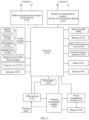
- FIG. 1 is a schematic circuit diagram of a possible reverse charging solution of an electronic device.
- the electronic device is a PC, including a power delivery (power delivery, PD) controller, a charging controller (also referred to as a charger), a battery, and two Type-C interfaces: an interface C1 and an interface C2.
- the interface C1 and the interface C2 are configured to be connected to an external device to implement some functions between the external device and the electronic device, such as a forward charging function (charging the electronic device through the external device) or a reverse charging function (charging the external device through the electronic device).
- the PD controller is configured for interactive communication of a charging protocol with the external device.
- the battery charging controller is configured to convert a voltage input by the external device through the interface C1 or the interface C2 into a suitable voltage, and then supply the voltage to a device and a battery to which the PC needs to supply power, so that forward charging is implemented.
- the PD controller is provided with a power input end Vin, a first power output end Vout1, and a second power output end Vout2.
- the power input end Vin is configured to receive a power supply voltage (such as 5 V) input by a buck conversion (BUCK) circuit to ensure normal operation of the PD controller.
- the power input end Vin is further connected to the first power output end Vout1 and the second power output end Vout2 respectively through a switch K1 and a switch K2 located inside the PD controller.
- the power input end Vin may be connected to the first power output end Vout1 and the second power output end Vout2, to output the power supply voltage input from the power input end Vin to the first power output end Vout1 and the second power output end Vout2, so that the PD controller has an external power supply capability.
- the first power output end Vout1 is connected to the interface C1
- the second power output end Vout2 is connected to the interface C2.
- the PD controller may provide voltage output to the interface C1 and the interface C2 respectively through the first power output end Vout1 and the second power output end Vout2 to implement the reverse charging function.
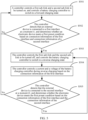
- FIG. 2 is a flowchart of reverse charging of the electronic device shown in FIG. 1 . The following steps are included.
- S201 An electronic device recognizes an access of an external device and performs CC handshake communication with the external device.
- the interface C1 when the interface C1 accesses the external device, the interface C1 sends an interrupt signal to the PD controller.
- the PD controller recognizes the access of the external device based on the interrupt signal, and then performs handshake communication with the external device in a configuration channel (configuration channel, CC) to determine types of the electronic device and the external device. If the type of the electronic device is an output device (also referred to as a source device) and the type of the external device is a receiving device (also referred to as a sink device), it indicates that the electronic device performs reverse charging on the external device. If the electronic device is the sink device and the external device is the output device, it indicates that the external device performs forward charging on the electronic device. In this example, the electronic device is the source device and the external device is the sink device.
- CC configuration channel
- a maximum current is 3A.
- the current output by the electronic device may be further limited.
- the electronic device in FIG. 1 can only provide a maximum charging power supply of 15 W (5 V/3 A), which cannot meet a high-power fast charging requirement expected by a user.
- FIG. 1 and FIG. 2 use two interfaces as an example to describe the problem that the electronic device cannot meet the high-power fast charging requirement expected by the user, in another embodiment, the electronic device including more or fewer interfaces still has the foregoing problem. The principle that causes the foregoing problem is similar and is not described again herein.
- the electronic device may be a device that supports a reverse charging function such as a power bank, a mobile phone, a tablet computer, a desktop computer, a laptop computer, a handheld computer, a notebook computer, an ultra-mobile personal computer (ultra-mobile personal computer, UMPC), a netbook, and the like.
- a specific form of the device is not specially limited in embodiments of this application.
- the function of the battery charging controller is to convert a power supply of the external device to the battery.
- some battery charging controllers further have a reverse output function that allows the battery to supply power to input ends of the battery charging controllers, so that output ends of the battery charging controllers may provide power output.
- a forward output function of the battery charging controller is used, so there is only one path on hardware and simultaneous existence of two functions cannot be supported.
- the reverse output function of the battery charging controller is used to allow the battery to provide power output through the battery charging controller to implement the reverse charging function. Since the electronic device implements reverse charging through a larger-capacity battery, a greater power output may be implemented and the high-power fast charging requirement of the user is met.
- FIG. 3 is a schematic structural diagram 1 of an electronic device according to some embodiments of this application.
- an electronic device 300 may include a processor 310, an external memory interface 320, an internal memory 321, a universal serial bus (universal serial bus, USB) interface 330, a charging management module 340, a power management module 341, a battery 342, an antenna 1, an antenna 2, a mobile communication module 350, a wireless communication module 360, an audio module 370, a speaker 370A, a phone receiver 370B, a microphone 370C, a headset jack 370D, a sensor module 380, a button 390, a motor 391, an indicator 392, a camera 393, a display screen 394, a subscriber identity module (subscriber identity module, SIM) card interface 396, and the like.
- SIM subscriber identity module
- the schematic structure in this embodiment constitutes no specific limitation on the electronic device 300.
- the electronic device 300 may include more or fewer components than those shown in the figure, or some components may be combined, or some components may be split, or components are arranged in different manners.
- the illustrated components may be implemented by hardware, software, or a combination of software and hardware.
- the processor 310 may include one or more processing units.
- the processor 310 may include an application processor (application processor, AP), a modem processor, a graphics processing unit (graphics processing unit, GPU), an image signal processor (image signal processor, ISP), a controller, a memory, a video codec, a digital signal processor (digital signal processor, DSP), a baseband processor, and/or a neural-network processing unit (neural-network processing unit, NPU).
- Different processing units may be independent components, or may be integrated into one or more processors.
- the controller may be a nerve center and a command center of the electronic device 300.
- the controller may generate an operation control signal based on an instruction operation code and a timing signal, and implement control on instruction fetching and instruction execution.
- a memory may be further configured in the processor 310, to store an instruction and data.
- the memory in the processor 310 is a cache memory.
- the memory may store an instruction or data that is recently used or to be cyclically used by the processor 310. If the processor 310 needs to use the instruction or the data again, the processor may directly invoke the instruction or the data from the memory, so that repeated access is avoided, and a waiting time of the processor 310 is reduced, thereby improving system efficiency.
- the processor 310 may include one or more interfaces.
- the interface may include an inter-integrated circuit (inter-integrated circuit, I2C) interface, an inter-integrated circuit sound (inter-integrated circuit sound, I2S) interface, a pulse code modulation (pulse code modulation, PCM) interface, a universal asynchronous receiver/transmitter (universal asynchronous receiver/transmitter, UART) interface, a mobile industry processor interface (mobile industry processor interface, MIPI), a general-purpose input/output (general-purpose input/output, GPIO) interface, a subscriber identity module (subscriber identity module, SIM) interface, and/or a universal serial bus (universal serial bus, USB) interface, and the like.
- I2C inter-integrated circuit
- I2S inter-integrated circuit sound
- PCM pulse code modulation
- PCM pulse code modulation
- UART universal asynchronous receiver/transmitter
- MIPI mobile industry processor interface
- GPIO general-purpose input/output
- FIG. 3 only illustrates a USB interface and a connection relationship of the USB interface.
- the electronic device 300 includes one or more USB interfaces 330.
- the USB interface 330 may be a Type-C interface or the like.
- a schematic interface connection relationship between the modules in embodiments is merely an example for description, and constitutes no limitation on the structure of the electronic device 300.
- the electronic device 300 may alternatively use an interface connection manner different from that in the foregoing embodiment, or use a combination of a plurality of interface connection manners.
- the charging management module 340 is configured to receive charging input from the charger.
- the charger may be a wireless charger or may be a wired charger.
- the charging management module 340 may receive charging input of the wired charger through the USB interface 330.
- the charging management module 340 may receive a wireless charging input by using a wireless charging coil of the electronic device 300.
- the charging management module 340 may supply power to the electronic device by using the power management module 341 while charging the battery 342.
- the PD module 343 is configured for charging protocol communication with the external device coupled to the electronic device 300 through the USB interface 330.
- the power management module 341 is configured to be connected to the battery 342, the charging management module 340, and the processor 310.
- the power management module 341 receives input from the battery 342 and/or the charging management module 340, to supply power to the processor 310, the internal memory 321, an external memory, the display screen 394, the camera 393, the wireless communication module 360, and the like.
- the power management module 341 may be further configured to monitor parameters such as a battery capacity, a cycle count of a battery, and a battery health state (leakage and impedance).
- the power management module 341 may alternatively be disposed in the processor 310.
- the power management module 341 and the charging management module 340 may also be disposed in a same device.
- a wireless communication function of the electronic device 300 may be implemented by using the antenna 1, the antenna 2, the mobile communication module 350, the wireless communication module 360, the modem processor, the baseband processor, and the like.
- the antenna 1 and the antenna 2 are configured to transmit and receive electromagnetic wave signals.
- Each antenna of the electronic device 300 may be configured to cover one or more communication frequency bands. Different antennas may further be reused to improve utilization of the antennas.
- the antenna 1 may be reused as a diversity antenna of a wireless local area network.
- the antenna may be used in combination with a tuning switch.
- the mobile communication module 350 may provide a solution to wireless communication such as 2G/3G/4G/3G applied to the electronic device 300.
- the mobile communication module 350 may include at least one filter, a switch, a power amplifier, a low noise amplifier (low noise amplifier, LNA), and the like.
- the mobile communication module 350 may receive an electromagnetic wave by using the antenna 1, perform processing such as filtering and amplification on the received electromagnetic wave, and send the electromagnetic wave to the modem processor for demodulation.
- the mobile communication module 350 may further amplify a signal modulated by the modem processor, and convert the signal into an electromagnetic wave by using the antenna 1 for radiation.
- at least some of functional modules of the mobile communication module 350 may be arranged in the processor 310.
- at least some functional modules of the mobile communication module 350 and at least some modules of the processor 310 may be disposed in a same component.
- the modem processor may include a modulator and a demodulator.
- the modulator is configured to modulate a to-be-sent low-frequency baseband signal into a medium-high-frequency signal.
- the demodulator is configured to demodulate the received electromagnetic wave signal into a low-frequency baseband signal. Then, the demodulator transmits the demodulated low-frequency baseband signal to the baseband processor for processing.
- the low-frequency baseband signal is processed by the baseband processor and then transmitted to an application processor.
- the application processor outputs a sound signal by using an audio device (not limited to the speaker 370A, the phone receiver 370B, or the like), or displays an image or a video by using the display screen 394.
- the modem processor may be an independent device.
- the modem processor may be independent of the processor 310, and the modem processor and the mobile communication module 350 or another functional module may be arranged in the same component.
- the wireless communication module 360 may provide a solution for wireless communication including a wireless local area network (wireless local area network, WLAN) (for example, a wireless fidelity (wireless fidelity, Wi-Fi) network), Bluetooth (Bluetooth, BT), and a global navigation satellite system (global navigation satellite system, GNSS), frequency modulation (frequency modulation, FM), a near field communication (near field communication, NFC) technology, an infrared (infrared, IR) technology, and the like to be applied to the electronic device 300.
- the wireless communication module 360 may be one or more components integrating at least one communication processor module.
- the wireless communication module 360 receives an electromagnetic wave via the antenna 2, performs frequency modulation and filtering on the electromagnetic wave signal, and sends the processed signal to the processor 310.
- the wireless communication module 360 may also receive a to-be-sent signal from the processor 310, perform frequency modulation and amplification on the to-be-sent signal, and convert the signal into an electromagnetic wave for radiation through the antenna 2.
- the antenna 1 and the mobile communication module 350 of the electronic device 300 are coupled, and the antenna 2 and the wireless communication module 360 are coupled, so that the electronic device 300 can communicate with a network and another device by using a wireless communication technology.
- the wireless communication technology may include a global system for mobile communications (global system for mobile communications, GSM), a general packet radio service (general packet radio service, GPRS), code division multiple access (code division multiple access, CDMA), wideband code division multiple access (wideband code division multiple access, WCDMA), time-division code division multiple access (time-division code division multiple access, TD-SCDMA), long term evolution (long term evolution, LTE), BT, a GNSS, a WLAN, NFC, FM, an IR technology, and/or the like.
- GSM global system for mobile communications
- GPRS general packet radio service
- code division multiple access code division multiple access
- CDMA wideband code division multiple access
- WCDMA wideband code division multiple access
- time-division code division multiple access time
- the GNSS may include a global positioning system (global positioning system, GPS), a global navigation satellite system (global navigation satellite system, GLONASS), a Beidou navigation satellite system (beidou navigation satellite system, BDS), a quasi-zenith satellite system (quasi-zenith satellite system, QZSS) and/or satellite-based augmentation systems (satellite based augmentation systems, SBAS).
- GPS global positioning system
- GLONASS global navigation satellite system
- Beidou navigation satellite system beidou navigation satellite system
- BDS Beidou navigation satellite system
- QZSS quasi-zenith satellite system
- SBAS satellite-based augmentation systems
- the electronic device 300 implements a display function by using the GPU, the display screen 394, the application processor, and the like.
- the GPU is a microprocessor for image processing, and is connected to the display screen 394 and the application processor.
- the GPU is configured to perform mathematical and geometric calculations and perform graphics rendering.
- the processor 310 may include one or more GPUs and execute program instructions to generate or change display information.
- the display screen 394 is configured to display an image and a video.
- the display screen 394 is sometimes referred to as a display module, and usually includes a display panel and a driving circuit for driving the display panel to display.
- the display panel may be a liquid crystal display (liquid crystal display, LCD), an organic light-emitting diode (organic light-emitting diode, OLED), an active-matrix organic light emitting diode (active-matrix organic light emitting diode, AMOLED), a flexible light-emitting diode (flex light-emitting diode, FLED), a Miniled, a MicroLed, a Micro-oLed, quantum dot light emitting diodes (quantum dot light emitting diodes, QLED), and the like.
- a driver module includes a display driver integrated circuit (display driver integrated circuit, DDIC) and an array formed by TFT devices.
- the electronic device 300 may implement a photographing function by using the ISP, the camera 393, the video codec, the GPU, the display screen 394, the application processor, and the like.
- the ISP is used to process data fed back by the camera 393. For example, during photographing, a shutter is opened, light is transferred to a camera photosensitive element by using a lens, an optical signal is converted into an electrical signal, and the camera photosensitive element transfers the electrical signal to the ISP for processing, to convert the electrical signal into an image visible to a naked eye.
- the ISP may also optimize noise point, brightness, and skin tone algorithms.
- the ISP may alternatively optimize parameters such as exposure and a color temperature of a photographing scenario.
- the ISP may be disposed in the camera 393.
- the camera 393 is configured to capture a static image or a video.
- An optical image of an object is generated through a lens and is projected to the photosensitive element.
- the photosensitive element may be a charge coupled device (charge coupled device, CCD) or a complementary metal-oxide-semiconductor (complementary metal-oxide-semiconductor, CMOS) phototransistor.
- CCD charge coupled device
- CMOS complementary metal-oxide-semiconductor
- the photosensitive element converts an optical signal into an electrical signal, and then transmits the electrical signal to the ISP to convert the electrical signal into a digital image signal.
- the ISP outputs the digital image signal to the DSP for processing.
- the DSP converts the digital image signal into a standard image signal in RGB and YUV formats.
- the electronic device 300 may include 1 or N cameras 393, and N is a positive integer greater than 1.
- the digital signal processor is configured to process a digital signal, and in addition to a digital image signal, may further process another digital signal.
- the digital signal processor is configured to perform Fourier transform and the like on frequency energy.
- the video codec is configured to compress or decompress a digital video.
- the electronic device 300 may support one or more video codecs. In this way, the electronic device 300 may play or record videos in a plurality of encoding formats, for example: moving picture experts group (moving picture experts group, MPEG) 1, MPEG 2, MPEG 3, and MPEG 4.
- MPEG moving picture experts group
- the NPU is a neural-network (neural-network, NN) computing processor that processes input information rapidly by referring to a structure of a biological neural network, for example, by referring to a transmission mode between human brain neurons, and can further perform self-learning continuously.
- the NPU may be used to implement an application such as intelligent cognition of the electronic device 300, for example, image recognition, facial recognition, voice recognition, and text understanding.
- the external memory interface 320 may be configured to be connected to an external storage card, for example, a micro SD card, to expand a storage capability of the electronic device 300.
- the external storage card communicates with the processor 310 by using the external memory interface 320, to implement a data storage function, such as storing a file such as music or a video in the external storage card.
- the internal memory 321 may be configured to store computer executable program code, where the executable program code includes instructions.
- the processor 310 runs the instructions stored in the internal memory 321, to perform various function applications and data processing of the electronic device 300. For example, in this embodiment of this application, the processor 310 may detect a folding angle (that is, an included angle between adjacent screens) of the display screen 394 (that is, a folding screen) by executing instructions stored in the internal memory 321, and displays display content (that is, an image) corresponding to the included angle in response to changes of the included angle.
- the internal memory 321 may include a program storage area and a data storage area.
- the program storage area may store an operating system, an application program required by at least one function (for example, a sound playback function and an image display function), and the like.
- the data storage area may store data (for example, audio data and an address book) and the like created when the electronic device 300 is used.
- the internal memory 321 may include a highspeed random access memory, or may include a non-volatile memory such as at least one magnetic disk memory, a flash memory, or a universal flash storage (universal flash storage, UFS).
- the electronic device 300 may implement an audio function such as music playing or recording by using the audio module 370, the speaker 370A, the phone receiver 370B, the microphone 370C, the headset jack 370D, the application processor, and the like. For example, implement a music playback function and a recording function.
- the audio module 370 is configured to convert digital audio information into an analog audio signal output, and is further configured to convert an analog audio input into a digital audio signal.
- the audio module 370 may be further configured to encode and decode an audio signal.
- the audio module 370 may be disposed in the processor 310, or some function modules of the audio module 370 are disposed in the processor 310.
- the speaker 370A also referred to as a "loudspeaker" is configured to convert an audio electrical signal into a sound signal.
- the electronic device 300 may be used to listen to music or answer a call in a hands-free mode by using the loudspeaker 370A.
- the phone receiver 370B also referred to as a "receiver” is configured to convert an audio electrical signal into a sound signal.
- the phone receiver 370B may be put close to a human ear, to receive a voice.
- the microphone 370C also referred to as a "mouthpiece” or a “megaphone”, is configured to convert a sound signal into an electrical signal.
- a user may speak with the mouth approaching the microphone 370C, to input a sound signal to the microphone 370C.
- At least one microphone 370C may be disposed in the electronic device 300.
- two microphones 370C may be disposed in the electronic device 300, to collect a sound signal and implement a noise reduction function. In some other embodiments, three, four, or more microphones 370C may be alternatively disposed in the electronic device 300, to collect a sound signal, implement noise reduction, recognize a sound source, implement a directional recording function, and the like.
- the headset jack 370D is configured to connect a wired headset.
- the headset jack 370D may be a USB interface 330, or may be a 3.3 mm open mobile terminal platform (open mobile terminal platform, OMTP) standard interface or cellular telecommunications industry association of the USA (cellular telecommunications industry association of the USA, CTIA) standard interface.
- OMTP open mobile terminal platform
- CTIA cellular telecommunications industry association of the USA
- the button 390 includes a power button, a volume button, and the like.
- the button 390 may be a mechanical button, or may be a touch-type button.
- the electronic device 300 may receive button input, and generate button signal input related to user setting and function control of the electronic device 300.
- the motor 391 may generate a vibration prompt.
- the motor 391 may be configured to provide a vibration prompt for an incoming call, and may be further configured to provide a touch vibration feedback.
- touch operations performed on different applications may correspond to different vibration feedback effects.
- touch operations performed on different areas of the display screen 394 the motor 391 may also correspond to different vibration feedback effects.
- Different application scenarios for example, a time reminder, information receiving, an alarm clock, and a game
- a touch vibration feedback effect may be further customized.
- the indicator 392 may be an indicator light, may be configured to indicate a charging state and a battery change, and may be further configured to indicate a message, a missed call, a notification, and the like.
- the SIM card interface 396 is configured to connect to a SIM card.
- the SIM card may be inserted into the SIM card interface 396 or plugged from the SIM card interface 396, to come into contact with or be separated from the electronic device 300.
- the electronic device 300 may support one or N SIM card interfaces. N is a positive integer greater than 1.
- the SIM card interface 396 can support a Nano SIM card, a Micro SIM card, a SIM card, and the like.
- a plurality of cards may be inserted into a same SIM card interface 396 at the same time.
- the plurality of cards may be of a same type or different types.
- the SIM card interface 396 may be further compatible with different types of SIM cards.
- the SIM card interface 396 may also be compatible with an external memory card.
- the electronic device 300 interacts with a network by using a SIM card, to implement functions such as a call and data communication.
- the electronic device 300 uses an eSIM, that is, an embedded SIM card.
- the eSIM card may be embedded in the electronic device 300 and cannot be separated from the electronic device 300.
- FIG. 4 is a schematic structural diagram 2 of an electronic device according to some embodiments of this application (the electronic device 300 shown in FIG. 3 ).
- the electronic device includes a battery, two charging interfaces (a first interface and a second interface respectively), a PD controller (the PD module 343 shown in FIG. 3 ), a battery charging controller, a first reverse charging link (all paths identified through the first reverse charging link in the figure form the first reverse charging link), two second reverse charging links: a first sub-link (all paths identified through the first sub-link in the figure form the first sub-link) and a second sub-link (all paths identified through the second sub-link in the figure form the second sub-link) respectively, and a controller (the controller in the processor 310 shown in FIG.
- the battery may be understood as the battery 342 shown in FIG. 3
- the PD controller may be understood as the PD module 343 shown in FIG. 3
- the controller may be understood as the controller in the processor 310 shown in FIG. 3 .
- the battery is configured to receive power input or provide power output.
- Both the first interface and the second interface are configured for the electronic device to be connected to the external device, such as a charger for charging the electronic device, or a mobile phone that needs to be charged.
- the first interface and the second interface may be Type-C interfaces. It should be understood that in this embodiment, the first interface and the second interface may be in the following three states: neither is connected to the external device, one is connected to the external device and the other is connected to the external device, or both are connected to the external device.
- the PD controller is coupled to the first interface and the second interface respectively (in FIG. 4 , an inter-integrated circuit (inter-integrated circuit, I2C) between the first interface and the PD controller and an I2C between the second interface and the PD controller show a coupling relationship), and the PD controller is configured to obtain connection information of the first interface and connection information of the second interface.
- the connection information indicates a connection status of the charging interface, and the connection status includes connected state or non-connected state.
- the connected state indicates that the charging interface (such as the first interface or the second interface) is connected to the external device, and the non-connected state indicates that the charging interface is not connected to the external device.
- connection information further indicates a device type of the external device when the charging interface is connected to the external device (that is, in the connected state).
- the device type includes a source device or a sink device.
- the source device is a device that provides power output
- the sink device is a device that receives power input.
- the first interface When the external device detaches from the first interface in response to an unplugging operation of the user, the first interface sends a first interrupt signal to the PD signal. After receiving the first interrupt signal, the PD controller determines, based on the first interrupt signal, that the first interface is in the non-connected state. When the external device accesses the first interface in response to an access operation of the user, the first interface sends a second interrupt signal to the PD signal. After receiving the second interrupt signal, the PD controller determines, based on the second interrupt signal, that the first interface is in the connected state. It should be noted that the PD controller has a function of performing charging protocol communication with the external device connected to the first interface.
- the PD controller when it is determined that the first interface is in the connected state, the PD controller establishes CC handshake communication with the external device to determine the device type of the external device.
- the external device and the electronic device are source devices and sink devices for each other, that is to say, one of the external device and the electronic device is the source device, and the other of the external device and the electronic device is the sink device.
- connection information indicates only the device type of the external device. It should be understood that in another embodiment, the connection information may also indicate the device type of the electronic device, or indicate the device types of the electronic device and the external device at the same time. Since the external device and the electronic device are source devices and sink devices for each other, after the device type of one of the devices is determined, the device type of the other device may be obtained. Embodiments of this application do not specifically limit an object of the device type indicated by the connection information.
- the PD controller has two power output ends: the first power output end Vout1 and the second power output end Vout2.
- the first power output end Vout1 and the second power output end Vout2 are configured to provide power output, such as 5 V/3 A output.
- the foregoing first interface is coupled to the first power output end Vout1 of the PD controller through the first sub-link
- the foregoing second interface is coupled to the second power output end Vout2 of the PD controller through the second sub-link. That is, one charging interface is connected to one power output end through one second reverse charging link.
- the electronic device may use the first power output end Vout1 of the PD controller to perform reverse charging on the external device connected to the first interface via the first sub-link; and may further use the second power output end Vout2 of the PD controller to perform reverse charging on the external device connected to the second interface via the second sub-link.
- the first sub-link and the second sub-link may be understood as links from the USB interface 330 to the PD module 343 shown in FIG. 3 .
- the first sub-link includes a first switching element Q1; and the second sub-link includes a second switching element Q2.
- a first end of the first switching element Q1 is coupled to the first interface, and a second end of the first switching element Q1 is coupled to the first power output end 1 Vout1.
- a first end of the second switching element Q2 is coupled to the second interface, and a second end of the second switching element Q2 is coupled to the second power output end Vout2.
- the first switching element Q1 and the second switching element Q2 may be N-type transistors.
- the first ends of the first switching element Q1 and the second switching element Q2 may be sources of the transistors, and the second ends of the first switching element Q1 and the second switching element Q2 may be drains of the transistors.
- the first switching element Q1 and the second switching element Q2 may be switching chips.
- the switching element when the switching element is a transistor, the first end of the switching element refers to the source of the transistor, the second end of the switching element refers to the drain of the transistor, and the third end of the switching element refers to a gate of the transistor. Details are not described again.
- the first sub-link and the second sub-link may be on and off, thereby switching the reverse charging link of the electronic device.
- the foregoing first interface and the second interface are further coupled to the battery through the first reverse charging link.
- the first reverse charging link is coupled to the battery charging controller.
- the battery charging controller includes a forward charging state (that is, the foregoing forward output function) and a reverse charging state (that is, the foregoing reverse output function).
- the fifth end D5 of the battery charging controller is configured to receive an external control instruction. In response to the external control instruction, the battery charging controller may switch to the forward charging state or the reverse charging state. When the battery charging controller operates in the reverse charging state, the battery charging controller may control the first reverse charging link to perform reverse charging.
- the electronic device may use the battery to perform reverse charging on the external device connected to the first interface and the second interface via the first reverse charging link.
- the battery charging controller When the battery charging controller operates in the forward charging state, the battery charging controller may control the first reverse charging link to perform forward charging.
- the electronic device may use the first interface and the second interface to receive the power input provided by the external device, and then perform forward charging on the battery through the first reverse charging link.
- power may also be supplied to other operating components of the electronic device.
- a model of the foregoing battery charging controller may be BQ25713. This model of battery charging controller may operate in two states: the forward charging state and the reverse charging state.
- the first reverse charging link may be understood as the link from the USB interface 330 to the battery 342 shown in FIG. 3
- the battery charging controller may be understood as the charging management module 340 shown in FIG. 3 .
- the controller may be an embed controller (embed controller, EC).
- a first end P1 (such as GPIO1) of the controller is coupled to the fifth end D5 of the battery charging controller, a second end P2 (such as GPIO 1) of the controller is coupled to the first sub-link, a third end P3 of the controller (such as GPIO 1) is coupled to the second sub-link, and a fourth end P4 of the controller is coupled to the PD controller (the I2C between the PD controller and the controller in the figure illustrates the coupling relationship).
- the controller is configured to obtain the connection information of the first interface and the connection information of the second interface through the fourth end P4 of the controller, and is further configured to control, when determining that the electronic device meets a first preset condition based on the connection information of the first interface and the connection information of the second interface, the battery charging controller to switch to the reverse charging state for performing reverse charging through the first end P1 of the controller, and to control the target link to be turned off through the second end P2 and the third end P3 of the controller.
- the first preset condition includes that the electronic device is in a non-forward charging state, and the first interface and/or the second interface are connected to the sink device.
- the target link includes a second reverse charging link corresponding to the charging interface connected to the sink device in the first interface and the second interface. That is to say, if only the first interface is connected to the sink device, the target link includes the first sub-link; if only the second interface is connected to the sink device, the target link includes the second sub-link; and if the first interface and the second interface are each connected to the sink device, the target link includes the first sub-link and the second sub-link.
- the second end P2 of the controller is coupled to the third end of the first switching element Q1, and the third end P3 of the controller is coupled to the third end of the second switching element Q2.
- the controller is configured to output a first control instruction through the second end P2 of the controller, and output a second control instruction through the third end P3 of the controller.
- the first control instruction and the second control instruction respectively instructs the first switching element Q1 and the second switching element Q2 to switch to the on state or the off state.
- the first switching element Q1 and the second switching element Q2 When the first switching element Q1 and the second switching element Q2 switch to the on state, the first sub-link and the second sub-link are turned off; and when the first switching element Q1 and the second switching element Q2 switch to the off state, the first sub-link and the second sub-link are turned on.
- the third ends of the first switching element Q1 and the second switching element Q2 may be gates of the N-type transistor.
- the electronic device further includes a third switching element Q3.
- the first end P1 of the controller is coupled to a third end of the third switching element Q3, a second end of the third switching element Q3 is coupled to the fifth end D5 of the battery charging controller, and a first end of the third switching element Q3 is coupled to the reference ground.
- the controller is configured to output a third control instruction through the first end P 1 of the controller.
- the third control instruction instructs the third switching element Q3 to switch to the on state or the off state, so that the third switching element Q3 outputs the foregoing external control instruction.
- the third switching element Q3 When the third switching element Q3 switches to the on state, the third switching element Q3 sends a first external control instruction, and the first external control instruction instructs the battery charging controller to switch to the reverse charging state; and when the third switching element switches to the off state, the third switching element Q3 sends a second external control instruction, and the second external control instruction instructs the battery charging controller to switch to the forward charging state.
- the third switching element Q3 For the specific implementation of the third switching element Q3, reference may be made to the specific implementation of the first switching element Q1, which will not be described again herein.
- the status switching of the battery charging controller is implemented, thereby realizing the switching of the reverse charging link of the electronic device. It should be noted that since a status control end of the battery charging controller is in a high-impedance state, the first end of the third switching element Q3 further needs to be connected to a pull-up resistor R.
- the electronic device is in the forward charging state means that the electronic device receives power input provided by the external device to charge the battery; and that the electronic device is not in the forward charging state means that the electronic device does not receive power input provided by the external device to charge the battery.
- any one of the first interface and the second interface of the electronic device is connected to the external device and receives the power input of the external device, or both interfaces are connected to external devices and simultaneously receives the power input of the external devices connected to the two interfaces respectively, so that the electronic device may be in the forward charging state.
- the electronic device may not be in the forward charging state.
- the electronic device receives the power input provided by the external device connected to the charging interface. Conversely, if the charging interface of the electronic device is not connected to the source device, the electronic device does not receive the power input of the external device. Based on this, when the first interface and/or the second interface are connected to the source device (that is, one of the two charging interfaces or both are connected to the source device), it means that the electronic device is in the forward charging state; and when neither the first interface nor the second interface is connected to the source device, it means that the electronic device is not in the forward charging state.
- first interface and/or the second interface are connected to the source device includes one of the following situations:
- the controller may determine whether the first interface and the second interface meet one of the foregoing three situations for outputting based on the connection information of the first interface and the connection information of the second interface. If so, it is determined that the first preset condition is met; and if not, it is determined that the first preset condition is not met.
- the foregoing three situations they are all device types of the external devices connected to the charging interface. Therefore, if the device type indicated by the connection information is the device type of the electronic device, another device type different from the device type indicated by the connection information may be determined as the device type of the external device connected to the charging interface.
- the reverse output function of the battery charging controller is used to allow the battery to provide power output to the sink device connected to the charging interface through the battery charging controller to implement the reverse charging function. Since the electronic device implements reverse charging through a larger-capacity battery, a greater power output may be implemented and the high-power fast charging requirement of the user is met.
- a common reverse charging solution in the industry is to add a PD controller and a BUCK circuit on the basis of FIG. 1 , which are used alone to provide high-power fast charging to the external device.
- Adding the PD controller and the BUCK circuit is equivalent to a small charging system, and in this case, the software configuration is more complicated, debugging is more difficult, and the research and development investment cost is much higher.
- the embodiment shown in FIG. 1 the embodiment shown in FIG.
- the controller is further configured to control, when determining that the electronic device meets a second preset condition, the battery charging controller to switch to the forward charging state and control the target link to be turned on, where the second preset condition includes that the electronic device is in the forward charging state.
- the battery charging controller has the forward output function and the reverse output function. Since only the forward output function of the battery charging controller is currently used, there is only one path in a hardware design, and the two functions cannot be supported at the same time. Based on this, in this embodiment, to give priority to ensuring the normal operation of the electronic device, when the electronic device is in the forward charging state, the battery charging controller is controlled to switch to the forward charging state to ensure the forward charging function of the electronic device. At the same time, the target link is controlled to be turned on, so that the PD controller provides power output and implement reverse charging, thereby meeting the user requirement of using the electronic device to reversely charge the external device.
- the second preset condition may also include one of the following situations:
- the electronic device when not charging (neither forward charging nor reverse charging), the electronic device is adjusted by default to a ready state in which the forward charging function is provided, so that when the forward charging is required, the forward charging is performed without link switching, which is beneficial to ensuring user experience of a commonly used forward charging function of the electronic device.
- the second preset condition and the first preset condition are complementary and cover all statuses of the first interface and the second interface of the electronic device. Therefore, when the electronic device does not meet the first preset condition, the second preset condition is met; and when the electronic device does not meet the second preset condition, the first preset condition is met.
- the situation in which both the first interface and the second interface are in the non-connected state may also be regarded as the foregoing first preset condition, which is not specifically limited in this embodiment of this application.
- the target link further includes another link in the two second reverse charging links other than the second reverse charging link corresponding to the charging interface connected to the sink device. That is to say, when the controller determines that the electronic device meets the first preset condition, all second reverse charging links are controlled to be turned off; and when the controller determines that the electronic device meets the second preset condition, all second reverse charging links are controlled to be turned on.
- the reverse charging is performed by the second reverse charging link.
- the first interface is connected to the source device for the forward charging
- the second interface is connected to the sink device for the reverse charging
- an internal switch is controlled to be turned off to cut off the path on which the first sub-link provides power output to the first interface. Based on this, when the electronic device meets the second preset condition, even if the two second reverse charging links are controlled to be turned on at the same time, the PD controller cannot provide power output to the first interface through the first sub-link, thereby avoiding affecting the forward charging process of the first interface.
- the target link only includes the second reverse charging link corresponding to the charging interface connected to the sink device
- all second reverse charging links are controlled to be turned off
- all second reverse charging links are controlled to be turned on, without recognizing the charging interface connected to the sink device, and controlling the corresponding second reverse charging link to be turned off or on.
- this embodiment is beneficial to reducing the control complexity.
- connection information further indicates a current parameter and a voltage parameter required by the external device when the external device is the sink device.
- the fifth end P5 of the controller is further coupled to a sixth end D6 of the battery charging controller (the I2C between the controller and the battery charging controller in the figure illustrates the coupling relationship).
- the controller is further configured to control, based on the current parameter and the voltage parameter, a current and a voltage of the battery charging controller during reverse charging.
- the external device informs the electronic device of the current parameter and the voltage parameter that are required by the electronic device.
- the PD controller receives the current parameter and the voltage parameter through the I2C between the first interface and the second interface, and reports the current parameter and the voltage parameter to the controller. Based on the current parameter and the voltage parameter, the controller may configure a register of the battery charging controller to control the current and the voltage during reverse charging of the battery charging controller.
- the electronic device using the current and the voltage when the battery charging controller is controlled to perform high-power reverse charging is not reached in one step, but a process of gradual increase.
- the electronic device when the electronic device starts reverse charging, the electronic device first configures the battery charging controller to reversely output a voltage of 5V, and the current parameter initially informed by the external device is usually a maximum of 3A.
- the external device continues to inform the required voltage parameter and the current parameter.
- the PD controller reports the voltage parameter and the current parameter to the controller, and the controller reconfigures current and voltage parts in the register of the battery charging controller to implement the high-power reverse charging function.
- the controller is further configured to: determine, before reverse charging, whether output power of the electronic device is greater than a preset threshold. When the output power of the electronic device is greater than the preset threshold, the battery charging controller is controlled to switch to the reverse charging state for reverse charging.
- the controller may obtain the maximum power output (that is, output power) that the electronic device may provide by reading the current and voltage parts in the register of the battery charging controller.
- the preset threshold that is, the power of the electronic device is sufficient
- the power output is provided to the outside, which is beneficial to ensuring the normal operation of the electronic device.
- a size of the preset threshold may be adjusted based on actual requirements.
- the first reverse charging link is provided with a fourth switching element Q4 and a fifth switching element Q5 on a link between a node X1 and the first interface
- the first reverse charging link is provided with a sixth switching element Q6 and a seventh switching element Q7 on a link between the node X1 and the second interface.
- a first end of the fourth switching element Q4 is coupled to the first interface
- a second end of the fourth switching element Q4 is coupled to a second end of the fifth switching element Q5
- a first end of the fifth switching element Q5 is coupled to the battery charging controller
- a third end of the fourth switching element Q4 and a third end of the fifth switching element Q5 are coupled to the PD controller.
- a first end of the sixth switching element Q6 is coupled to the first interface, a second end of the sixth switching element Q6 is coupled to a second end of the seventh switching element Q7, a first end of the seventh switching element Q7 is coupled to the battery charging controller, and a third end of the sixth switching element Q6 and a third end of the seventh switching element Q7 are coupled to the PD controller.
- the PD controller is coupled to the fourth switching element Q4, the fifth switching element Q5, the sixth switching element Q6, and the seventh switching element Q7 respectively, and is configured to control, after the CC handshake is successful, the fourth switching element Q4, the fifth switching element Q5, the sixth switching element Q6, and the seventh switching element Q7 to be turned on to implement the conduction of the first reverse charging link.
- the fourth switching element Q4, the fifth switching element Q5, the sixth switching element Q6, and the seventh switching element Q7 reference may be made to the specific implementation of the first switching element Q1, which will not be described again herein.
- the purpose of arranging two switching devices on each of the link of the first reverse charging link that is located between the node X1 and the first interface and the link of the first reverse charging link that is located between the node X1 and the second interface is to prevent leakage.
- one switching element may also be provided, which is not specifically limited in this embodiment of this application.
- the electronic device further includes an eighth switching element Q8.
- a first end of the eighth switching element Q8 is coupled to a seventh end D7 of the battery charging controller, and a second end of the eighth switching element Q8 is coupled to the battery. That is to say, the second end D2 of the battery charging controller is coupled to the battery through the eighth switching element Q8.
- a third end of the eighth switching element Q8 is coupled to the fifth end of the battery charging controller.
- the battery charging controller is configured to control the on and off of the eighth switching element Q8 through the fifth end D5 of the battery charging controller to control the battery for power output or power input.
- the eighth switching element Q8 may be a P-type transistor or a switching chip.
- the first reverse charging link includes a ninth switching element Q9, a tenth switching element Q10, an eleventh switching element Q 11, and a twelfth switching element Q12.
- a second end of the ninth switching element Q9 is coupled to the first interface and the second interface respectively, and a first end of the ninth switching element Q9 is coupled to a second end of the tenth switching element Q 10.
- a first end of the tenth switching element Q10 is coupled to ground.
- a second end of the eleventh switching element Q11 is coupled to the battery, and a first end of the eleventh switching element Q11 is coupled to a second end of the twelfth switching element Q12.
- a first end of the twelfth switching element Q12 is coupled to ground.
- first end of the ninth switching element Q9 and the second end of the tenth switching element Q 10 are further coupled to the first end of the eleventh switching element Q11 and the second end of the twelfth switching element Q12 through an inductor L to form the path of the first reverse charging link.
- a third end of the ninth switching element Q9 is coupled to the first end D1 of the battery charging controller, a third end of the tenth switching element Q10 is coupled to the second end D2 of the battery charging controller, a third end of the eleventh switching element Q11 is coupled to the third end D3 of the battery charging controller, and a third end of the twelfth switching element Q12 is coupled to the fourth end D4 of the battery charging controller.
- the first end D 1 of the battery charging controller may output a first driving instruction to the ninth switching element Q9
- the second end D2 of the battery charging controller may output a second driving instruction to the tenth switching element Q10
- the first driving instruction and the second driving instruction drive the ninth switching element Q9 and the tenth switching element Q10 to be alternately turned on and off at a high speed, thereby controlling the first reverse charging link to perform forward charging.
- the third end D3 of the battery charging controller may output a third driving instruction to the eleventh switching element Q11
- the second end D2 of the battery charging controller may output a fourth driving instruction to the twelfth switching element Q12
- the third driving instruction and the fourth driving instruction drive the eleventh switching element Q11 and the twelfth switching element Q12 to be alternately turned on and off at a high speed, thereby controlling the first reverse charging link to perform reverse charging.
- a set of switches of the ninth switching element Q9 and the tenth switching element Q10 may also be used to achieve voltage boosting, and a set of switches of the eleventh switching element Q11 and the twelfth switching element Q12 are used to achieve voltage reduction, which is not specifically limited in this embodiment of this application.
- the first driving instruction and the second driving instruction are pulse width modulation (Pulse Width Modulation, PWM) signals respectively.
- PWM Pulse Width Modulation
- FIG. 5 is a flowchart of a charging control method according to an embodiment of this application. This embodiment is based on the electronic device shown in FIG. 4 and is described by using an example in which the first interface accesses the external device at a moment t1 and the second interface accesses the external device at a moment t2.
- the first preset condition and the second preset condition are either one or the other.
- the charging control method includes:
- S501 A controller controls a first sub-link and a second sub-link to be turned on, and controls a battery charging controller to switch to a forward charging state.
- the reverse output function of the battery charging controller is turned off, and a reverse charging path from the PD controller to the first interface and the second interface is turned on to ensure user experience of a commonly used forward charging function.
- the controller may achieve the foregoing purpose by pulling up P1, P2, and P3.
- S502 The controller detects that an external device is connected to a first interface at a moment t1, and determines whether an electronic device meets a first preset condition based on connection information of the first interface and connection information of a second interface.
- S503 The controller controls the first sub-link and the second sub-link to be turned off, and controls the battery charging controller to switch to a reverse charging state.
- the controller may achieve the foregoing purpose by pulling down P1, P2, and P3.
- S504 The controller controls a current and a voltage of the battery charging controller during reverse charging based on the connection information of the first interface.
- S505 The controller detects that the external device is connected to the second interface at a moment t2, and determines whether the electronic device meets the first preset condition based on the connection information of the first interface and the connection information of the second interface.
- FIG. 4 and FIG. 5 use an example in which the electronic device includes two charging interfaces for description, in another embodiment, the electronic device may include more or fewer charging interfaces, and a specific implementation is similar to that of the two charging interfaces. The difference is that a quantity of power output ends of the second reverse charging link and the PD controller, and a quantity of branches from the node X1 to the charging interface on the first reverse charging link are consistent with that of charging interfaces, and one charging interface is connected to one power output end of the PD controller through one second reverse charging link, and is also coupled to the battery through the branch from the charging interface to the node X1 on the first reverse charging link. Embodiments of this application will not be described in detail.
Landscapes
- Engineering & Computer Science (AREA)
- Power Engineering (AREA)
- Manufacturing & Machinery (AREA)
- Chemical & Material Sciences (AREA)
- Chemical Kinetics & Catalysis (AREA)
- Electrochemistry (AREA)
- General Chemical & Material Sciences (AREA)
- Charge And Discharge Circuits For Batteries Or The Like (AREA)
Applications Claiming Priority (2)
| Application Number | Priority Date | Filing Date | Title |
|---|---|---|---|
| CN202210725580.5A CN116054299B (zh) | 2022-06-24 | 2022-06-24 | 电子设备 |
| PCT/CN2023/092588 WO2023246340A1 (zh) | 2022-06-24 | 2023-05-06 | 电子设备 |
Publications (2)
| Publication Number | Publication Date |
|---|---|
| EP4407831A1 true EP4407831A1 (de) | 2024-07-31 |
| EP4407831A4 EP4407831A4 (de) | 2025-07-09 |
Family
ID=86120568
Family Applications (1)
| Application Number | Title | Priority Date | Filing Date |
|---|---|---|---|
| EP23825990.7A Pending EP4407831A4 (de) | 2022-06-24 | 2023-05-06 | Elektronische vorrichtung |
Country Status (4)
| Country | Link |
|---|---|
| US (1) | US20250055297A1 (de) |
| EP (1) | EP4407831A4 (de) |
| CN (4) | CN117833394A (de) |
| WO (1) | WO2023246340A1 (de) |
Families Citing this family (3)
| Publication number | Priority date | Publication date | Assignee | Title |
|---|---|---|---|---|
| CN117833394A (zh) * | 2022-06-24 | 2024-04-05 | 荣耀终端有限公司 | 电子设备 |
| CN119448470A (zh) * | 2023-08-07 | 2025-02-14 | 华为技术有限公司 | 一种充电方法和终端设备 |
| WO2026065168A1 (zh) * | 2024-09-27 | 2026-04-02 | 荣耀终端股份有限公司 | 放电模组及其控制方法、电子设备 |
Family Cites Families (13)
| Publication number | Priority date | Publication date | Assignee | Title |
|---|---|---|---|---|
| CN106026247A (zh) * | 2016-06-17 | 2016-10-12 | 上海与德通讯技术有限公司 | 充电设备及其充电方法 |
| US10594151B2 (en) * | 2016-12-14 | 2020-03-17 | Shenzhen Lvsun Electronics Technology Co., Ltd | Conversion device for quick charger and method for realizing charging conversion |
| CN108964182B (zh) * | 2018-07-17 | 2020-12-04 | 北京小米移动软件有限公司 | 反向充电设备、反向充电电流的调节方法及装置 |
| CN110829523B (zh) * | 2019-10-31 | 2021-12-31 | 华为技术有限公司 | 一种电子设备及反向充电方法 |
| CN112928787B (zh) * | 2019-12-06 | 2024-07-09 | 北京小米移动软件有限公司 | 充电电路、电子设备、充电控制方法及装置 |
| CN116742740B (zh) * | 2020-06-30 | 2024-06-11 | 荣耀终端有限公司 | 一种充电装置及电子设备 |
| CN121584812A (zh) * | 2020-07-27 | 2026-02-27 | 华为技术有限公司 | 充电装置、电子设备、充电系统及充电方法 |
| EP4187750A4 (de) * | 2020-10-23 | 2024-03-06 | Samsung Electronics Co., Ltd. | Schnellladeverfahren und elektronische vorrichtung |
| CN114597983B (zh) * | 2020-12-04 | 2026-04-21 | 华为技术有限公司 | 一种无线充电电路及系统、电子设备及控制方法 |
| CN112564075B (zh) * | 2020-12-21 | 2023-05-23 | 张成君 | 双向充电线结构 |
| CN113162161A (zh) * | 2021-04-07 | 2021-07-23 | 深圳维普创新科技有限公司 | 一种基于Type-c接口的充放电电路控制方法、电路以及控制器 |
| CN114498865B (zh) * | 2022-04-14 | 2022-09-20 | 荣耀终端有限公司 | 充电电路、充电控制方法和电子设备 |
| CN117833394A (zh) * | 2022-06-24 | 2024-04-05 | 荣耀终端有限公司 | 电子设备 |
-
2022
- 2022-06-24 CN CN202311668868.4A patent/CN117833394A/zh active Pending
- 2022-06-24 CN CN202210725580.5A patent/CN116054299B/zh active Active
-
2023
- 2023-05-06 CN CN202380024480.2A patent/CN118830162B/zh active Active
- 2023-05-06 CN CN202411331344.0A patent/CN119362633A/zh active Pending
- 2023-05-06 EP EP23825990.7A patent/EP4407831A4/de active Pending
- 2023-05-06 US US18/708,469 patent/US20250055297A1/en active Pending
- 2023-05-06 WO PCT/CN2023/092588 patent/WO2023246340A1/zh not_active Ceased
Also Published As
| Publication number | Publication date |
|---|---|
| CN116054299A (zh) | 2023-05-02 |
| US20250055297A1 (en) | 2025-02-13 |
| CN117833394A (zh) | 2024-04-05 |
| WO2023246340A1 (zh) | 2023-12-28 |
| EP4407831A4 (de) | 2025-07-09 |
| CN118830162A (zh) | 2024-10-22 |
| CN119362633A (zh) | 2025-01-24 |
| CN118830162B (zh) | 2025-08-05 |
| CN116054299B (zh) | 2023-11-10 |
Similar Documents
| Publication | Publication Date | Title |
|---|---|---|
| EP4407831A1 (de) | Elektronische vorrichtung | |
| US11703960B2 (en) | Air mouse mode implementation method and related device | |
| EP4050754B1 (de) | Stromversorgungssystem und elektronische vorrichtung | |
| US12603068B2 (en) | Screen brightness adjustment method, electronic device, and computer-readable storage medium | |
| CN114498804B (zh) | 用于开机或唤醒系统的电子设备和控制电路 | |
| JP2023510259A (ja) | モバイル端末の消費電力を削減するための方法およびモバイル端末 | |
| WO2021052170A1 (zh) | 马达振动控制方法及电子设备 | |
| CN113473013A (zh) | 图像美化效果的显示方法、装置和终端设备 | |
| CN113672534B (zh) | 终端设备和开关电路 | |
| CN115113716A (zh) | 一种息屏显示参数的调节方法和终端设备 | |
| CN113656099B (zh) | 一种应用快捷启动方法、装置和终端设备 | |
| CN113923528B (zh) | 屏幕共享方法、终端和存储介质 | |
| CN113099734B (zh) | 天线切换方法及装置 | |
| US12219235B2 (en) | Electronic device and camera module | |
| CN117134009A (zh) | 充电方法及电子设备 | |
| CN116149581A (zh) | 一种多窗口对象投屏方法、电子设备及系统 | |
| EP4451536A1 (de) | Schaltkondensatorwandler (sc) und elektronische vorrichtung | |
| CN219834364U (zh) | 音频电路和终端设备 | |
| EP4648045A1 (de) | Tonaufnahmeverfahren und elektronische vorrichtung | |
| CN121919154A (zh) | 使能控制电路和电子设备 | |
| HK40080342B (zh) | 电子设备和摄像头模组 | |
| WO2026016626A1 (zh) | 电子设备运行状态的调整方法、电子设备和计算机可读存储介质 | |
| CN116054307A (zh) | 电源控制系统及电子设备 | |
| CN120256031A (zh) | 图像帧的渲染方法、装置和终端设备 |
Legal Events
| Date | Code | Title | Description |
|---|---|---|---|
| STAA | Information on the status of an ep patent application or granted ep patent |
Free format text: STATUS: THE INTERNATIONAL PUBLICATION HAS BEEN MADE |
|
| PUAI | Public reference made under article 153(3) epc to a published international application that has entered the european phase |
Free format text: ORIGINAL CODE: 0009012 |
|
| STAA | Information on the status of an ep patent application or granted ep patent |
Free format text: STATUS: REQUEST FOR EXAMINATION WAS MADE |
|
| 17P | Request for examination filed |
Effective date: 20240425 |
|
| AK | Designated contracting states |
Kind code of ref document: A1 Designated state(s): AL AT BE BG CH CY CZ DE DK EE ES FI FR GB GR HR HU IE IS IT LI LT LU LV MC ME MK MT NL NO PL PT RO RS SE SI SK SM TR |
|
| A4 | Supplementary search report drawn up and despatched |
Effective date: 20250610 |
|
| RIC1 | Information provided on ipc code assigned before grant |
Ipc: H02J 7/34 20060101ALI20250603BHEP Ipc: H02J 7/00 20060101AFI20250603BHEP |
|
| DAV | Request for validation of the european patent (deleted) | ||
| DAX | Request for extension of the european patent (deleted) | ||
| GRAP | Despatch of communication of intention to grant a patent |
Free format text: ORIGINAL CODE: EPIDOSNIGR1 |
|
| STAA | Information on the status of an ep patent application or granted ep patent |
Free format text: STATUS: GRANT OF PATENT IS INTENDED |
|
| INTG | Intention to grant announced |
Effective date: 20251223 |
|
| GRAS | Grant fee paid |
Free format text: ORIGINAL CODE: EPIDOSNIGR3 |
|
| GRAA | (expected) grant |
Free format text: ORIGINAL CODE: 0009210 |
|
| STAA | Information on the status of an ep patent application or granted ep patent |
Free format text: STATUS: THE PATENT HAS BEEN GRANTED |