EP4407797A1 - Rekonfigurierbare intelligente oberfläche und drahtloses kommunikationsnetzwerk - Google Patents
Rekonfigurierbare intelligente oberfläche und drahtloses kommunikationsnetzwerk Download PDFInfo
- Publication number
- EP4407797A1 EP4407797A1 EP23154064.2A EP23154064A EP4407797A1 EP 4407797 A1 EP4407797 A1 EP 4407797A1 EP 23154064 A EP23154064 A EP 23154064A EP 4407797 A1 EP4407797 A1 EP 4407797A1
- Authority
- EP
- European Patent Office
- Prior art keywords
- antenna elements
- intelligent surface
- reconfigurable intelligent
- wireless communication
- communication network
- Prior art date
- Legal status (The legal status is an assumption and is not a legal conclusion. Google has not performed a legal analysis and makes no representation as to the accuracy of the status listed.)
- Pending
Links
- 238000004891 communication Methods 0.000 title claims abstract description 39
- 230000010287 polarization Effects 0.000 claims abstract description 49
- 239000002184 metal Substances 0.000 claims description 6
- 230000001902 propagating effect Effects 0.000 claims description 3
- 239000010410 layer Substances 0.000 description 31
- 238000002310 reflectometry Methods 0.000 description 8
- 238000004519 manufacturing process Methods 0.000 description 6
- 239000000758 substrate Substances 0.000 description 6
- 239000000463 material Substances 0.000 description 4
- 239000012790 adhesive layer Substances 0.000 description 3
- 238000005388 cross polarization Methods 0.000 description 3
- 239000012777 electrically insulating material Substances 0.000 description 3
- 238000005516 engineering process Methods 0.000 description 3
- 238000000034 method Methods 0.000 description 3
- 230000005540 biological transmission Effects 0.000 description 2
- 238000004590 computer program Methods 0.000 description 1
- 239000004020 conductor Substances 0.000 description 1
- 230000003993 interaction Effects 0.000 description 1
- 230000015654 memory Effects 0.000 description 1
Images


Classifications
-
- H—ELECTRICITY
- H01—ELECTRIC ELEMENTS
- H01Q—ANTENNAS, i.e. RADIO AERIALS
- H01Q1/00—Details of, or arrangements associated with, antennas
- H01Q1/52—Means for reducing coupling between antennas; Means for reducing coupling between an antenna and another structure
- H01Q1/526—Electromagnetic shields
-
- H—ELECTRICITY
- H01—ELECTRIC ELEMENTS
- H01Q—ANTENNAS, i.e. RADIO AERIALS
- H01Q15/00—Devices for reflection, refraction, diffraction or polarisation of waves radiated from an antenna, e.g. quasi-optical devices
- H01Q15/0006—Devices acting selectively as reflecting surface, as diffracting or as refracting device, e.g. frequency filtering or angular spatial filtering devices
- H01Q15/0013—Devices acting selectively as reflecting surface, as diffracting or as refracting device, e.g. frequency filtering or angular spatial filtering devices said selective devices working as frequency-selective reflecting surfaces, e.g. FSS, dichroic plates, surfaces being partly transmissive and reflective
- H01Q15/002—Devices acting selectively as reflecting surface, as diffracting or as refracting device, e.g. frequency filtering or angular spatial filtering devices said selective devices working as frequency-selective reflecting surfaces, e.g. FSS, dichroic plates, surfaces being partly transmissive and reflective said selective devices being reconfigurable or tunable, e.g. using switches or diodes
-
- H—ELECTRICITY
- H01—ELECTRIC ELEMENTS
- H01Q—ANTENNAS, i.e. RADIO AERIALS
- H01Q15/00—Devices for reflection, refraction, diffraction or polarisation of waves radiated from an antenna, e.g. quasi-optical devices
- H01Q15/0006—Devices acting selectively as reflecting surface, as diffracting or as refracting device, e.g. frequency filtering or angular spatial filtering devices
- H01Q15/0013—Devices acting selectively as reflecting surface, as diffracting or as refracting device, e.g. frequency filtering or angular spatial filtering devices said selective devices working as frequency-selective reflecting surfaces, e.g. FSS, dichroic plates, surfaces being partly transmissive and reflective
- H01Q15/0026—Devices acting selectively as reflecting surface, as diffracting or as refracting device, e.g. frequency filtering or angular spatial filtering devices said selective devices working as frequency-selective reflecting surfaces, e.g. FSS, dichroic plates, surfaces being partly transmissive and reflective said selective devices having a stacked geometry or having multiple layers
-
- H—ELECTRICITY
- H01—ELECTRIC ELEMENTS
- H01Q—ANTENNAS, i.e. RADIO AERIALS
- H01Q3/00—Arrangements for changing or varying the orientation or the shape of the directional pattern of the waves radiated from an antenna or antenna system
- H01Q3/44—Arrangements for changing or varying the orientation or the shape of the directional pattern of the waves radiated from an antenna or antenna system varying the electric or magnetic characteristics of reflecting, refracting, or diffracting devices associated with the radiating element
- H01Q3/46—Active lenses or reflecting arrays
Definitions
- the invention generally relates to a reconfigurable intelligent surface for improving network performance.
- the invention further relates to a wireless communication network.
- RISs Reconfigurable intelligent surfaces
- such RISs comprise a plurality of antenna elements, wherein the individual antenna elements can be configured such that desired reflection properties of the RIS are obtained.
- At least one resistance of the individual antenna elements and/or at least one capacitance of the individual antenna elements may be adapted in order to obtain the desired reflection properties of the RIS.
- the object of the present invention is to provide a dual-polarized RIS that is easier and more cost-efficient to manufacture.
- the reconfigurable intelligent surface comprises a plurality of first antenna elements and a plurality of second antenna elements.
- the first antenna elements are linear polarization antennas having first polarization planes being parallel to each other.
- the second antenna elements are linear polarization antennas having second polarization planes being parallel to each other.
- Each of the first polarization planes intersects each of the second polarization planes.
- the first antenna elements and the second antenna elements are arranged offset to each other.
- the term "parallel" is understood to denote truly parallel and/or identical planes. Accordingly, the first polarization planes may be pairwise truly parallel to each other, and/or pairwise identical. Likewise, the second polarization planes may be pairwise truly parallel to each other, and/or pairwise identical.
- offset to each other is understood to denote that centers of the individual antenna elements are pairwise different from each other. In other words, the centers of the individual antenna elements are distributed over the RIS such that, seen in a direction that is perpendicular to the RIS, the centers of different antenna elements do not coincide.
- the invention is based on the idea to provide two different types of antenna elements, namely the first antenna elements and the second antenna elements, having two different polarization planes. Accordingly, the antenna elements being associated with different polarizations can be controlled independent of each other, i.e. the first antenna elements can be controlled independent of the second antenna elements.
- the two different types of antenna elements are provided on the RIS.
- the RIS according to the present invention is easier and more cost-efficient to manufacture.
- the RIS according to the present invention provides high cross-polarization discrimination while being considerably easier and more cost-efficient to manufacture than RISs with dual-polarization antenna elements.
- the reflectivity of the individual antenna elements may be adaptable such that desired reflectivity properties of the RIS are obtained.
- at least one resistance of the individual antenna elements and/or at least one capacitance of the individual antenna elements may be adapted in order to obtain the desired reflection properties of the RIS.
- the reflection coefficient in a certain direction amplitudes of reflected electromagnetic waves and/or phases of reflected electromagnetic waves can be adapted by adapting the reflectivity of the individual antenna elements, particularly by adapting the at least one resistance of the individual antenna elements and/or the at least one capacitance of the individual antenna elements.
- the reflectivities of the first antenna elements and the reflectivities of the second antenna elements can be adapted independent of each other, such that the reflectivity properties of the RIS with respect to the two different polarizations can be controlled independent of each other.
- the RIS according to the present invention may allow for independent beamforming of electromagnetic waves having two different polarizations.
- the first antenna elements and the second antenna elements are arranged according to a predefined pattern.
- the predefined pattern may be a repeating pattern or a non-repeating pattern. In general, any suitable pattern may be used.
- the predefined pattern has a symmetry with respect to the locations of the first antenna elements and the second antenna elements, such that the reflectivity properties of the RIS with respect to the two different polarizations are equal.
- the first antenna elements may be arranged according to a first predefined pattern
- the second antenna elements may be arranged according to a second predefined pattern.
- the first predefined pattern may be equal to the second predefined pattern, such that the first antenna elements and the second antenna elements are arranged according to the same predefined pattern, but offset to each other.
- the predefined pattern is a checkered pattern.
- the antenna elements may be arranged in rows and columns. Therein, the first antenna elements and the second antenna elements alternate in each row and in each column.
- the first antenna elements and the second antenna elements may be arranged in an interleaved manner.
- distances between next-neighbor antenna elements may be constant. Accordingly, the first antenna elements and the second antenna elements may be evenly distributed over the RIS.
- the first polarization planes and the second polarization planes enclose a predefined angle, particularly wherein the predefined angle is at least 30°.
- the predefined angle may be chosen to match polarizations planes being employed by a wireless communication network, resulting in an optimal enhancement of the network performance.
- the predefined angle is 45° or 90°. However, it is to be understood that other predefined angles are possible.
- the first antenna elements and/or the second antenna elements partially overlap with each other seen in a direction being perpendicular to the reconfigurable intelligent surface.
- the distances between the individual antenna elements are smaller compared to a case where the first antenna elements and the second antenna elements are overlap-free. Accordingly, the number of antenna elements per area may be increased.
- the first antenna elements and the second antenna elements are overlap-free seen in a direction being perpendicular to the reconfigurable intelligent surface. This allows for a highly symmetrical placement of the first antenna elements and the second antenna elements, resulting in a high cross polarization discrimination of the RIS due to the symmetrical structure of the RIS.
- Shielding members may be provided between the first antenna elements and the second antenna elements, wherein the shielding members are configured to prevent electromagnetic waves from propagating between the antenna elements. Accordingly, undesired interactions between the different antenna elements are prevented by means of the shielding members.
- the shielding members are established as metal walls and/or as via fences.
- the first antenna elements and the second antenna elements may be provided on and/or in a substrate.
- the metal walls and/or the via fences may be provided on and/or in the substrate.
- the reconfigurable intelligent surface comprises a first layer and a second layer, wherein the first lay is stacked on top of the second layer, wherein the first layer comprises the first antenna elements, and wherein the second layer comprises the second antenna elements.
- the first layer comprising the first antenna elements and the second layer comprising the second antenna elements may be manufactured independent of each other. Afterwards, the first layer may be stacked on top of the second layer, e.g. by means of an adhesive layer.
- an intermediate layer may be provided between the first layer and the second layer, wherein the intermediate layer consists of a non-conducting material or a non-conducting combination of materials.
- a further aspect of the present invention provides that the reconfigurable intelligent surface is integrated into a printed circuit board.
- the first antenna elements and the second antenna elements may be provided in the same layer of the printed circuit board or in different layers of the printed circuit board.
- the shielding members described above may be provided in and/or on the printed circuit board, particularly wherein the shielding members are established as via fences.
- the number of first antenna elements may be equal to the number of second antenna elements.
- the RIS provides high cross polarization discrimination due to the symmetrical structure with respect to the first antenna elements and the second antenna elements.
- the first antenna elements and the second antenna elements are configured to reflect electromagnetic waves in a predetermined frequency range, particularly in a frequency range associated with 5G New Radio.
- the RIS may be adapted to improve the performance of a particular type of wireless communication network employing a particular frequency range.
- the wireless communication network comprises at least one transceiver device being configured to transmit and receive electromagnetic waves.
- the wireless communication network comprises at least one reconfigurable intelligent surface described above.
- the wireless communication network may be a 5G New Radio network.
- the wireless communication network may be established as another type of wireless communication network.
- the wireless communication network may be an over-the-air (OTA) test system.
- the wireless communication network may comprise at least one test antenna being configured to transmit and/or receive electromagnetic waves in order to test a device under test.
- One or several RISs described above may be arranged in the wireless communication network in order to redirect the electromagnetic waves between the device under test and the at least one test antenna in a predetermined manner.
- the at least one transceiver device comprises a base station and/or a user device.
- the at least one RIS described above may be arranged in the wireless communication network such that the communication between the base station and the user device is facilitated, i.e. the range may be extended and/or the signal quality of transmissions between the base station and the user device may be enhanced.
- the phrase "at least one of A, B, and C", for example, means (A), (B), (C), (A and B), (A and C), (B and C), or (A, B, and C), including all further possible permutations when more than three elements are listed.
- the term “at least one of A and B” generally means “A and/or B", namely "A” alone, “B” alone or "A and B”.
- FIG. 1 schematically shows a wireless communication network 10.
- the wireless communication network 10 may comprise a plurality of transceiver devices that are configured to communicate with each other via electromagnetic waves being transmitted and received by the individual transceiver devices.
- the wireless communication network 10 may be a 5G New Radio communication network comprising at least one base station 12 and at least one user device 14.
- the plurality of transceiver devices comprises the at least one base station 12 and the at least one user device 14.
- the user device 14 may be established as a smart phone, as a laptop, as a tablet, or as any other type of device being configured to communicate via 5G New Radio.
- the wireless communication network 10 is established as an over-the-air (OTA) test system comprising at least one test antenna 16 and a device under test 18.
- OTA over-the-air
- the plurality of transceiver devices comprises the test antenna 16 and the at least one device under test 18.
- the at least one test antenna 16 is configured to transmit and/or receive electromagnetic waves in order to test properties of the device under test 18.
- the exemplary case of the wireless communication network 10 being established as a 5G New Radio communication network is described without restriction of generality. It is to be understood that the explanations provided in the following likewise apply to other types of communication networks, particularly to the OTA test system.
- the wireless communication network 10 comprises at least one reconfigurable intelligent surface (RIS) 20, particularly a plurality of RISs 20.
- RIS reconfigurable intelligent surface
- the at least one RIS 20 is configured to reflect electromagnetic waves in a predefined frequency range in a predetermined manner, such that the network performance of the wireless communication network 10 is enhanced.
- the reflection coefficient of the at least one RIS 20 in a certain direction, amplitudes of reflected electromagnetic waves and/or phases of reflected electromagnetic waves can be controlled such that the network performance of the wireless communication network 10 is enhanced.
- the at least one RIS 20 may be arranged in the wireless communication network 10 and may be configured such that the communication between the base station 12 and the user device 14 is facilitated, i.e. the range may be extended and/or the signal quality of transmissions between the base station 12 and the user device 14 may be enhanced.
- Figure 2 schematically shows a top view of the at least one RIS 20.
- the RIS 20 comprises a plurality of first antenna elements 22 and a plurality of second antenna elements 24, wherein the centers of the first antenna elements 22 and the centers of the second antenna elements 24 are arranged offset to each other.
- the individual antenna elements 22, 24 may also be called "unit cells”.
- the first antenna elements 22 are linear polarization antennas having first polarization planes being parallel to each other, i.e. the polarization planes of the first antenna elements 22 are pairwise truly parallel and/or pairwise identical.
- the first polarization planes are perpendicular to the RIS 20.
- the second antenna elements 24 are linear polarization antennas having second polarization planes being parallel to each other, i.e. the polarization planes of the second antenna elements 24 are pairwise truly parallel and/or pairwise identical.
- the second polarization planes are perpendicular to the RIS 20.
- the first antenna elements 22 and the second antenna elements may be established as any suitable type of antenna, respectively.
- the antenna elements 22, 24 may be established as dipole antennas, respectively,
- each of the first polarization planes intersects each of the second polarization planes at a predefined angle, which is indicated by the angle ⁇ in Figure 2 .
- the predefined angle is 90°, i.e. the first polarization planes and the second polarization planes are perpendicular to each other.
- the predefined angle may have any other suitable value.
- the predefined angle may be 30°, 45°, or 60°.
- the first antenna elements 22 and the second antenna elements 24 are arranged in a checkered pattern. More precisely, the centers of the first antenna elements 22 and the centers of the second antenna elements 24 are arranged in a checkered pattern.
- the first antenna elements 22 and the second antenna elements 24 are arranged in rows and columns, wherein the first antenna elements 22 and the second antenna elements 24 alternate in each row and in each column.
- the number of first antenna elements 22 and the number of second antenna elements 24 may be equal.
- first antenna elements 22 and the second antenna elements 24 may be arranged in any other suitable repeating or non-repeating pattern.
- the first antenna elements 22 and the second antenna elements 24 are overlap-free seen in a direction being perpendicular to the RIS 20.
- first antenna elements 22 and/or the second antenna elements 24 may partially overlap with each other seen in a direction being perpendicular to the RIS 20.
- FIG 4 schematically shows a portion of the RIS 20 of Figure 2 in more detail. However, it is to be understood that the explanations given in the following likewise apply to the RIS 20 shown in Figure 3 '.
- the first antenna elements 22 and the second antenna elements 24 may comprise at least one resistive element 26 having an adaptable resistance R and at least one capacitive element 28 having an adaptable capacitance C, respectively.
- the at least one resistive element 26 and the at least one capacitive element 28 connect conducting portions 29 with each other.
- the conducting portions 29 may be established as a metal strip, respectively.
- Control connections 30 may be provided, wherein the resistances R and/or the capacitances C of the antenna elements 22, 24 may be adaptable via the control connections 30, such that desired reflectivity properties of the RIS 20 are obtained.
- the wireless communication network 10 may comprise a control module, wherein the control module is connected with the control connections 30, and wherein the control module is configured to adapt the resistances R and/or the capacitances C of the antenna elements 22, 24 by selectively providing corresponding control signals to the antenna elements 22, 24.
- the first antenna elements 22 and the second antenna elements 24 may be provided on a top side of a common substrate 32, particularly wherein the control connections 30 extend from a bottom side of the substrate through the substrate 32 to the antenna elements 22, 24.
- the substrate 32 may consist of any electrically insulating material or an electrically insulating combination of materials.
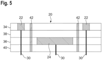
- Figure 5 shows a cross section through a further exemplary embodiment of the RIS 20, wherein the RIS 20 comprises several layers.
- the RIS 20 may be established as a printed circuit board comprising several layers, wherein the antenna elements 22, 24 are embedded in the printed circuit board.
- the first antenna elements 22 are provided in a first layer 34, and the second antenna elements 22 are provided in a second layer 36 of the RIS 20.
- an intermediate layer 38 may be provided, particularly wherein the intermediate layer 38 may be attached to the first layer 34 and to the second layer 36 by means of an adhesive layer, respectively.
- the intermediate layer 38 may consist of any suitable electrically insulating material or combination of materials.
- a base layer 40 may be provided, wherein the second layer 36 may be attached to the base layer 40 via a further adhesive layer.
- the base layer 40 may consist of any suitable electrically insulating material or combination of materials.
- control connections 30 may extend from a bottom side of the RIS 20, particularly from a bottom side of the base layer 40, through the RIS 20 to the respective antenna element 22, 24.
- the RIS 20 may comprise shielding members 42 that are provided between the first antenna elements 22 and/or between the second antenna elements 24.
- the shielding members 42 are configured to shield the antenna elements 22, 24 from each other, such that electromagnetic waves are prevented from propagating between the antenna elements 22, 24.
- the shielding members 42 may be established as metal walls, respectively.
- the shielding members 42 may be established as via fences, respectively.
- shielding members 42 are established as metal walls, while the remaining shielding members 42 are established as via fences.
- circuitry e.g., one or more circuits
- circuitry operably couple two or more components, generate information, process information, analyze information, generate signals, encode/decode signals, convert signals, transmit and/or receive signals, control other devices, etc.
- Circuitry of any type can be used.
- circuitry includes, among other things, one or more computing devices such as a processor (e.g., a microprocessor), a central processing unit (CPU), a digital signal processor (DSP), an application-specific integrated circuit (ASIC), a field-programmable gate array (FPGA), a system on a chip (SoC), or the like, or any combinations thereof, and can include discrete digital or analog circuit elements or electronics, or combinations thereof.
- a processor e.g., a microprocessor
- CPU central processing unit
- DSP digital signal processor
- ASIC application-specific integrated circuit
- FPGA field-programmable gate array
- SoC system on a chip
- circuitry includes hardware circuit implementations (e.g., implementations in analog circuitry, implementations in digital circuitry, and the like, and combinations thereof).
- circuitry includes combinations of circuits and computer program products having software or firmware instructions stored on one or more computer readable memories that work together to cause a device to perform one or more protocols, methodologies or technologies described herein.
- circuitry includes circuits, such as, for example, microprocessors or portions of microprocessor, that require software, firmware, and the like for operation.
- circuitry includes one or more processors or portions thereof and accompanying software, firmware, hardware, and the like.
- the present application may reference quantities and numbers. Unless specifically stated, such quantities and numbers are not to be considered restrictive, but exemplary of the possible quantities or numbers associated with the present application. Also in this regard, the present application may use the term “plurality” to reference a quantity or number. In this regard, the term “plurality” is meant to be any number that is more than one, for example, two, three, four, five, etc. The terms “about”, “approximately”, “near” etc., mean plus or minus 5% of the stated value.
Landscapes
- Physics & Mathematics (AREA)
- Electromagnetism (AREA)
- Variable-Direction Aerials And Aerial Arrays (AREA)
Priority Applications (1)
| Application Number | Priority Date | Filing Date | Title |
|---|---|---|---|
| EP23154064.2A EP4407797A1 (de) | 2023-01-30 | 2023-01-30 | Rekonfigurierbare intelligente oberfläche und drahtloses kommunikationsnetzwerk |
Applications Claiming Priority (1)
| Application Number | Priority Date | Filing Date | Title |
|---|---|---|---|
| EP23154064.2A EP4407797A1 (de) | 2023-01-30 | 2023-01-30 | Rekonfigurierbare intelligente oberfläche und drahtloses kommunikationsnetzwerk |
Publications (1)
| Publication Number | Publication Date |
|---|---|
| EP4407797A1 true EP4407797A1 (de) | 2024-07-31 |
Family
ID=85150506
Family Applications (1)
| Application Number | Title | Priority Date | Filing Date |
|---|---|---|---|
| EP23154064.2A Pending EP4407797A1 (de) | 2023-01-30 | 2023-01-30 | Rekonfigurierbare intelligente oberfläche und drahtloses kommunikationsnetzwerk |
Country Status (1)
| Country | Link |
|---|---|
| EP (1) | EP4407797A1 (de) |
Citations (2)
| Publication number | Priority date | Publication date | Assignee | Title |
|---|---|---|---|---|
| US20170179596A1 (en) * | 2014-04-30 | 2017-06-22 | Agence Spatiale Européenne | Wideband reflectarray antenna for dual polarization applications |
| CN108110428A (zh) * | 2017-11-29 | 2018-06-01 | 上海无线电设备研究所 | 一种适用于电磁开关的有源频率选择表面 |
-
2023
- 2023-01-30 EP EP23154064.2A patent/EP4407797A1/de active Pending
Patent Citations (2)
| Publication number | Priority date | Publication date | Assignee | Title |
|---|---|---|---|---|
| US20170179596A1 (en) * | 2014-04-30 | 2017-06-22 | Agence Spatiale Européenne | Wideband reflectarray antenna for dual polarization applications |
| CN108110428A (zh) * | 2017-11-29 | 2018-06-01 | 上海无线电设备研究所 | 一种适用于电磁开关的有源频率选择表面 |
Non-Patent Citations (2)
| Title |
|---|
| CHEN XIANGYU ET AL: "Design and Implementation of MIMO Transmission Based on Dual-Polarized Reconfigurable Intelligent Surface", IEEE WIRELESS COMMUNICATIONS LETTERS, IEEE, PISCATAWAY, NJ, USA, vol. 10, no. 10, 6 July 2021 (2021-07-06), pages 2155 - 2159, XP011881671, ISSN: 2162-2337, [retrieved on 20211005], DOI: 10.1109/LWC.2021.3095172 * |
| MENER SIMON ET AL: "Dual Circularly Polarized Reflectarray With Independent Control of Polarizations", IEEE TRANSACTIONS ON ANTENNAS AND PROPAGATION, IEEE, USA, vol. 63, no. 4, 30 January 2015 (2015-01-30), pages 1877 - 1881, XP011577997, ISSN: 0018-926X, [retrieved on 20150406], DOI: 10.1109/TAP.2015.2398458 * |
Similar Documents
| Publication | Publication Date | Title |
|---|---|---|
| US11482787B2 (en) | Antenna and antenna module including the antenna | |
| US12218434B2 (en) | Stack patch antenna assembly | |
| US9548544B2 (en) | Antenna element for signals with three polarizations | |
| US6424313B1 (en) | Three dimensional packaging architecture for phased array antenna elements | |
| US8723748B2 (en) | Dual frequency antenna aperture | |
| KR102276509B1 (ko) | 안테나 및 이를 구비하는 안테나 모듈 | |
| US20170222333A1 (en) | Wireless communication module | |
| KR102020676B1 (ko) | 안테나 모듈 | |
| WO2007103589A2 (en) | Multi-beam tile array module for phased array systems | |
| KR102549921B1 (ko) | 칩 안테나 모듈 | |
| WO2012162692A2 (en) | High impedance surface | |
| EP2763239B1 (de) | Funkfrequenzerdungsfolie für eine phasengesteuerte Gruppenantenne | |
| KR102382241B1 (ko) | 칩 안테나 및 이를 포함하는 칩 안테나 모듈 | |
| US9653807B2 (en) | Planar array antenna having antenna elements arranged in a plurality of planes | |
| WO2009150609A1 (en) | Micro-strip planar array antenna for satellite telecommunications, adapted to operate at different reception and transmission frequencies and with cross-polarizations | |
| US20250357664A1 (en) | Antenna apparatus and in-line calibration system for same | |
| US20030227420A1 (en) | Integrated aperture and calibration feed for adaptive beamforming systems | |
| CN112072326B (zh) | 用于通信的装置、便携式电子设备、以及网络设备 | |
| JP2001177338A (ja) | 移動体識別装置および移動体識別システム | |
| JP7591401B2 (ja) | アレイアンテナ | |
| CN111684656A (zh) | 用于与应答器通信的天线 | |
| KR101191819B1 (ko) | 반사판 및 리플렉트어레이 안테나 | |
| KR102054237B1 (ko) | 칩 안테나 및 이를 포함하는 칩 안테나 모듈 | |
| RU2279742C2 (ru) | Фазированная антенная решетка двойной поляризации | |
| JP2017184150A (ja) | アンテナ装置 |
Legal Events
| Date | Code | Title | Description |
|---|---|---|---|
| PUAI | Public reference made under article 153(3) epc to a published international application that has entered the european phase |
Free format text: ORIGINAL CODE: 0009012 |
|
| STAA | Information on the status of an ep patent application or granted ep patent |
Free format text: STATUS: THE APPLICATION HAS BEEN PUBLISHED |
|
| AK | Designated contracting states |
Kind code of ref document: A1 Designated state(s): AL AT BE BG CH CY CZ DE DK EE ES FI FR GB GR HR HU IE IS IT LI LT LU LV MC ME MK MT NL NO PL PT RO RS SE SI SK SM TR |
|
| STAA | Information on the status of an ep patent application or granted ep patent |
Free format text: STATUS: REQUEST FOR EXAMINATION WAS MADE |
|
| 17P | Request for examination filed |
Effective date: 20250120 |