EP4407659A1 - Base material which is used for adhesive sheet for processing semiconductor wafer having projected part - Google Patents
Base material which is used for adhesive sheet for processing semiconductor wafer having projected part Download PDFInfo
- Publication number
- EP4407659A1 EP4407659A1 EP22883392.7A EP22883392A EP4407659A1 EP 4407659 A1 EP4407659 A1 EP 4407659A1 EP 22883392 A EP22883392 A EP 22883392A EP 4407659 A1 EP4407659 A1 EP 4407659A1
- Authority
- EP
- European Patent Office
- Prior art keywords
- base material
- semiconductor wafer
- adhesive sheet
- adhesive
- layer
- Prior art date
- Legal status (The legal status is an assumption and is not a legal conclusion. Google has not performed a legal analysis and makes no representation as to the accuracy of the status listed.)
- Withdrawn
Links
Images

Classifications
-
- H—ELECTRICITY
- H10—SEMICONDUCTOR DEVICES; ELECTRIC SOLID-STATE DEVICES NOT OTHERWISE PROVIDED FOR
- H10P—GENERIC PROCESSES OR APPARATUS FOR THE MANUFACTURE OR TREATMENT OF DEVICES COVERED BY CLASS H10
- H10P72/00—Handling or holding of wafers, substrates or devices during manufacture or treatment thereof
- H10P72/70—Handling or holding of wafers, substrates or devices during manufacture or treatment thereof for supporting or gripping
-
- C—CHEMISTRY; METALLURGY
- C09—DYES; PAINTS; POLISHES; NATURAL RESINS; ADHESIVES; COMPOSITIONS NOT OTHERWISE PROVIDED FOR; APPLICATIONS OF MATERIALS NOT OTHERWISE PROVIDED FOR
- C09J—ADHESIVES; NON-MECHANICAL ASPECTS OF ADHESIVE PROCESSES IN GENERAL; ADHESIVE PROCESSES NOT PROVIDED FOR ELSEWHERE; USE OF MATERIALS AS ADHESIVES
- C09J7/00—Adhesives in the form of films or foils
- C09J7/20—Adhesives in the form of films or foils characterised by their carriers
- C09J7/22—Plastics; Metallised plastics
-
- C—CHEMISTRY; METALLURGY
- C09—DYES; PAINTS; POLISHES; NATURAL RESINS; ADHESIVES; COMPOSITIONS NOT OTHERWISE PROVIDED FOR; APPLICATIONS OF MATERIALS NOT OTHERWISE PROVIDED FOR
- C09J—ADHESIVES; NON-MECHANICAL ASPECTS OF ADHESIVE PROCESSES IN GENERAL; ADHESIVE PROCESSES NOT PROVIDED FOR ELSEWHERE; USE OF MATERIALS AS ADHESIVES
- C09J7/00—Adhesives in the form of films or foils
- C09J7/20—Adhesives in the form of films or foils characterised by their carriers
- C09J7/29—Laminated material
-
- H—ELECTRICITY
- H10—SEMICONDUCTOR DEVICES; ELECTRIC SOLID-STATE DEVICES NOT OTHERWISE PROVIDED FOR
- H10P—GENERIC PROCESSES OR APPARATUS FOR THE MANUFACTURE OR TREATMENT OF DEVICES COVERED BY CLASS H10
- H10P54/00—Cutting or separating of wafers, substrates or parts of devices
-
- C—CHEMISTRY; METALLURGY
- C09—DYES; PAINTS; POLISHES; NATURAL RESINS; ADHESIVES; COMPOSITIONS NOT OTHERWISE PROVIDED FOR; APPLICATIONS OF MATERIALS NOT OTHERWISE PROVIDED FOR
- C09J—ADHESIVES; NON-MECHANICAL ASPECTS OF ADHESIVE PROCESSES IN GENERAL; ADHESIVE PROCESSES NOT PROVIDED FOR ELSEWHERE; USE OF MATERIALS AS ADHESIVES
- C09J2203/00—Applications of adhesives in processes or use of adhesives in the form of films or foils
- C09J2203/326—Applications of adhesives in processes or use of adhesives in the form of films or foils for bonding electronic components such as wafers, chips or semiconductors
-
- C—CHEMISTRY; METALLURGY
- C09—DYES; PAINTS; POLISHES; NATURAL RESINS; ADHESIVES; COMPOSITIONS NOT OTHERWISE PROVIDED FOR; APPLICATIONS OF MATERIALS NOT OTHERWISE PROVIDED FOR
- C09J—ADHESIVES; NON-MECHANICAL ASPECTS OF ADHESIVE PROCESSES IN GENERAL; ADHESIVE PROCESSES NOT PROVIDED FOR ELSEWHERE; USE OF MATERIALS AS ADHESIVES
- C09J2301/00—Additional features of adhesives in the form of films or foils
- C09J2301/30—Additional features of adhesives in the form of films or foils characterized by the chemical, physicochemical or physical properties of the adhesive or the carrier
- C09J2301/312—Additional features of adhesives in the form of films or foils characterized by the chemical, physicochemical or physical properties of the adhesive or the carrier parameters being the characterizing feature
-
- C—CHEMISTRY; METALLURGY
- C09—DYES; PAINTS; POLISHES; NATURAL RESINS; ADHESIVES; COMPOSITIONS NOT OTHERWISE PROVIDED FOR; APPLICATIONS OF MATERIALS NOT OTHERWISE PROVIDED FOR
- C09J—ADHESIVES; NON-MECHANICAL ASPECTS OF ADHESIVE PROCESSES IN GENERAL; ADHESIVE PROCESSES NOT PROVIDED FOR ELSEWHERE; USE OF MATERIALS AS ADHESIVES
- C09J2467/00—Presence of polyester
- C09J2467/006—Presence of polyester in the substrate
-
- C—CHEMISTRY; METALLURGY
- C09—DYES; PAINTS; POLISHES; NATURAL RESINS; ADHESIVES; COMPOSITIONS NOT OTHERWISE PROVIDED FOR; APPLICATIONS OF MATERIALS NOT OTHERWISE PROVIDED FOR
- C09J—ADHESIVES; NON-MECHANICAL ASPECTS OF ADHESIVE PROCESSES IN GENERAL; ADHESIVE PROCESSES NOT PROVIDED FOR ELSEWHERE; USE OF MATERIALS AS ADHESIVES
- C09J2477/00—Presence of polyamide
- C09J2477/006—Presence of polyamide in the substrate
-
- C—CHEMISTRY; METALLURGY
- C09—DYES; PAINTS; POLISHES; NATURAL RESINS; ADHESIVES; COMPOSITIONS NOT OTHERWISE PROVIDED FOR; APPLICATIONS OF MATERIALS NOT OTHERWISE PROVIDED FOR
- C09J—ADHESIVES; NON-MECHANICAL ASPECTS OF ADHESIVE PROCESSES IN GENERAL; ADHESIVE PROCESSES NOT PROVIDED FOR ELSEWHERE; USE OF MATERIALS AS ADHESIVES
- C09J2479/00—Presence of polyamine or polyimide
- C09J2479/08—Presence of polyamine or polyimide polyimide
- C09J2479/086—Presence of polyamine or polyimide polyimide in the substrate
-
- H—ELECTRICITY
- H10—SEMICONDUCTOR DEVICES; ELECTRIC SOLID-STATE DEVICES NOT OTHERWISE PROVIDED FOR
- H10P—GENERIC PROCESSES OR APPARATUS FOR THE MANUFACTURE OR TREATMENT OF DEVICES COVERED BY CLASS H10
- H10P72/00—Handling or holding of wafers, substrates or devices during manufacture or treatment thereof
- H10P72/70—Handling or holding of wafers, substrates or devices during manufacture or treatment thereof for supporting or gripping
- H10P72/74—Handling or holding of wafers, substrates or devices during manufacture or treatment thereof for supporting or gripping using temporarily an auxiliary support
- H10P72/7402—Wafer tapes, e.g. grinding or dicing support tapes
-
- H—ELECTRICITY
- H10—SEMICONDUCTOR DEVICES; ELECTRIC SOLID-STATE DEVICES NOT OTHERWISE PROVIDED FOR
- H10P—GENERIC PROCESSES OR APPARATUS FOR THE MANUFACTURE OR TREATMENT OF DEVICES COVERED BY CLASS H10
- H10P72/00—Handling or holding of wafers, substrates or devices during manufacture or treatment thereof
- H10P72/70—Handling or holding of wafers, substrates or devices during manufacture or treatment thereof for supporting or gripping
- H10P72/74—Handling or holding of wafers, substrates or devices during manufacture or treatment thereof for supporting or gripping using temporarily an auxiliary support
- H10P72/7416—Handling or holding of wafers, substrates or devices during manufacture or treatment thereof for supporting or gripping using temporarily an auxiliary support used during dicing or grinding
Definitions
- This invention relates to a base material used for adhesive sheets for processing semiconductor wafers, which are used for grinding and cutting the backside of the semiconductor wafers.
- Adhesive sheets are required to have adhesion to pattern surfaces with unevenness such as protruding electrodes (bumps) and an ability to follow the unevenness of the pattern surfaces (step-following property), from the standpoint of reliability in protecting the pattern surfaces.
- Patent Document 1 discloses that the base material film as the adhesive tape is made of a base material film with excellent heat resistance to prevent stage adsorption failure even when applied to high-vacuum and high-temperature processes.
- Patent Document 1 JP2020-155688A
- the present invention was made in view of these circumstances, and provides a base material for processing a semiconductor wafer, which can improve the adhesion of the base material to the stage in the step of processing the semiconductor wafer.
- the inventors have studied the above problems and found that the problems can be solved when each thermal shrinkage of the base material in MD and TD after heating at 130°C for 10 minutes is 0% or higher, and thus the invention has been completed.
- a base material used for an adhesive sheet for processing a semiconductor wafer having projected portions in which each thermal shrinkage of the base material in MD and TD after heating at 130°C for 10 minutes is 0% or higher.
- a ratio of the thermal shrinkages of the base material in MD and TD (MD/TD) after heating at 130°C for 10 minutes is 3.5 or less.
- each thermal shrinkage of the base material in MD and TD after heating at 130°C for 10 minutes is 1.0% or less.
- the base material has a support layer and a cushion layer.
- the cushion layer has a melting point of 70°C or higher.
- an adhesive sheet for processing a semiconductor wafer having projected portions including the base material and an adhesive layer provided on the base material, in which the adhesive sheet is configured so that the projected portions are protected by the base material when the semiconductor wafer is attached to the adhesive layer.
- the support layer is provided on the opposite side of the adhesive layer as viewed from the cushion layer.
- the projected portions are protected by being embedded in the base material.
- the semiconductor wafer is attached to the adhesive layer.
- the dicing step further includes a fixing step, in which in the fixing step, the semiconductor wafer is fixed to a table via the adhesive sheet.
- an adhesive sheet for processing a semiconductor wafer that does not cause sagging in the base material during heating and attaching with the ring frame and semiconductor wafer, and that has improved adhesion to a stage set in equipment during dicing and backgrinding.
- Figs. 1 to 4E describe a base material 1 and an adhesive sheet 10 of an embodiment of the present invention.
- the adhesive sheet 10 of this embodiment has the base material 1 and an adhesive layer 2 provided on the base material 1.
- the adhesive sheet 10 is used for grinding a back surface 4b of a semiconductor wafer 4 having projected portions 5 and for dicing the semiconductor wafer 4. Each configuration is described below.
- the base material 1 may have an oxygen permeability of 1000 ml/(m 2 ⁇ 24h ⁇ atm) or less as measured according to JIS K 7126-2 (isobaric method) at 25°C and under RH 0%.
- each thermal shrinkage of the base material 1 in MD and TD after heating at 130°C for 10 minutes may be 0% or higher, and it is preferable that the thermal shrinkage after heating at 80 to 150°C for 10 minutes is 0% or higher, for example.
- Each thermal shrinkage is calculated from the respective formulae below by measuring the MD and TD lengths of the base material 1 with 100 mm on each side after placing it in an oven at 130°C for 10 minutes and then under atmosphere at 23°C for 2 hours.
- MD thermal shrinkage [(100 mm - length of MD after heating) / 100 mm] * 100
- TD thermal shrinkage 100 mm ⁇ length of TD after heating / 100 mm * 100
- the ratio of thermal shrinkages of the base material 1 in MD and TD (MD/TD) after heating at 130°C for 10 minutes may be 0 to 3.5 (e.g., 3.5, 3.4, 3.3, 3.2, 3.1, 3.0, 2.9, 2.8, 2.7, 2.6, 2.5, 2.4, 2.3, 2.2, 2.1, 2.0, 1.9, 1.8, 1.7, 1.6, 1.5, 1.4, 1.3, 1.2, 1.1, 1.0, 0.9, 0.8, 0.7, 0.6, 0.5, 0.4, 0.3, 0.2, 0.1, 0.05 and 0.01 or less).
- the ratio of thermal shrinkage is 0 to 3.5, the adhesion is improved.
- Each thermal shrinkage of the base material 1 in MD and TD after heating at 130° C for 10 minutes may be 1.0% or less (e.g., 1.0, 0.9, 0.8, 0.7, 0.6, 0.5, 0.4, 0.3, 0.2, 0.1, 0.05, and 0.01). If each of MD thermal shrinkage and TD thermal shrinkage is 1.0% or less, the ring frame and semiconductor wafer are not subjected to too much shrinkage stress during heating and attaching with the ring frame and semiconductor wafer, thereby reducing peeling from the ring frame, and cracking and chipping of the semiconductor wafer during back grinding and dicing.
- the base material 1 shown in Fig. 1 has a support layer 1b and a cushion layer 1a.
- the support layer 1b may be attached to the cushion layer 1a via an adhesive layer not shown.
- the thickness of the entire base material 1 is preferably from 50 to 400 ⁇ m, more preferably from 100 to 350 ⁇ m, and even more preferably from 150 to 300 ⁇ m. This thickness is specifically 50, 100, 150, 200, 250, 300, 350 or 400 ⁇ m, for example, and may be in the range between any two of the values exemplified above.
- MD and TD of the base material 1 can be adjusted by thermal history of the base material 1 (in particular, the support layer 1b) during its manufacture.
- the thermal history can be determined by differential scanning calorimetry.
- the thermal history may be strength of the base material 1 pulled in MD and TD by biaxial stretching during the manufacture of the base material 1.
- each thermal shrinkage of the base material 1 in MD and TD after heating at a temperature of 130°C or less for 10 minutes can be 0% or higher.
- the base material 1 has not undergone any treatment (e.g., annealing) after its manufacture that changes or eliminates the thermal history.
- the cushion layer 1a has a melting point of 70°C or higher, preferably 80°C or higher, and more preferably 85°C or higher.
- the upper limit of the melting point of the cushion layer 1a of the layers to be laminated is not particularly limited, but is preferably 200°C or less, and more preferably 150°C or less.
- the melting point is 70°C or higher, the opposite side laminated with the base material film does not have adhesive properties, and blocking can be reduced when the base material film is rolled up.
- the melting point of the cushion layer 1a can be measured in accordance with JIS K7121.
- the cushion layer 1a with the melting point of 70° C or higher is provided with the adhesive layer 2 on a part or the entire surface opposite to the side on which the above base material film is laminated. If the adhesive layer 2 is not partially or entirely provided, a portion without the adhesive layer 2 may peel off from the ring frame 3 during heating and attaching with the ring frame 3.
- a resin for the cushion layer 1a may contain additives as needed.
- the cushion layer 1a may be used alone or in combination of two or more types.
- the resin for the cushion layer 1a with the melting point of 70°C or higher is not limited, but includes, for example, ionomer resin, ethylene-vinyl acetate copolymer, soft polypropylene resin, ethylene-(meth)acrylic acid copolymer resin, styrene-butadiene copolymer resin, hydrogenated styrene-butadiene copolymer resin, ethylene-1-butene copolymer resin, and soft acrylic resin.
- the resin may be used alone or in combination with two or more types.
- the ionomer resin is not limited as long as a predetermined polymer is intermolecularly bonded with metal ions, but includes, for example, polyolefin ionomers, acrylic ionomers, polystyrene ionomers, and polyester ionomers. These ionomer resins may be used alone or in combination. Among these, polyolefin-based ionomers and acrylic-based ionomers are preferred, and polyolefin-based ionomers are more preferred. The use of such resins tends to improve the tracking and peeling properties.
- the polyolef-based ionomers are not limited, but include, for example, ethylene-methacrylate copolymers, ethylene-acrylate copolymers, ethylene- methacrylate-acrylate copolymers, and the like.
- the acrylic-based ionomers are not limited, but include, for example, acrylic ester-acrylate copolymers, acrylic ester-methacrylate copolymers, methacrylic ester-acrylate copolymers, methacrylic ester-methacrylate copolymers and the like.
- the polystyrene-based ionomers are not limited, but include, for example, styrene-styrenesulfonate copolymers, styrene-acrylate copolymers, styrene-methacrylate copolymers, styrene-styrene carboxylate copolymer, styrene-N-methyl 4-vinylpyridinium salt copolymer and the like.
- polyester-based ionomers are not limited, but include, for examples, sulfoterephthalate copolymerized polyethylene terephthalate, sulfoisophthalate copolymerized polyethylene terephthalate, sulfoterephthalate copolymerized polybutylene terephthalate, sulfoisophthalate copolymerized polybutylene terephthalate and the like.
- the metal ions constituting the salts of the above ionomer resins are not limited, but include, for example, monovalent metal ions such as sodium and lithium ions; divalent metal ions such as zinc, calcium, and magnesium ions; trivalent metal ions such as aluminum ions; and the like.
- the polymer and metal ions in the ionomer resin can be used in any combination based on the ionic functional group in the polymer and the valence of the metal ion.
- the ethylene-vinyl acetate copolymer is not limited as long as it is a copolymer of ethylene and vinyl acetate.
- the content of vinyl acetate in the ethylene-vinyl acetate copolymer is preferably 1 to 35 mol%, more preferably 3 to 25 mol%, and even more preferably 3 to 15 mol%, relative to the total number of moles of the component units derived from ethylene and vinyl acetate.
- the content of vinyl acetate is within the above range, the tracking and peeling properties tend to be more improved.
- the soft polypropylene resins are not limited, but include, for example, rubber components or polyolefin resins blended with polypropylene resins and propylene-or olefin random copolymers.
- the rubber components used here are not limited, but include, for example, styrene-butadiene copolymerized rubber, hydrogenated styrene-butadiene copolymerized rubber, styrene-butadiene-styrene block copolymerized rubber, hydrogenated styrene-butadiene-styrene block copolymerized rubber, styrene-isoprene-styrene block copolymerized rubber, ethylene-propylene copolymerized rubber and the liek.
- the polyolefin resins used here include polyethylene resin, polypropylene resin, and cyclo-olefin polymer resin, preferably, polyethylene resin.
- the ⁇ -olefins of copolymerization components used here include ethylene, 1-butene, 1-pentene, 1-hexene, 4-methyl-1-pentene, 1-heptene, 1-octene and the like.
- propylene- ⁇ -olefin random copolymers are propylene-ethylene random copolymer, propylene-1-butene random copolymer, and propylene-1-hexene random copolymer, propylene ethylene-1-butene copolymer, and the like, preferably propylene-ethylene random copolymer.
- the mass average molecular weight (Mw) of the resin of the cushion layer 1a which has a melting point of 70° C or higher, is preferably 10,000 to 1,000,000, more preferably 50,000 to 500,000.
- the mass average molecular weight (Mw) is a polystyrene equivalent value measured by gel permeation chromatography (GPC) under the measurement conditions described below.
- Equipment name SYSTEM-21 Shodex (manufactured by Showa Denko) Column: 3 PL gel MIXED-Bs in series Temperature: 40°C Detection: Differential refractive index Solvent: Tetrahydrofuran Concentration: 2 mass percent
- Calibration curve Standard polystyrene (PS) (manufactured by PL) was used to prepare the calibration curve.
- the thickness of the cushion layer 1a with the melting point of 70°C or higher is preferably 50 to 500 ⁇ m, more preferably 70 to 400 ⁇ m, and even more preferably 100 to 300 ⁇ m.
- the thickness of the cushion layer 1a with the melting point of 70°C or higher is within the above range to provide sufficient tracking and adhesiveness against unevenness caused by scratches on the surface of the ring frame and unevenness on the surface of the semiconductor wafer.
- the cushion layer 1a with the melting point of 70°C or higher can be produced in accordance with well-known techniques.
- the forming method is not particularly limited, but the above various materials are mixed so that each component is uniformly dispersed using customary melt-kneading and various mixing devices (single- or twinscrew extruders, rolls, Banbury mixers, various kneaders, etc.), the mixture is formed into a film using the T-die method, calendering method, or inflation method, and then laminated with the support layer 1b via an adhesive.
- the resin of cushion layer 1a with the melting point of 70°C or higher may contain other additives such as known plasticizers, heat stabilizers, colorants, organic or inorganic lubricants, surfactants, processing aids and the linke, as needed.
- the support layer 1b is a layer to maintain flatness of the wafer after grinding. Without the support layer, the backside of the base material would be uneven due to the projected portions 5 of the wafer, resulting in poor backside grindability.
- the adhesive sheet 10 can be attached to the semiconductor wafer 4 under normal or reduced pressure.
- the support layer 1b have preferably gas barrier properties.
- the support layer 1b has low oxygen permeability, it usually also has low air permeability, so the support layer 1b prevents outside air from entering a sealed space 2b through the base material 1, thereby making it easier for the base material 1 to follow the projected portions 5.
- the support layer 1b is provided so that the oxygen permeability of the base material 1 measured according to JIS K 7126-2 (isobaric method) at 25°C and under RH 0% is 1000 ml / (m 2 ⁇ 24h ⁇ atm) or less.
- the oxygen permeability of the support layer 1b alone under the same conditions is 1000 ml / (m 2 ⁇ 24h ⁇ atm) or less in order to ensure that the oxygen permeability of the base material 1 falls within such a range. In such a case, the above effect is easily exerted.
- the oxygen permeability of the base material 1 or the support layer 1b is, for example, 0 to 1000 ml / (m 2 ⁇ 24h ⁇ atm), and preferably 0 to 500 ml / (m 2 ⁇ 24h ⁇ atm), specifically, may be 0, 100, 200, 300, 400, 500, 600, 700, 800, 900 or 1000 ml / (m 2 ⁇ 24h ⁇ atm), or may be in the range between any two of the values examplified above.
- the oxygen permeability of the support layer 1b under the above conditions is lower than that of the cushion layer 1a.
- the value of (oxygen permeability of cushion layer 1a - oxygen permeability of support layer 1b) is 100 ml / (m 2 ⁇ 24h ⁇ atm) or higher. This value is, for example, 100 to 3000 ml / (m 2 ⁇ 24h ⁇ atm), specifically may be 100, 500, 1000,1500, 2000, 2500, 3000 ml / (m 2 ⁇ 24h ⁇ atm), or may be in the range between any two of the values examplified above.
- Polyester e.g., polyethylene terephthalate (PET)
- PET polyethylene terephthalate
- polyimide polyimide
- polyamide e.g., nylon
- the thickness of the support layer 1b is, for example, 5 to 50 ⁇ m, preferably 10 to 30 ⁇ m. If the support layer 1b is too thin, the flatness of the wafer after grinding is low. If the support layer 1b is too thick, the base material 1 may not follow the projected portions 5 of the base material 1. This thickness is specifically 5, 10, 11, 12, 13, 14, 15, 20, 21, 23, 24, 25, 30, 35, 40, 45, or 50 ⁇ m, for example, or may be in the range between any two of the values examplified above.
- Young's modulus of the support layer 1b is 500 MPa to 5000 MPa, preferably 1000 MPa to 4500 MPa.
- the Young's modulus in this embodiment can be measured at a pulling speed of 300 mm/min at a temperature of 23 ⁇ 2°C and under a humidity of 50 ⁇ 5%.
- the adhesive layer 2 is a layer for attaching the adhesive sheet 10 to the semiconductor wafer 4, and is formed by an adhesive.
- the shape of the adhesive layer 2 is not limited as long as it is a shape that enables the adhesive sheet 10 to be attached to the semiconductor wafer 4.
- the adhesive layer 2 may be configured with an aperture smaller in diameter than the diameter of the semiconductor wafer 4.
- the aperture is a portion where no adhesive is provided and is smaller in diameter than the diameter of the semiconductor wafer 4.
- the diameter of the aperture / the diameter of the semiconductor wafer 4 is preferably 0.950 to 0.995, and more preferably 0.960 to 0.990.
- a peripheral portion 4a of the semiconductor wafer 4 is attached to the adhesive layer 2 so that the projected portions 5 of the semiconductor wafer 4 are placed within the aperture. Therefore, the projected portions 5 do not come into contact with the adhesive, and the adhesive is prevented from remaining on the projected portions 5.
- the thickness of the adhesive layer 2 is usually from 1 to 200 ⁇ m, preferably from 2 to 170 ⁇ m, and more preferably from 5 to 150 ⁇ m. If the thickness of the adhesive layer 2 is less than 1 ⁇ m, sufficient adhesive strength to the surface of the ring frame 3 or the surface of the semiconductor wafer 4 cannot be ensured. If the thickness of the adhesive layer 2 is thicker than 200 ⁇ m, the adhesive may remain on the surface of the ring frame 3 or the semiconductor wafer 4 when removing the adhesive sheet 10 from the surface of the ring frame 3 or the surface of the semiconductor wafer 4, which reduces economic efficiency.
- the adhesive in the adhesive layer 2 is not particularly limited, but may include, for example, a polymer and a curing agent, and may include other components as needed.
- the polymer included in the adhesive layer 2 is not particularly limited, but may include, for example, (meth)acrylic ester copolymers having a linear, branched, or cross-linked form.
- branches There are two types of branches possessed by the polymer with the branched form: short-chain branches, which are branches with a length of up to several carbons; and long-chain branches, which are branches with a length comparable to that of the main chain.
- the polymer in the cross-linked form may also have a three-dimensional network structure.
- the polymer in the cross-linked form also includes those formed by the reaction of the polymer and the curing agent described below.
- the constituent units of (meth)acrylic acid ester copolymers include alkyl group-containing constituent units, hydroxyl group-containing constituent units, carboxyl group-containing constituent units, and other constituent units. These constituent units are mainly derived from (meth)acrylic acid monomers or (meth)acrylic ester monomers, but (meth)acrylic ester copolymers are not limited to polymers composed solely of (meth)acrylic acid or its esters, and can also be derived from monomers having polymerizable double bonds other than (meth)acrylic acid, etc.
- (Meth)acrylic ester copolymers can be cross-linked with the curing agent described below due to the constituent units having hydroxyl groups and carboxyl groups. Such a crosslinked structure can improve the cohesive strength of the adhesive after adhesive application. Also, by adjusting the degree of cross-linking, the storage modulus and loss modulus, as well as 180°C peel strength and tack to the ring frame and semiconductor wafer can be adjusted.
- the constituent units having alkyl groups include monomers that do not have functional groups for crosslinking reactions with the curing agents described below.
- the monomers constituting the constituent units having such hydrocarbon groups are not limited, but include alkyl (meth)acrylates having linear, branched, or branched alkyl groups such as methyl groups, ethyl groups, n-pulpylic groups, isopulpylic groups, n-butyl groups, t-butyl groups, isobutyl groups, amyl groups, isoamyl groups, hexyl groups, heptyl groups, cyclohexyl groups, 2-ethylhexyl groups, octyl groups, isooctyl groups, nonyl groups, isononyl groups, decyl groups, isodecyl groups, undecyl groups, lauryl groups, tridecyl groups, tetradecyl groups, stearyl groups, oct
- the monomers constituting the constituent units having hydroxyl groups are not particularly limited, but include hydroxyl group-containing monomers such as 2-hydroxyethyl (meth)acrylate, 2-hydroxypropyl (meth)acrylate, 4-hydroxybutyl (meth)acrylate, 6-hydroxyhexyl (meth)acrylate, 8-hydroxyoctyl (meth)acrylate, 1-hydroxydecyl (meth)acrylate, 12-hydroxylauryl (meth)acrylate and (4-hydroxymethyl cyclohexyl) methyl (meth)acrylate. These may be used alone or in combination with two or more selected monomers.
- hydroxyl group-containing monomers such as 2-hydroxyethyl (meth)acrylate, 2-hydroxypropyl (meth)acrylate, 4-hydroxybutyl (meth)acrylate, 6-hydroxyhexyl (meth)acrylate, 8-hydroxyoctyl (meth)acrylate, 1-hydroxydecyl (meth)acrylate, 12-hydroxylauryl (me
- the monomers constituting the constituent units having carboxyl groups are not particularly limited, but include carboxyl group-containing monomers such as acrylic acid, methacrylic acid, carboxyethyl (meth)acrylate, carboxypentyl (meth)acrylate, itaconic acid, maleic acid, fumaric acid, and crotonic acid. These may be used alone or in combination with two or more selected monomers.
- the monomers constituting other constituent units other than the above are not particularly limited, but include, for example, acid anhydride monomers such as maleic anhydride and itaconic anhydride; sulfonic acid group-containing monomers such as styrene sulfonic acid, arylsulfonic acid, 2-(meth)acrylamido-2-methylpropanesulfonic acid, (meth)acrylamidopropanesulfonic acid, sulfopropyl (meth)acrylate, and (meth)acryloyloxynaphthalate; and phosphate group-containing monomers such as 2-hydroxyethylacryloylphosphate.
- acid anhydride monomers such as maleic anhydride and itaconic anhydride
- sulfonic acid group-containing monomers such as styrene sulfonic acid, arylsulfonic acid, 2-(meth)acrylamido-2-methylpropanesulfonic acid, (meth)
- the curing agents constituting the adhesive layer 2 are not particularly limited, but include isocyanate curing agents, epoxy curing agents, and amine curing agents, which may be single substances or mixtures. Among these, isocyanate compounds are preferred.
- Such isocyanate compounds are not particularly limited, but include, for example, aromatic isocyanates such as tolylene diisocyanate, 4, 4-diphenylmethane diisocyanate, xylylene diisocyanate, trimethylolpropane modified tolylene diisocyanate; alicyclic diisocyanates such as isophorone diisocyanate and methylenebis(4-cyclohexylisocyanate); aliphatic diisocyanates such as hexamethylene diisocyanate and trimethylhexamethylene diisocyanate. These may be used alone or in combination with two or more selected isocyanate compounds.
- aromatic isocyanates such as tolylene diisocyanate, 4, 4-diphenylmethane diisocyanate, xylylene diisocyanate, trimethylolpropane modified tolylene diisocyanate
- alicyclic diisocyanates such as isophorone diisocyanate and methylene
- surface treatment may be chemically or physically applied as necessary.
- the surface treatments include, for example, corona treatment, chromic acid treatment, ozone exposure, flame exposure, high voltage electric shock exposure, and ionizing radiation treatment.
- the adhesive layer 4 can be manufactured according to well-known techniques. Although the forming method is not particularly limited, the adhesive layer 2 is formed by dissolving the above various materials in a solvent such as an organic solvent to form a varnish, which is then coated on a protective film by a knife coat method, a roll coat method, a spray coat method, a gravure coat method, a bar coat method, a curtain coat method, a screen printing method or the like, and then removing the solvent.
- a solvent such as an organic solvent
- the semiconductor wafer 4 has the projected portions 5.
- Each of the projected portions 5 has any structure that protrudes in the out-of-plane direction of the semiconductor wafer 4.
- the projected portions 5 include, for example, protruding electrodes and projected portions of a circuit having concavoconvexities and convexities.
- the semiconductor wafer 4 includes not only a silicon wafer, but also a germanium wafer, a gallium-arsenide wafer, a gallium-phosphorus wafer, a gallium-arsenide- aluminum wafer, a sapphire wafer, a glass wafer, a silicon carbide wafe.
- the diameter of the semiconductor wafer 4 is preferably from 1 to 16 inches, more preferably 4 to 12 inches.
- the thickness of the semiconductor wafer 4 is not particularly limited, but preferably 500 to 800 ⁇ m, more preferably 520 to 775 ⁇ m.
- each of the projected portions 5 is preferably between 10 and 500 ⁇ m, more preferably between 100 and 300 ⁇ m. This height may specifically be, for example, 10, 50, 100, 150, 200, 250, 300, 350, 400, 450, or 500 ⁇ m, and may be in the range between any two of the values examplified above.
- the semiconductor wafer 4 may have the peripheral portion 4a without the projected portions 5.
- the width of the peripheral portion 4a is preferably 1.0 to 3.0 mm, more preferably 1.5 to 2.5 mm.
- End products using the semiconductor wafer 4 having the projected portions 5 include electronic components for logic, memory, sensors, power supplies, and other applications.
- This manufacturing method has a frame attaching step, a heating step, a grinding step, and a dicing step.
- the order in which these steps are carried out is not limited to this order, and the order can be interchanged as necessary. Each step is described below.
- the adhesive sheet 10 is attached to the ring frame 3.
- the ring frame 3 has an aperture 3a.
- the diameter of the aperture 3a is smaller than that of the adhesive layer 2. This allows the adhesive sheet 10 to be held stably in the ring frame 3, facilitating handling of the adhesive sheet 10.
- the adhesive sheet 10 is attached to the surface of the semiconductor wafer 4 having the projected portions 5 under normal or reduced pressure.
- This step can be performed by attaching the semiconductor wafer 4 to the adhesive sheet 10 in a vacuum chamber 16.
- the pressure in the vacuum chamber 16 need only be lower than atmospheric pressure, preferably at 1000 Pa or lower, more preferably at 500 Pa or lower, even more preferably at 100 Pa or lower.
- the lower limit of the pressure in the vacuum chamber 16 is not specified, but is, for example, 10 Pa.
- the base material 1 is pushed by the atmospheric pressure and enters the sealed space 2b.
- the base material 1 is rigid when not heated, and the base material 1 hardly enters the sealed space 2b.
- the base material 1 is heated to 60 to 150°C in the heating step, the base material 1 is softened and the sealed space 2b disappears or almost disappears, as shown in Fig. 2D .
- the ratio of the height of the embedded portion of the projected portion 5 / the height of the entire projected portion 5 is preferably 0.9 to 1, more preferably 0. 95 to 1, even preferably 0. 99 to 1.
- the heating temperature of the base material 1 is preferably 80 to 120°C.
- the heating time of the base material 1 is preferably from 3 to 120 seconds, and more preferably from 5 to 60 seconds.
- the heating of the base material 1 may be performed before or after attaching the semiconductor wafer 4 to the adhesive sheet 10.
- the heating may be performed in the vaccume chamber 16 or outside the vaccume chamber 16.
- the back surface 4b of the semiconductor wafer 4 is ground.
- the semiconductor wafer 4 is fixed to a suction table 6 via the adhesive sheet 10.
- the back surface 4b of the semiconductor wafer 4 is the opposite side of the surface on which the projected portions 5 are provided.
- the grinding is preferably performed while water is applied to the wafer and grinding wheel (e.g., diamond) to cool them.
- the thickness of the thinner wafer is preferably 300 ⁇ m or less, more preferably 150 ⁇ m or less.
- a curable resin may be used to prevent damage to the projected portions 5.
- the curable resin is a resin that hardens upon stimulation by energy rays (e.g., ultraviolet rays) or heat.
- the curable resin is preferably supported on a support film and placed between the support film and the support layer 1b of the adhesive sheet 10.
- the curable resin has preferably a viscosity of 100 to 3000 mPa ⁇ s, more preferably a viscosity of 100 to 3000 mPa ⁇ s before curing.
- the viscosity is 100 mPa ⁇ s or higher, the curable resin makes point contact instead of surface contact, resulting in excellent grindability.
- the viscosity is 3000 mPa ⁇ s or less, the curable resin does not easily entrap air bubbles when it flows between adjacent projected portions 5, resulting in excellent grindability.
- the viscosity is measured using an E-type viscometer at 23°C and 50 rpm.
- the curable resin has preferably Shore D hardness of 5 to 70, more preferably Shore D hardness of 10 to 60 after curing.
- Shore D hardness is 5 or higher, the projected portions 5 are retained well, resulting in excellent grindability.
- Shore D hardness is 70 or less, the adhesive sheet 10 can be easily curved when peeling the adhesive sheet 10 from the semiconductor wafer 4.
- the Shore D hardness is measured under conditions in accordance with JIS K 6253.
- the curable resin is preferably photo-curable resin, more preferably UV-curable resin.
- the curable resin is preferably based on acrylic resins, and their composition is not particularly limited, but the curable resin containing 1,2-hydrogenated polybutadiene-terminated urethane (meth)acrylate, isobornyl acrylate, or diethylacrylamide is preferred because it can improve the adhesion between the base material 1 and the support film 7.
- the cure shrinkage of the curable resin is preferably 7% or less.
- the thickness of the curable resin is preferably (Td + 20) to (Td + 200) ⁇ m, more preferably (Td + 50) to (Td + 150) ⁇ m.
- the support film is any film that can support the curable resin and can be made of polyolefins such as ethylene vinyl acetate, polyethylene, polypropylene, polybutene and polybutadiene; polyvinyl chloride; polyethylene terephthalate; polyethylene naphthalate; polystyrene; polycarbonate; polyimide; and the like.
- polyolefins such as ethylene vinyl acetate, polyethylene, polypropylene, polybutene and polybutadiene; polyvinyl chloride; polyethylene terephthalate; polyethylene naphthalate; polystyrene; polycarbonate; polyimide; and the like.
- the thickness of the support film is preferably 10 to 300 ⁇ m, more preferagly 30 to 250 ⁇ m.
- the semiconductor wafer is divided into individual pieces.
- the semiconductor wafer 4 is divided into multiple semiconductor chips by dicing on the ground semiconductor wafer 4.
- the dicing method is not limited and may be any method such as blade dicing, laser dicing, stealth dicing, plasma dicing, and the like.
- the dicing step may have a coating step in which a mask 8 capable of forming a pattern (groove) for the dicing by a patterning means (e.g., laser) is coated on the ground back surface 4b ( Fig. 4A ).
- the pattern for the dicing indicates the position where the dicing is to be performed.
- the mask 8 may be, for example, a (meth)acrylic copolymer.
- the ground semiconductor wafer 4 is fixed to a suction table 6' via the adhesive sheet 10.
- the dicing step may also include a pattern forming step in which a pattern 8a for the dicing is formed on the mask 8 by pattern forming means after the coating step ( Fig. 4B ).
- a pattern forming step By performing the dicing along the pattern 8a, the semiconductor wafer 4 can be easily divided into semiconductor chips having the desired size.
- the ground semiconductor wafer 4 is fixed to a suction table 6" via the adhesive sheet 10.
- Fig. 4C shows the dicing step in which the dicing is performed along the pattern 8a.
- the dicing step may further include a fixing step in which the semiconductor wafer 4 is fixed to a fixing table 7 (e.g., electrostatic table or suction table) via the adhesive sheet 10 before the dicing.
- a fixing table 7 e.g., electrostatic table or suction table
- the dicing step may have a dicing tape attaching step in which a dicing tape 9 is attached to the back surface 4b of the diced semiconductor wafer 4 ( Fig. 4D ).
- the dicing tape 9 may be attached to the back surface 4b of the semiconductor wafer 4 or may be attached to the back surface 4b of the semiconductor wafer 4 and the ring frame 3. This prevents one or more semiconductor chips from remaining attached to the adhesive sheet 10 during the peeling step ( Fig. 4E ) in which the adhesive sheet 10 is removed from the semiconductor wafer 4.
- the dicing tape 9 may be, for example, a UV curable dicing tape or a general pressure-sensitive dicing tape with low adhesive strength, and a substrate of the dicing tape may be polyolefin such as polyvinyl chloride, polyethylene and polypropylene.
- the semiconductor wafer 4 is fixed to the fixing table 6 (e.g., electrostatic table or suction table) via the adhesive sheet 10.
- the base material film was formed by dry lamination of polyethylene terephthalate film having a thickness of 25 ⁇ m (Toray, product number: Lumirror S10) and an ionomer film (melting point 82°C) having a thickness of 150 ⁇ m formed by the T-die method.
- the base material film was formed in the same way as in Example 1, except that the polyethylene terephthalate film was replaced with nylon film having a thickness of 15 ⁇ m (Toyobo, product number: N1202).
- the base material film was formed in the same way as in Example 1, except that the polyethylene terephthalate film was replaced with polyimide film having a thickness of 12 ⁇ m (SKC KOLON PI, product number: GF050).
- the base material film was formed in the same way as in Example 1, except that the polyethylene terephthalate film was replaced with a 12 iim thick polyethylene terephthalate film having a thickness of 12 ⁇ m (SHINKONG MATERIALS TECHNOLOGY, product number: P121).
- the base material film was formed in the same way as in Comparative Example 1, except that the polyethylene terephthalate film of Comparative Example 1 was annealed (at 200°C for 5 min).
- the base material film was formed in the same way as in Example 1, except that the polyethylene terephthalate film of Example 1 was annealed (at 200°C for 5 min).
- a silicon wafer is placed on a stage with the same diameter as that of the silicon wafer.
- the silicon wafer is heated at 130°C for 10 minutes with the base material layer bonded to the ring frame pressed on top of the silicon wafer.
- the entire silicon wafer is removed from the stage. After that, the base material layer is checked for sagging between the inner edge of the ring frame and the edge of the silicon wafer after 30 minutes of standing still under an atmosphere of 23°C.
- a silicon wafer is placed on a stage with the same diameter as that of the silicon wafer.
- the silicon wafer is heated at 130°C for 10 minutes with the base material layer attached to the ring frame pressed on top of the silicon wafer.
- the entire silicon wafer is removed from the stage. After that, the silicon wafer is placed under an atmosphere of 23°C for 30 minutes, and then the silicon wafer is checked for wrinkles on the surface where the base material layer is attached to the silicon wafer.
Landscapes
- Chemical & Material Sciences (AREA)
- Organic Chemistry (AREA)
- Container, Conveyance, Adherence, Positioning, Of Wafer (AREA)
- Mechanical Treatment Of Semiconductor (AREA)
- Laminated Bodies (AREA)
- Adhesive Tapes (AREA)
Abstract
Description
- This invention relates to a base material used for adhesive sheets for processing semiconductor wafers, which are used for grinding and cutting the backside of the semiconductor wafers.
- When processing semiconductor wafers, adhesive sheets are applied to protect them from damage. For example, during back grinding process when processing the semiconductor wafers, the adhesive sheet is attached to protect a pattern surface of the semiconductor wafer. Adhesive sheets are required to have adhesion to pattern surfaces with unevenness such as protruding electrodes (bumps) and an ability to follow the unevenness of the pattern surfaces (step-following property), from the standpoint of reliability in protecting the pattern surfaces.
-
Patent Document 1 discloses that the base material film as the adhesive tape is made of a base material film with excellent heat resistance to prevent stage adsorption failure even when applied to high-vacuum and high-temperature processes. - Patent Document 1:
JP2020-155688A - When the inventors made a diligent study of the adhesive sheet disclosed in
Patent Document 1, they found that the base material may not fully adhere to a stage due to the occurrence of sagging in the base material. Upon detailed investigation, it became clear that the conventional base material including the base material film disclosed inPatent Document 1 stretches unevenly in machine direction (MD) and/or transverse direction (TD) of the base material when heated, resulting in the occurrence of sagging in the base material. - The present invention was made in view of these circumstances, and provides a base material for processing a semiconductor wafer, which can improve the adhesion of the base material to the stage in the step of processing the semiconductor wafer.
- The inventors have studied the above problems and found that the problems can be solved when each thermal shrinkage of the base material in MD and TD after heating at 130°C for 10 minutes is 0% or higher, and thus the invention has been completed.
- According to the present invention, it is provided a base material used for an adhesive sheet for processing a semiconductor wafer having projected portions, in which each thermal shrinkage of the base material in MD and TD after heating at 130°C for 10 minutes is 0% or higher.
- Various embodiments of the invention are illustrated below. The embodiments shown below can be combined with each other.
- Preferably, a ratio of the thermal shrinkages of the base material in MD and TD (MD/TD) after heating at 130°C for 10 minutes is 3.5 or less.
- Preferably, each thermal shrinkage of the base material in MD and TD after heating at 130°C for 10 minutes is 1.0% or less.
- Preferably, the base material has a support layer and a cushion layer.
- Preferably, the cushion layer has a melting point of 70°C or higher.
- According to the present invention, it is also provided an adhesive sheet for processing a semiconductor wafer having projected portions, the adhesive sheet including the base material and an adhesive layer provided on the base material, in which the adhesive sheet is configured so that the projected portions are protected by the base material when the semiconductor wafer is attached to the adhesive layer.
- Preferably, the support layer is provided on the opposite side of the adhesive layer as viewed from the cushion layer.
- Preferably, the projected portions are protected by being embedded in the base material.
- Preferably, the semiconductor wafer is attached to the adhesive layer.
- According to the present invention, it is also provided a method for manufacturing semiconductor devices using the adhesive sheet,
- in which the method includes a frame attaching step, a wafer attaching step, a heating step, a grinding step, and a dicing step,
- in the frame attaching step, the adhesive sheet is attached to a ring frame,
- in the wafer attaching step, the adhesive sheet is attached to a surface with the projected portions of the semiconductor wafer,
- in the heating step, the base material is heated,
- in the grinding step, a back surface of the semiconductor wafer is ground, and
- in the dicing step, the semiconductor wafer is diced into individual pieces.
- Preferably, the dicing step further includes a fixing step, in which in the fixing step, the semiconductor wafer is fixed to a table via the adhesive sheet.
- According to the present invention, it is possible to provide an adhesive sheet for processing a semiconductor wafer that does not cause sagging in the base material during heating and attaching with the ring frame and semiconductor wafer, and that has improved adhesion to a stage set in equipment during dicing and backgrinding.
-
-
FIG. 1 shows a cross-sectional view of anadhesive sheet 10 equipped with abase material 1 according to an embodiment of the present invention; -
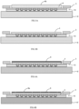
FIGs. 2A to 2D show cross-sectional views showing each step of a method for manufacturing a semiconductor device using theadhesive sheet 10 of the embodiment of the present invention; -
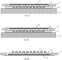
FIGs. 3A and 3B show cross-sectional views showing each step of the method for manufacturing the semiconductor device using theadhesive sheet 10 of the embodiment of the present invention; and -
FIGs. 4A to 4E show cross-sectional views showing each step of the method for manufacturing the semiconductor device using theadhesive sheet 10 of the embodiment of the present invention. - Embodiments of the invention are described below. The various features shown in the following embodiments can be combined with each other. In addition, each of the features can be independently inventive.
-
Figs. 1 to 4E describe abase material 1 and anadhesive sheet 10 of an embodiment of the present invention. Theadhesive sheet 10 of this embodiment has thebase material 1 and anadhesive layer 2 provided on thebase material 1. Theadhesive sheet 10 is used for grinding aback surface 4b of asemiconductor wafer 4 having projectedportions 5 and for dicing thesemiconductor wafer 4. Each configuration is described below. - The
base material 1 may have an oxygen permeability of 1000 ml/(m2·24h·atm) or less as measured according to JIS K 7126-2 (isobaric method) at 25°C and under RH 0%. In thebase material 1, each thermal shrinkage of thebase material 1 in MD and TD after heating at 130°C for 10 minutes may be 0% or higher, and it is preferable that the thermal shrinkage after heating at 80 to 150°C for 10 minutes is 0% or higher, for example. - Each thermal shrinkage is calculated from the respective formulae below by measuring the MD and TD lengths of the
base material 1 with 100 mm on each side after placing it in an oven at 130°C for 10 minutes and then under atmosphere at 23°C for 2 hours.MD thermal shrinkage = [(100 mm - length of MD after heating) / 100 mm] * 100 
- By using such the
base material 1 in which MD and TD thermal shrinkages after heating at 130°C for 10 minutes are 0% or higher, sagging of thebase material 1 can be suppressed during heating and attaching with a ring frame and a semiconductor wafer. This allows for improved adhesion to a stage set in the equipment for back grinding and dicing processes, resulting in contributing to yield improvement. If the thermal shrinkage of MD or TD is less than 0%, sagging occurs in thebase material 1 during heating and attaching with the ring frame and semiconductor wafer, resulting in poor adhesion to the stage set in the equipment for the back grinding and dicing processes. - The ratio of thermal shrinkages of the
base material 1 in MD and TD (MD/TD) after heating at 130°C for 10 minutes may be 0 to 3.5 (e.g., 3.5, 3.4, 3.3, 3.2, 3.1, 3.0, 2.9, 2.8, 2.7, 2.6, 2.5, 2.4, 2.3, 2.2, 2.1, 2.0, 1.9, 1.8, 1.7, 1.6, 1.5, 1.4, 1.3, 1.2, 1.1, 1.0, 0.9, 0.8, 0.7, 0.6, 0.5, 0.4, 0.3, 0.2, 0.1, 0.05 and 0.01 or less). When the ratio of thermal shrinkage is 0 to 3.5, the adhesion is improved. - Each thermal shrinkage of the
base material 1 in MD and TD after heating at 130° C for 10 minutes may be 1.0% or less (e.g., 1.0, 0.9, 0.8, 0.7, 0.6, 0.5, 0.4, 0.3, 0.2, 0.1, 0.05, and 0.01). If each of MD thermal shrinkage and TD thermal shrinkage is 1.0% or less, the ring frame and semiconductor wafer are not subjected to too much shrinkage stress during heating and attaching with the ring frame and semiconductor wafer, thereby reducing peeling from the ring frame, and cracking and chipping of the semiconductor wafer during back grinding and dicing. - The
base material 1 shown inFig. 1 has a support layer 1b and acushion layer 1a. The support layer 1b may be attached to thecushion layer 1a via an adhesive layer not shown. - The thickness of the
entire base material 1 is preferably from 50 to 400 µm, more preferably from 100 to 350 µm, and even more preferably from 150 to 300 µm. This thickness is specifically 50, 100, 150, 200, 250, 300, 350 or 400 µm, for example, and may be in the range between any two of the values exemplified above. - MD and TD of the
base material 1 can be adjusted by thermal history of the base material 1 (in particular, the support layer 1b) during its manufacture. The thermal history can be determined by differential scanning calorimetry. The thermal history may be strength of thebase material 1 pulled in MD and TD by biaxial stretching during the manufacture of thebase material 1. By manufacturing thebase material 1 so that the thermal history of MD ofbase material 1 is the same as that of TD of thebase material 1, each thermal shrinkage of thebase material 1 in MD and TD after heating at a temperature of 130°C or less for 10 minutes can be 0% or higher. Thebase material 1 has not undergone any treatment (e.g., annealing) after its manufacture that changes or eliminates the thermal history. - The
cushion layer 1a has a melting point of 70°C or higher, preferably 80°C or higher, and more preferably 85°C or higher. The upper limit of the melting point of thecushion layer 1a of the layers to be laminated is not particularly limited, but is preferably 200°C or less, and more preferably 150°C or less. When the melting point is 70°C or higher, the opposite side laminated with the base material film does not have adhesive properties, and blocking can be reduced when the base material film is rolled up. - The melting point of the
cushion layer 1a can be measured in accordance with JIS K7121. - The
cushion layer 1a with the melting point of 70° C or higher is provided with theadhesive layer 2 on a part or the entire surface opposite to the side on which the above base material film is laminated. If theadhesive layer 2 is not partially or entirely provided, a portion without theadhesive layer 2 may peel off from thering frame 3 during heating and attaching with thering frame 3. - A resin for the
cushion layer 1a may contain additives as needed. Thecushion layer 1a may be used alone or in combination of two or more types. - The resin for the
cushion layer 1a with the melting point of 70°C or higher is not limited, but includes, for example, ionomer resin, ethylene-vinyl acetate copolymer, soft polypropylene resin, ethylene-(meth)acrylic acid copolymer resin, styrene-butadiene copolymer resin, hydrogenated styrene-butadiene copolymer resin, ethylene-1-butene copolymer resin, and soft acrylic resin. The resin may be used alone or in combination with two or more types. - The ionomer resin is not limited as long as a predetermined polymer is intermolecularly bonded with metal ions, but includes, for example, polyolefin ionomers, acrylic ionomers, polystyrene ionomers, and polyester ionomers. These ionomer resins may be used alone or in combination. Among these, polyolefin-based ionomers and acrylic-based ionomers are preferred, and polyolefin-based ionomers are more preferred. The use of such resins tends to improve the tracking and peeling properties.
- The polyolef-based ionomers are not limited, but include, for example, ethylene-methacrylate copolymers, ethylene-acrylate copolymers, ethylene- methacrylate-acrylate copolymers, and the like.
- The acrylic-based ionomers are not limited, but include, for example, acrylic ester-acrylate copolymers, acrylic ester-methacrylate copolymers, methacrylic ester-acrylate copolymers, methacrylic ester-methacrylate copolymers and the like.
- The polystyrene-based ionomers are not limited, but include, for example, styrene-styrenesulfonate copolymers, styrene-acrylate copolymers, styrene-methacrylate copolymers, styrene-styrene carboxylate copolymer, styrene-N-methyl 4-vinylpyridinium salt copolymer and the like.
- The polyester-based ionomers are not limited, but include, for examples, sulfoterephthalate copolymerized polyethylene terephthalate, sulfoisophthalate copolymerized polyethylene terephthalate, sulfoterephthalate copolymerized polybutylene terephthalate, sulfoisophthalate copolymerized polybutylene terephthalate and the like.
- The metal ions constituting the salts of the above ionomer resins are not limited, but include, for example, monovalent metal ions such as sodium and lithium ions; divalent metal ions such as zinc, calcium, and magnesium ions; trivalent metal ions such as aluminum ions; and the like. The polymer and metal ions in the ionomer resin can be used in any combination based on the ionic functional group in the polymer and the valence of the metal ion.
- The ethylene-vinyl acetate copolymer is not limited as long as it is a copolymer of ethylene and vinyl acetate. The content of vinyl acetate in the ethylene-vinyl acetate copolymer is preferably 1 to 35 mol%, more preferably 3 to 25 mol%, and even more preferably 3 to 15 mol%, relative to the total number of moles of the component units derived from ethylene and vinyl acetate. When the content of vinyl acetate is within the above range, the tracking and peeling properties tend to be more improved.
- The soft polypropylene resins are not limited, but include, for example, rubber components or polyolefin resins blended with polypropylene resins and propylene-or olefin random copolymers. The rubber components used here are not limited, but include, for example, styrene-butadiene copolymerized rubber, hydrogenated styrene-butadiene copolymerized rubber, styrene-butadiene-styrene block copolymerized rubber, hydrogenated styrene-butadiene-styrene block copolymerized rubber, styrene-isoprene-styrene block copolymerized rubber, ethylene-propylene copolymerized rubber and the liek. The polyolefin resins used here include polyethylene resin, polypropylene resin, and cyclo-olefin polymer resin, preferably, polyethylene resin. The α-olefins of copolymerization components used here include ethylene, 1-butene, 1-pentene, 1-hexene, 4-methyl-1-pentene, 1-heptene, 1-octene and the like. Specific examples of propylene-α-olefin random copolymers are propylene-ethylene random copolymer, propylene-1-butene random copolymer, and propylene-1-hexene random copolymer, propylene ethylene-1-butene copolymer, and the like, preferably propylene-ethylene random copolymer.
- The mass average molecular weight (Mw) of the resin of the
cushion layer 1a, which has a melting point of 70° C or higher, is preferably 10,000 to 1,000,000, more preferably 50,000 to 500,000. - The mass average molecular weight (Mw) is a polystyrene equivalent value measured by gel permeation chromatography (GPC) under the measurement conditions described below.
Equipment name: SYSTEM-21 Shodex (manufactured by Showa Denko) Column: 3 PL gel MIXED-Bs in series Temperature: 40°C Detection: Differential refractive index Solvent: Tetrahydrofuran Concentration: 2 mass percent Calibration curve: Standard polystyrene (PS) (manufactured by PL) was used to prepare the calibration curve. - The thickness of the
cushion layer 1a with the melting point of 70°C or higher is preferably 50 to 500 µm, more preferably 70 to 400 µm, and even more preferably 100 to 300 µm. The thickness of thecushion layer 1a with the melting point of 70°C or higher is within the above range to provide sufficient tracking and adhesiveness against unevenness caused by scratches on the surface of the ring frame and unevenness on the surface of the semiconductor wafer. - The
cushion layer 1a with the melting point of 70°C or higher can be produced in accordance with well-known techniques. The forming method is not particularly limited, but the above various materials are mixed so that each component is uniformly dispersed using customary melt-kneading and various mixing devices (single- or twinscrew extruders, rolls, Banbury mixers, various kneaders, etc.), the mixture is formed into a film using the T-die method, calendering method, or inflation method, and then laminated with the support layer 1b via an adhesive. - The resin of
cushion layer 1a with the melting point of 70°C or higher may contain other additives such as known plasticizers, heat stabilizers, colorants, organic or inorganic lubricants, surfactants, processing aids and the linke, as needed. - The support layer 1b is a layer to maintain flatness of the wafer after grinding. Without the support layer, the backside of the base material would be uneven due to the projected
portions 5 of the wafer, resulting in poor backside grindability. - As described below, the
adhesive sheet 10 can be attached to thesemiconductor wafer 4 under normal or reduced pressure. When theadhesive sheet 10 is attached to thesemiconductor wafer 4 under the reduced pressure, the support layer 1b have preferably gas barrier properties. - If the support layer 1b has low oxygen permeability, it usually also has low air permeability, so the support layer 1b prevents outside air from entering a sealed
space 2b through thebase material 1, thereby making it easier for thebase material 1 to follow the projectedportions 5. - Preferably, the support layer 1b is provided so that the oxygen permeability of the
base material 1 measured according to JIS K 7126-2 (isobaric method) at 25°C and under RH 0% is 1000 ml / (m2·24h·atm) or less. Preferably, the oxygen permeability of the support layer 1b alone under the same conditions is 1000 ml / (m2·24h·atm) or less in order to ensure that the oxygen permeability of thebase material 1 falls within such a range. In such a case, the above effect is easily exerted. The oxygen permeability of thebase material 1 or the support layer 1b is, for example, 0 to 1000 ml / (m2·24h·atm), and preferably 0 to 500 ml / (m2·24h·atm), specifically, may be 0, 100, 200, 300, 400, 500, 600, 700, 800, 900 or 1000 ml / (m2·24h·atm), or may be in the range between any two of the values examplified above. - Preferably, the oxygen permeability of the support layer 1b under the above conditions is lower than that of the
cushion layer 1a. Preferably, the value of (oxygen permeability ofcushion layer 1a - oxygen permeability of support layer 1b) is 100 ml / (m2·24h·atm) or higher. This value is, for example, 100 to 3000 ml / (m2·24h·atm), specifically may be 100, 500, 1000,1500, 2000, 2500, 3000 ml / (m2·24h·atm), or may be in the range between any two of the values examplified above. - Polyester (e.g., polyethylene terephthalate (PET)), polyimide, and polyamide (e.g., nylon) are preferred for the support layer 1b from the viewpoint of being rigid and resistant to deformation.
- The thickness of the support layer 1b is, for example, 5 to 50 µm, preferably 10 to 30 µm. If the support layer 1b is too thin, the flatness of the wafer after grinding is low. If the support layer 1b is too thick, the
base material 1 may not follow the projectedportions 5 of thebase material 1. This thickness is specifically 5, 10, 11, 12, 13, 14, 15, 20, 21, 23, 24, 25, 30, 35, 40, 45, or 50 µm, for example, or may be in the range between any two of the values examplified above. - To maintain the flatness of the wafer after grinding, Young's modulus of the support layer 1b is 500 MPa to 5000 MPa, preferably 1000 MPa to 4500 MPa. The Young's modulus in this embodiment can be measured at a pulling speed of 300 mm/min at a temperature of 23 ± 2°C and under a humidity of 50 ± 5%.
- The
adhesive layer 2 is a layer for attaching theadhesive sheet 10 to thesemiconductor wafer 4, and is formed by an adhesive. The shape of theadhesive layer 2 is not limited as long as it is a shape that enables theadhesive sheet 10 to be attached to thesemiconductor wafer 4. Theadhesive layer 2 may be configured with an aperture smaller in diameter than the diameter of thesemiconductor wafer 4. The aperture is a portion where no adhesive is provided and is smaller in diameter than the diameter of thesemiconductor wafer 4. The diameter of the aperture / the diameter of thesemiconductor wafer 4 is preferably 0.950 to 0.995, and more preferably 0.960 to 0.990. - When the
adhesive layer 2 has the aperture, a peripheral portion 4a of thesemiconductor wafer 4 is attached to theadhesive layer 2 so that the projectedportions 5 of thesemiconductor wafer 4 are placed within the aperture. Therefore, the projectedportions 5 do not come into contact with the adhesive, and the adhesive is prevented from remaining on the projectedportions 5. - The thickness of the
adhesive layer 2 is usually from 1 to 200 µm, preferably from 2 to 170 µm, and more preferably from 5 to 150 µm. If the thickness of theadhesive layer 2 is less than 1 µm, sufficient adhesive strength to the surface of thering frame 3 or the surface of thesemiconductor wafer 4 cannot be ensured. If the thickness of theadhesive layer 2 is thicker than 200 µm, the adhesive may remain on the surface of thering frame 3 or thesemiconductor wafer 4 when removing theadhesive sheet 10 from the surface of thering frame 3 or the surface of thesemiconductor wafer 4, which reduces economic efficiency. - The adhesive in the
adhesive layer 2 is not particularly limited, but may include, for example, a polymer and a curing agent, and may include other components as needed. The polymer included in theadhesive layer 2 is not particularly limited, but may include, for example, (meth)acrylic ester copolymers having a linear, branched, or cross-linked form. There are two types of branches possessed by the polymer with the branched form: short-chain branches, which are branches with a length of up to several carbons; and long-chain branches, which are branches with a length comparable to that of the main chain. The polymer in the cross-linked form may also have a three-dimensional network structure. The polymer in the cross-linked form also includes those formed by the reaction of the polymer and the curing agent described below. - The constituent units of (meth)acrylic acid ester copolymers include alkyl group-containing constituent units, hydroxyl group-containing constituent units, carboxyl group-containing constituent units, and other constituent units. These constituent units are mainly derived from (meth)acrylic acid monomers or (meth)acrylic ester monomers, but (meth)acrylic ester copolymers are not limited to polymers composed solely of (meth)acrylic acid or its esters, and can also be derived from monomers having polymerizable double bonds other than (meth)acrylic acid, etc.
- (Meth)acrylic ester copolymers can be cross-linked with the curing agent described below due to the constituent units having hydroxyl groups and carboxyl groups. Such a crosslinked structure can improve the cohesive strength of the adhesive after adhesive application. Also, by adjusting the degree of cross-linking, the storage modulus and loss modulus, as well as 180°C peel strength and tack to the ring frame and semiconductor wafer can be adjusted.
- The constituent units having alkyl groups include monomers that do not have functional groups for crosslinking reactions with the curing agents described below. The monomers constituting the constituent units having such hydrocarbon groups are not limited, but include alkyl (meth)acrylates having linear, branched, or branched alkyl groups such as methyl groups, ethyl groups, n-pulpylic groups, isopulpylic groups, n-butyl groups, t-butyl groups, isobutyl groups, amyl groups, isoamyl groups, hexyl groups, heptyl groups, cyclohexyl groups, 2-ethylhexyl groups, octyl groups, isooctyl groups, nonyl groups, isononyl groups, decyl groups, isodecyl groups, undecyl groups, lauryl groups, tridecyl groups, tetradecyl groups, stearyl groups, octadecyl groups, and dodecyl groups. These may be used alone or in combination with two or more selected monomers.
- The monomers constituting the constituent units having hydroxyl groups are not particularly limited, but include hydroxyl group-containing monomers such as 2-hydroxyethyl (meth)acrylate, 2-hydroxypropyl (meth)acrylate, 4-hydroxybutyl (meth)acrylate, 6-hydroxyhexyl (meth)acrylate, 8-hydroxyoctyl (meth)acrylate, 1-hydroxydecyl (meth)acrylate, 12-hydroxylauryl (meth)acrylate and (4-hydroxymethyl cyclohexyl) methyl (meth)acrylate. These may be used alone or in combination with two or more selected monomers.
- The monomers constituting the constituent units having carboxyl groups are not particularly limited, but include carboxyl group-containing monomers such as acrylic acid, methacrylic acid, carboxyethyl (meth)acrylate, carboxypentyl (meth)acrylate, itaconic acid, maleic acid, fumaric acid, and crotonic acid. These may be used alone or in combination with two or more selected monomers.
- The monomers constituting other constituent units other than the above are not particularly limited, but include, for example, acid anhydride monomers such as maleic anhydride and itaconic anhydride; sulfonic acid group-containing monomers such as styrene sulfonic acid, arylsulfonic acid, 2-(meth)acrylamido-2-methylpropanesulfonic acid, (meth)acrylamidopropanesulfonic acid, sulfopropyl (meth)acrylate, and (meth)acryloyloxynaphthalate; and phosphate group-containing monomers such as 2-hydroxyethylacryloylphosphate.
- The curing agents constituting the
adhesive layer 2 are not particularly limited, but include isocyanate curing agents, epoxy curing agents, and amine curing agents, which may be single substances or mixtures. Among these, isocyanate compounds are preferred. - Such isocyanate compounds are not particularly limited, but include, for example, aromatic isocyanates such as tolylene diisocyanate, 4, 4-diphenylmethane diisocyanate, xylylene diisocyanate, trimethylolpropane modified tolylene diisocyanate; alicyclic diisocyanates such as isophorone diisocyanate and methylenebis(4-cyclohexylisocyanate); aliphatic diisocyanates such as hexamethylene diisocyanate and trimethylhexamethylene diisocyanate. These may be used alone or in combination with two or more selected isocyanate compounds.
- In order to improve adhesion between the
cushion layer 1a with the melting point of 70°C or higher and theadhesive layer 2, surface treatment may be chemically or physically applied as necessary. The surface treatments include, for example, corona treatment, chromic acid treatment, ozone exposure, flame exposure, high voltage electric shock exposure, and ionizing radiation treatment. - The
adhesive layer 4 can be manufactured according to well-known techniques. Although the forming method is not particularly limited, theadhesive layer 2 is formed by dissolving the above various materials in a solvent such as an organic solvent to form a varnish, which is then coated on a protective film by a knife coat method, a roll coat method, a spray coat method, a gravure coat method, a bar coat method, a curtain coat method, a screen printing method or the like, and then removing the solvent. - The
semiconductor wafer 4 has the projectedportions 5. Each of the projectedportions 5 has any structure that protrudes in the out-of-plane direction of thesemiconductor wafer 4. The projectedportions 5 include, for example, protruding electrodes and projected portions of a circuit having concavoconvexities and convexities. - The
semiconductor wafer 4 includes not only a silicon wafer, but also a germanium wafer, a gallium-arsenide wafer, a gallium-phosphorus wafer, a gallium-arsenide- aluminum wafer, a sapphire wafer, a glass wafer, a silicon carbide wafe. The diameter of thesemiconductor wafer 4 is preferably from 1 to 16 inches, more preferably 4 to 12 inches. The thickness of thesemiconductor wafer 4 is not particularly limited, but preferably 500 to 800 µm, more preferably 520 to 775 µm. - The height of each of the projected
portions 5 is preferably between 10 and 500 µm, more preferably between 100 and 300 µm. This height may specifically be, for example, 10, 50, 100, 150, 200, 250, 300, 350, 400, 450, or 500 µm, and may be in the range between any two of the values examplified above. - The
semiconductor wafer 4 may have the peripheral portion 4a without the projectedportions 5. The width of the peripheral portion 4a is preferably 1.0 to 3.0 mm, more preferably 1.5 to 2.5 mm. - End products using the
semiconductor wafer 4 having the projectedportions 5 include electronic components for logic, memory, sensors, power supplies, and other applications. - Based on
Figs. 1 to 4E , a method for manufacturing semiconductor devices using theadhesive sheet 10 is described. This manufacturing method has a frame attaching step, a heating step, a grinding step, and a dicing step. The order in which these steps are carried out is not limited to this order, and the order can be interchanged as necessary. Each step is described below. - As shown in
Figs. 2a and 2b , in the frame attaching step, theadhesive sheet 10 is attached to thering frame 3. Thering frame 3 has an aperture 3a. The diameter of the aperture 3a is smaller than that of theadhesive layer 2. This allows theadhesive sheet 10 to be held stably in thering frame 3, facilitating handling of theadhesive sheet 10. - As shown in
Figs. 2B and 2C , in a wafer attaching step, theadhesive sheet 10 is attached to the surface of thesemiconductor wafer 4 having the projectedportions 5 under normal or reduced pressure. - This step can be performed by attaching the
semiconductor wafer 4 to theadhesive sheet 10 in avacuum chamber 16. The pressure in thevacuum chamber 16 need only be lower than atmospheric pressure, preferably at 1000 Pa or lower, more preferably at 500 Pa or lower, even more preferably at 100 Pa or lower. The lower limit of the pressure in thevacuum chamber 16 is not specified, but is, for example, 10 Pa. - By attaching the
semiconductor wafer 4 to theadhesive sheet 10 under the reduced pressure in this manner, the inside of the sealedspace 2b surrounded by thesemiconductor wafer 4 and theadhesive sheet 10 is under the reduced pressure. - In this state, when the
adhesive sheet 10 with thesemiconductor wafer 4 attached is removed from thevacuum chamber 16 and then exposed to atmospheric pressure, thebase material 1 is pushed by the atmospheric pressure and enters the sealedspace 2b. Thebase material 1 is rigid when not heated, and thebase material 1 hardly enters the sealedspace 2b. On the other hand, when thebase material 1 is heated to 60 to 150°C in the heating step, thebase material 1 is softened and the sealedspace 2b disappears or almost disappears, as shown inFig. 2D . As a result, the projectedportions 5 becomes embedded in thebase material 1, and the projectedportions 5 are protected by thebase material 1. The ratio of the height of the embedded portion of the projectedportion 5 / the height of the entire projectedportion 5 is preferably 0.9 to 1, more preferably 0. 95 to 1, even preferably 0. 99 to 1. The heating temperature of thebase material 1 is preferably 80 to 120°C. The heating time of thebase material 1 is preferably from 3 to 120 seconds, and more preferably from 5 to 60 seconds. - The heating of the
base material 1 may be performed before or after attaching thesemiconductor wafer 4 to theadhesive sheet 10. The heating may be performed in thevaccume chamber 16 or outside thevaccume chamber 16. - As shown in
Figs. 3A and 3B , in the grinding step, theback surface 4b of thesemiconductor wafer 4 is ground. Thesemiconductor wafer 4 is fixed to a suction table 6 via theadhesive sheet 10. - The
back surface 4b of thesemiconductor wafer 4 is the opposite side of the surface on which the projectedportions 5 are provided. There is no limitation on the step for grinding the back surface of the wafer, and any known grinding method can be used. The grinding is preferably performed while water is applied to the wafer and grinding wheel (e.g., diamond) to cool them. The thickness of the thinner wafer is preferably 300 µm or less, more preferably 150 µm or less. - During back grinding, a load in the in-plane direction of the
semiconductor wafer 4 is applied to the projectedportions 5, so the projectedportions 5 are easily damaged. However, in this embodiment, at least part of each of the projectedportions 5 is embedded in thebase material 1, so the projectedportions 5 are supported stably by thebase material 1, making the projectedportions 5 less likely to be damaged. If the support of the projectedportions 5 by thebase material 1 is unstable, the grindability may decrease. - A curable resin may be used to prevent damage to the projected
portions 5. The curable resin is a resin that hardens upon stimulation by energy rays (e.g., ultraviolet rays) or heat. The curable resin is preferably supported on a support film and placed between the support film and the support layer 1b of theadhesive sheet 10. - The curable resin has preferably a viscosity of 100 to 3000 mPa·s, more preferably a viscosity of 100 to 3000 mPa·s before curing. When the viscosity is 100 mPa·s or higher, the curable resin makes point contact instead of surface contact, resulting in excellent grindability. When the viscosity is 3000 mPa·s or less, the curable resin does not easily entrap air bubbles when it flows between adjacent projected
portions 5, resulting in excellent grindability. The viscosity is measured using an E-type viscometer at 23°C and 50 rpm. - The curable resin has preferably Shore D hardness of 5 to 70, more preferably Shore D hardness of 10 to 60 after curing. When the Shore D hardness is 5 or higher, the projected
portions 5 are retained well, resulting in excellent grindability. When the Shore D hardness is 70 or less, theadhesive sheet 10 can be easily curved when peeling theadhesive sheet 10 from thesemiconductor wafer 4. The Shore D hardness is measured under conditions in accordance with JIS K 6253. - The curable resin is preferably photo-curable resin, more preferably UV-curable resin.
- The curable resin is preferably based on acrylic resins, and their composition is not particularly limited, but the curable resin containing 1,2-hydrogenated polybutadiene-terminated urethane (meth)acrylate, isobornyl acrylate, or diethylacrylamide is preferred because it can improve the adhesion between the
base material 1 and thesupport film 7. - The cure shrinkage of the curable resin is preferably 7% or less.
- If the height of each of the projected
portions 5 is Td (µm), the thickness of the curable resin is preferably (Td + 20) to (Td + 200) µm, more preferably (Td + 50) to (Td + 150) µm. - The support film is any film that can support the curable resin and can be made of polyolefins such as ethylene vinyl acetate, polyethylene, polypropylene, polybutene and polybutadiene; polyvinyl chloride; polyethylene terephthalate; polyethylene naphthalate; polystyrene; polycarbonate; polyimide; and the like.
- The thickness of the support film is preferably 10 to 300 µm, more preferagly 30 to 250 µm.
- As shown in
Figs. 4A to 4E , in the dicing step, the semiconductor wafer is divided into individual pieces. In the dicing step, thesemiconductor wafer 4 is divided into multiple semiconductor chips by dicing on theground semiconductor wafer 4. The dicing method is not limited and may be any method such as blade dicing, laser dicing, stealth dicing, plasma dicing, and the like. - The dicing step may have a coating step in which a
mask 8 capable of forming a pattern (groove) for the dicing by a patterning means (e.g., laser) is coated on the ground backsurface 4b (Fig. 4A ). The pattern for the dicing indicates the position where the dicing is to be performed. Themask 8 may be, for example, a (meth)acrylic copolymer. In the coating step, theground semiconductor wafer 4 is fixed to a suction table 6' via theadhesive sheet 10. - The dicing step may also include a pattern forming step in which a
pattern 8a for the dicing is formed on themask 8 by pattern forming means after the coating step (Fig. 4B ). By performing the dicing along thepattern 8a, thesemiconductor wafer 4 can be easily divided into semiconductor chips having the desired size. In the pattern forming step, theground semiconductor wafer 4 is fixed to a suction table 6" via theadhesive sheet 10. -
Fig. 4C shows the dicing step in which the dicing is performed along thepattern 8a. The dicing step may further include a fixing step in which thesemiconductor wafer 4 is fixed to a fixing table 7 (e.g., electrostatic table or suction table) via theadhesive sheet 10 before the dicing. - When the dicing step is performed, a plurality of semiconductor chips is adhered to the
adhesive sheet 10. Therefore, the dicing step may have a dicing tape attaching step in which adicing tape 9 is attached to theback surface 4b of the diced semiconductor wafer 4 (Fig. 4D ). The dicingtape 9 may be attached to theback surface 4b of thesemiconductor wafer 4 or may be attached to theback surface 4b of thesemiconductor wafer 4 and thering frame 3. This prevents one or more semiconductor chips from remaining attached to theadhesive sheet 10 during the peeling step (Fig. 4E ) in which theadhesive sheet 10 is removed from thesemiconductor wafer 4. The dicingtape 9 may be, for example, a UV curable dicing tape or a general pressure-sensitive dicing tape with low adhesive strength, and a substrate of the dicing tape may be polyolefin such as polyvinyl chloride, polyethylene and polypropylene. In the dicing tape attaching step, thesemiconductor wafer 4 is fixed to the fixing table 6 (e.g., electrostatic table or suction table) via theadhesive sheet 10. - The invention is described in more detail below based on examples, but the invention is not limited to these examples.
- The base material film was formed by dry lamination of polyethylene terephthalate film having a thickness of 25 µm (Toray, product number: Lumirror S10) and an ionomer film (melting point 82°C) having a thickness of 150 µm formed by the T-die method.
- The base material film was formed in the same way as in Example 1, except that the polyethylene terephthalate film was replaced with nylon film having a thickness of 15 µm (Toyobo, product number: N1202).
- The base material film was formed in the same way as in Example 1, except that the polyethylene terephthalate film was replaced with polyimide film having a thickness of 12 µm (SKC KOLON PI, product number: GF050).
- The base material film was formed in the same way as in Example 1, except that the polyethylene terephthalate film was replaced with a 12 iim thick polyethylene terephthalate film having a thickness of 12 µm (SHINKONG MATERIALS TECHNOLOGY, product number: P121).
- The base material film was formed in the same way as in Comparative Example 1, except that the polyethylene terephthalate film of Comparative Example 1 was annealed (at 200°C for 5 min).
- The base material film was formed in the same way as in Example 1, except that the polyethylene terephthalate film of Example 1 was annealed (at 200°C for 5 min).
- The details of the evaluation method are as follows. The evaluation results are shown in Table 1.
- A silicon wafer is placed on a stage with the same diameter as that of the silicon wafer. The silicon wafer is heated at 130°C for 10 minutes with the base material layer bonded to the ring frame pressed on top of the silicon wafer. The entire silicon wafer is removed from the stage. After that, the base material layer is checked for sagging between the inner edge of the ring frame and the edge of the silicon wafer after 30 minutes of standing still under an atmosphere of 23°C.
- A (Superior): No sagging
- B (not available):Occurrence of Sagging
- <Wrinkles in Base Material Layer on Surface of Silicon Wafer>
- A silicon wafer is placed on a stage with the same diameter as that of the silicon wafer. The silicon wafer is heated at 130°C for 10 minutes with the base material layer attached to the ring frame pressed on top of the silicon wafer. The entire silicon wafer is removed from the stage. After that, the silicon wafer is placed under an atmosphere of 23°C for 30 minutes, and then the silicon wafer is checked for wrinkles on the surface where the base material layer is attached to the silicon wafer.
A (Superior): No wrinkles B (not acceptable): Occurrence of Wrinkles [Table 1] Table 1 Example Comparative Example 1 2 3 1 2 3 Material PET Nylon 6 Polyimide PET Annealed PET Annealed PET Thickness (µm) 25 15 12 12 12 25 MD Thermal Shrinkage (%) 0.3 0.75 0.00 0.49 0.17 0.12 TD Thermal Shrinkage (%) 0.14 0.25 0.00 -0.13 -0.06 -0.04 MD/TD 2.14 3. 00 0.00 -3.77 -2.83 -3.00 Sagging of Base Material Film A A A B B B Wrinkles of Silicon Wafer Surface A A A B B B - All examples showed excellent results in all evaluation items. On the other hand, all comparative examples did not achieve satisfactory results in at least one of the evaluation items.
-
- 1:
- Base material
- 1a:
- Cushion layer
- 1b:
- Support layer
- 2:
- Adhesive layer
- 2b:
- Sealed space
- 3:
- Ring frame
- 3a:
- Aperture
- 4:
- Semiconductor wafer
- 4a:
- Peripheral portion
- 4b:
- Back side
- 5:
- Projected portion
- 6, 6', 6", 6‴:
- Suction table
- 7:
- Dicing table
- 8:
- Mask
- 9:
- Dicing tape
- 10:
- Adhesive sheet
- 16:
- Vacuum chamber
Claims (10)
- A base material used for adhesive sheets for processing a semiconductor wafer having projected portions, wherein each thermal shrinkage of the base material in machine direction (MD) and transverse direction (TD) after heating at 130°C for 10 minutes is 0% or higher.
- The base material according to claim 1, wherein a ratio of the thermal shrinkages of the base material in MD and TD (MD/TD) after heating at 130°C for 10 minutes is 3.5 or less.
- The base material according to claim 1 or 2, wherein each thermal shrinkage of the base material in MD and TD after heating at 130°C for 10 minutes is 1.0% or less.
- The base material according to any one of claims 1 to 3, wherein the base material has a support layer and a cushion layer, and the cushion layer has a melting point of 70°C or higher.
- An adhesive sheet for processing a semiconductor wafer having projected portions, the adhesive sheet comprising the base material according to claim 4 and an adhesive layer provided on the base material,
wherein the adhesive sheet is configured so that the projected portions are protected by the base material when the semiconductor wafer is attached to the adhesive layer. - The adhesive sheet according to claim 5, wherein the support layer is provided on the opposite side of the adhesive layer as viewed from the cushion layer.
- The adhesive sheet according to claim 5 or claim 6, wherein the projected portions are protected by being embedded in the base material.
- The adhesive sheet according to any one of claims 5 to 7, wherein the semiconductor wafer is attached to the adhesive layer.
- A method for manufacturing semiconductor devices using the adhesive sheet according to any one of claims 5 to 8,wherein the method comprises a frame attaching step, a wafer attaching step, a heating step, a grinding step, and a dicing step,in the frame attaching step, the adhesive sheet is attached to a ring frame,in the wafer attaching step, the adhesive sheet is attached to a surface with the projected portions of the semiconductor wafer,in the heating step, the base material is heated,in the grinding step, a back surface of the semiconductor wafer is ground, andin the dicing step, the semiconductor wafer is diced into individual pieces.
- The method for manufacturing the semiconductor devices according to claim 9, wherein the dicing step further comprises a fixing step, and
in the fixing step, the semiconductor wafer is fixed to a table via the adhesive sheet.
Applications Claiming Priority (2)
| Application Number | Priority Date | Filing Date | Title |
|---|---|---|---|
| JP2021171657 | 2021-10-20 | ||
| PCT/JP2022/037680 WO2023068088A1 (en) | 2021-10-20 | 2022-10-07 | Base material which is used for adhesive sheet for processing semiconductor wafer having projected part |
Publications (2)
| Publication Number | Publication Date |
|---|---|
| EP4407659A1 true EP4407659A1 (en) | 2024-07-31 |
| EP4407659A4 EP4407659A4 (en) | 2025-01-01 |
Family
ID=86058188
Family Applications (1)
| Application Number | Title | Priority Date | Filing Date |
|---|---|---|---|
| EP22883392.7A Withdrawn EP4407659A4 (en) | 2021-10-20 | 2022-10-07 | BASE MATERIAL WHICH IS USED FOR ADHESIVE SHEET FOR PROCESSING SEMICONDUCTOR WAFER HAVING PROJECTED PORTION |
Country Status (4)
| Country | Link |
|---|---|
| EP (1) | EP4407659A4 (en) |
| JP (1) | JP7742421B2 (en) |
| CN (1) | CN118077037A (en) |
| WO (1) | WO2023068088A1 (en) |
Family Cites Families (13)
| Publication number | Priority date | Publication date | Assignee | Title |
|---|---|---|---|---|
| GB2320615B (en) * | 1996-12-19 | 2001-06-20 | Lintec Corp | Process for producing a chip and pressure sensitive adhesive sheet for said process |
| JP2000216123A (en) * | 1999-01-22 | 2000-08-04 | Okamoto Machine Tool Works Ltd | Back surface grinding of wafer and dicing method |
| JP2003138228A (en) * | 2001-11-02 | 2003-05-14 | Nitto Denko Corp | Adhesive sheet for semiconductor wafer protection |
| JP2008047558A (en) * | 2006-08-10 | 2008-02-28 | Nitto Denko Corp | Warp-suppressing adhesive sheet for wafer grinding |
| JP2011018669A (en) | 2009-07-07 | 2011-01-27 | Nitto Denko Corp | Adhesive sheet for dicing semiconductor wafer, and method for dicing semiconductor wafer using the same |
| JP2011054940A (en) * | 2009-08-07 | 2011-03-17 | Nitto Denko Corp | Adhesive sheet for supporting and protecting semiconductor wafer and method for grinding back of semiconductor wafer |
| JP5770038B2 (en) | 2011-07-25 | 2015-08-26 | リンテック株式会社 | Adhesive sheet |
| US20140342531A1 (en) | 2011-12-06 | 2014-11-20 | Lintec Corporation | Adhesive Sheet for Semiconductor Wafer Processing, Method for Processing of Semiconductor Wafer Using Sheet |
| JP5865045B2 (en) | 2011-12-07 | 2016-02-17 | リンテック株式会社 | Dicing sheet with protective film forming layer and chip manufacturing method |
| WO2018181240A1 (en) | 2017-03-31 | 2018-10-04 | 古河電気工業株式会社 | Adhesive tape for semiconductor wafer surface protection, and semiconductor wafer processing method |
| MY202838A (en) * | 2018-04-24 | 2024-05-24 | Mitsui Chemicals Tohcello Inc | Adhesive film and method for manufacturing electronic device |
| KR102552258B1 (en) | 2018-10-05 | 2023-07-06 | 미쓰이 가가쿠 토세로 가부시키가이샤 | Manufacturing method of adhesive film and electronic device |
| JP7311284B2 (en) | 2019-03-22 | 2023-07-19 | 日東電工株式会社 | back grind tape |
-
2022
- 2022-10-07 EP EP22883392.7A patent/EP4407659A4/en not_active Withdrawn
- 2022-10-07 WO PCT/JP2022/037680 patent/WO2023068088A1/en not_active Ceased
- 2022-10-07 JP JP2023554504A patent/JP7742421B2/en active Active
- 2022-10-07 CN CN202280067747.1A patent/CN118077037A/en active Pending
Also Published As
| Publication number | Publication date |
|---|---|
| WO2023068088A1 (en) | 2023-04-27 |
| JPWO2023068088A1 (en) | 2023-04-27 |
| CN118077037A (en) | 2024-05-24 |
| JP7742421B2 (en) | 2025-09-19 |
| EP4407659A4 (en) | 2025-01-01 |
| TW202321396A (en) | 2023-06-01 |
Similar Documents
| Publication | Publication Date | Title |
|---|---|---|
| JP7207778B2 (en) | Adhesive tape for semiconductor processing and method for manufacturing semiconductor device | |
| JP6539336B2 (en) | Semiconductor processing sheet and method of manufacturing semiconductor device | |
| CN101070454B (en) | Pressure-sensitive adhesive sheet for processing semiconductor wafer or semiconductor substrate | |
| CN110272696B (en) | Adhesive tape for back grinding | |
| KR102176802B1 (en) | Adhesive sheet, and production method for processed device-related members | |
| US20080011415A1 (en) | Method for working object to be worked | |
| EP2096153B1 (en) | Adhesive sheet for grinding back surface of semiconductor wafer and method for grinding back surface of semiconductor wafer using the same | |
| EP1760131B1 (en) | Pressure-sensitive adhesive sheet and method of processing articles | |
| CN105684131B (en) | Semiconductor machining adhesive tape | |
| CN1927977B (en) | Adhesive sheet and method for processing products using the same | |
| CN101121866A (en) | Warpage-suppressing pressure-sensitive adhesive sheet for wafer grinding | |
| US20110008597A1 (en) | Surface protective sheet | |
| TWI625376B (en) | Adhesive sheet | |
| JP6645959B2 (en) | Dicing sheet and method for manufacturing chip using the dicing sheet | |
| KR20170091578A (en) | Adhesive sheet, and method for manufacturing processed article | |
| KR20160137987A (en) | Sealing sheet, and sealing structure and device | |
| TWI713692B (en) | Semiconductor processing plate | |
| JP2023001915A (en) | Adhesive sheet for semiconductor wafer processing | |
| WO2023281858A1 (en) | Protective sheet for semiconductor processing, and semiconductor device manufacturing method | |
| TWI702644B (en) | Semiconductor processing plate | |
| JP7742421B2 (en) | Substrate used in adhesive sheets for processing semiconductor wafers with convex portions | |
| CN113286860B (en) | Adhesive sheet for processing workpiece and method for producing same | |
| TWI920388B (en) | Substrate for adhesive sheets used in the processing of semiconductor wafers with bumps | |
| CN115141566A (en) | Sheet for processing workpiece | |
| WO2022249888A1 (en) | Adhesive sheet for rear surface grinding, semiconductor wafer manufacturing method, and base material sheet |
Legal Events
| Date | Code | Title | Description |
|---|---|---|---|
| STAA | Information on the status of an ep patent application or granted ep patent |
Free format text: STATUS: THE INTERNATIONAL PUBLICATION HAS BEEN MADE |
|
| PUAI | Public reference made under article 153(3) epc to a published international application that has entered the european phase |
Free format text: ORIGINAL CODE: 0009012 |
|
| STAA | Information on the status of an ep patent application or granted ep patent |
Free format text: STATUS: REQUEST FOR EXAMINATION WAS MADE |
|
| 17P | Request for examination filed |
Effective date: 20240424 |
|
| AK | Designated contracting states |
Kind code of ref document: A1 Designated state(s): AL AT BE BG CH CY CZ DE DK EE ES FI FR GB GR HR HU IE IS IT LI LT LU LV MC ME MK MT NL NO PL PT RO RS SE SI SK SM TR |
|
| REG | Reference to a national code |
Ref country code: DE Ref legal event code: R079 Free format text: PREVIOUS MAIN CLASS: H01L0021304000 Ipc: C09J0007290000 |
|
| A4 | Supplementary search report drawn up and despatched |
Effective date: 20241128 |
|
| RIC1 | Information provided on ipc code assigned before grant |
Ipc: H01L 21/78 20060101ALI20241122BHEP Ipc: H01L 21/683 20060101ALI20241122BHEP Ipc: C09J 7/22 20180101ALI20241122BHEP Ipc: C09J 7/29 20180101AFI20241122BHEP |
|
| DAV | Request for validation of the european patent (deleted) | ||
| DAX | Request for extension of the european patent (deleted) | ||
| STAA | Information on the status of an ep patent application or granted ep patent |
Free format text: STATUS: THE APPLICATION HAS BEEN WITHDRAWN |
|
| 18W | Application withdrawn |
Effective date: 20250328 |