EP4407655A1 - Bonded substrate composed of support substrate and group-13 element nitride crystal substrate - Google Patents
Bonded substrate composed of support substrate and group-13 element nitride crystal substrate Download PDFInfo
- Publication number
- EP4407655A1 EP4407655A1 EP22872450.6A EP22872450A EP4407655A1 EP 4407655 A1 EP4407655 A1 EP 4407655A1 EP 22872450 A EP22872450 A EP 22872450A EP 4407655 A1 EP4407655 A1 EP 4407655A1
- Authority
- EP
- European Patent Office
- Prior art keywords
- substrate
- group
- nitride crystal
- bonded
- crystal substrate
- Prior art date
- Legal status (The legal status is an assumption and is not a legal conclusion. Google has not performed a legal analysis and makes no representation as to the accuracy of the status listed.)
- Pending
Links
Images

Classifications
-
- B—PERFORMING OPERATIONS; TRANSPORTING
- B32—LAYERED PRODUCTS
- B32B—LAYERED PRODUCTS, i.e. PRODUCTS BUILT-UP OF STRATA OF FLAT OR NON-FLAT, e.g. CELLULAR OR HONEYCOMB, FORM
- B32B9/00—Layered products comprising a layer of a particular substance not covered by groups B32B11/00 - B32B29/00
- B32B9/005—Layered products comprising a layer of a particular substance not covered by groups B32B11/00 - B32B29/00 comprising one layer of ceramic material, e.g. porcelain, ceramic tile
- B32B9/007—Layered products comprising a layer of a particular substance not covered by groups B32B11/00 - B32B29/00 comprising one layer of ceramic material, e.g. porcelain, ceramic tile comprising carbon, e.g. graphite, composite carbon
-
- B—PERFORMING OPERATIONS; TRANSPORTING
- B32—LAYERED PRODUCTS
- B32B—LAYERED PRODUCTS, i.e. PRODUCTS BUILT-UP OF STRATA OF FLAT OR NON-FLAT, e.g. CELLULAR OR HONEYCOMB, FORM
- B32B9/00—Layered products comprising a layer of a particular substance not covered by groups B32B11/00 - B32B29/00
- B32B9/04—Layered products comprising a layer of a particular substance not covered by groups B32B11/00 - B32B29/00 comprising such particular substance as the main or only constituent of a layer, which is next to another layer of the same or of a different material
-
- C—CHEMISTRY; METALLURGY
- C30—CRYSTAL GROWTH
- C30B—SINGLE-CRYSTAL GROWTH; UNIDIRECTIONAL SOLIDIFICATION OF EUTECTIC MATERIAL OR UNIDIRECTIONAL DEMIXING OF EUTECTOID MATERIAL; REFINING BY ZONE-MELTING OF MATERIAL; PRODUCTION OF A HOMOGENEOUS POLYCRYSTALLINE MATERIAL WITH DEFINED STRUCTURE; SINGLE CRYSTALS OR HOMOGENEOUS POLYCRYSTALLINE MATERIAL WITH DEFINED STRUCTURE; AFTER-TREATMENT OF SINGLE CRYSTALS OR A HOMOGENEOUS POLYCRYSTALLINE MATERIAL WITH DEFINED STRUCTURE; APPARATUS THEREFOR
- C30B25/00—Single-crystal growth by chemical reaction of reactive gases, e.g. chemical vapour-deposition growth
- C30B25/02—Epitaxial-layer growth
- C30B25/18—Epitaxial-layer growth characterised by the substrate
-
- C—CHEMISTRY; METALLURGY
- C30—CRYSTAL GROWTH
- C30B—SINGLE-CRYSTAL GROWTH; UNIDIRECTIONAL SOLIDIFICATION OF EUTECTIC MATERIAL OR UNIDIRECTIONAL DEMIXING OF EUTECTOID MATERIAL; REFINING BY ZONE-MELTING OF MATERIAL; PRODUCTION OF A HOMOGENEOUS POLYCRYSTALLINE MATERIAL WITH DEFINED STRUCTURE; SINGLE CRYSTALS OR HOMOGENEOUS POLYCRYSTALLINE MATERIAL WITH DEFINED STRUCTURE; AFTER-TREATMENT OF SINGLE CRYSTALS OR A HOMOGENEOUS POLYCRYSTALLINE MATERIAL WITH DEFINED STRUCTURE; APPARATUS THEREFOR
- C30B29/00—Single crystals or homogeneous polycrystalline material with defined structure characterised by the material or by their shape
- C30B29/10—Inorganic compounds or compositions
- C30B29/40—AIIIBV compounds wherein A is B, Al, Ga, In or Tl and B is N, P, As, Sb or Bi
- C30B29/403—AIII-nitrides
-
- C—CHEMISTRY; METALLURGY
- C30—CRYSTAL GROWTH
- C30B—SINGLE-CRYSTAL GROWTH; UNIDIRECTIONAL SOLIDIFICATION OF EUTECTIC MATERIAL OR UNIDIRECTIONAL DEMIXING OF EUTECTOID MATERIAL; REFINING BY ZONE-MELTING OF MATERIAL; PRODUCTION OF A HOMOGENEOUS POLYCRYSTALLINE MATERIAL WITH DEFINED STRUCTURE; SINGLE CRYSTALS OR HOMOGENEOUS POLYCRYSTALLINE MATERIAL WITH DEFINED STRUCTURE; AFTER-TREATMENT OF SINGLE CRYSTALS OR A HOMOGENEOUS POLYCRYSTALLINE MATERIAL WITH DEFINED STRUCTURE; APPARATUS THEREFOR
- C30B29/00—Single crystals or homogeneous polycrystalline material with defined structure characterised by the material or by their shape
- C30B29/10—Inorganic compounds or compositions
- C30B29/40—AIIIBV compounds wherein A is B, Al, Ga, In or Tl and B is N, P, As, Sb or Bi
- C30B29/403—AIII-nitrides
- C30B29/406—Gallium nitride
-
- C—CHEMISTRY; METALLURGY
- C30—CRYSTAL GROWTH
- C30B—SINGLE-CRYSTAL GROWTH; UNIDIRECTIONAL SOLIDIFICATION OF EUTECTIC MATERIAL OR UNIDIRECTIONAL DEMIXING OF EUTECTOID MATERIAL; REFINING BY ZONE-MELTING OF MATERIAL; PRODUCTION OF A HOMOGENEOUS POLYCRYSTALLINE MATERIAL WITH DEFINED STRUCTURE; SINGLE CRYSTALS OR HOMOGENEOUS POLYCRYSTALLINE MATERIAL WITH DEFINED STRUCTURE; AFTER-TREATMENT OF SINGLE CRYSTALS OR A HOMOGENEOUS POLYCRYSTALLINE MATERIAL WITH DEFINED STRUCTURE; APPARATUS THEREFOR
- C30B33/00—After-treatment of single crystals or homogeneous polycrystalline material with defined structure
- C30B33/06—Joining of crystals
-
- H—ELECTRICITY
- H10—SEMICONDUCTOR DEVICES; ELECTRIC SOLID-STATE DEVICES NOT OTHERWISE PROVIDED FOR
- H10P—GENERIC PROCESSES OR APPARATUS FOR THE MANUFACTURE OR TREATMENT OF DEVICES COVERED BY CLASS H10
- H10P10/00—Bonding of wafers, substrates or parts of devices
- H10P10/12—Bonding of semiconductor wafers or semiconductor substrates to semiconductor wafers or semiconductor substrates
-
- H—ELECTRICITY
- H10—SEMICONDUCTOR DEVICES; ELECTRIC SOLID-STATE DEVICES NOT OTHERWISE PROVIDED FOR
- H10P—GENERIC PROCESSES OR APPARATUS FOR THE MANUFACTURE OR TREATMENT OF DEVICES COVERED BY CLASS H10
- H10P14/00—Formation of materials, e.g. in the shape of layers or pillars
- H10P14/20—Formation of materials, e.g. in the shape of layers or pillars of semiconductor materials
- H10P14/29—Formation of materials, e.g. in the shape of layers or pillars of semiconductor materials characterised by the substrates
- H10P14/2901—Materials
- H10P14/2907—Materials being Group IIIA-VA materials
- H10P14/2908—Nitrides
-
- H—ELECTRICITY
- H10—SEMICONDUCTOR DEVICES; ELECTRIC SOLID-STATE DEVICES NOT OTHERWISE PROVIDED FOR
- H10P—GENERIC PROCESSES OR APPARATUS FOR THE MANUFACTURE OR TREATMENT OF DEVICES COVERED BY CLASS H10
- H10P90/00—Preparation of wafers not covered by a single main group of this subclass, e.g. wafer reinforcement
-
- H—ELECTRICITY
- H10—SEMICONDUCTOR DEVICES; ELECTRIC SOLID-STATE DEVICES NOT OTHERWISE PROVIDED FOR
- H10P—GENERIC PROCESSES OR APPARATUS FOR THE MANUFACTURE OR TREATMENT OF DEVICES COVERED BY CLASS H10
- H10P90/00—Preparation of wafers not covered by a single main group of this subclass, e.g. wafer reinforcement
- H10P90/19—Preparing inhomogeneous wafers
- H10P90/1904—Preparing vertically inhomogeneous wafers
- H10P90/1906—Preparing SOI wafers
- H10P90/1914—Preparing SOI wafers using bonding
-
- B—PERFORMING OPERATIONS; TRANSPORTING
- B32—LAYERED PRODUCTS
- B32B—LAYERED PRODUCTS, i.e. PRODUCTS BUILT-UP OF STRATA OF FLAT OR NON-FLAT, e.g. CELLULAR OR HONEYCOMB, FORM
- B32B2307/00—Properties of the layers or laminate
- B32B2307/50—Properties of the layers or laminate having particular mechanical properties
- B32B2307/538—Roughness
-
- B—PERFORMING OPERATIONS; TRANSPORTING
- B32—LAYERED PRODUCTS
- B32B—LAYERED PRODUCTS, i.e. PRODUCTS BUILT-UP OF STRATA OF FLAT OR NON-FLAT, e.g. CELLULAR OR HONEYCOMB, FORM
- B32B2307/00—Properties of the layers or laminate
- B32B2307/70—Other properties
- B32B2307/732—Dimensional properties
- B32B2307/737—Dimensions, e.g. volume or area
- B32B2307/7375—Linear, e.g. length, distance or width
-
- B—PERFORMING OPERATIONS; TRANSPORTING
- B32—LAYERED PRODUCTS
- B32B—LAYERED PRODUCTS, i.e. PRODUCTS BUILT-UP OF STRATA OF FLAT OR NON-FLAT, e.g. CELLULAR OR HONEYCOMB, FORM
- B32B2307/00—Properties of the layers or laminate
- B32B2307/70—Other properties
- B32B2307/748—Releasability
-
- H—ELECTRICITY
- H10—SEMICONDUCTOR DEVICES; ELECTRIC SOLID-STATE DEVICES NOT OTHERWISE PROVIDED FOR
- H10P—GENERIC PROCESSES OR APPARATUS FOR THE MANUFACTURE OR TREATMENT OF DEVICES COVERED BY CLASS H10
- H10P14/00—Formation of materials, e.g. in the shape of layers or pillars
- H10P14/20—Formation of materials, e.g. in the shape of layers or pillars of semiconductor materials
- H10P14/34—Deposited materials, e.g. layers
- H10P14/3402—Deposited materials, e.g. layers characterised by the chemical composition
- H10P14/3414—Deposited materials, e.g. layers characterised by the chemical composition being group IIIA-VIA materials
- H10P14/3416—Nitrides
Definitions
- the present invention is related to a bonded substrate of a support substrate and group-13 nitride crystal substrate.
- a group-13 nitride crystal substrate and a support substrate composed of a material whose thermal expansion coefficient is near to that of the group-13 nitride and thermal conductivity is high, are bonded with each other to provide a bonded substrate and that a semiconductor epitaxial layer composed of a group-13 nitride is formed on the bonded substrate.
- a group-13 nitride crystal substrate and a support substrate composed of a material whose thermal expansion coefficient is near to that of the group-13 nitride and thermal conductivity is high, are indirectly bonded through an oxide film to provide a bonded substrate.
- a group-13 nitride crystal substrate and a support substrate are bonded through a bonding layer to provide a bonded substrate.
- Such bonded substrates are applied as underlying substrates on which semiconductor epitaxial layers composed of group-13 nitride crystals are film-formed.
- the present inventors have variously studied the bonded substrate of the group-13 nitride crystal substrate and support substrate, the following problems have been found. That is, a processing such as MOCVD process is performed on the bonded substrate for the film formation of the epitaxial layer. In the case that a high temperature is applied during the processing, the group-13 nitride crystal substrate and support substrate may be separated. It is considered that the adhesion of the group-13 nitride crystal substrate and support substrate is not sufficiently good on a microscopic view.
- the present inventors have researched the cause of the separation further, in the case that the group-13 nitride crystal substrate and support substrate are directly bonded, it is found that the adhesion of the bonding surface of the support substrate and bonding surface of the group-13 nitride crystal substrate is low to result in a low bonding strength.
- the bonding layer with a high bonding strength to the support substrate has a low bonding strength to the group-13 nitride crystal substrate and that the bonding layer with a high bonding strength to the group-13 nitride crystal substrate has a low bonding strength to the support substrate. It is thus proved that it is difficult to improve the bonding strength of the support substrate and group-13 nitride crystal substrate.
- An object of the present invention is, in a bonded substrate of a support substrate and group-13 nitride crystal substrate, to improve the bonding strength of the support substrate and group-13 nitride crystal substrate.
- the present invention provides a bonded substrate comprising a support substrate and a 13-group nitride crystal substrate, wherein said group-13 nitride crystal substrate comprises one or more transition metal elements selected from the group consisting of zinc, iron, manganese, nickel and chromium in a concentration of 1 ⁇ 10 17 atoms ⁇ cm -3 or higher and 1 ⁇ 10 21 atoms ⁇ cm -3 or lower.
- the present inventors have successfully and considerably improved the bonding strength of the support substrate and group-13 nitride crystal substrate, by doping a specific transition metal element into the group-13 nitride crystal substrate in a specific amount. It is thereby possible to suppress the separation at an interface between the support substrate and group-13 nitride crystal substrate, in the case that a stress such as a high temperature is applied on the bonded substrate.
- the present invention is related to a bonded substrate of a support substrate and group-13 nitride crystal substrate.
- the bonded substrate means a substrate obtained by bonding the support substrate and group-13 nitride crystal substrate.
- the support substrate is composed of gallium nitride, silicon carbide, aluminum nitride or diamond.
- the support substrate has a film composed of gallium nitride, silicon carbide, aluminum nitride or diamond, and the film is bonded with the group-13 nitride crystal substrate. These materials enhance the bonding strength to the group-13 nitride crystal substrate.
- the support substrate has the film composed of gallium nitride, silicon carbide, aluminum nitride, diamond-like carbon or diamond
- the material of an underlying substrate functioning as a base is not particularly limited, the material may preferably be silicon, mullite, sapphire, HICERAM, alumina, sialon, gallium nitride, silicon carbide, aluminum nitride or diamond.
- the group-13 nitride is a galliumnitride series nitride.
- the group-13 nitride may most preferably be gallium nitride.
- the group 13 nitride crystal substrate contains one or more transition metal elements selected from the group consisting of zinc, iron, manganese, nickel and chromium in a concentration of 1 ⁇ 10 17 atoms ⁇ cm -3 or higher and 1 ⁇ 10 21 atoms ⁇ cm -3 or lower.
- the group-13 nitride crystal substrate may contain two or more transition metal elements selected from the group consisting of zinc, iron, manganese, nickel, and chromium, and in this case, the total content of the two or more transition metal elements is made 1 ⁇ 10 17 atoms ⁇ cm -3 or higher and 1 ⁇ 10 21 atoms ⁇ cm -3 or lower.
- one or more transition metal elements selected from the group consisting of zinc, iron, manganese, nickel and chromium is incorporated into the group-13 nitride crystal substrate in a concentration of 1 ⁇ 10 17 atoms ⁇ cm -3 or higher.
- the bonding strength of the support substrate and group-13 nitride crystal substrate are thus considerably increased and the separation is suppressed in the case that a high temperature is applied during the subsequent film-formation step of the epitaxial film.
- the concentration of the one or more transition metal elements of the group-13 nitride crystal substrate may preferably be 1 ⁇ 10 18 atoms ⁇ cm -3 or higher.
- the concentration is thus made 1 ⁇ 10 21 atoms ⁇ cm -3 or lower and is more preferably 1 ⁇ 10 20 atoms ⁇ cm -3 or lower.
- the concentration of the transition metal element of the group-13 nitride crystal substrate is measured by a secondary ion mass spectrometry (D-SIMS).
- the measurement is performed by measuring the concentration of the transition metal element in a depth of 3 ⁇ m from the surface of the substrate. It is selected one normal position, at which the doped state of the transition metal element is considered to be stabilized in the vicinity of the center of the substrate, as a measuring point.
- the judgement of the normal position is performed by confirming, with eyes and an optical microscope, that there are no abnormal positions, such as inclusion, unevenness of color concentration or three-dimensional growth, in a region of ⁇ 10 mm around the measurement point.
- the value at a depth of 2 ⁇ m, where the concentration is constant in the direction of the depth, is defined as the concentration of the transition metal element of the substrate.
- the primary ions and secondary ions of manganese, iron, nickel and chromium are detected through O 2 beam and plus ions, respectively.
- the primary ions and secondary ions of zinc are detected through Cs ion beam and plus ions, respectively.
- the measurement of impurity elements including the one or more transition metal elements on the surface of the group-13 nitride crystal substrate is performed by total reflection X-ray fluorescence analysis (TXRF method).
- TXRF method total reflection X-ray fluorescence analysis
- the concentration of impurities including the transition metal elements on the surface of the substrate is preferably lower, it is difficult to apply a strong cleaning agent while avoiding the deterioration of the flatness of the bonding surface.
- the total of the concentration of the impurities may preferably be made 6 ⁇ 10 12 atoms ⁇ cm -2 or higher and 1 ⁇ 10 14 atoms ⁇ cm -2 or lower.
- the bonding surface of the group-13 nitride crystal substrate and bonding surface of the support substrate are directly bonded.
- a bonding surface 1a of a support substrate 1 and bonding surface 2a of a group-13 nitride crystal substrate 2 are opposed.
- the bonding surface 1a of the support substrate 1 and bonding surface 2a of the group-13 nitride crystal substrate 2 are then subjected to surface activation and then bonded as shown in Fig. 1(b) , to provide a bonded substrate 3.
- a desired epitaxial film 4 is then film-formed on a film-forming face 2b of the group-13 nitride crystal substrate 2.
- a bonding layer may be provided between the group-13 nitride crystal substrate and support substrate.
- a bonding surface 5a of a bonding layer 5 on a main face 11a of a support substrate 11 is opposed to the bonding surface 2a of the group-13 nitride crystal substrate 2.
- the bonding surface 5a of the bonding layer 5 and bonding surface 2a of the group-13 nitride crystal substrate 2 are then subjected to surface activation and then bonded as shown in Fig. 2(b) , to obtain a bonded substrate 13.
- the desired epitaxial film 4 is film-formed on the film-forming face 2b of the group 13 nitride crystal substrate 2.
- the bonding layer 5 is provided on the main face 11a of the support substrate 11, and the bonding surface 5a of the bonding layer 5 is directly bonded with the bonding surface 2a of the group-13 nitride crystal substrate 2.
- the following embodiments are applicable.
- the bonding layer is composed of tantalum pentoxide, alumina, aluminum nitride, silicon carbide, sialon or Si (1-x) O x (0.008 ⁇ x ⁇ 0.408). It is thereby possible to further improve the bonding strength of the support substrate and group-13 nitride crystal substrate.
- sialon is a ceramic obtained by sintering mixture of silicon nitride and alumina, and has the following composition.
- sialon has a composition in which alumina is mixed into silicon nitride, and z indicates the ratio of the mixed alumina. z may more preferably be 0.5 or higher. Further, z may more preferably be 4.0 or lower.
- the present invention is particularly suitable in the case that the bonded substrate is of a large size.
- the outer diameter of the bonded substrate may more preferably be 4 inches or larger (100 mm or larger).
- the main face of the group-13 nitride crystal substrate is not particularly limited, it may be Ga plane or N plane.
- the bonding surface of the group-13 nitride crystal substrate may be c-plane, a-plane or m-plane of Wurtzite structure, or may be a plane inclined with respect to the c-plane, a-plane or m-plane.
- the bonding surface of the group-13 nitride crystal substrate may be c-plane, a-plane or m-plane of Wurtzite structure, or may be a plane inclined with respect to the c-plane, a-plane or m-plane.
- the method of producing the group-13 nitride crystal substrate is not particularly limited, vapor phase methods such as MOCVD (Metal Organic Chemical Vapor Deposition) method, hydride vapor phase epitaxy (HVPE) method, pulse excitation deposition (PXD) method, MBE method, sublimation method and the like and liquid phase methods such as ammonothermal method, flux method and the like are listed.
- MOCVD Metal Organic Chemical Vapor Deposition
- HVPE hydride vapor phase epitaxy
- PXD pulse excitation deposition
- MBE method sublimation method and the like
- sublimation method sublimation method and the like
- liquid phase methods such as ammonothermal method, flux method and the like are listed.
- the nitrogen polarity surface may be subjected to processing, for example grinding or polishing process, to reduce the thickness or the deviation of the thickness of the bonded substrate.
- the temperature during the film-formation of the epitaxial film provided on the bonded substrate may preferably be 900 to 1200°C and more preferably be 950 to 1150°C.
- the separation is suppressed in the bonded substrate of the present invention, even in the case that it is exposed to such high temperature.
- the respective bonding surfaces to be bonded are flattened to obtain flattened faces.
- the method of flattening the respective faces may be lapping (lap), chemical mechanical polishing (CMP) or the like.
- the arithmetic average roughness Ra of the flattened face may preferably be 1.0nm or lower and more preferably be 0.5nm or lower.
- the respective bonding surfaces are cleansed for removing the residue of a polishing agent and processing deformation layer.
- the method of cleaning the respective bonding surfaces may be wet cleaning, dry cleaning, scrub cleaning and the like, and the scrub cleaning is preferred for obtaining clean surface easily and efficiently.
- a cleaning agent for the cleaning is not particularly limited, for example, Sun Wash LH540 may be applied as the cleaning agent followed by cleaning by means of a scrub cleaning machine with mixed solution of acetone and IPA.
- Neutralized beam may be then irradiated onto the respective bonding surfaces to activate the respective bonding surfaces.
- the ion beam is neutralized at the grid, and the beam of neutral atoms is emitted from the high-speed atomic beam source.
- the atomic specie providing the beam may preferably be an inert gas (argon, nitrogen or the like).
- the voltage may preferably be made 0.5 to 2.0kV, and the current may preferably be made 50 to 200mA.
- the temperature at this time may be ambient temperature, specifically 40°C or lower and more preferably 30°C or lower. Further, the temperature during the bonding may more preferably be 20°C or higher and 25°C or lower.
- the applied pressure at the bonding is preferably 100 to 20000N.
- the bonded body 3 was fabricated according to the method described referring to Fig. 1 .
- a seed crystal film composed of gallium nitride was provided on an underlying substrate composed of sapphire to provide a gallium nitride template (diameter of the substrate was 4.0 inches). The thickness of the seed crystal film was made 2 ⁇ m.
- a gallium nitride crystal layer of a thickness of 1mm was then formed by Na flux method.
- the gallium nitride crystal layer was then separated by laser lift-off method to obtain a gallium nitride crystal substrate 2 having a thickness of 1mm.
- a support substrate 1 composed of aluminum nitride sintered body and having a thickness of 0.5mm was prepared.
- the bonding surface 2a of the gallium nitride crystal substrate 2 and bonding surface 1a of the support substrate were polished, respectively, until the arithmetic surface roughnesses Ra was made 0.2nm.
- Neutralized beams were then irradiated onto the bonding surface 2a of the gallium nitride crystal substrate 2 and bonding surface 1a of the support substrate 1, respectively, to activate the respective bonding surfaces, which were directly bonded.
- the gallium nitride crystal substrate 2 and support substrate 1 were introduced into a vacuum chamber. After the inside of the vacuum chamber was suctioned into vacuum of the order of 10 -6 Pa, high-speed atomic beam (acceleration voltage of 1 kV and Ar flow rate of 27sccm) was irradiated onto the respective bonding surfaces over 120 seconds. After the bonding surface 2a of the gallium nitride crystal substrate 2 and bonding surface 1a of the support substrate 1 were then contacted, pressurization at 10000N was performed over 2 minutes to perform the bonding.
- high-speed atomic beam acceleration voltage of 1 kV and Ar flow rate of 27sccm
- zinc metal was added into a melt for performing the Na flax method, so that zinc was incorporated into the gallium nitride crystal substrate 2 in a concentration shown in table 1.
- the respective bonded bodies shown in tables 1 and 2 were produced as the inventive example 1. However, the outer diameter of the bonded substrate, material of the group 13 nitride crystal substrate, material of the support substrate, and kind and concentration of the transition metal element contained in the group-13 nitride crystal substrate were changed as shown in tables 1 and 2. The bonding strength of the thus obtained bonded body was considerably improved and the separation was not observed between the gallium nitride crystal substrate and support substrate even after MOCVD process. The results of the measurement of the bonding strengths were shown in tables 1 and 2. Table 1 Inv. Ex. 1 Inv. Ex. 2 Inv. Ex. 3 Inv. Ex. 4 Inv. Ex. 5 Inv. Ex.
- the bonding strength of the bonded substrate was considerably improved to result in bulk fracture.
- the respective bonded substrates shown in table 3 were produced as the inventive example 1. However, the outer diameter of the bonded substrate, material of the group-13 nitride crystal substrate, material of the support substrate, and kind and concentration of the element contained in the group-13 nitride crystal substrate were changed as shown in table 3. The bonding strength of the thus obtained bonded body was low and the separation occurred between the gallium nitride crystal substrate and support substrate after the MOCVD process. The results of measurement of the bonding strengths were shown in table 3. Table 3 Com. Ex. 1 Com. Ex. 2 Com. Ex. 3 Com. Ex.
- the concentrations of impurity elements (silicon, chlorine, manganese, iron, copper and zinc) on the surface of the gallium nitride crystal substrate in each inventive example were measured by total internal reflection X-ray fluorescence analysis (TXRF method).
- TXRF method total internal reflection X-ray fluorescence analysis
- the surfaces of the gallium nitride crystal substrates in the respective inventive examples were subjected to cleaning before the bonding.
- the central part (about ⁇ of 1 cm) of the surface of the gallium nitride crystal substrate of each inventive example was measured by TXRF method to prove that the total concentrations were 8 ⁇ 10 12 to 5 ⁇ 10 13 atoms ⁇ cm -2 .
Landscapes
- Chemical & Material Sciences (AREA)
- Engineering & Computer Science (AREA)
- Metallurgy (AREA)
- Crystallography & Structural Chemistry (AREA)
- Materials Engineering (AREA)
- Organic Chemistry (AREA)
- Ceramic Engineering (AREA)
- Inorganic Chemistry (AREA)
- General Chemical & Material Sciences (AREA)
- Chemical Kinetics & Catalysis (AREA)
- Crystals, And After-Treatments Of Crystals (AREA)
- Laminated Bodies (AREA)
- Recrystallisation Techniques (AREA)
Abstract
Description
- The present invention is related to a bonded substrate of a support substrate and group-13 nitride crystal substrate.
- According to
patent document 1, it is described that a group-13 nitride crystal substrate and a support substrate, composed of a material whose thermal expansion coefficient is near to that of the group-13 nitride and thermal conductivity is high, are bonded with each other to provide a bonded substrate and that a semiconductor epitaxial layer composed of a group-13 nitride is formed on the bonded substrate. - According to
patent document 2, it is described that a group-13 nitride crystal substrate and a support substrate, composed of a material whose thermal expansion coefficient is near to that of the group-13 nitride and thermal conductivity is high, are indirectly bonded through an oxide film to provide a bonded substrate. Further, according topatent document 3, it is described that a group-13 nitride crystal substrate and a support substrate are bonded through a bonding layer to provide a bonded substrate. Such bonded substrates are applied as underlying substrates on which semiconductor epitaxial layers composed of group-13 nitride crystals are film-formed. -
- (Patent document 1)
Japanese patent No. 4458116B - (Patent document 2)
Japanese patent Publication No. 2012-116741A - (Patent document 3)
Japanese patent Publication No. 2013-191864A - However, as the present inventors have variously studied the bonded substrate of the group-13 nitride crystal substrate and support substrate, the following problems have been found. That is, a processing such as MOCVD process is performed on the bonded substrate for the film formation of the epitaxial layer. In the case that a high temperature is applied during the processing, the group-13 nitride crystal substrate and support substrate may be separated. It is considered that the adhesion of the group-13 nitride crystal substrate and support substrate is not sufficiently good on a microscopic view.
- As the present inventors have researched the cause of the separation further, in the case that the group-13 nitride crystal substrate and support substrate are directly bonded, it is found that the adhesion of the bonding surface of the support substrate and bonding surface of the group-13 nitride crystal substrate is low to result in a low bonding strength.
- Further, in the case that the support substrate and group-13 nitride crystal substrate are bonded through a bonding layer, it is found that the bonding layer with a high bonding strength to the support substrate has a low bonding strength to the group-13 nitride crystal substrate and that the bonding layer with a high bonding strength to the group-13 nitride crystal substrate has a low bonding strength to the support substrate. It is thus proved that it is difficult to improve the bonding strength of the support substrate and group-13 nitride crystal substrate.
- An object of the present invention is, in a bonded substrate of a support substrate and group-13 nitride crystal substrate, to improve the bonding strength of the support substrate and group-13 nitride crystal substrate.
- The present invention provides a bonded substrate comprising a support substrate and a 13-group nitride crystal substrate, wherein said group-13 nitride crystal substrate comprises one or more transition metal elements selected from the group consisting of zinc, iron, manganese, nickel and chromium in a concentration of 1×10¹⁷ atoms·cm-3 or higher and 1×10²¹ atoms·cm-3 or lower.
- The present inventors have successfully and considerably improved the bonding strength of the support substrate and group-13 nitride crystal substrate, by doping a specific transition metal element into the group-13 nitride crystal substrate in a specific amount. It is thereby possible to suppress the separation at an interface between the support substrate and group-13 nitride crystal substrate, in the case that a stress such as a high temperature is applied on the bonded substrate.
-
-
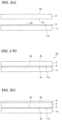
Fig. 1(a) shows asupport substrate 1 and group-13nitride crystal substrate 2,Fig. 1(b) shows abonded substrate 3 of thesupport substrate 1 and group-13nitride crystal substrate 2, andFig. 1(c) shows the state that an epitaxial film 4 is film-formed on the group-13 nitride crystal substrate of the bonded substrate. -
Fig. 2(a) shows thesupport substrate 11, the group-13nitride crystal substrate 2 and abonding layer 5,Fig. 1(b) shows abonded substrate 13 of thesupport substrate 11 and group-13nitride crystal substrate 2, andFig. 2(c) shows the state that the epitaxial film 4 is film-formed on the group-13 nitride crystal substrate of the bonded substrate. - The present invention is related to a bonded substrate of a support substrate and group-13 nitride crystal substrate. The bonded substrate means a substrate obtained by bonding the support substrate and group-13 nitride crystal substrate.
- According to a preferred embodiment, the support substrate is composed of gallium nitride, silicon carbide, aluminum nitride or diamond. Alternatively, the support substrate has a film composed of gallium nitride, silicon carbide, aluminum nitride or diamond, and the film is bonded with the group-13 nitride crystal substrate. These materials enhance the bonding strength to the group-13 nitride crystal substrate. In the case that the support substrate has the film composed of gallium nitride, silicon carbide, aluminum nitride, diamond-like carbon or diamond, although the material of an underlying substrate functioning as a base is not particularly limited, the material may preferably be silicon, mullite, sapphire, HICERAM, alumina, sialon, gallium nitride, silicon carbide, aluminum nitride or diamond.
- As a group-13 nitride constituting the group-13 nitride crystal substrate, gallium nitride, aluminum nitride, indium nitride or the mixed crystals thereof are listed. Specifically, GaN, AlN, InN, GaxAl1-xN (1>x>0), GaxIn1-xN (1>x>0), AlxIn1-xN (1>x>0), and GaxAlyInzN (1>x>0, 1>y>0, x+y+z=1) are listed.
- Particularly preferably, the group-13 nitride is a galliumnitride series nitride. The gallium nitride-series nitride is GaN, GaxAl1-xN (1>x≧0.5), GaxIn1-xN (1>x≧0.5), or GaxAlyInzN (1>x≧0.5: 0.5>y>0, x+y+z=1). The group-13 nitride may most preferably be gallium nitride.
- The
group 13 nitride crystal substrate contains one or more transition metal elements selected from the group consisting of zinc, iron, manganese, nickel and chromium in a concentration of 1×10¹⁷ atoms·cm-3 or higher and 1×10²¹ atoms·cm-3 or lower. Here, the group-13 nitride crystal substrate may contain two or more transition metal elements selected from the group consisting of zinc, iron, manganese, nickel, and chromium, and in this case, the total content of the two or more transition metal elements is made 1×10¹⁷ atoms·cm-3 or higher and 1×10²¹ atoms·cm-3 or lower. - According to the bonded substrate of the support substrate and group-13 nitride crystal substrate, one or more transition metal elements selected from the group consisting of zinc, iron, manganese, nickel and chromium is incorporated into the group-13 nitride crystal substrate in a concentration of 1×10¹⁷ atoms·cm-3 or higher. The bonding strength of the support substrate and group-13 nitride crystal substrate are thus considerably increased and the separation is suppressed in the case that a high temperature is applied during the subsequent film-formation step of the epitaxial film. On the viewpoint, the concentration of the one or more transition metal elements of the group-13 nitride crystal substrate may preferably be 1×10¹⁸ atoms·cm-3 or higher. Further, as too much transition metal element is doped, local reduction of crystal quality may be substantial and the flatness of the bonding surface is lowered to reduce the bonding strength. The concentration is thus made 1×10²¹ atoms·cm-3 or lower and is more preferably 1×10²⁰ atoms·cm-3 or lower.
- The concentration of the transition metal element of the group-13 nitride crystal substrate is measured by a secondary ion mass spectrometry (D-SIMS). The measurement is performed by measuring the concentration of the transition metal element in a depth of 3µm from the surface of the substrate. It is selected one normal position, at which the doped state of the transition metal element is considered to be stabilized in the vicinity of the center of the substrate, as a measuring point. The judgement of the normal position is performed by confirming, with eyes and an optical microscope, that there are no abnormal positions, such as inclusion, unevenness of color concentration or three-dimensional growth, in a region of Φ 10 mm around the measurement point.
- The value at a depth of 2µm, where the concentration is constant in the direction of the depth, is defined as the concentration of the transition metal element of the substrate.
- Among the transition metal elements, the primary ions and secondary ions of manganese, iron, nickel and chromium are detected through O2 beam and plus ions, respectively. The primary ions and secondary ions of zinc are detected through Cs ion beam and plus ions, respectively.
- Further, the measurement of impurity elements including the one or more transition metal elements on the surface of the group-13 nitride crystal substrate is performed by total reflection X-ray fluorescence analysis (TXRF method). Although the concentration of impurities including the transition metal elements on the surface of the substrate is preferably lower, it is difficult to apply a strong cleaning agent while avoiding the deterioration of the flatness of the bonding surface. Thus, on the viewpoint of assuring the flatness of the bonding surface of the nitride crystal without affecting the bonding strength, the total of the concentration of the impurities may preferably be made 6×10¹² atoms·cm-2 or higher and 1×10¹⁴ atoms·cm-2 or lower.
- According to a preferred embodiment, the bonding surface of the group-13 nitride crystal substrate and bonding surface of the support substrate are directly bonded.
- For example, according to an embodiment of
Fig. 1 , as shown inFig. 1(a) , abonding surface 1a of asupport substrate 1 andbonding surface 2a of a group-13nitride crystal substrate 2 are opposed. Thebonding surface 1a of thesupport substrate 1 andbonding surface 2a of the group-13nitride crystal substrate 2 are then subjected to surface activation and then bonded as shown inFig. 1(b) , to provide a bondedsubstrate 3. As shown inFig. 1(c) , a desired epitaxial film 4 is then film-formed on a film-formingface 2b of the group-13nitride crystal substrate 2. - Alternatively, a bonding layer may be provided between the group-13 nitride crystal substrate and support substrate.
- For example, according to an embodiment of
Fig. 2 , as shown inFig. 2(a) , abonding surface 5a of abonding layer 5 on amain face 11a of asupport substrate 11 is opposed to thebonding surface 2a of the group-13nitride crystal substrate 2. Thebonding surface 5a of thebonding layer 5 andbonding surface 2a of the group-13nitride crystal substrate 2 are then subjected to surface activation and then bonded as shown inFig. 2(b) , to obtain a bondedsubstrate 13. Then, as shown inFig. 2(c) , the desired epitaxial film 4 is film-formed on the film-formingface 2b of thegroup 13nitride crystal substrate 2. - Further, according to an example of
Fig. 2 , thebonding layer 5 is provided on themain face 11a of thesupport substrate 11, and thebonding surface 5a of thebonding layer 5 is directly bonded with thebonding surface 2a of the group-13nitride crystal substrate 2. However, the following embodiments are applicable. - (1) A bonding layer is provided on the main face of the group-13
nitride crystal substrate 2, and the bonding surface of the bonding layer is directly bonded with thebonding surface 1a of thesupport substrate 1. - (2) A first bonding layer is provided on the main face of the group-13
nitride crystal substrate 2, and a second bonding layer is provided on the main face of the support substrate. The bonding surface of the first bonding layer is directly bonded with the bonding surface of the second bonding layer. - According to a preferred embodiment, the bonding layer is composed of tantalum pentoxide, alumina, aluminum nitride, silicon carbide, sialon or Si(1-x)Ox (0.008^x^0.408). It is thereby possible to further improve the bonding strength of the support substrate and group-13 nitride crystal substrate.
- Besides, sialon is a ceramic obtained by sintering mixture of silicon nitride and alumina, and has the following composition.
- That is, sialon has a composition in which alumina is mixed into silicon nitride, and z indicates the ratio of the mixed alumina. z may more preferably be 0.5 or higher. Further, z may more preferably be 4.0 or lower.
- The present invention is particularly suitable in the case that the bonded substrate is of a large size. On the viewpoint, the outer diameter of the bonded substrate may more preferably be 4 inches or larger (100 mm or larger).
- In the case that the group-13 nitride crystal substrate and support substrate are directly bonded, although the main face of the group-13 nitride crystal substrate is not particularly limited, it may be Ga plane or N plane. Further, the bonding surface of the group-13 nitride crystal substrate may be c-plane, a-plane or m-plane of Wurtzite structure, or may be a plane inclined with respect to the c-plane, a-plane or m-plane.
- In the case that the group-13 nitride crystal substrate and support substrate are directly bonded through the bonding layer provided therebetween, although the main face of the group-13 nitride crystal substrate is not particularly limited, it may be Ga plane or N plane. Further, the bonding surface of the group-13 nitride crystal substrate may be c-plane, a-plane or m-plane of Wurtzite structure, or may be a plane inclined with respect to the c-plane, a-plane or m-plane.
- Although the method of producing the group-13 nitride crystal substrate is not particularly limited, vapor phase methods such as MOCVD (Metal Organic Chemical Vapor Deposition) method, hydride vapor phase epitaxy (HVPE) method, pulse excitation deposition (PXD) method, MBE method, sublimation method and the like and liquid phase methods such as ammonothermal method, flux method and the like are listed.
- As the epitaxial crystal grown on the bonded substrate, gallium nitride, aluminum nitride, indium nitride or the mixed crystals thereof may be listed. Specifically, GaN, AlN, InN, GaxAl1-xN (1>x>0), GaxIn1-xN (1>x>0), AlxIn1-xN (1>x>0) and GaxAlyInzN (1>x>0, 1>y>0, x+y+z=1) are listed. Further, as a functional layer provided on the bonded substrate, a rectifying element layer, switching element layer, power semiconductor layer and the like are listed in addition to a light emitting layer. Further, after the functional layer is provided on the group-13 nitride polarity surface of the self-standing substrate, the nitrogen polarity surface may be subjected to processing, for example grinding or polishing process, to reduce the thickness or the deviation of the thickness of the bonded substrate.
- Further, the temperature during the film-formation of the epitaxial film provided on the bonded substrate may preferably be 900 to 1200°C and more preferably be 950 to 1150°C. The separation is suppressed in the bonded substrate of the present invention, even in the case that it is exposed to such high temperature.
- Preferred bonding processes will be further described below.
- First, the respective bonding surfaces to be bonded (bonding surface of the group-13 nitride crystal substrate, bonding surface of the support substrate and bonding surfaces of the respective bonding layers) are flattened to obtain flattened faces. Here, the method of flattening the respective faces may be lapping (lap), chemical mechanical polishing (CMP) or the like. Further, the arithmetic average roughness Ra of the flattened face may preferably be 1.0nm or lower and more preferably be 0.5nm or lower.
- Then, the respective bonding surfaces are cleansed for removing the residue of a polishing agent and processing deformation layer. The method of cleaning the respective bonding surfaces may be wet cleaning, dry cleaning, scrub cleaning and the like, and the scrub cleaning is preferred for obtaining clean surface easily and efficiently. Although a cleaning agent for the cleaning is not particularly limited, for example, Sun Wash LH540 may be applied as the cleaning agent followed by cleaning by means of a scrub cleaning machine with mixed solution of acetone and IPA.
- Neutralized beam may be then irradiated onto the respective bonding surfaces to activate the respective bonding surfaces.
- When the surface activation is performed using the neutralized beam, it is preferred to use a system described in
Japanese Patent Publication No. 2014-086400A - In the activation step by beam irradiation, the voltage may preferably be made 0.5 to 2.0kV, and the current may preferably be made 50 to 200mA.
- Then, the activated surfaces are contacted and bonded with each other under vacuum atmosphere. The temperature at this time may be ambient temperature, specifically 40°C or lower and more preferably 30°C or lower. Further, the temperature during the bonding may more preferably be 20°C or higher and 25°C or lower. The applied pressure at the bonding is preferably 100 to 20000N.
- The bonded
body 3 was fabricated according to the method described referring toFig. 1 . - Specifically, a seed crystal film composed of gallium nitride was provided on an underlying substrate composed of sapphire to provide a gallium nitride template (diameter of the substrate was 4.0 inches). The thickness of the seed crystal film was made 2µm.
- A gallium nitride crystal layer of a thickness of 1mm was then formed by Na flux method. The gallium nitride crystal layer was then separated by laser lift-off method to obtain a gallium
nitride crystal substrate 2 having a thickness of 1mm. - Further, a
support substrate 1 composed of aluminum nitride sintered body and having a thickness of 0.5mm was prepared. - The
bonding surface 2a of the galliumnitride crystal substrate 2 andbonding surface 1a of the support substrate were polished, respectively, until the arithmetic surface roughnesses Ra was made 0.2nm. - Neutralized beams were then irradiated onto the
bonding surface 2a of the galliumnitride crystal substrate 2 andbonding surface 1a of thesupport substrate 1, respectively, to activate the respective bonding surfaces, which were directly bonded. - Specifically, after the respective bonding surface were cleansed to remove contamination, the gallium
nitride crystal substrate 2 and supportsubstrate 1 were introduced into a vacuum chamber. After the inside of the vacuum chamber was suctioned into vacuum of the order of 10-6Pa, high-speed atomic beam (acceleration voltage of 1 kV and Ar flow rate of 27sccm) was irradiated onto the respective bonding surfaces over 120 seconds. After thebonding surface 2a of the galliumnitride crystal substrate 2 andbonding surface 1a of thesupport substrate 1 were then contacted, pressurization at 10000N was performed over 2 minutes to perform the bonding. - However, according to the present example, zinc metal was added into a melt for performing the Na flax method, so that zinc was incorporated into the gallium
nitride crystal substrate 2 in a concentration shown in table 1. - The bonding strengths of the thus obtained boded bodies were measured by crack opening method and the results were shown in table 1. However, in the case that the bonding strength exceeds 1.75J/m2, it is described as "Bulk fracture".
- SIMS analysis was performed to determine the respective concentrations of manganese, iron, nickel, chromium and zinc contained in the gallium
nitride crystal substrate 2. The total of the thus obtained concentrations of the respective elements was calculated and shown in table 1 as the concentration of transition metal elements. - The respective bonded bodies shown in tables 1 and 2 were produced as the inventive example 1. However, the outer diameter of the bonded substrate, material of the
group 13 nitride crystal substrate, material of the support substrate, and kind and concentration of the transition metal element contained in the group-13 nitride crystal substrate were changed as shown in tables 1 and 2. The bonding strength of the thus obtained bonded body was considerably improved and the separation was not observed between the gallium nitride crystal substrate and support substrate even after MOCVD process. The results of the measurement of the bonding strengths were shown in tables 1 and 2.Table 1 Inv. Ex. 1 Inv. Ex. 2 Inv. Ex. 3 Inv. Ex. 4 Inv. Ex. 5 Inv. Ex. 6 Outer diameter 4 inches 4 inches 4 inches 4 inches 4 inches 4 inches Group 13 nitride crystal substrate GaN GaN GaN GaN GaN GaN Support substrate AlN SiC Diamond AIN AIN AIN Transition Metal Element Zn Zn Zn Zn Mn Fe, Ni, Cr Concentration of Transition Metal Element (atoms cm-3) 1×10¹⁹ 1×10¹⁹ 7×10¹⁸ 2×10¹⁹ 1×10¹⁹ 1×10¹⁹ Bonding Strength (J/m2) Bulk fracture Bulk fracture Bulk fracture Bulk fracture Bulk fracture Bulk fracture Table 2 Inv. Ex. 7 Inv. Ex. 8 Inv. Ex. 9 Inv. Ex. 10 Inv. Ex. 11 Inv. Ex. 12 Inv. Ex. 13 Outer diameter 4 inches 4 inches 4 inches 4 inches 4 inches 4 inches 4 inches Group III nitride crystal substrate GaN GaN GaN GaN GaN GaN GaN Support substrate diamond/ Si AlN/ sapphire AlN AlN AlN AlN AlN Transition Metal Element Zn Zn Zn Zn Zn Zn Zn, Fe, Mn, Cr Concentration of Transition Metal Element (atoms cm-3) 1×10¹⁹ 7×10¹⁸ 1×10¹⁷ 1×10¹⁸ 1×10²⁰ 1×10²¹ 6×10¹⁸ Bonding Strength (J/m2) Bulk fracture Bulk fracture 1.75 Bulk Fracture Bulk Fracture 1.75 Bulk Fracture - As shown in tables 1 and 2, according to the present invention, the bonding strength of the bonded substrate was considerably improved to result in bulk fracture.
- The respective bonded substrates shown in table 3 were produced as the inventive example 1. However, the outer diameter of the bonded substrate, material of the group-13 nitride crystal substrate, material of the support substrate, and kind and concentration of the element contained in the group-13 nitride crystal substrate were changed as shown in table 3. The bonding strength of the thus obtained bonded body was low and the separation occurred between the gallium nitride crystal substrate and support substrate after the MOCVD process. The results of measurement of the bonding strengths were shown in table 3.
Table 3 Com. Ex. 1 Com. Ex. 2 Com. Ex. 3 Com. Ex. 4 Outer diameter 4 inches 4 inches 4 inches 4 inches Group 13 nitride crystal substrate GaN GaN GaN GaN Support substrate AlN AIN AlN AlN Element Si Ge Zn Zn Concentration of Element (atoms cm-3) 1×10¹⁹ 1×10¹⁹ 8×10¹⁶ 2×10²¹ Bonding Strength (J/m2) 0.75 0.75 1.2 1.0 - As a result, according to the comparative examples 1 and 2, as Si or germanium was applied as the element contained in the gallium nitride crystal substrate, the bonding strength was considerably lower compared with those in the inventive examples even in the case the concentration range of the present invention was satisfied.
- Further, according to the comparative examples 3 and 4, zinc was applied as the element contained in the gallium nitride crystal substrate as the inventive example 1. However, as the concentration was out of the concentration range of the present invention, the bonding strength was considerably reduced compared with those of the inventive examples.
- Further, the concentrations of impurity elements (silicon, chlorine, manganese, iron, copper and zinc) on the surface of the gallium nitride crystal substrate in each inventive example were measured by total internal reflection X-ray fluorescence analysis (TXRF method). The surfaces of the gallium nitride crystal substrates in the respective inventive examples were subjected to cleaning before the bonding. Then, the central part (about Φ of 1 cm) of the surface of the gallium nitride crystal substrate of each inventive example was measured by TXRF method to prove that the total concentrations were 8×10¹² to 5×10¹³ atoms·cm-2.
Claims (10)
- A bonded substrate comprising a support substrate and a 13-group nitride crystal substrate,
wherein said group-13 nitride crystal substrate comprises one or more transition metal elements selected from the group consisting of zinc, iron, manganese, nickel and chromium in a concentration of 1×10¹⁷ atoms·cm-3 or higher and 1×10²¹ atoms·cm-3 or lower. - The bonded substrate of claim 1, wherein a bonding surface of said group-13 nitride crystal substrate and a bonding surface of said support substrate are directly bonded.
- The bonded substrate of claim 2, wherein said bonding surface of said group-13 nitride crystal substrate and said bonding surface of said support substrate are directly bonded by a surface activation method.
- The bonded substrate of claim 3, wherein said bonding surface of said group-13 nitride crystal substrate and said bonding surface of said support substrate are subjected to surface activation through a neutralized atomic beam.
- The bonded substrate of claim 1, further comprising a bonding layer present between said group-13 nitride crystal substrate and said support substrate.
- The bonded substrate of claim 5, wherein said bonding layer comprises tantalum pentoxide, alumina, aluminum nitride, silicon carbide, sialon or Si(1-x)Ox (0.008 ≦ x ≦ 0.408).
- The bonded substrate of any one of claims 1 to 6, wherein said group-13 nitride crystal substrate comprises gallium nitride.
- The bonded substrate of any one of claims 1 to 7, wherein said support substrate comprises gallium nitride, silicon carbide, aluminum nitride or diamond.
- The bonded substrate of any one of claims 1 to 7,wherein said support substrate comprises a film comprising gallium nitride, silicon carbide, aluminum nitride, diamond-like carbon or diamond, andwherein said film is bonded with said group-13 nitride crystal substrate.
- The bonded substrate of any one of claims 1 to 9, wherein said bonded substrate has an outer diameter of 4 inches or larger.
Applications Claiming Priority (2)
| Application Number | Priority Date | Filing Date | Title |
|---|---|---|---|
| JP2021153852 | 2021-09-22 | ||
| PCT/JP2022/019033 WO2023047691A1 (en) | 2021-09-22 | 2022-04-27 | Bonded substrate composed of support substrate and group-13 element nitride crystal substrate |
Publications (2)
| Publication Number | Publication Date |
|---|---|
| EP4407655A1 true EP4407655A1 (en) | 2024-07-31 |
| EP4407655A4 EP4407655A4 (en) | 2025-07-02 |
Family
ID=85720378
Family Applications (1)
| Application Number | Title | Priority Date | Filing Date |
|---|---|---|---|
| EP22872450.6A Pending EP4407655A4 (en) | 2021-09-22 | 2022-04-27 | Bonded substrate comprising a support substrate and a group 13 element nitride crystal substrate |
Country Status (5)
| Country | Link |
|---|---|
| US (1) | US12359341B2 (en) |
| EP (1) | EP4407655A4 (en) |
| JP (1) | JP7295351B1 (en) |
| CN (1) | CN117897797A (en) |
| WO (1) | WO2023047691A1 (en) |
Families Citing this family (3)
| Publication number | Priority date | Publication date | Assignee | Title |
|---|---|---|---|---|
| WO2024004314A1 (en) * | 2022-06-30 | 2024-01-04 | 日本碍子株式会社 | Composite substrate, and substrate for epitaxially growing group 13 element nitride |
| JP7879628B2 (en) * | 2022-09-12 | 2026-06-24 | 公立大学法人大阪 | Semiconductor substrate, semiconductor stacked structure, semiconductor device, method for manufacturing a semiconductor substrate, method for manufacturing a semiconductor stacked structure, and method for manufacturing a semiconductor device |
| KR20260077863A (en) | 2023-11-01 | 2026-05-28 | 엔지케이 가부시키가이샤 | Composite substrate and device |
Family Cites Families (13)
| Publication number | Priority date | Publication date | Assignee | Title |
|---|---|---|---|---|
| TW480554B (en) | 1999-07-22 | 2002-03-21 | Semiconductor Energy Lab | Semiconductor device and manufacturing method thereof |
| JP4458116B2 (en) * | 2007-05-30 | 2010-04-28 | 住友電気工業株式会社 | Group III nitride semiconductor layer bonded substrate for epitaxial layer growth and semiconductor device |
| JP2010168227A (en) * | 2009-01-20 | 2010-08-05 | Ngk Insulators Ltd | METHOD FOR PRODUCING Mn-DOPED GaN CRYSTAL |
| JP2010287731A (en) * | 2009-06-11 | 2010-12-24 | Sumitomo Electric Ind Ltd | Substrate product manufacturing method, substrate product, and semiconductor device |
| JP2011020896A (en) * | 2009-07-16 | 2011-02-03 | Ngk Insulators Ltd | GROUP 3B NITRIDE CRYSTAL DOPED WITH Zn, METHOD FOR PRODUCING THE SAME, AND ELECTRONIC DEVICE |
| JP2012116741A (en) | 2010-11-12 | 2012-06-21 | Sumitomo Electric Ind Ltd | Group iii nitride composite substrate |
| JP2012124473A (en) * | 2010-11-15 | 2012-06-28 | Ngk Insulators Ltd | Composite substrate and method for manufacturing the same |
| JP2014086400A (en) | 2012-10-26 | 2014-05-12 | Mitsubishi Heavy Ind Ltd | High speed atom beam source and normal temperature bonding device including the same |
| US9650723B1 (en) * | 2013-04-11 | 2017-05-16 | Soraa, Inc. | Large area seed crystal for ammonothermal crystal growth and method of making |
| WO2016106231A1 (en) * | 2014-12-22 | 2016-06-30 | Sunedison Semiconductor Limited | Manufacture of group iiia-nitride layers on semiconductor on insulator structures |
| JP6915591B2 (en) * | 2018-06-13 | 2021-08-04 | 信越化学工業株式会社 | Manufacturing method of GaN laminated board |
| KR102596121B1 (en) * | 2018-10-17 | 2023-10-30 | 엔지케이 인슐레이터 엘티디 | Junction and elastic wave device |
| US12091771B2 (en) * | 2020-02-11 | 2024-09-17 | Slt Technologies, Inc. | Large area group III nitride crystals and substrates, methods of making, and methods of use |
-
2022
- 2022-04-27 WO PCT/JP2022/019033 patent/WO2023047691A1/en not_active Ceased
- 2022-04-27 EP EP22872450.6A patent/EP4407655A4/en active Pending
- 2022-04-27 CN CN202280057051.0A patent/CN117897797A/en active Pending
- 2022-04-27 JP JP2023504559A patent/JP7295351B1/en active Active
-
2024
- 2024-02-22 US US18/584,227 patent/US12359341B2/en active Active
Also Published As
| Publication number | Publication date |
|---|---|
| WO2023047691A1 (en) | 2023-03-30 |
| JPWO2023047691A1 (en) | 2023-03-30 |
| CN117897797A (en) | 2024-04-16 |
| JP7295351B1 (en) | 2023-06-20 |
| US12359341B2 (en) | 2025-07-15 |
| US20240191394A1 (en) | 2024-06-13 |
| EP4407655A4 (en) | 2025-07-02 |
Similar Documents
| Publication | Publication Date | Title |
|---|---|---|
| JP5407385B2 (en) | Composite substrate, epitaxial substrate, semiconductor device and composite substrate manufacturing method | |
| US12359341B2 (en) | Bonded substrate composed of support substrate and group-13 element nitride crystal substrate | |
| US11094537B2 (en) | Group III nitride composite substrate and method for manufacturing the same, and method for manufacturing group III nitride semiconductor device | |
| US8101968B2 (en) | Group III nitride substrate, epitaxial layer-provided substrate, methods of manufacturing the same, and method of manufacturing semiconductor device | |
| KR101797428B1 (en) | Single-crystal diamond growth base material and method for manufacturing single-crystal diamond substrate | |
| US9136337B2 (en) | Group III nitride composite substrate and method for manufacturing the same, laminated group III nitride composite substrate, and group III nitride semiconductor device and method for manufacturing the same | |
| TWI600178B (en) | III -nitride composite substrate, a method of manufacturing the same, a laminated III-nitride compound substrate, a group III nitride semiconductor device, and a method of fabricating the same | |
| EP2154709A2 (en) | Method of manufacturing group III nitride semiconductor layer bonded substrate | |
| JP6232853B2 (en) | Group III nitride composite substrate and method for manufacturing the same, laminated group III nitride composite substrate, group III nitride semiconductor device and method for manufacturing the same | |
| JP5682651B2 (en) | Semiconductor device and manufacturing method thereof | |
| JP6146042B2 (en) | Group III nitride composite substrate and method for manufacturing the same, laminated group III nitride composite substrate, group III nitride semiconductor device and method for manufacturing the same | |
| JP2014157979A (en) | Group iii nitride composite substrate, method for manufacturing the same, lamination group iii nitride composite substrate, group iii nitride semiconductor device and method for manufacturing the same | |
| JP2014157983A (en) | Group iii nitride composite substrate, method for manufacturing the same, lamination group iii nitride composite substrate, group iii nitride semiconductor device and method for manufacturing the same | |
| JP6094243B2 (en) | Composite substrate and method for manufacturing semiconductor wafer using the same | |
| WO2025196960A1 (en) | Laminated substrate, semiconductor element, and method for manufacturing semiconductor element | |
| CN118591662A (en) | Group III nitride semiconductor substrate, epitaxial substrate, and functional device |
Legal Events
| Date | Code | Title | Description |
|---|---|---|---|
| STAA | Information on the status of an ep patent application or granted ep patent |
Free format text: STATUS: THE INTERNATIONAL PUBLICATION HAS BEEN MADE |
|
| PUAI | Public reference made under article 153(3) epc to a published international application that has entered the european phase |
Free format text: ORIGINAL CODE: 0009012 |
|
| STAA | Information on the status of an ep patent application or granted ep patent |
Free format text: STATUS: REQUEST FOR EXAMINATION WAS MADE |
|
| 17P | Request for examination filed |
Effective date: 20240328 |
|
| AK | Designated contracting states |
Kind code of ref document: A1 Designated state(s): AL AT BE BG CH CY CZ DE DK EE ES FI FR GB GR HR HU IE IS IT LI LT LU LV MC MK MT NL NO PL PT RO RS SE SI SK SM TR |
|
| DAV | Request for validation of the european patent (deleted) | ||
| DAX | Request for extension of the european patent (deleted) | ||
| A4 | Supplementary search report drawn up and despatched |
Effective date: 20250604 |
|
| RIC1 | Information provided on ipc code assigned before grant |
Ipc: H01L 21/20 20060101ALI20250528BHEP Ipc: H01L 21/18 20060101ALI20250528BHEP Ipc: H01L 21/02 20060101AFI20250528BHEP |