EP4407652A1 - Fünfdimensionales elektronenmikroskop und analyseverfahren dafür - Google Patents
Fünfdimensionales elektronenmikroskop und analyseverfahren dafür Download PDFInfo
- Publication number
- EP4407652A1 EP4407652A1 EP22872688.1A EP22872688A EP4407652A1 EP 4407652 A1 EP4407652 A1 EP 4407652A1 EP 22872688 A EP22872688 A EP 22872688A EP 4407652 A1 EP4407652 A1 EP 4407652A1
- Authority
- EP
- European Patent Office
- Prior art keywords
- dimensional
- electron
- pulses
- sample
- data
- Prior art date
- Legal status (The legal status is an assumption and is not a legal conclusion. Google has not performed a legal analysis and makes no representation as to the accuracy of the status listed.)
- Pending
Links
Images







Classifications
-
- H—ELECTRICITY
- H01—ELECTRIC ELEMENTS
- H01J—ELECTRIC DISCHARGE TUBES OR DISCHARGE LAMPS
- H01J37/00—Discharge tubes with provision for introducing objects or material to be exposed to the discharge, e.g. for the purpose of examination or processing thereof
- H01J37/26—Electron or ion microscopes; Electron or ion diffraction tubes
- H01J37/295—Electron or ion diffraction tubes
-
- G—PHYSICS
- G01—MEASURING; TESTING
- G01N—INVESTIGATING OR ANALYSING MATERIALS BY DETERMINING THEIR CHEMICAL OR PHYSICAL PROPERTIES
- G01N23/00—Investigating or analysing materials by the use of wave or particle radiation, e.g. X-rays or neutrons, not covered by groups G01N3/00 – G01N17/00, G01N21/00 or G01N22/00
- G01N23/02—Investigating or analysing materials by the use of wave or particle radiation, e.g. X-rays or neutrons, not covered by groups G01N3/00 – G01N17/00, G01N21/00 or G01N22/00 by transmitting the radiation through the material
- G01N23/04—Investigating or analysing materials by the use of wave or particle radiation, e.g. X-rays or neutrons, not covered by groups G01N3/00 – G01N17/00, G01N21/00 or G01N22/00 by transmitting the radiation through the material and forming images of the material
-
- H—ELECTRICITY
- H01—ELECTRIC ELEMENTS
- H01J—ELECTRIC DISCHARGE TUBES OR DISCHARGE LAMPS
- H01J37/00—Discharge tubes with provision for introducing objects or material to be exposed to the discharge, e.g. for the purpose of examination or processing thereof
- H01J37/02—Details
- H01J37/04—Arrangements of electrodes and associated parts for generating or controlling the discharge, e.g. electron-optical arrangement or ion-optical arrangement
- H01J37/06—Electron sources; Electron guns
- H01J37/073—Electron guns using field emission, photo emission, or secondary emission electron sources
-
- H—ELECTRICITY
- H01—ELECTRIC ELEMENTS
- H01J—ELECTRIC DISCHARGE TUBES OR DISCHARGE LAMPS
- H01J37/00—Discharge tubes with provision for introducing objects or material to be exposed to the discharge, e.g. for the purpose of examination or processing thereof
- H01J37/02—Details
- H01J37/22—Optical, image processing or photographic arrangements associated with the tube
- H01J37/226—Optical arrangements for illuminating the object; optical arrangements for collecting light from the object
- H01J37/228—Optical arrangements for illuminating the object; optical arrangements for collecting light from the object whereby illumination or light collection take place in the same area of the discharge
-
- H—ELECTRICITY
- H01—ELECTRIC ELEMENTS
- H01J—ELECTRIC DISCHARGE TUBES OR DISCHARGE LAMPS
- H01J37/00—Discharge tubes with provision for introducing objects or material to be exposed to the discharge, e.g. for the purpose of examination or processing thereof
- H01J37/02—Details
- H01J37/244—Detectors; Associated components or circuits therefor
-
- H—ELECTRICITY
- H01—ELECTRIC ELEMENTS
- H01J—ELECTRIC DISCHARGE TUBES OR DISCHARGE LAMPS
- H01J37/00—Discharge tubes with provision for introducing objects or material to be exposed to the discharge, e.g. for the purpose of examination or processing thereof
- H01J37/26—Electron or ion microscopes; Electron or ion diffraction tubes
-
- H—ELECTRICITY
- H01—ELECTRIC ELEMENTS
- H01J—ELECTRIC DISCHARGE TUBES OR DISCHARGE LAMPS
- H01J37/00—Discharge tubes with provision for introducing objects or material to be exposed to the discharge, e.g. for the purpose of examination or processing thereof
- H01J37/26—Electron or ion microscopes; Electron or ion diffraction tubes
- H01J37/28—Electron or ion microscopes; Electron or ion diffraction tubes with scanning beams
-
- H—ELECTRICITY
- H01—ELECTRIC ELEMENTS
- H01J—ELECTRIC DISCHARGE TUBES OR DISCHARGE LAMPS
- H01J37/00—Discharge tubes with provision for introducing objects or material to be exposed to the discharge, e.g. for the purpose of examination or processing thereof
- H01J37/26—Electron or ion microscopes; Electron or ion diffraction tubes
- H01J37/295—Electron or ion diffraction tubes
- H01J37/2955—Electron or ion diffraction tubes using scanning ray
-
- H—ELECTRICITY
- H01—ELECTRIC ELEMENTS
- H01J—ELECTRIC DISCHARGE TUBES OR DISCHARGE LAMPS
- H01J2237/00—Discharge tubes exposing object to beam, e.g. for analysis treatment, etching, imaging
- H01J2237/04—Means for controlling the discharge
- H01J2237/043—Beam blanking
-
- H—ELECTRICITY
- H01—ELECTRIC ELEMENTS
- H01J—ELECTRIC DISCHARGE TUBES OR DISCHARGE LAMPS
- H01J2237/00—Discharge tubes exposing object to beam, e.g. for analysis treatment, etching, imaging
- H01J2237/06—Sources
- H01J2237/063—Electron sources
- H01J2237/06325—Cold-cathode sources
- H01J2237/06333—Photo emission
-
- H—ELECTRICITY
- H01—ELECTRIC ELEMENTS
- H01J—ELECTRIC DISCHARGE TUBES OR DISCHARGE LAMPS
- H01J2237/00—Discharge tubes exposing object to beam, e.g. for analysis treatment, etching, imaging
- H01J2237/26—Electron or ion microscopes
- H01J2237/2614—Holography or phase contrast, phase related imaging in general, e.g. phase plates
-
- H—ELECTRICITY
- H01—ELECTRIC ELEMENTS
- H01J—ELECTRIC DISCHARGE TUBES OR DISCHARGE LAMPS
- H01J2237/00—Discharge tubes exposing object to beam, e.g. for analysis treatment, etching, imaging
- H01J2237/26—Electron or ion microscopes
- H01J2237/28—Scanning microscopes
- H01J2237/2802—Transmission microscopes
-
- H—ELECTRICITY
- H01—ELECTRIC ELEMENTS
- H01J—ELECTRIC DISCHARGE TUBES OR DISCHARGE LAMPS
- H01J2237/00—Discharge tubes exposing object to beam, e.g. for analysis treatment, etching, imaging
- H01J2237/26—Electron or ion microscopes
- H01J2237/28—Scanning microscopes
- H01J2237/2803—Scanning microscopes characterised by the imaging method
Definitions
- the present invention relates to a five-dimensional electron microscope, and relates specifically to a method for analyzing distortion and magnetization mapping with respect to observation data of the five-dimensional electron microscope.
- an electron Since an electron has double properties of wave and particle, the electron can be accelerated to have a wavelength of pico-meter level, and can be made to converge to form an image in a real space. Since the transmission electron microscope (TEM), the scanning transmission electron microscope (STEM), and the aberration correction TEM have made a remarkable advancement, high resolution imaging reaching a sub-angstrom scale is currently enabled. Since electron diffraction analysis, tomography, and single particle imaging have advanced, the electron microscope is currently becoming a central means in many fields from material science to biology. In many electron microscopes, electrons are generated thermally by heating a cathode, or are generated also by field emission. In these electron microscopes, although the temporal resolution reaches millisecond or more although it is restricted by the video rate of the detector, and high spatial resolution can be maintained on the other hand.
- PTL 1 relates to a four-dimensional ultrafast electron microscope (UEM) in-situ imaging with ultrafast temporal resolution in TEM, and there is disclosed a technique where single electron imaging is used as a component of the four-dimensional UEM technique and high spatial and temporal resolution are provided.
- UEM ultrafast electron microscope
- PTL 1 relates to methods and systems for a convergent beam UEM focusing the electron beams onto the sample to measure the structural characteristics in three dimensions as a function of time, discloses that not only four-dimensional imaging of the samples but also characterization of electron energy are provided and that time resolved electron energy loss spectroscopy is performed, however there is no disclosure on the implementation method and the analysis method for the five-dimensional electron microscope.
- An object of the present invention is to solve the problem described above and to provide a five-dimensional electron microscope and an analysis method for it.
- the present invention provides a five-dimensional electron microscope including a photocathode that is irradiated with first laser pulses and generates electron pulses, a sample that is irradiated with the electron pulses and second laser pulses, and becomes excited, a pixel camera that detects electron pulses that have passed through the sample, and a processing unit that processes an output of the pixel camera, and the electron pulses are delayed from the second laser pulses by a predetermined delay time.
- the present invention provides an analysis method for a five-dimensional electron microscope, the analysis method including steps of irradiating first laser pulses onto a photocathode to generate electron pulses, irradiating second laser pulses and electron pulses to a sample to excite the sample, the electron pulses being delayed from the second laser pulses by a predetermined delay time, detecting the electron pulses that have passed through the sample by a pixel camera, processing an output of the pixel camera, and thereby analyzing the sample.
- imaging of five-dimensional information is enabled by using a pixel camera.
- the present embodiment is an embodiment of a 5D-STEM system capable of obtaining images ultrafast temporally resolved, uses a pixel camera (ultra high performance imaging device) capable of imaging a fast moving image as a camera of the electron microscope, includes a laser optical system, a transmission electron microscope, a pixel camera, and software integrating them, and enables imaging of five-dimensional information.
- a pixel camera ultra high performance imaging device
- "fast” is defined corresponding to an oscillating frequency of a scan coil.
- the present invention is an embodiment of a five-dimensional electron microscope and an observation method of it, the five-dimensional electron microscope including a photocathode that is irradiated with first laser pulses and generates electron pulses, a sample that is irradiated with electron pulses and second laser pulses, and becomes excited, a pixel camera that detects electron pulses that have passed through the sample, and a processing unit that processes an output of the pixel camera, the electron pulses being delayed from the second laser pulses by a predetermined delay time.
- the transmission electron microscope includes a scan coil enabling electron beam scanning, and includes a window and a mirror guiding laser pulses to a photocathode and a sample.
- a femtosecond laser or a nanosecond laser By selecting a femtosecond laser or a nanosecond laser, it is possible to perform temporal resolution measurement in a wide temporal scale from a femtosecond to a nanosecond.
- repetition frequency of the pulse laser is set between 1 kHz to 1 MHz.
- a laser light of a near-infrared region or a laser light whose wavelength is converted using a non-linear optical element it is required that the pixel camera can load two-dimensional data within the time of approximately a millisecond.
- the pixel camera is required to be a camera employing a direct detection method in order to measure a minute electron pulse with high sensitivity.
- FIG. 1 is a schematic drawing of a five-dimensional electron microscope in a femtosecond experimental mode related to the first embodiment.
- a femtosecond laser 1A is divided into two beams, and is introduced to an electron microscope (STEM) 26 including a scan coil.
- STEM electron microscope
- One is used for electron pulse generation, the other is used for sample excitation, and the delay time between two pulses is mechanically controlled by a delay generator 25.
- a laser light having energy higher than that of a work function of a photocathode (LaB6 and metal) 9. It is capable of obtaining ultrafast moving image of nano-material 28 by the pixel camera 18.
- LaB6 and metal photocathode
- an output of the pixel camera 18 is converted to the ultrafast moving image 28 by predetermined image processing by a processing unit including a central processing unit (CPU) and the like.
- An electron energy loss spectroscopic detector 27 is used for analyzing the element composition and the chemical bonding state of a sample 15.
- the processing unit performs not only image processing but also control of operation of the electron microscope 26 such as scanning of electron pulses.
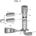
- FIG. 2 is a schematic drawing of a five-dimensional electron microscope in a nanosecond experimental mode related to the first embodiment.
- the nanosecond experimental mode laser pulses generated from two sets of nanosecond lasers 1B are used for electron pulse generation and sample excitation respectively, and the delay time between two pulses is electrically controlled by the delay generator 25.
- STEM observation is performed using converged electron pulses of the electron microscope 26, and temporal resolution observation based on the stroboscopic pump-probe principle is performed by controlling the delay time with respect to the laser pulses.
- FIG. 3 illustrates concrete configuration elements of a five-dimensional electron microscope system in a femtosecond experimental mode related to the present embodiment.
- a laser light from the femtosecond laser 1A passes through a 1/2 wavelength plate 2, is divided by a cube beam splitter 3, each enters windows 7, 23 of the electron microscope 26 through wavelength conversion devices 4, 20, beam expanders 5,21, and lenses 6, 22 respectively, and performs electron pulse generation and sample excitation.
- Electrons generated by the photocathode 9 by irradiation of the laser light reflected by a mirror 8 is accelerated by an accelerator 10, and is thereafter irradiated onto the sample 15 through an optical system including a condenser lens 11, a condenser mini-lens 12, a deflection coil 13 that is a deflection unit for scanning electron pulses, and an object lens 14.
- electrons having passed through the sample 15 excited by the laser light reflected by a mirror 24 go through an object lens 16 and an imaging system lens 17, and are imaged by the pixel camera 18.
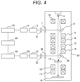
- FIG. 4 illustrates concrete configuration elements of a five-dimensional electron microscope system in a nanosecond experimental mode related to the present embodiment.
- laser pulses generated from two sets of the nanosecond lasers 1B are used for electron pulse generation and sample excitation respectively, and the delay time between two pulses is electrically controlled by the delay generator 25.
- the configuration of the electron microscope 26 is same to that illustrated in FIG. 3 .
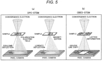
- FIG. 5 An analysis method of the five-dimensional electron microscope of the present embodiment is illustrated schematically in FIG. 5 .
- DPC-STEM method differential phase contrast method
- CBED-STEM method converged beam electron diffraction method
- a DPC-STEM method called a four-dimensional STEM illustrated in FIG. 5 (a) and using a pixel camera
- CBED-STEM method illustrated in FIG. 5 (b) a DPC-STEM method
- various physical quantity such as the magnetization vector, electric field polarization, lattice constant, distortion, and inclination angle can be acquired quantitatively.
- the data obtained by combination of these methods and the stroboscopic pump-probe method are five-dimensional data combining two dimension of the sample surface, two dimension of the reciprocal lattice space, and one dimension of the time.
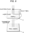
- FIG. 6 illustrates a schematic drawing of a pump-probe method in electron microscope observation method of the present embodiment.
- Electron pulses and laser pulses are irradiated generally coaxially to the sample 15 of a thin piece through which the electron beam of the electron microscope can pass through.
- Response of the sample 15 excited by the laser pulses is observed by the electron pulses irradiated to be delayed by the delay time t.
- the electron pulses having passed through the sample 15 is detected as two-dimensional image data by the pixel camera 18 located behind the sample 15.
- a method specialized in observing a reversible response to a stimulus is the stroboscopic pump-probe method.
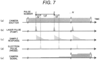
- FIG. 7 illustrates an observation procedure of the stroboscopic pump-probe method.
- the waveforms of (a) to (e) of FIG. 7 illustrate the camera shutter, laser pulse, sample response, electron pulse, and camera signal respectively.
- FIG. 7 (a) firstly, the shutter of the camera of the transmission electron microscope is opened, and exposure is started.
- FIG. 7 (b) laser pulses are repeatedly irradiated onto the sample 15 to impart stimuli.
- the sample repeats same responses every time against the stimuli, and is required to be entirely relaxed until the time when next laser pulse is irradiated (an inverse number of the repetition frequency f).
- the electron pulse is irradiated to the sample, and electrons having passed through the sample 15 are detected by the camera 18.
- the electron pulse illustrated in FIG. 7 (d) is configured of less number of piece of electrons of one to 1,000 approximately, in order to obtain an image with sufficient contrast, many cumulating number of times are necessary.
- utilizing periodicity of the laser phenomena are repeated to cumulate the camera signals, and the shutter is closed when sufficient signals are obtained as illustrated in FIG. 7 (e) .
- the causes limiting the overall temporal resolution within this series of processes are three points of the time width of the laser pulse, the time width of the electron pulse, and accuracy of the delay time. In fact, the overall temporal resolution is often determined by the time width of the electron pulse.
- imaging of a moving image by a high-speed camera of a prior art had a problem that the temporal resolution was limited to approximately a millisecond by the shutter speed of a camera, according to the stroboscopic pump-probe method of the present embodiment, since the temporal resolution does not depend on the shutter speed of a camera but depends on pulse property of the laser and electron, imaging of an ultrafast moving image is enabled.
- the stroboscopic pump-probe method is applied to DPC-STEM method and CBED-STEM method by a scanning transmission electron microscope including a pulse laser system and a pixel camera, five-dimensional data including two-dimensional space (x, y), two-dimensional wave number space (k x , k y ), and time (t) are acquired fast, and an ultrafast moving image of nano-material is formed by a post process after acquisition of the data.
- 5D-STEM of the present embodiment by using electron pulses, the stroboscopic pump-probe method is applied to DPC-STEM method described above, and five-dimensional data where the time axis is added to four-dimensional data are acquired.
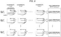
- the five-dimensional data are acquired by such procedure as illustrated in FIG. 9 .
- a pulse laser irradiated to entire sample in advance causes an excited state of the sample, convergence electron pulses are irradiated here to be delayed by delay time t0, and thereby the wave number distribution of the deflected electron in the sample coordinate (x0, y0) is acquired as two-dimensional image data.
- Electron pulses are scanned in a state of fixing the delay time t0, and similar observation is performed in an adjacent coordinate (x1, y0).
- four-dimensional data (x, y, k x , k y ) equivalent to a snap shot of a phenomenon at the delay time t0 are obtained.
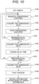
- the pulse laser irradiated to the entire sample in advance causes an excited state of the sample
- convergence electron pulses are irradiated here to be delayed by the delay time t0 (S101)
- the wave number distribution of the deflected electron in the sample coordinate (x0, y0) is acquired as two-dimensional image data (S102).
- Electron pulses are scanned in a state of fixing the delay time t0 (S103), and similar observation is performed in an adjacent coordinate (x1, y0).
- 5D-STEM of the present embodiment information on the electric field, magnetic field, and crystal lattice in a solid substance changing fast according to the external field can be obtained quantitatively.
- it is supposed to be capable of observing processes through which a magnetic wall in ferromagnetic material known as a magnetic structural body of a nano scale, a vortex in a superconductor, magnetic skyrmions in a chiral magnetic body, and so on are generated, discreated, deformed, and transported by stimuli.
- fast response by light is expected also in a ferroelectric domain in a ferroelectric substance bringing electric field distribution in a solid substance and a p-n junction interface in a semiconductor.
- FIG. 11 illustrates a data example acquired by 5D-STEM of the present embodiment.
- a state of acoustic phonon propagation in a Si thin piece after irradiating the femtosecond laser observed by CBED-STEM method is illustrated.
- Such state is known that deformation of the thin piece sample propagates radially with a wave source of a structure of metal tungsten vapor-deposited by a focused ion beam method.
- the contrast of the image expresses distortion of the thin piece sample extracted quantitatively from an electron diffraction figure.
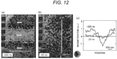
- FIG. 12 illustrates another data example acquired by 5D-STEM of the present embodiment.
- a discreating and reforming process of a magnetic wall in a FeNiPdP alloy after irradiating a nanosecond laser observed by the DPC-STEM method It is known that two pieces of the magnetic wall (white dotted line) pinned to a rectangular hole formed by a focused ion beam method form a magnetic domain structure where the direction of the magnetization vector (white arrow) differs by 180 degrees ( FIG. 12 (a) ).
- the color and intensity of the image express the direction and the absolute value of the magnetization vector.
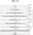
- FIG. 13 illustrates a summary of the total process of 5D-STEM of the present embodiment.
- a diffraction image (k x , k y ) within a target range of the space (x, y) and time (t) is acquired using an optical delay stage and a deflection coil within the electron microscope.
- Data obtained become five-dimensional data having five axes of (x, y, k x , k y , t).
- the present embodiment provides a data analysis method for the five-dimensional data.
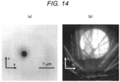
- FIG. 14 illustrates representative measurement data obtained from 5D-STEM of the present embodiment.
- t is equal to -40 ps.
- FIG. 14 (a) is a real image of a silicon sample obtained by the analysis, and a black circle at the center is a tungsten vapor-deposited region.
- FIG. 14 (b) is a convergence electron diffraction figure, the position of the line corresponds to the distortion within the sample and the position of the transmission electron (the center of the circle) corresponds to the magnitude of magnetization respectively.
- four-dimensional data recording the convergence electron diffraction figure such as FIG. 14 (b) are obtained for each point of the space of FIG. 14 (a) with respect to each clock time.
- FIG. 15 illustrates an analysis algorithm with respect to 5D-STEM of the present embodiment. As described above, since the intensity of the electron beam used in 5D-STEM is very low, analysis cannot be performed well by the method described above where an analysis method used in 4D-STEM is simply parallelized.
- pre-processing (S152) and post-processing (S154) are performed respectively.
- pre-processing (S152) four-dimensional data having been read in parallel are combined once and are made five-dimensional data.
- smoothing of the five-dimensional data along each axis of x, y, k x , k y , t the signal-to-noise ratio of the data is improved with the temporal and spatial resolution being slightly sacrificed.
- post-processing also, two-dimensional data after the physical quantity calculation are combined and are made three-dimensional data, and smoothing along each axis of x, y, t is thereafter performed.
- pre-processing and post-processing are algorithms newly added in an analysis algorithm of the present embodiment.
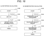
- distortion calculation the scattering angle of electrons scattered by the sample is obtained by detecting the local maximum value of the intensity profile along a certain straight line within a diffraction image. Since this scattering angle changes according to the distortion of the sample, the magnitude of the distortion at an optional position within the sample can be calculated. Also, when magnetization within the sample is to be obtained by magnetization calculation, the convergence electron beam diffraction figure is binarized by a proper threshold value, and the gravity center position of the binarized image is obtained.
- this gravity center position is equivalent to the deflection amount of an electron beam, the gravity center position is proportional to magnetization of the sample.
- a deflection amount of the electron beam when there is not a sample is deducted as the background.
- the deflection amount in k x and k y direction is stored as a complex number, and eventually becomes complex number data having axes of (x, y, t) .
- the present embodiment is enabled to calculate a meaningful physical quantity from data with a large noise measured by an electron beam of very low intensity by pre/post processing that totally takes information in the time, space, and wave number space in consideration as described above.
- FIG. 16 illustrates an example of physical quantity calculation.
- FIG. 16 (a) represents distortion calculation
- FIG. 16 (b) represents magnetization calculation.
- S160, S163 line cut
- S161 and S162 as well as threshold value processing (S164), gravity center calculation (S165), and background processing (S166) are performed respectively, and the process is finished.
- S164 threshold value processing
- S165 gravity center calculation
- S166 background processing
- FIG. 17 illustrates an example of the change of data by presence and absence of pre-processing. Compared to the diffraction image of a case without pre-processing illustrated in FIG. 17 (a) , in the data where the averaging filter of size 3 is applied to all directions of the space, wave number space, and time illustrated in FIG. 17 (b) , it is known that the signal-to-noise ratio is dramatically improved and analysis is facilitated.
- FIG. 18 illustrates an example of data expressing spatial resolution and temporal resolution related to the present embodiment.
- FIG. 18 (a) and (b) illustrate spatial resolution evaluation data observed under 2 Tesla magnetic field and under zero magnetic field.
- FIG. 18 (a) and (b) were obtained by spatial mapping of GaP/Si interface and YIG thin piece sample end by CBED.
- the curved line in the drawing expresses a step function convoluted with a Gaussian function in order to evaluate broadening by spatial resolution. 8 nanometer spatial resolution was obtained in FIG. 18 (a) , and 400 nanometer spatial resolution was obtained in FIG. 18 (b) .
- FIG. 18 (c) and (d) illustrate temporal resolution evaluation data of the cases of using a femtosecond laser and a nanosecond laser under 2 Tesla magnetic field.
- the curved line in the drawing expresses a step function convoluted with a Gaussian function in order to evaluate broadening by temporal resolution. 4 picosecond temporal resolution was obtained in FIG. 18 (c) , and 10 nanosecond temporal resolution was obtained in FIG. 18 (d) .
- the temporal resolution in both methods can be improved by 12 digits or more.
Landscapes
- Chemical & Material Sciences (AREA)
- Analytical Chemistry (AREA)
- Physics & Mathematics (AREA)
- Health & Medical Sciences (AREA)
- Life Sciences & Earth Sciences (AREA)
- Biochemistry (AREA)
- General Health & Medical Sciences (AREA)
- General Physics & Mathematics (AREA)
- Immunology (AREA)
- Pathology (AREA)
- Analysing Materials By The Use Of Radiation (AREA)
- Engineering & Computer Science (AREA)
- Computer Vision & Pattern Recognition (AREA)
Applications Claiming Priority (2)
| Application Number | Priority Date | Filing Date | Title |
|---|---|---|---|
| JP2021152759 | 2021-09-21 | ||
| PCT/JP2022/033313 WO2023047932A1 (ja) | 2021-09-21 | 2022-09-05 | 5次元電子顕微鏡及びその解析方法 |
Publications (2)
| Publication Number | Publication Date |
|---|---|
| EP4407652A1 true EP4407652A1 (de) | 2024-07-31 |
| EP4407652A4 EP4407652A4 (de) | 2025-10-22 |
Family
ID=85720581
Family Applications (1)
| Application Number | Title | Priority Date | Filing Date |
|---|---|---|---|
| EP22872688.1A Pending EP4407652A4 (de) | 2021-09-21 | 2022-09-05 | Fünfdimensionales elektronenmikroskop und analyseverfahren dafür |
Country Status (4)
| Country | Link |
|---|---|
| US (1) | US20240395499A1 (de) |
| EP (1) | EP4407652A4 (de) |
| JP (1) | JPWO2023047932A1 (de) |
| WO (1) | WO2023047932A1 (de) |
Families Citing this family (1)
| Publication number | Priority date | Publication date | Assignee | Title |
|---|---|---|---|---|
| US12313957B1 (en) * | 2022-10-26 | 2025-05-27 | United States Of America As Represented By The Secretary Of The Air Force | High speed strobe photography |
Family Cites Families (1)
| Publication number | Priority date | Publication date | Assignee | Title |
|---|---|---|---|---|
| JP2007531876A (ja) * | 2004-04-02 | 2007-11-08 | カリフォルニア インスティテュート オブ テクノロジー | 超高速光電子顕微鏡のための方法およびシステム |
-
2022
- 2022-09-05 US US18/693,713 patent/US20240395499A1/en active Pending
- 2022-09-05 JP JP2023549453A patent/JPWO2023047932A1/ja active Pending
- 2022-09-05 WO PCT/JP2022/033313 patent/WO2023047932A1/ja not_active Ceased
- 2022-09-05 EP EP22872688.1A patent/EP4407652A4/de active Pending
Also Published As
| Publication number | Publication date |
|---|---|
| EP4407652A4 (de) | 2025-10-22 |
| WO2023047932A1 (ja) | 2023-03-30 |
| JPWO2023047932A1 (de) | 2023-03-30 |
| US20240395499A1 (en) | 2024-11-28 |
Similar Documents
| Publication | Publication Date | Title |
|---|---|---|
| JP3867524B2 (ja) | 電子線を用いた観察装置及び観察方法 | |
| JP4587742B2 (ja) | 荷電粒子線顕微方法及び荷電粒子線応用装置 | |
| Crewe | The current state of high resolution scanning electron microscopy | |
| US5055679A (en) | Surface analysis method and apparatus | |
| JP6998469B2 (ja) | 電子線装置 | |
| Sheppard | The generalized microscope | |
| AU2014340580A1 (en) | System and method for compressive scanning electron microscopy | |
| JP6957641B2 (ja) | 荷電粒子線装置およびそれを用いた試料観察方法 | |
| US10593511B2 (en) | Method of determining the deflection of an electron beam resulting from an electric field and/or a magnetic field | |
| CN111982945A (zh) | 基于超快透射电镜系统获取时间分辨暗场像的方法及应用 | |
| EP4407652A1 (de) | Fünfdimensionales elektronenmikroskop und analyseverfahren dafür | |
| JP4337832B2 (ja) | 電子線を用いた観察装置及び観察方法 | |
| US4788495A (en) | Method for the indirect identification of the intensity distribution of particle beam pulses generated in a particle beam measuring instrument | |
| EP4517311A1 (de) | Differentialphasenkontrastmikroanalyse unter verwendung von energieverlustspektrometern | |
| WO2019175611A1 (en) | Measuring crystal quality in low dimensional 2d materials based on polarization resolved second harmonic generation | |
| JP2025097962A (ja) | 荷電粒子ビーム及びアクティブピクセル制御センサを使用して試料を分析するためのシステム及び方法 | |
| JP2015056376A (ja) | 走査透過電子顕微鏡及びその収差測定方法 | |
| DE112017007862T5 (de) | Ladungsträgerstrahlvorrichtung | |
| JP2967074B2 (ja) | 荷電粒子線顕微法および荷電粒子線顕微装置 | |
| JP2001093459A (ja) | 走査透過型電子顕微鏡 | |
| Hua et al. | Extracting contrast in an X-ray speckle visibility spectroscopy experiment under imperfect conditions | |
| JPH05109379A (ja) | 走査型反射電子顕微鏡 | |
| TW202548204A (zh) | 內部形狀評估系統及內部形狀評估方法 | |
| US20250349492A1 (en) | Beam synchronization in microscopy | |
| US20250349503A1 (en) | Beam alignment and synchronization in microscopy |
Legal Events
| Date | Code | Title | Description |
|---|---|---|---|
| STAA | Information on the status of an ep patent application or granted ep patent |
Free format text: STATUS: THE INTERNATIONAL PUBLICATION HAS BEEN MADE |
|
| PUAI | Public reference made under article 153(3) epc to a published international application that has entered the european phase |
Free format text: ORIGINAL CODE: 0009012 |
|
| STAA | Information on the status of an ep patent application or granted ep patent |
Free format text: STATUS: REQUEST FOR EXAMINATION WAS MADE |
|
| 17P | Request for examination filed |
Effective date: 20240422 |
|
| AK | Designated contracting states |
Kind code of ref document: A1 Designated state(s): AL AT BE BG CH CY CZ DE DK EE ES FI FR GB GR HR HU IE IS IT LI LT LU LV MC MK MT NL NO PL PT RO RS SE SI SK SM TR |
|
| DAV | Request for validation of the european patent (deleted) | ||
| DAX | Request for extension of the european patent (deleted) | ||
| A4 | Supplementary search report drawn up and despatched |
Effective date: 20250919 |
|
| RIC1 | Information provided on ipc code assigned before grant |
Ipc: H01J 37/06 20060101AFI20250915BHEP Ipc: H01J 37/20 20060101ALI20250915BHEP Ipc: H01J 37/22 20060101ALI20250915BHEP Ipc: H01J 37/244 20060101ALI20250915BHEP Ipc: H01J 37/28 20060101ALI20250915BHEP Ipc: G01N 23/04 20180101ALI20250915BHEP Ipc: H01J 37/073 20060101ALI20250915BHEP Ipc: H01J 37/26 20060101ALI20250915BHEP Ipc: H01J 37/295 20060101ALI20250915BHEP |