EP4407597A1 - Anzeigevorrichtung und verfahren zur steuerung davon - Google Patents
Anzeigevorrichtung und verfahren zur steuerung davon Download PDFInfo
- Publication number
- EP4407597A1 EP4407597A1 EP24153597.0A EP24153597A EP4407597A1 EP 4407597 A1 EP4407597 A1 EP 4407597A1 EP 24153597 A EP24153597 A EP 24153597A EP 4407597 A1 EP4407597 A1 EP 4407597A1
- Authority
- EP
- European Patent Office
- Prior art keywords
- data
- apl
- display module
- condition
- specific
- Prior art date
- Legal status (The legal status is an assumption and is not a legal conclusion. Google has not performed a legal analysis and makes no representation as to the accuracy of the status listed.)
- Pending
Links
Images


Classifications
-
- G—PHYSICS
- G09—EDUCATION; CRYPTOGRAPHY; DISPLAY; ADVERTISING; SEALS
- G09G—ARRANGEMENTS OR CIRCUITS FOR CONTROL OF INDICATING DEVICES USING STATIC MEANS TO PRESENT VARIABLE INFORMATION
- G09G5/00—Control arrangements or circuits for visual indicators common to cathode-ray tube indicators and other visual indicators
- G09G5/003—Details of a display terminal, the details relating to the control arrangement of the display terminal and to the interfaces thereto
- G09G5/006—Details of the interface to the display terminal
-
- G—PHYSICS
- G09—EDUCATION; CRYPTOGRAPHY; DISPLAY; ADVERTISING; SEALS
- G09G—ARRANGEMENTS OR CIRCUITS FOR CONTROL OF INDICATING DEVICES USING STATIC MEANS TO PRESENT VARIABLE INFORMATION
- G09G3/00—Control arrangements or circuits, of interest only in connection with visual indicators other than cathode-ray tubes
- G09G3/20—Control arrangements or circuits, of interest only in connection with visual indicators other than cathode-ray tubes for presentation of an assembly of a number of characters, e.g. a page, by composing the assembly by combination of individual elements arranged in a matrix no fixed position being assigned to or needed to be assigned to the individual characters or partial characters
- G09G3/2092—Details of a display terminals using a flat panel, the details relating to the control arrangement of the display terminal and to the interfaces thereto
- G09G3/2096—Details of the interface to the display terminal specific for a flat panel
-
- G—PHYSICS
- G09—EDUCATION; CRYPTOGRAPHY; DISPLAY; ADVERTISING; SEALS
- G09G—ARRANGEMENTS OR CIRCUITS FOR CONTROL OF INDICATING DEVICES USING STATIC MEANS TO PRESENT VARIABLE INFORMATION
- G09G3/00—Control arrangements or circuits, of interest only in connection with visual indicators other than cathode-ray tubes
- G09G3/20—Control arrangements or circuits, of interest only in connection with visual indicators other than cathode-ray tubes for presentation of an assembly of a number of characters, e.g. a page, by composing the assembly by combination of individual elements arranged in a matrix no fixed position being assigned to or needed to be assigned to the individual characters or partial characters
- G09G3/22—Control arrangements or circuits, of interest only in connection with visual indicators other than cathode-ray tubes for presentation of an assembly of a number of characters, e.g. a page, by composing the assembly by combination of individual elements arranged in a matrix no fixed position being assigned to or needed to be assigned to the individual characters or partial characters using controlled light sources
- G09G3/30—Control arrangements or circuits, of interest only in connection with visual indicators other than cathode-ray tubes for presentation of an assembly of a number of characters, e.g. a page, by composing the assembly by combination of individual elements arranged in a matrix no fixed position being assigned to or needed to be assigned to the individual characters or partial characters using controlled light sources using electroluminescent panels
- G09G3/32—Control arrangements or circuits, of interest only in connection with visual indicators other than cathode-ray tubes for presentation of an assembly of a number of characters, e.g. a page, by composing the assembly by combination of individual elements arranged in a matrix no fixed position being assigned to or needed to be assigned to the individual characters or partial characters using controlled light sources using electroluminescent panels semiconductive, e.g. using light-emitting diodes [LED]
- G09G3/3208—Control arrangements or circuits, of interest only in connection with visual indicators other than cathode-ray tubes for presentation of an assembly of a number of characters, e.g. a page, by composing the assembly by combination of individual elements arranged in a matrix no fixed position being assigned to or needed to be assigned to the individual characters or partial characters using controlled light sources using electroluminescent panels semiconductive, e.g. using light-emitting diodes [LED] organic, e.g. using organic light-emitting diodes [OLED]
-
- G—PHYSICS
- G09—EDUCATION; CRYPTOGRAPHY; DISPLAY; ADVERTISING; SEALS
- G09G—ARRANGEMENTS OR CIRCUITS FOR CONTROL OF INDICATING DEVICES USING STATIC MEANS TO PRESENT VARIABLE INFORMATION
- G09G2330/00—Aspects of power supply; Aspects of display protection and defect management
- G09G2330/02—Details of power systems and of start or stop of display operation
- G09G2330/025—Reduction of instantaneous peaks of current
-
- G—PHYSICS
- G09—EDUCATION; CRYPTOGRAPHY; DISPLAY; ADVERTISING; SEALS
- G09G—ARRANGEMENTS OR CIRCUITS FOR CONTROL OF INDICATING DEVICES USING STATIC MEANS TO PRESENT VARIABLE INFORMATION
- G09G2360/00—Aspects of the architecture of display systems
- G09G2360/16—Calculation or use of calculated indices related to luminance levels in display data
-
- G—PHYSICS
- G09—EDUCATION; CRYPTOGRAPHY; DISPLAY; ADVERTISING; SEALS
- G09G—ARRANGEMENTS OR CIRCUITS FOR CONTROL OF INDICATING DEVICES USING STATIC MEANS TO PRESENT VARIABLE INFORMATION
- G09G2370/00—Aspects of data communication
-
- G—PHYSICS
- G09—EDUCATION; CRYPTOGRAPHY; DISPLAY; ADVERTISING; SEALS
- G09G—ARRANGEMENTS OR CIRCUITS FOR CONTROL OF INDICATING DEVICES USING STATIC MEANS TO PRESENT VARIABLE INFORMATION
- G09G2370/00—Aspects of data communication
- G09G2370/04—Exchange of auxiliary data, i.e. other than image data, between monitor and graphics controller
Definitions
- the present disclosure relates to a display device, a main board, a timing controller board, etc., and more particularly, to a method of transmitting and receiving a video signal according to a serial interface system and an image processing device for implementing the same.
- An image processing device processes an image signal or data received from the outside according to various image processing processes.
- the image processing device may display the processed image data as an image on a display panel equipped with its own, or may output the image data processed to be displayed as an image on another display device equipped with a panel to the corresponding display device.
- an image processing device when it is a device capable of processing image, it may pertain to both a case of having a panel capable of displaying an image and a case of failing to have the panel.
- the former case is specifically referred to as a display device, and examples thereof include a TV, a portable multimedia player, a tablet, a mobile phone, and the like, and examples of the latter case include a set-top box, a video player, and the like.
- Image data is transmitted from a transmitting side to a receiving side by an interface of preset specifications.
- the transmitting side and the receiving side may be respectively devices or boards.
- An example of transmitting image data between the devices may include a case in which image data is outputted from an image processing device to a display device, and an example of transmitting image data between the boards may include a case of outputting image data from an image processing board to a timing controller board in a device.
- LVDS Low Voltage Differential Signaling
- Serial communication refers to a communication system that transmits one bit per cycle.
- a transmitting node transmits two signals having one bit information per cycle to an LVDS interface.
- the receiving node recognizes information by one bit through a voltage difference between the two signals.
- Differential signaling refers to a difference between two signals. Communication robust to noise may be configured by transmitting data using the differential signaling.
- the LVDS system has limitations.
- Vx1 V-by-One
- Vx1 technology adopts a clock-embedded system, which is a method of transmitting a data signal and clock information through a single signal line.
- a data signal and a clock signal are transmitted through separate signal lines, which is called a data/clock separation transmission system.
- a data/clock separation transmission system there is a problem that distortion between the data signal and the clock signal increases as a data transmission speed increases or a cable arrival distance increases.
- the data and clock signal reception timing is delayed, there is a problem that data cannot be received properly as well.
- clock information is embedded in a serial data signal.
- clock information may be extracted by a Clock Data Recovery (CDR) circuit of a de-serializer, and a data signal may be synchronized with an embedded clock.
- CDR Clock Data Recovery
- Vx1 technology has the advantage of being able to transmit data at a higher speed through a relatively longer cable.
- APL Average Picture Level
- the APL value is transferred using a control (CTL) data region in the Vx1 protocol.
- CTL control
- an OLED panel uses a frame memory to calculate APL, and enables a screen to be driven in the form of frame memory less, so that the screen can be driven only with the APL data value transferred from a main board (Main SoC).
- the present disclosure is directed to a display device and method of controlling the same that substantially obviate one or more problems due to limitations and disadvantages of the related art.
- One object of the present disclosure devised to solve the above-mentioned problems is to provide a display device and method of controlling the same, which drastically reduce the possibility of errors for APL data in an interface inside the display device.
- Another object of the present disclosure devised to solve the above-mentioned problems is to provide a display device and method of controlling the same, which provide a technology for a T-CON board to receive error-free control data (e.g., including APL values) from a main board even in the lossy structure of Vx1 protocol.
- error-free control data e.g., including APL values
- a method of controlling a display device including generating a plurality of Average Picture Level (APL) data for each specific period within a vertical blank period by a first display module, transmitting a plurality of the APL data to a second display module at a specific timing point by the first display module, receiving a plurality of the APL data by the second display module, and processing image data by the second display module based on a specific APL data among a plurality of the received APL data.
- APL Average Picture Level
- the specific period may include a case of satisfying all of a first condition that a vertical synchronization signal Vsync is in a low state, a second condition that a horizontal synchronization signal Hsync is in the low state, and a third condition that a data enable signal DE is in the low state.
- the specific timing point may include a timing point at which the vertical synchronization signal Vsync rises.
- the transmitting may include transmitting a plurality of the APL data once in a table format.
- the processing may further include comparing a plurality of the received APL data and selecting the specific APL data with most numerous equivalence.
- a first display module for processing image data may include an interface configured to connect to a second display module, a generator generating a plurality of Average Picture Level (APL) data for each specific period within a vertical blank period, and a controller controlling the interface to transmit a plurality of the APL data to a timing controller board at a specific timing point.
- APL Average Picture Level
- a second display module for processing image data may include an interface receiving a plurality of APL data from a first display module and a controller processing the image data based on a specific APL data among a plurality of the received APL data.
- a technology capable of receiving error-free control data e.g., including APL value
- error-free control data e.g., including APL value
- a system capable of stably driving OLED panel current with parameters that are stably matched between an image and an APL on current driving of a panel.
- positional relationship for example, if the positional relationship of two parts is described as 'on ⁇ ', 'over ⁇ ', 'under ⁇ ', 'next to ⁇ ', or the like, one or more other parts may be located between the two parts unless 'right' or 'direct' is used.
- first, second, and the like are used to describe various elements, the elements are not limited by these terms. These terms are used merely to distinguish one element from another. Accordingly, a first element referred to herein may be a second element within the technical idea of the present disclosure.
- X-axis direction should not be interpreted only as a geometrical relationship in which the relationship between each other is vertically formed, and may mean that the configuration of the present disclosure has a wider directionality within the range in which it may work functionally.
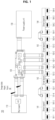
- FIG. 1 is a detailed circuit diagram of an image processing device according to one aspect of the present disclosure. Hereinafter, a configuration of an image processing device according to one aspect of the present disclosure will be described with reference to FIG. 1 .
- An image processing device 100 may include a main board 110, a timing controller board 120, a power supply unit 130, and driver boards 141, 142, 143, and 144.
- main board 110 and the timing controller board 120 are exemplified for convenience of explanation, which is also applicable to any type of display modules related to display control.
- the main board 110 described in the present specification corresponds to a first display module for example
- the timing controller board 120 corresponds to a second display module
- the scope of a right of the present disclosure should be determined according to the matters described in the claims, which is apparent to those skilled in the art.
- the main board 110 may process image data input to the image processing device 100 according to various image processing processes, and output the processed image data to the timing controller board 120.
- the types of the image processing process performed in the main board 110 are non-limited, and for example, may include demultiplexing of dividing an input transmission stream into sub-streams of an image signal, an audio signal, and additional data, decoding of an image signal, scaling of adjusting an image signal to a preset resolution, noise reduction for improving image quality, detail enhancement, frame refresh rate conversion, and the like.
- the main board 110 may perform various processes according to types and characteristics of data.
- the timing controller board 120 adjusts the amount of data transmitted to the driver boards 141, 142, 143, and 144, and controls the driver chips constituting the driver boards 141, 142, 143, and 144, respectively.
- the timing controller board 120 transmits the image data received from the main board 110 to the driver chip of each of the driver boards 141, 142, 143, and 144.
- the timing controller board 120 controls the driver boards 141, 142, 143, and 144 to adjust the timing of applying the image data for each channel of a display panel (not shown).
- the timing controller board 120 generates a control signal for controlling the driver board by receiving not only image data but also various timing signals including a vertical synchronization signal Vsync, a horizontal synchronization signal Hsync, and a Data Enable (DE) signal.
- Vsync vertical synchronization signal
- Hsync horizontal synchronization signal
- DE Data Enable
- the power supply unit 130 supplies power to the timing controller board 120.
- the power supply unit 130 may supply power to other components as needed.
- the driver boards 141, 142, 143, and 144 are disposed along the edges of the display panel to implement an image on the display panel by applying driving signals in pixel units to the display panel.
- FIG. 1 illustrates that the driver boards include four boards 141, 142, 143, and 144, the present disclosure is non-limited thereto.
- the driver boards may include a single board only or more or less than four boards.
- driver chips 141-1 to 141-4, 142-1 to 142-4, 143-1 to 143-4, or 144-1 to 144-4 are illustrated as provided to each board, but fewer or more driver chips may be provided thereto.
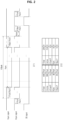
- FIG. 2 illustrates display timing according to Ultra High Definition (UHD) resolution.
- UHD Ultra High Definition
- Vsync signal vertical synchronization signal
- Hsync signal horizontal synchronization signal
- DE signal data enable signal
- the vertical synchronization signal includes a vertical synchronization period Vsync of a low logic, a vertical front porch period V Front Porch before the vertical synchronization period Vsync, and a vertical back porch period V Back Porch after the vertical synchronization period Vsync.
- the vertical synchronization period Vsync, the vertical front porch period V Front Porch, and the vertical back porch period V Back Porch may be defined as a vertical blanking period Vblank.
- the horizontal synchronization signal (Hsync signal) includes a horizontal synchronization period Hsync of the low logic and a horizontal front porch period H Front Porch before and after the horizontal synchronization period Hsync, and a horizontal back porch period H Back Porch after the horizontal synchronization period Hsync.
- the horizontal synchronization period Hsync, the horizontal front porch period H Front Porch, and the horizontal back porch period V Back Porch may be defined as a horizontal blanking period Hblank.
- the data enable signal DE becomes a high logic in a period failing to belong to any one of the vertical blanking period Vblank and the horizontal blanking period Hblank, and becomes a low logic in a period n belonging to any one of the vertical blanking period Vblank and the horizontal blanking period Hblank.
- the data enable signal (DE signal) is synchronized with the inputted image data so that the image data is displayed in a prescribed active area.
- a control (CTL) field frame may be transmitted during the vertical synchronization period Vsync.
- a signal for identifying the start and transmission of data transmission, a signal for controlling a transmission speed, a signal for detecting an error in data transmission, and the like may be transmitted through the control field frame.
- the transmission timing of the control field frame will be described in more detail later with reference to FIG. 3 .
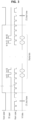
- FIG. 3 shows the transmission timing of the control field frame according to the V-by-One (Vx1) standard.
- the control field frame may be transmitted when the vertical synchronization signal (Vsync signal), the horizontal synchronization signal (Hsync signal), and the data enable signal (DE signal) all have the low logic.
- the control field frame may be transmitted when the vertical synchronization signal (Vsync signal) and the horizontal synchronization signal (Hsync signal) have the low logic and the data enable signal (DE signal) has the high logic.
- an Average Picture Level (APL) of image data may be transmitted through the control field frame.
- the APL is an average screen level, and when a 10-bit image is described as an example, black becomes 0 and full white becomes 1023, which means an average value of image data of all pixels in one frame.
- the APL may be particularly useful in power control of an Organic Light Emitting Diode (OLED) type display that uses an element capable of spontaneous emission without a separate backlight.
- OLED Organic Light Emitting Diode
- FIG. 4 and FIG. 5 show a relationship between APL and display brightness.
- images with different APLs may be displayed with different display brightness to increase expressive power or vitality.
- a first image A having a low APL may be controlled to be displayed with high display brightness. This is to allow a fine bright and dark difference in a dark image to be expressed more sensibly.
- a second image B having a high APL may be controlled to be displayed with low display brightness. This is to prevent a bright image from being displayed by being saturated.
- a frame memory (e.g., a volatile memory) for temporarily storing an image received from the image processing device may be separately provided in the display device (not shown), an APL of the image stored in the frame memory may be calculated, and then the image stored in the frame memory may be displayed on the display device according to the calculated APL.
- a separate frame memory since a separate frame memory is required to be provided in the display device, this may increase the manufacturing cost of the display device.
- the image processing device 100 can obtain an APL of the image data in advance, when the image data is processed and transmitted to the display device, the APL is transmitted together.
- the APL may be received by the image processing device 100 from an image data source (e.g., an RF antenna, a set-top box, an image player, etc.).
- APL data is transmitted together through the control field frame when image data is transmitted according to the Vx1 (V-by-One) standard.
- FIG. 6 is a diagram illustrating a specific period for generating APL data and a specific timing point of transmitting APL data according to one embodiment of the present disclosure.
- Control (CTL) data is to be transmitted once for a random period, but there is a problem that a transmission timing point is not clearly determined.
- CTL Control
- APL APL value loaded on the CTL data
- APL values are loaded on a plurality of CTL data in a specific period per frame and transmitted, and an APL value with most numerous equivalence is designed to be restored.
- Such a technology may also be referred to as Numerous Equivalence CTL reception/recovery technology.
- CTL data for example, a specific APL value
- CTL data e.g., a specific APL value
- accumulated CTL data (e.g., a plurality of e APL values) 610 and 620 are generated in a table format.
- FIG. 7 is a diagram illustrating a problem in case of transmitting APL data according to the related art.
- APL restoration data For example, if an APL value of a count '2' 710 is transmitted as '0', a receiving device (or panel, board, etc.) directly applies the APL value as "0" as it is. Therefore, an error occurs in APL restoration data according to the data error occurrence.
- the receiving device (or panel, board, etc.) directly applies the APL value as "0" as it is. Therefore, an error occurs in the APL restoration data according to the data error occurrence.
- the receiving device (or panel, board, etc.) directly applies the APL value as "0" as it is. Therefore, an error occurs in the APL restoration data according to the data error occurrence.
- the receiving device (or panel, board, etc.) directly applies the APL value as "400" as it is. Therefore, an error occurs in the APL restoration data according to the data error occurrence.
- the receiving device (or panel, board, etc.) directly applies the APL value to "300" as it is. Therefore, an error occurs in the APL restoration data according to the data error occurrence.
- the receiving device (or a panel, a board, etc.) directly applies the APL value as 512 as it is. Therefore, an error occurs in the APL restoration data according to the data error occurrence.
- the receiving device (or a panel, a board, etc.) directly applies the APL value as "512" as it is. Therefore, an error occurs in the APL restoration data according to the data error occurrence.
- FIG. 8 is a diagram illustrating a technical effect when APL data is transmitted according to an embodiment of the present disclosure.
- a plurality of APL values are designed to be loaded on CTL data and transmitted during a vertical blank period. Moreover, it is designed to finally apply an APL value with most numerous equivalence among a plurality of APL values.
- a plurality of APL values may be transmitted during a vertical blank period in one frame, and an average value 810 may be determined as a final APL value.
- an average value 810 may be determined as a final APL value.
- the possibility of error may be drastically reduced compared to the aforementioned related art shown in FIG. 7 .
- a plurality of APL values may be transmitted during a vertical blank period in one frame, and the most numerous APL value 820 may be determined as a final APL value.
- the most numerous APL value 820 may be determined as a final APL value.
- FIG. 9 is a flowchart illustrating a process for transmitting APL data by a main board and receiving it by a T-CON board according to an embodiment of the present disclosure.
- Both a main board and a timing controller (T-CON) board illustrated in FIG. 9 may be included in a display device. According to one embodiment of the present disclosure, the operation and order of each subject are defined in more detail.
- the main board generates a plurality of Average Picture Level (APL) data for each specific period within a vertical blank period (S910).
- APL Average Picture Level
- the main board transmits a plurality of the APL data to the timing controller board at a specific timing point (S920).
- the timing controller (T-CON) board receives a plurality of the APL data described above from the main board (S930).
- timing controller (T-CON) board is designed to process image data based on a specific APL data among a plurality of the received APL data (S940).
- the specific period described in the step S910 includes, for example, a case of satisfying all of a first condition in which a vertical synchronization signal Vsync is in a low state, a second condition in which a horizontal synchronization signal Hsync is in a low state, and a third condition in which a data enable signal DE is in a low state.
- the specific timing point described in the step S920 is, for example, a timing point at which the vertical synchronization signal Vsync. rises.
- the transmitting step S920 may be designed to increase data transmission efficiency by transmitting a plurality of the APL data once in a table format.
- the processing step S940 further includes comparing a plurality of the received APL data and selecting a specific APL data having most numerous equivalence.
- the same description may be repeated by those skilled in the art even if the same description is omitted.
- Vx1 V-by-One
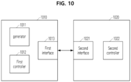
- FIG. 10 is a block diagram schematically showing a main board and a T-CON board according to one embodiment of the present disclosure.
- the present disclosure may be implemented in a display device including both of the main board and the T-CON board shown in FIG. 9 , but may also be implemented in each of the main board and the T-CON board.
- a main board 1010 for processing image data includes a generator 1011, a first controller 1012, and a first interface 1013.
- a generator 1011 a first controller 1012
- a first interface 1013 a first interface 1013.
- Each of the components may be implemented in software, hardware, or circuitry.
- the first interface 1013 performs a function for connecting to the timing controller board 1020.
- the generator 1011 generates a plurality of Average Picture Level (APL) data for each specific period within a vertical blank period.
- APL Average Picture Level
- the first controller 1012 controls the first interface 1013 to transmit a plurality of the APL data to the timing controller board 1020 at a specific timing point.
- the specific period is designed to include, for example, a first condition in which a vertical synchronization signal Vsync is in a low state, a second condition in which a horizontal synchronization signal Hsync is in a low state, and a third condition in which a data enable signal DE is in a low state.
- the specific timing point is, for example, a timing point at which the vertical synchronization signal Vsync rises.
- the first controller 1012 is characterized in controlling the interface to transmit a plurality of the APL data once in a table format, for example.
- a timing controller board 1020 for processing image data includes a second controller 1022 and a second interface 1021.
- Each of the components may be implemented in software, hardware or circuit.
- the second interface 1021 receives a plurality of the APL data from the main board 1010.
- the second controller 1022 processes image data based on a specific APL data among a plurality of the received APL data.
- the second controller 1022 is characterized in comparing a plurality of the received APL data and selecting a specific APL data with the most numerous equivalence.
- FIG. 8 (b) even if the same description is omitted, it is possible for those skilled in the art to repeatedly embody it.
- a plurality of the APL data are characterized in being generated by the main board 1010 when the first condition in which the vertical synchronization signal Vsync is in the low state, the second condition in which the horizontal synchronization signal Hsync is in the low state, and the third condition in which the data enable signal DE is in the low state are satisfied within the vertical blank period.
- an image processing device may be implemented in the form of an IC for each component or a combination of two or more components, and the function of the image processing device may be implemented in the form of a program and installed on the IC.
- the function of the image processing device according to the present disclosure is implemented as a program
- the function of each component included in the image processing device may be implemented as a specific code, and codes for implementing a specific function may be implemented as one program or may be implemented by being divided into a plurality of programs.
Landscapes
- Engineering & Computer Science (AREA)
- Physics & Mathematics (AREA)
- Computer Hardware Design (AREA)
- General Physics & Mathematics (AREA)
- Theoretical Computer Science (AREA)
- Control Of Indicators Other Than Cathode Ray Tubes (AREA)
Applications Claiming Priority (2)
| Application Number | Priority Date | Filing Date | Title |
|---|---|---|---|
| KR20230011395 | 2023-01-30 | ||
| KR1020230129111A KR20240119808A (ko) | 2023-01-30 | 2023-09-26 | 디스플레이 장치 및 제어 방법 |
Publications (1)
| Publication Number | Publication Date |
|---|---|
| EP4407597A1 true EP4407597A1 (de) | 2024-07-31 |
Family
ID=89715817
Family Applications (1)
| Application Number | Title | Priority Date | Filing Date |
|---|---|---|---|
| EP24153597.0A Pending EP4407597A1 (de) | 2023-01-30 | 2024-01-24 | Anzeigevorrichtung und verfahren zur steuerung davon |
Country Status (2)
| Country | Link |
|---|---|
| US (1) | US12293696B2 (de) |
| EP (1) | EP4407597A1 (de) |
Citations (4)
| Publication number | Priority date | Publication date | Assignee | Title |
|---|---|---|---|---|
| US20020136241A1 (en) * | 2001-01-24 | 2002-09-26 | Christopher Pasqualino | Digital visual interface with audio and auxiliary data |
| WO2006095313A1 (en) * | 2005-03-11 | 2006-09-14 | Koninklijke Philips Electronics N.V. | Method for remotely controlling a display apparatus based thereon and a portable device comprising such an apparatus |
| US20150062186A1 (en) * | 2013-09-02 | 2015-03-05 | Sungjin Park | Display device and luminance control method thereof |
| KR20230011395A (ko) | 2021-06-10 | 2023-01-20 | 텐센트 아메리카 엘엘씨 | 제로 잔차 플래그 코딩 |
Family Cites Families (1)
| Publication number | Priority date | Publication date | Assignee | Title |
|---|---|---|---|---|
| JP6598430B2 (ja) * | 2013-10-31 | 2019-10-30 | キヤノン株式会社 | 表示装置、表示装置の制御方法、及び、プログラム |
-
2024
- 2024-01-24 EP EP24153597.0A patent/EP4407597A1/de active Pending
- 2024-01-29 US US18/425,650 patent/US12293696B2/en active Active
Patent Citations (4)
| Publication number | Priority date | Publication date | Assignee | Title |
|---|---|---|---|---|
| US20020136241A1 (en) * | 2001-01-24 | 2002-09-26 | Christopher Pasqualino | Digital visual interface with audio and auxiliary data |
| WO2006095313A1 (en) * | 2005-03-11 | 2006-09-14 | Koninklijke Philips Electronics N.V. | Method for remotely controlling a display apparatus based thereon and a portable device comprising such an apparatus |
| US20150062186A1 (en) * | 2013-09-02 | 2015-03-05 | Sungjin Park | Display device and luminance control method thereof |
| KR20230011395A (ko) | 2021-06-10 | 2023-01-20 | 텐센트 아메리카 엘엘씨 | 제로 잔차 플래그 코딩 |
Also Published As
| Publication number | Publication date |
|---|---|
| US12293696B2 (en) | 2025-05-06 |
| US20240257701A1 (en) | 2024-08-01 |
Similar Documents
| Publication | Publication Date | Title |
|---|---|---|
| US10038904B2 (en) | Method and apparatus for controlling transmission of compressed picture according to transmission synchronization events | |
| US8266335B2 (en) | Video display device, method of displaying connectors, transmission-line state detection device, transmission line-state detection method and semiconductor integrated circuit | |
| JP5857588B2 (ja) | 送信装置、送信方法、受信装置、受信方法および送受信システム | |
| AU2014339383A1 (en) | Method and apparatus for controlling transmission of compressed picture according to transmission synchronization events | |
| US20110157198A1 (en) | Techniques for aligning frame data | |
| US7880713B2 (en) | Method of increasing efficiency of video display and related apparatus | |
| CN102456328B (zh) | 液晶显示装置及其驱动方法、液晶电视 | |
| CN106847209B (zh) | 一种显示驱动方法、显示驱动装置以及显示装置 | |
| US10440424B2 (en) | Transmission apparatus, transmission method, reception apparatus, and reception method | |
| EP1983756A1 (de) | Tragbare Vorrichtung mit Videoausgabe | |
| CN113299251A (zh) | 一种处理器的控制方法及处理器 | |
| WO2020207144A1 (zh) | 一种显示装置、图像显示方法和电子设备 | |
| CN111292668A (zh) | 显示面板的刷新频率调整方法及装置 | |
| WO2016047030A1 (ja) | 表示装置及び表示方法 | |
| JP2013097379A (ja) | ビデオフォーマット変換を有するタイミング制御部、その方法、並びにディスプレイシステム | |
| US10515578B2 (en) | Electrical circuit and display apparatus | |
| KR20240119808A (ko) | 디스플레이 장치 및 제어 방법 | |
| CN105304053B (zh) | 时序控制芯片内起始信号控制方法、芯片及显示面板 | |
| CN101911669B (zh) | 同步信号转换电路和具有该电路的信号处理系统、以及同步信号转换方法 | |
| CN107978285B (zh) | 用于响应显示数据而驱动显示面板的装置和方法 | |
| US20130271650A1 (en) | Video display apparatus and video processing method | |
| US12293696B2 (en) | Display device and method of controlling the same | |
| US20140098849A1 (en) | Method and device for creating and maintaining synchronization between video signals | |
| KR20130093432A (ko) | 구동 장치, 이를 포함하는 표시 장치 및 그 구동 방법 | |
| US8379149B2 (en) | Display apparatus and control method thereof |
Legal Events
| Date | Code | Title | Description |
|---|---|---|---|
| PUAI | Public reference made under article 153(3) epc to a published international application that has entered the european phase |
Free format text: ORIGINAL CODE: 0009012 |
|
| STAA | Information on the status of an ep patent application or granted ep patent |
Free format text: STATUS: THE APPLICATION HAS BEEN PUBLISHED |
|
| AK | Designated contracting states |
Kind code of ref document: A1 Designated state(s): AL AT BE BG CH CY CZ DE DK EE ES FI FR GB GR HR HU IE IS IT LI LT LU LV MC ME MK MT NL NO PL PT RO RS SE SI SK SM TR |
|
| STAA | Information on the status of an ep patent application or granted ep patent |
Free format text: STATUS: REQUEST FOR EXAMINATION WAS MADE |
|
| 17P | Request for examination filed |
Effective date: 20250129 |
|
| P01 | Opt-out of the competence of the unified patent court (upc) registered |
Free format text: CASE NUMBER: APP_5209/2025 Effective date: 20250131 |
|
| STAA | Information on the status of an ep patent application or granted ep patent |
Free format text: STATUS: EXAMINATION IS IN PROGRESS |