EP4407327A1 - Effektive scan-abdeckung - Google Patents
Effektive scan-abdeckung Download PDFInfo
- Publication number
- EP4407327A1 EP4407327A1 EP24150870.4A EP24150870A EP4407327A1 EP 4407327 A1 EP4407327 A1 EP 4407327A1 EP 24150870 A EP24150870 A EP 24150870A EP 4407327 A1 EP4407327 A1 EP 4407327A1
- Authority
- EP
- European Patent Office
- Prior art keywords
- flop
- flip
- digital circuit
- output
- circuit
- Prior art date
- Legal status (The legal status is an assumption and is not a legal conclusion. Google has not performed a legal analysis and makes no representation as to the accuracy of the status listed.)
- Withdrawn
Links
Images


Classifications
-
- G—PHYSICS
- G01—MEASURING; TESTING
- G01R—MEASURING ELECTRIC VARIABLES; MEASURING MAGNETIC VARIABLES
- G01R31/00—Arrangements for testing electric properties; Arrangements for locating electric faults; Arrangements for electrical testing characterised by what is being tested not provided for elsewhere
- G01R31/28—Testing of electronic circuits, e.g. by signal tracer
- G01R31/317—Testing of digital circuits
- G01R31/31702—Testing digital circuits including elements other than semiconductor transistors, e.g. biochips, nanofabrics, mems, chips with magnetic elements
-
- G—PHYSICS
- G01—MEASURING; TESTING
- G01R—MEASURING ELECTRIC VARIABLES; MEASURING MAGNETIC VARIABLES
- G01R31/00—Arrangements for testing electric properties; Arrangements for locating electric faults; Arrangements for electrical testing characterised by what is being tested not provided for elsewhere
- G01R31/28—Testing of electronic circuits, e.g. by signal tracer
- G01R31/317—Testing of digital circuits
- G01R31/3181—Functional testing
- G01R31/3185—Reconfiguring for testing, e.g. LSSD, partitioning
- G01R31/318533—Reconfiguring for testing, e.g. LSSD, partitioning using scanning techniques, e.g. LSSD, Boundary Scan, JTAG
- G01R31/318544—Scanning methods, algorithms and patterns
-
- G—PHYSICS
- G01—MEASURING; TESTING
- G01R—MEASURING ELECTRIC VARIABLES; MEASURING MAGNETIC VARIABLES
- G01R31/00—Arrangements for testing electric properties; Arrangements for locating electric faults; Arrangements for electrical testing characterised by what is being tested not provided for elsewhere
- G01R31/28—Testing of electronic circuits, e.g. by signal tracer
- G01R31/317—Testing of digital circuits
- G01R31/31704—Design for test; Design verification
-
- G—PHYSICS
- G01—MEASURING; TESTING
- G01R—MEASURING ELECTRIC VARIABLES; MEASURING MAGNETIC VARIABLES
- G01R31/00—Arrangements for testing electric properties; Arrangements for locating electric faults; Arrangements for electrical testing characterised by what is being tested not provided for elsewhere
- G01R31/28—Testing of electronic circuits, e.g. by signal tracer
- G01R31/317—Testing of digital circuits
- G01R31/31724—Test controller, e.g. BIST state machine
-
- G—PHYSICS
- G01—MEASURING; TESTING
- G01R—MEASURING ELECTRIC VARIABLES; MEASURING MAGNETIC VARIABLES
- G01R31/00—Arrangements for testing electric properties; Arrangements for locating electric faults; Arrangements for electrical testing characterised by what is being tested not provided for elsewhere
- G01R31/28—Testing of electronic circuits, e.g. by signal tracer
- G01R31/317—Testing of digital circuits
- G01R31/3181—Functional testing
- G01R31/31813—Test pattern generators
-
- G—PHYSICS
- G01—MEASURING; TESTING
- G01R—MEASURING ELECTRIC VARIABLES; MEASURING MAGNETIC VARIABLES
- G01R31/00—Arrangements for testing electric properties; Arrangements for locating electric faults; Arrangements for electrical testing characterised by what is being tested not provided for elsewhere
- G01R31/28—Testing of electronic circuits, e.g. by signal tracer
- G01R31/317—Testing of digital circuits
- G01R31/3181—Functional testing
- G01R31/3183—Generation of test inputs, e.g. test vectors, patterns or sequences
- G01R31/318364—Generation of test inputs, e.g. test vectors, patterns or sequences as a result of hardware simulation, e.g. in an HDL environment
-
- G—PHYSICS
- G01—MEASURING; TESTING
- G01R—MEASURING ELECTRIC VARIABLES; MEASURING MAGNETIC VARIABLES
- G01R31/00—Arrangements for testing electric properties; Arrangements for locating electric faults; Arrangements for electrical testing characterised by what is being tested not provided for elsewhere
- G01R31/28—Testing of electronic circuits, e.g. by signal tracer
- G01R31/317—Testing of digital circuits
- G01R31/3181—Functional testing
- G01R31/3183—Generation of test inputs, e.g. test vectors, patterns or sequences
- G01R31/318392—Generation of test inputs, e.g. test vectors, patterns or sequences for sequential circuits
-
- G—PHYSICS
- G01—MEASURING; TESTING
- G01R—MEASURING ELECTRIC VARIABLES; MEASURING MAGNETIC VARIABLES
- G01R31/00—Arrangements for testing electric properties; Arrangements for locating electric faults; Arrangements for electrical testing characterised by what is being tested not provided for elsewhere
- G01R31/28—Testing of electronic circuits, e.g. by signal tracer
- G01R31/317—Testing of digital circuits
- G01R31/3181—Functional testing
- G01R31/3185—Reconfiguring for testing, e.g. LSSD, partitioning
- G01R31/318533—Reconfiguring for testing, e.g. LSSD, partitioning using scanning techniques, e.g. LSSD, Boundary Scan, JTAG
- G01R31/318536—Scan chain arrangements, e.g. connections, test bus, analog signals
-
- G—PHYSICS
- G01—MEASURING; TESTING
- G01R—MEASURING ELECTRIC VARIABLES; MEASURING MAGNETIC VARIABLES
- G01R31/00—Arrangements for testing electric properties; Arrangements for locating electric faults; Arrangements for electrical testing characterised by what is being tested not provided for elsewhere
- G01R31/28—Testing of electronic circuits, e.g. by signal tracer
- G01R31/317—Testing of digital circuits
- G01R31/3181—Functional testing
- G01R31/3185—Reconfiguring for testing, e.g. LSSD, partitioning
- G01R31/318533—Reconfiguring for testing, e.g. LSSD, partitioning using scanning techniques, e.g. LSSD, Boundary Scan, JTAG
- G01R31/318541—Scan latches or cell details
-
- G—PHYSICS
- G01—MEASURING; TESTING
- G01R—MEASURING ELECTRIC VARIABLES; MEASURING MAGNETIC VARIABLES
- G01R31/00—Arrangements for testing electric properties; Arrangements for locating electric faults; Arrangements for electrical testing characterised by what is being tested not provided for elsewhere
- G01R31/28—Testing of electronic circuits, e.g. by signal tracer
- G01R31/317—Testing of digital circuits
- G01R31/3181—Functional testing
- G01R31/3185—Reconfiguring for testing, e.g. LSSD, partitioning
- G01R31/318533—Reconfiguring for testing, e.g. LSSD, partitioning using scanning techniques, e.g. LSSD, Boundary Scan, JTAG
- G01R31/318597—JTAG or boundary scan test of memory devices
-
- G—PHYSICS
- G01—MEASURING; TESTING
- G01R—MEASURING ELECTRIC VARIABLES; MEASURING MAGNETIC VARIABLES
- G01R31/00—Arrangements for testing electric properties; Arrangements for locating electric faults; Arrangements for electrical testing characterised by what is being tested not provided for elsewhere
- G01R31/28—Testing of electronic circuits, e.g. by signal tracer
- G01R31/317—Testing of digital circuits
- G01R31/3181—Functional testing
- G01R31/3187—Built-in tests
-
- G—PHYSICS
- G01—MEASURING; TESTING
- G01R—MEASURING ELECTRIC VARIABLES; MEASURING MAGNETIC VARIABLES
- G01R31/00—Arrangements for testing electric properties; Arrangements for locating electric faults; Arrangements for electrical testing characterised by what is being tested not provided for elsewhere
- G01R31/28—Testing of electronic circuits, e.g. by signal tracer
- G01R31/317—Testing of digital circuits
- G01R31/3181—Functional testing
- G01R31/319—Tester hardware, i.e. output processing circuits
- G01R31/31903—Tester hardware, i.e. output processing circuits tester configuration
- G01R31/31905—Interface with the device under test [DUT], e.g. arrangements between the test head and the DUT, mechanical aspects, fixture
-
- G—PHYSICS
- G01—MEASURING; TESTING
- G01R—MEASURING ELECTRIC VARIABLES; MEASURING MAGNETIC VARIABLES
- G01R31/00—Arrangements for testing electric properties; Arrangements for locating electric faults; Arrangements for electrical testing characterised by what is being tested not provided for elsewhere
- G01R31/28—Testing of electronic circuits, e.g. by signal tracer
- G01R31/317—Testing of digital circuits
- G01R31/3181—Functional testing
- G01R31/319—Tester hardware, i.e. output processing circuits
- G01R31/31903—Tester hardware, i.e. output processing circuits tester configuration
- G01R31/31907—Modular tester, e.g. controlling and coordinating instruments in a bus based architecture
-
- G—PHYSICS
- G01—MEASURING; TESTING
- G01R—MEASURING ELECTRIC VARIABLES; MEASURING MAGNETIC VARIABLES
- G01R31/00—Arrangements for testing electric properties; Arrangements for locating electric faults; Arrangements for electrical testing characterised by what is being tested not provided for elsewhere
- G01R31/28—Testing of electronic circuits, e.g. by signal tracer
- G01R31/317—Testing of digital circuits
- G01R31/3181—Functional testing
- G01R31/319—Tester hardware, i.e. output processing circuits
- G01R31/31903—Tester hardware, i.e. output processing circuits tester configuration
- G01R31/31908—Tester set-up, e.g. configuring the tester to the device under test [DUT], down loading test patterns
Definitions
- the present disclosure generally relates to digital logic.
- one or more embodiments relate to an improved area, cost, and time-effective scan coverage as applied to digital logic.
- DFT design for testability
- ATG automatic test pattern generation
- LBIST logic built-in self-test
- ATPG is a computer-aided design (CAD) technique that automatically generates test patterns for a digital circuit.
- the randomly generated test patterns are used to verify the proper functioning and identify defects or faults in the digital circuit.
- ATPG uses external test equipment to verify the correct fabrication of the circuit.
- LBIST uses built-in circuits to perform tests on the digital circuit. With LBIST, test patterns are generated and applied within the circuit (that is, no external test equipment is needed). The test results are then compared to the expected results to determine the proper functioning of the circuit.
- LBIST can test the circuit's functionality at various stages of its operation, including during power-up, normal operation, or low-power mode.
- Scan-design is commonly used to test an internal circuit under test (CUT).
- the external input/output (I/O) of the larger circuit-to which the CUT belongs- is used to deliver test data and observe the corresponding test outputs.
- Various flip-flops of the circuit are connected to one or more scan chains, and test patterns are shifted from the I/O pins through the scan chains. The test results are shifted out to the I/O pins and compared to an expected result to determine circuit defects.
- the conventional scan-design techniques fail to test for all points in the circuit, and some functional combination logic circuits are not covered during the test (that is, less than 100 % coverage).
- a first aspect relates to a digital circuit.
- the digital circuit includes an OR gate and a flip-flop.
- the OR gate includes a first input and a second input.
- the first input of the OR gate is coupled to a control signal, and the second input of the OR gate is coupled to an uncovered functional combination logic of the digital circuit.
- the first input of the OR gate is configured to be pulled low by the control signal in response to setting the digital circuit in a configuration to test the uncovered functional combination logic.
- the flip-flop includes a reset pin or a set pin coupled to the output of the OR gate.
- the output of the flip-flop is configured to be observed during a testing of the uncovered functional combination logic to detect defects in the digital circuit.
- a last scan shift value of the flip-flop is overridden, and a stuck-at "1" fault condition is observed for the uncovered functional combination logic at the output of the flip-flop.
- the flip-flop is a boundary scan flip-flop or a control flip-flop of the digital circuit.
- the flip-flop is a resettable functional flip-flop of the digital circuit.
- the digital circuit further includes a multiplexer, a one-hot decoder circuit, a second flip-flop, and a second OR gate.
- the multiplexer includes a first input and a second input.
- the first input is coupled to a pad of the digital circuit, and the second input is coupled to an LBIST control signal.
- An output of the multiplexer is coupled to the LBIST control signal during LBIST in response to setting the digital circuit in the configuration to test the uncovered functional combination logic.
- the output of the multiplexer is coupled to a pad of the digital circuit during ATPG functions.
- the one-hot decoder circuit is configured to generate a first clock signal and second clock signals provided to the rest of the digital circuit.
- the second flip-flop includes a clock input, a data input, and an output.
- the clock input is coupled to the output of the one-hot decoder circuit and configured to receive the first clock signal.
- the data input is coupled to the output of the multiplexer.
- the second flip-flop includes a clock input, a data input, and an output.
- the clock input of the second flip-flop is coupled to the output of the one-hot decoder circuit, and the data input of the second flip-flop is coupled to the output of the multiplexer.
- the second OR gate is coupled to the output of the second flip-flop.
- the second OR gate is configured to generate the control signal in response to setting the digital circuit in the configuration to test the uncovered functional combination logic.
- the digital circuit further includes a multiplexer arranged between the output of the OR gate and the reset pin or the set pin of the flip-flop.
- the multiplexer is configured to couple the OR gate to the flip-flop in response to setting the digital circuit in the configuration to test the uncovered functional combination logic.
- a second aspect relates to a digital circuit.
- the digital circuit includes an XOR tree, a plurality of OR gates, and a plurality of boundary scan flip-flops.
- the XOR tree includes a plurality of inputs; each input coupled to an associated uncovered functional combination logic.
- Each OR gate has a first input coupled to a control signal and a second input coupled to an associated output of the XOR tree. The control signal is pulled low in response to setting the digital circuit in a configuration to test the associated uncovered functional combination logic.
- Each boundary scan flip-flop has a reset pin or a set pin coupled to an associated OR gate. The output of each boundary scan flip-flop is configured to be observed during testing the associated uncovered functional combination logic to detect defects in the digital circuit.
- each input of the XOR tree is coupled to the associated uncovered functional combination logic of the digital circuit at a periphery of the digital circuit.
- the digital circuit further includes a multiplexer, a one-hot decoder circuit, a second flip-flop, and a control OR gate.
- the multiplexer includes a first input and a second input.
- the first input is coupled to a pad of the digital circuit, and the second input is coupled to an LBIST control signal.
- An output of the multiplexer is coupled to the LBIST control signal during LBIST in response to setting the digital circuit in the configuration to test the uncovered functional combination logic.
- the output of the multiplexer is coupled to a pad of the digital circuit during ATPG functions.
- the one-hot decoder circuit is configured to generate a first clock signal and second clock signals provided to the rest of the digital circuit.
- the second flip-flop includes a clock input, a data input, and an output.
- the clock input is coupled to the output of the one-hot decoder circuit and configured to receive the first clock signal.
- the data input is coupled to the output of the multiplexer.
- the control OR gate is coupled to the output of the second flip-flop and is configured to generate the control signal in response to setting the digital circuit in the configuration to test the associated uncovered functional combination logic.
- a third implementation form of the digital circuit according to the second aspect as such or any preceding implementation form of the second aspect in response to the reset pin or the set pin being pulled high during the testing of the associated uncovered functional combination logic, a last scan shift value of a respective boundary scan flip-flop is overridden, and a stuck-at "1" fault condition is observed for the associated uncovered functional combination logic at the output of the respective boundary scan flip-flop.
- a fourth implementation form of the digital circuit according to the second aspect as such or any preceding implementation form of the second aspect in response to the reset pin or the set pin remaining low during the testing of the associated uncovered functional combination logic, a last scan shift value of the respective boundary scan flip-flop is retained, and a stuck-at "0" fault condition is observed for the associated uncovered functional combination logic at the output of the respective boundary scan flip-flop.
- the digital circuit further includes a plurality of multiplexers arranged between the output of each OR gate and the reset pin or the set pin of the respective boundary scan flip-flop.
- a respective multiplexer is configured to couple each OR gate to the respective boundary scan flip-flop in response to setting the digital circuit in the configuration to test the associated uncovered functional combination logic.
- the digital circuit further includes a control flip-flop configured to test an associated uncovered functional combination logic of the digital circuit coupled to a digital input of an analog IP using a scan chain.
- a third aspect relates to a digital circuit.
- the digital circuit includes a multiplexer, an OR gate, a first functional combination logic circuit, a second functional combination logic circuit and a control flip-flop.
- the OR gate includes a first input coupled to a control signal.
- the first functional combination logic circuit is coupled to a first input of the multiplexer and a second input of the OR gate.
- the control signal is pulled low in response to setting the digital circuit in a configuration to test the first functional combination logic circuit.
- the second functional combination logic circuit is coupled to the output of the multiplexer, and the second functional combination logic circuit is configured to receive the output of the first functional combination logic circuit during a functional mode operation or an analog IP test mode operation of the digital circuit, and receive a tied safe state value during a scan mode of the digital circuit to keep the analog IP in a power down state.
- the control flip-flop includes a reset pin or a set pin coupled to the output of the OR gate. The control flip-flop is configured to be observed during the testing of the first functional combination logic circuit to detect defects in the digital circuit.
- the digital circuit further includes a second multiplexer having a first input coupled to the digital output of the second functional combination logic circuit and a second input coupled to the output of the control flip-flop.
- the second functional combination logic circuit is an analog IP
- the first functional combination logic circuit drives the digital input of analog IP
- the analog IP is one of an analog to digital converter, a power management block, a flash, a fuse, a clock source, a threshold detector, or a process monitor.
- the digital circuit in response to the reset pin or the set pin being pulled high during the testing of the first functional combination logic circuit, the digital circuit is configured to override a last scan shift value of the control flip-flop, and observe a stuck-at "1" fault condition for the first functional combination logic circuit at the output of the control flip-flop. In response to the reset pin or the set pin remaining low during the testing of the first functional combination logic circuit, the digital circuit is configured to retain a last scan shift value of the control flip-flop, and observe a stuck-at "0" fault condition for the first functional combination logic circuit at the output of the control flip-flop.
- the digital circuit further includes a second multiplexer, a one-hot decoder circuit, a second flip-flop, and a control OR gate.
- the second multiplexer includes a first input and a second input.
- the first input is coupled to a pad of the digital circuit, and the second input is coupled to an LBIST control signal.
- An output of the second multiplexer is coupled to the LBIST control signal during LBIST in response to setting the digital circuit in the configuration to test the uncovered functional combination logic.
- the output of the second multiplexer is coupled to a pad of the digital circuit during ATPG functions.
- the one-hot decoder circuit is configured to generate a first clock signal and second clock signals provided to the rest of the digital circuit.
- the second flip-flop includes a clock input, a data input, and an output.
- the clock input is coupled to the output of the one-hot decoder circuit and configured to receive the first clock signal.
- the data input is coupled to the output of the second multiplexer.
- the control OR gate is coupled to the output of the second flip-flop.
- the control OR gate is configured to generate the control signal in response to setting the digital circuit in the configuration to test the first functional combination logic circuit.
- Embodiments can be implemented in hardware, software, or in any combination thereof.
- a digital circuit includes an OR gate and an existing flip-flop.
- An input of the OR gate is coupled to a control signal.
- a second input of the OR gate is coupled to a functional combination logic circuit of the digital circuit not covered during the scan mode testing of the digital circuit.
- the control signal is configured to be pulled low in response to setting the digital circuit in a configuration to test the uncovered functional combination logic.
- the OR gate is coupled to a reset pin or set pin of the existing flip-flop. The output of the flip-flop is observed during the testing of the uncovered functional combination logic to detect defects in the digital circuit.
- the last scan shift value of the flip-flop in response to the reset pin or the set pin being pulled high during the testing of the uncovered functional combination logic, the last scan shift value of the flip-flop is overridden, and a stuck-at "1" fault condition is observed for the uncovered functional combination logic at the output of the flip-flop.
- the last scan shift value of the flip-flop in response to the reset pin or the set pin remaining low during the testing of the uncovered functional combination logic, the last scan shift value of the flip-flop is retained, and a stuck-at "0" fault condition is observed for the uncovered functional combination logic at the output of the flip-flop.
- the flip-flop selected during the digital circuit design is a boundary scan flip-flop when the logic to be scanned (that is, observation logic) is near an output pad of the digital circuit.
- the flip-flop selected during the digital circuit design is a control flip-flop of the digital circuit when the logic to be scanned is within the core logic of the digital circuit.
- the control circuit includes a multiplexer, a one-hot decoder circuit, a second flip-flop, and a second OR gate.
- the multiplexer includes a first input coupled to a pad of the digital circuit used as control for ATPG operations, and a second input coupled to an LBIST control signal.
- the output of the multiplexer is coupled to the LBIST control signal in response to setting the digital circuit in the configuration to test the uncovered functional combination logic.
- the output of the multiplexer is coupled to the pad of the digital circuit in all other conditions and used in ATPG operations to set the digital circuit in the configuration to test the uncovered functional combination logic.
- the one-hot decoder circuit is configured to generate a clock signal received at a clock input of the second flip-flop.
- the data input of the second flip-flop is coupled to the output of the multiplexer.
- the second OR gate is coupled to the output of the second flip-flop.
- the second OR gate is configured to generate the control signal in response to setting the digital circuit in the configuration to test the uncovered functional combination logic.
- the digital circuit includes a multiplexer arranged between the output of the OR gate and the reset pin or the set pin of the flip-flop.
- the multiplexer is configured to couple the OR gate to the flip-flop in response to setting the digital circuit in the configuration to test the uncovered functional combination logic.
- the conventional scan-design techniques fail to test for all points in the circuit.
- Various industries require a circuit with a minimum coverage target during various test modes.
- the automotive industry has a minimum stuck-at coverage target requirement of 99 % for production (i.e., ATPG) and 90 % for self-test (i.e., LBIST at customer environment).
- ATPG a minimum stuck-at coverage target requirement of 99 % for production
- self-test i.e., LBIST at customer environment
- Figure 1 illustrates a block diagram of a conventional scan flip-flop 100 of a scan chain.
- the scan flip-flop 100 includes a multiplexer (MUX) 102 coupled with a flip-flop 104.
- MUX multiplexer
- Multiple scan flip-flops are arranged in a scan chain to test one or more logic components in the digital circuit using ATPG or LBIST techniques.
- Multiplexer 102 includes a functional input, a test input, a scan/test enable input, and an output.
- the value at the scan/test enable input determines which of the functional input or test input is selected at the output of the multiplexer 102.
- the functional input is coupled to the digital circuit's uncovered functional combinational logic circuit.
- a clock signal is used to control the scan flip-flop 100 along the scan chain.
- the output of the flip-flop 104 provides the result of the test pattern for the portion of the CUT coupled to the scan flip-flop 100.
- Typical analog IP includes analog to digital converters (ADC) (e.g., successive successive-approximation ADC), power management blocks, flash, fuse, clock sources (e.g., phase-locked loop, crystal oscillators, RC oscillators), threshold detectors, process monitors, and the like.
- ADC analog to digital converters
- Figure 2 illustrates a block diagram of circuit 200, which includes a scan flip-flop 100 in combination with an observability flip-flop 202.
- Circuit 200 is a first prior art solution to test uncovered functional combinational logic.
- the uncovered functional combinational logic of the CUT is tied to the data (D) input of the observability flip-flop 202.
- D data
- the uncovered functional combinational logic is, thus, tested.
- observability flip-flop 202 is added for structural testing of the uncovered functional combinational logic and provides no other functional purposes. Adding the observability flip-flop 202 to the scan chain increases cost, circuit footprint, scan chain length, test time, and self-test time (i.e., LBIST) in the application environment.
- each observability flip-flop 202 adds an additional cycle to a scan chain.
- a typical digital circuit can include many observability flip-flops due to the many scan chains. In a scan chain that includes a hundred flip-flops, the observability flip-flop 202 adds an additional clock cycle to the test sequence. As a digital circuit may include thousands of flip-flops, adding the observability flip-flop 202 to each scan chain increases test time.
- each observability flip-flop 202 requires a clock signal for synchronicity, and corresponding patterns to meet setup and hold requirements are, thus, needed, which adds cost, time, and circuit footprint. Moreover, adding an observability flip-flop 202 along the functional path of the digital circuit adds unwanted delay time to the functional operations of the digital circuit.
- Figure 3 illustrates a block diagram of circuit 300, a second prior art solution used to test uncovered functional combination logic.
- a first uncovered functional combination logic is coupled to the data (D) pin of an existing functional flip-flop 306 through an AND gate 302 and an OR gate 304; a second uncovered functional combination logic is coupled to a second input of the OR gate 304.
- the first input to the AND gate 302 is at a logic low (i.e., "0").
- the output of the AND gate 302 and the first input to the OR gate 304 is at a logic low.
- the input to the existing functional flip-flop 306 is the second uncovered functional combination logic received at the second input of the OR gate 304.
- the functional flip-flop 306 is an existing flip-flop used in the circuit tied to the second uncovered functional combination logic.
- the first input to the AND gate 302 is at a logic high (i.e., "1").
- the first and second uncovered functional combination logic circuits can be tested.
- the LBIST controller e.g., field-programmable gate array (FPGA) sets the second uncovered functional combination logic to zero, and to test the second uncovered functional combination logic, the LBIST controller sets the first uncovered functional combination logic to zero.
- the input to the existing functional flip-flop 306 is, thus, one of the first or second uncovered functional combination logics based on the LBIST controller setting.
- circuit 300 the additional gates add unwanted delay along the high-frequency functional paths. Further, the test pattern count is increased by switching between the functional paths, which increases test time. Finally, the additional logic adds complexity, which increases costs.
- Figure 4 illustrates a block diagram of an embodiment circuit 400 for testing uncovered functional combination logic of a digital circuit.
- Circuit 400 includes the scan flip-flop 100, an OR gate 402, a multiplexer (MUX) 404, and an existing D (i.e., Data or Delay) flip-flop 406, which may (or may not) be arranged as shown. Further, circuit 400 may include additional components not shown in Figure 4 .
- MUX multiplexer
- the uncovered functional combination logic is coupled to a first input of OR gate 402.
- a control signal is received at the second input of OR gate 402-detailed further below.
- the output of OR gate 402 is coupled to the first input of multiplexer 404.
- the second input of multiplexer 404 is coupled to a reset path used to reset the existing D flip-flop 406.
- the output of the multiplexer 404 is coupled to the reset (R) pin or a set (S) pin of an existing D flip-flop 406.
- the output of multiplexer 404 can be coupled to the set (S) pin of the existing D flip-flop 406 in other embodiments.
- an optional multiplexer 404 couples the OR gate 402 to the reset (R) pin of the existing D flip-flop 406.
- the enable signal fed to the multiplexer 404 allows a selection between (i) the original reset signal during the functional mode or (ii) the original reset signal or uncovered functional combination logic in the test mode at the reset (R) pin of the existing D flip-flop 406.
- the original reset signal or uncovered functional combination logic is coupled to the reset (R) pin of the existing D flip-flop 406 based on the particular scan capture operation performed during a scan capture.
- the reset (R) pin of the existing D flip-flop 406 is coupled to the original reset path of the circuit through multiplexer 404.
- the existing D flip-flop 406 is an existing boundary scan flip-flop of the digital circuit.
- the existing D flip-flop 406 is an existing boundary scan flip-flop when the logic to be scanned (i.e., observation logic) is "near" an output pad of the digital circuit.
- the uncovered functional combination logic is "near" an existing boundary scan flip-flip when it is used to drive an enable or data pad of the digital circuit in functional mode (i.e., non-boundary scan mode).
- the distance may vary based on the functional timing requirements of the sub-circuit, such as controller area network (CAN) protocols for CAN pads, local interconnect network (LIN) protocols for LIN pads, or the like.
- CAN controller area network
- LIN local interconnect network
- a boundary scan flip-flop is a digital logic element specifically designed for boundary scan testing of the digital circuit.
- boundary scan testing a series of flip-flops are placed around the periphery of the digital circuit. The input and output of each flip-flop are, thus, accessible through a test interface.
- the boundary scan flip-flop allows the digital circuit to be tested by applying a set of test patterns to the input of the flip-flop. The resulting output patterns of the flip-flop are then observed to check for defects or faults.
- boundary scan flip-flops are used in complex or large circuits where the traditional functional test or built-in test methods are unavailable.
- boundary scan-flops are added to a digital circuit to support 1149.1 standard operations.
- the enable signals at the I/O pads are driven by the boundary scan flip-flops to configure pads as output or input
- data signals at the I/O pads are driven by the boundary scan flip-flops when the pads are configured as output and data signals at the I/O pads are observed when the pads are used as an input by the boundary scan flip-flops (e.g., during board level testing)
- Boundary scan flip-flops are available in all digital circuits for general purpose input output (GPIO) parametric and board testing (i.e., customer boards).
- GPIO general purpose input output
- the existing D flip-flop 406 is an existing control flip-flop of the digital circuit.
- the existing D flip-flop 406 is an existing control flip-flop when the functional combination logic to be scanned is within the core logic of the digital circuit.
- the functional combination logic is said to be within the core logic of the digital circuit when it is not used to drive an output pad or observe an input pad.
- the functional combination logic between two flip-flops or the functional combination logic to an analog IP or from an analog IP is within the core logic of the digital circuit.
- a control flip-flop is a configurable flip-flop added to a digital circuit to improve scan coverage.
- a control flip-flop is part of the scan chain, it is a configurable flip-flop.
- a control flip-flop is added to an output of non-scan blocks (i.e., for digital outputs of analog IPs) to improve scan coverage.
- a control flip-flop is added during LBIST design to further control functional combination logic between two flip-flops to counter less effective (when compared to deterministic ATPG patterns) pseudo-random LBIST patterns.
- uncovered functional combination logic can be coupled to a reset (R) pin of a test point register used for observability.
- R reset
- a test point register is added only for controllability while an observability flip-flop is added only for observability (i.e., test observation), previously designed as non-resettable flip-flops.
- Embodiments of this disclosure remove the need for an observability flip-flop and replace the non-resettable test point register with a resettable control flip-flop.
- this allows the resettable control flip-flop to be used for controllability and observability.
- the existing D flip-flop 306 is an existing functional flip-flop.
- an existing functional flip-flop is resettable with the original reset pin connected to an associated reset signal.
- a multiplexer may be used to retain the original reset signal for the existing functional flip-flop while still being able to couple the reset pin to the uncovered functional combination logic test output.
- the uncovered functional combination logic is coupled to the reset (R) pin of the existing D flip-flop 406 when selected based on a signal that determines a particular scan capture operation performed during a scan capture.
- the reset (R) pin being asserted, the last scan shift value of the existing D flip-flop 406 is overridden.
- the reset condition at the output of the existing D flip-flop 406 is observed on the scan-out pin in the subsequent scan shift, which indicates a stuck-at "1" fault condition for the uncovered functional combination logic.
- the last scan shift value of the existing D flip-flop 406 is retained.
- the reset condition at the output of the existing D flip-flop 406 is observed on the scan-out pin in the subsequent scan shift, which indicates a stuck-at "0" fault condition for the uncovered functional combination logic.
- embodiments of this disclosure provide a solution that eliminates the observability flip-flop 202 and the resulting increased test time (see circuit 200), removes the need for setup and hold check circuitry for synchronicity (as an asynchronous solution is provided by the reset pin of the existing D flip-flop), eliminates delays in the functional path (see circuit 300) and avoids the need for expensive software simulation tools.
- embodiments of this disclosure minimize circuit delay and reduce circuit footprint.
- Figure 5 illustrates a block diagram of an embodiment circuit 500 for testing uncovered functional combination logic of a digital circuit using existing boundary scan flip-flops 506.
- Circuit 500 includes an XOR tree 502, OR gates 504, and existing boundary scan flip-flops 506, which may (or may not) be arranged as shown. Further, circuit 500 may include additional components not shown in Figure 5 .
- XOR tree 502 consists of a series of XOR gates connected in a tree structure, with the output of each gate serving as the input to one or more child gates.
- the output of the XOR tree 502 is the result of the XOR operations performed by the gates in the tree.
- XOR tree 502 is designed to perform desired operations on the input data by creating a series of logic gates connected in a tree structure. The output of each gate, in turn, serves as the input to one or more child gates. The output of the XOR tree would be the result of the XOR operations performed by the gates in the tree.
- any data structure corresponding to an XOR tree known in the arts, is contemplated. Further, the embodiments of this disclosure are not limited to using an XOR tree, and other approaches for implementing XOR operations in a digital circuit are contemplated.
- the inputs (input 1, 2, ..., N) are pad inputs of the digital circuit.
- Inputs (input 1, 2, ..., N) of the XOR tree 502 are coupled to a respective uncovered functional combination logic near an output pad of the digital circuit, and the output of the XOR tree 502 provides a structural test result thereof.
- the output of the XOR tree 502 depends on the operations performed on the XOR tree 502; thus, different operations produce different outputs.
- the output of the XOR tree is coupled to a first input of an OR gate 504.
- a second input of the OR gate 504 is coupled to a control signal. It should be appreciated that the number of inputs and outputs of the XOR tree 502 are non-limiting.
- the output of the OR gate 504 is coupled to a reset (R) pin of an existing boundary scan flip-flop 506.
- R reset
- the existing boundary scan flip-flop 506 is designed to be non-resettable.
- the existing boundary scan flip-flop 506 is designed to be resettable during the digital circuit design stage.
- circuit 500 In contrast to circuit 200, which required the addition of the observability flip-flop 202, circuit 500 takes advantage of the existing boundary scan flip-flop near the uncovered functional combination logic; thus, circuit 500 has a minimal area impact. Further, in contrast to circuit 200, which added a new flip-flop to the scan chain and functional path, resulting in an increased scan chain and functional path length, circuit 500 does not suffer from increased test time or delays in the functional path.
- circuit 500 is an asynchronous solution, and coverage is obtained using the reset (R) pin of the existing boundary scan flip-flop 506.
- circuit 500 does not require the purchasing of expensive software simulation tools to analyze uncovered functional combination logic.
- Figure 6 illustrates a block diagram of an embodiment circuit 600 for testing the uncovered functional combination logic of a digital circuit using existing control flip-flops.
- Circuit 600 includes a first multiplexer (MUX) 602, an uncovered logic circuit 604, an OR gate 606, a control flip-flop 608, and a second multiplexer (MUX) 610, which may (or may not) be arranged as shown.
- the output of the multiplexer 610 is coupled to other/further logic circuits 612 of the digital circuit.
- circuit 600 may include additional components not shown in Figure 6 .
- the input to logic circuit 612 can be controlled based on the value loaded at the control flip-flop 608 during the scan shift or can be part of the testing of the uncovered functional combination logic of the digital circuit.
- the uncovered logic circuit 604 corresponds to the analog IP of the digital circuit portion not covered by the scan chain during the scan mode test operation.
- the uncovered logic circuit 604 is an analog IP of the digital circuit, which is kept in a safe state (i.e., power down state) by forcing the analog IP digital inputs to a tied value.
- the analog IP is one of an ADC (e.g., successive successive-approximation ADC), a power management block, a flash, a fuse, a clock source (e.g., phase-locked loop, crystal oscillators, RC oscillators), a threshold detector, or a process monitor.
- ADC e.g., successive successive-approximation ADC
- power management block e.g., a power management block
- flash e.g., a flash, a fuse
- a clock source e.g., phase-locked loop, crystal oscillators, RC oscillators
- a threshold detector e.g., a threshold detector, or a process monitor.
- the uncovered functional combination logic corresponds to the digital circuit portion not covered by the scan chain during the scan mode test operation. In embodiments, the uncovered functional combination logic is the portion of the digital circuit driving the digital inputs of the uncovered logic circuit 604, such as an analog IP.
- the multiplexer 602 has a first input operating as a tied input and a second input coupled to the uncovered functional combination logic.
- the multiplexer's tied input is coupled to the digital input of the uncovered logic circuit 604 (analog IP) during the scan mode (to keep the analog IP in the safe state such as in the power down state).
- the uncovered functional combination logic is not fed to the uncovered logic circuit 604 and is not covered through the scan chain.
- the multiplexer's second input is coupled to the uncovered logic circuit 604 in the functional mode to allow the analog IP functional operations.
- Circuit 600 includes an OR gate 606 having a first input coupled to the uncovered functional combination logic.
- the uncovered functional combination logic is coupled to the reset (R) pin of the control flip-flop 608 to test the uncovered functional combination logic when the control signal at the second input of the OR gate 606 is at a low level "0".
- the control signal at the second input of the OR gate 606 is at a high level "1" when the circuit is in functional mode.
- the output of the uncovered logic circuit 604 (e.g., analog IP) will be static as the analog IP is forced into the power-down state (e.g., by connecting the digital inputs to safe state values).
- the output of the uncovered logic circuit 604 is the original output when the input to the uncovered logic circuit 604 (e.g., analog IP) is coupled to the uncovered functional combination logic.
- the output of the control flip-flop 608 can be monitored to determine faults within the uncovered functional combination logic.
- circuit 600 can be used in functional mode, in analog IP test mode (to do an analog functional test of uncovered logic circuit 604), and in scan mode (to test uncovered functional combination logic).
- circuit 600 takes advantage of the existing control flip-flop within the core logic of the digital circuit; thus, circuit 600 has a minimal area impact. Further, in contrast to circuit 200, which added a new flip-flop to the scan chain and functional path, resulting in an increased scan chain and functional path length, circuit 600 does not suffer from increased test time or delays in the functional path.
- circuit 600 is an asynchronous solution, and coverage is obtained using the reset (R) pin of the existing control flip-flop 608.
- circuit 600 does not require the purchasing of expensive software simulation tools to analyze uncovered functional combination logic.
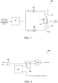
- Figure 7 illustrates a block diagram of an embodiment circuit 700 for testing the uncovered functional combination logic of a digital circuit.
- Circuit 700 includes an XOR tree 702, an inverted-single input OR gate 704, an OR gate 706, a pair of optional multiplexers 708, and an existing D flip-flop 710, which may (or may not) be arranged as shown. Further, circuit 700 may include additional components not shown in Figure 7 .
- an existing D flip-flop set (S) pin may be used to test uncovered functional combination logic.
- An embodiment of this implementation is shown in circuit 700.
- the input to the XOR tree 702 is coupled to uncovered functional combination logic.
- the first output of the XOR tree 702 is coupled to the inverted input of OR gate 704.
- the non-inverting input of the OR gate 704 is coupled to the control signal.
- the output of the OR gate 704 is coupled to the set (S) pin of the existing D flip-flop 710.
- a multiplexer 708 is used when the set (S) pin of the existing D flip-flop 710 is used a priori. The multiplexer 708, thus, allows the proper functioning of the existing D flip-flop 710 during the functional mode.
- a second output of the XOR tree 702 is coupled to an input of the OR gate 706, and a second input of the OR gate 706 is coupled to the control signal.
- the output of the OR gate 706 is coupled to the reset (R) pin of the existing D flip-flop 710.
- a multiplexer 708 is used when the reset (R) pin of the existing D flip-flop 710 is used a priori. The multiplexer 708, thus, allows the proper functioning of the existing D flip-flop 710 during the functional mode.
- circuit 700 a single existing D flip-flop 710 is used to cover two output branches of the XOR tree 702.
- Figure 8 illustrates a block diagram of an embodiment circuit 800 to generate the control signal for testing uncovered functional combination logic of a digital circuit.
- Circuit 800 includes a multiplexer 802, a one-hot decoder circuit 804, a pipeline flip-flop 806, and an OR gate 808, which may (or may not) be arranged as shown. Further, circuit 800 may include additional components not shown in Figure 8 .
- Multiplexer 802 is used to select between (i) a pad of the digital circuit during ATPG functions or functional mode, and (ii) LBIST control mode (e.g., during LBIST functions where the testing of the uncovered functional combination logic is required in both ATPG and LBIST).
- the output of the multiplexer is tied to the pad of the digital circuit with a value of Not Care (N/C) because the pipeline flip-flop 806 is set to "1" at power-up and remains at this value since no clock signal is allowed from the one-hot decoder 804 to the pipeline flip-flop 806.
- N/C Not Care
- the data input of the pipeline flip-flop 806 is coupled to the multiplexer 802.
- the clock input of the pipeline flip-flop 806 is coupled to the output of the one-hot decoder circuit 804.
- the value of the one-hot decoder circuit 804 is loaded during a scan shift (i.e., pipeline flip-flop 806 is set to "1" during power-up and remains “1” during the shift as PAD is forced to "1" during the ATPG scan shift, and LBIST control is forced to "1" during the LBIST scan shift).
- the value of the one-hot decoder circuit 804 is held during the scan capture (i.e., pipeline flip-flop 806 is set to “0” as PAD is forced to “0” during the ATPG scan capture and LBIST control is forced to "0" during the LBIST scan capture).
- the pipeline flip-flop 806 is set to "1" during a power-up sequence of the digital circuit. This sets the control signal at the output of the OR gate 808 at a high level during non-test modes (e.g., functional mode). In embodiments, the pipeline flip-flop 806 does not receive a clock signal from one-hot decoder circuit 804 during non-test modes (e.g., functional mode).
- the OR gate 808 includes a third input coupled to a transition signal.
- the transition signal allows the at-speed testing operation using ATPG or LBIST functions.
- the value of the transition signal is forced to "0" during all other operations, for example, during stuck-at testing, functional mode, and the like.
- Circuit 800 effectively allows the LBIST to dictate the value of the control signal or ATPG signal to dictate the value of PAD during the testing of the uncovered functional combination logic.
- the output of the OR gate 808 is coupled to the inputs of the OR gate 402 in circuit 400, OR gate 504 in circuit 500, OR gate 606 in circuit 600, and the OR gates 704 and 706 in circuit 700.
- circuit 800 is non-limiting and other circuits for generating the control signal are also contemplated.
- the one-hot decoder circuit 804, the OR gate 808, and the pipeline flip-flop 806 are existing components of the digital circuit. Thus, the circuit footprint is not increased by using the existing components to generate the control signal.
- generating the control signal using circuit 800 with the one-hot decoder circuit 804 and the pipeline flip-flop 806 internal to the digital circuit removes the need for a separate control pad in the digital circuit, which results in costs savings in a high-parallelism test environment.
- LBIST is a fully internal test, which does not control a pad of the digital circuit nor is it used to observe the pad.
- the LBIST controller IP input is provided at the output of OR gate 808.
- a single circuit 800 generates a control signal fed (i.e., through a direct or indirect net connection from the output of OR gate 808) to the inputs of the OR gate 402 in circuit 400, OR gate 504 in circuit 500, OR gate 606 in circuit 600, and the OR gates 704 and 706 in circuit 700 for the various digital circuits to test uncovered functional combinational logic.
- the various uncovered functional combinational logic are, thus, tested.
- Figure 9 is a timing diagram of embodiment signals 900 of a digital circuit for testing uncovered functional combination logic.
- Signals 900 include test clock signal 902, pad_lbist signal 904, clock pipe signal 906, pipeline select signal 908, and other clock signal 910.
- Test clock signal 902 is the clock signal used for ATPG and LBIST testing.
- Pad_lbist signal 904 is the signal fed to multiplexer 802 to select between a pad and the LBIST.
- Clock pipe signal 906 is the clock signal from one-hot decoder circuit 804 to the pipeline flip-flop 806.
- Pipeline select signal 908 is the output signal from the pipeline flip-flop 806 to OR gate 808.
- Other clock signal 910 is the clock signal communicated from the one-hot decoder circuit 804 to other portions of the digital circuit.
- test clock signal 902 clock pipe signal 906, and other clock signal 910 operate as a typical clock signal
- pad_lbist signal 904 and pipeline select signal 908 are set to a high level, which sets the control signal at a high level-when the control signal is set to a high level, the uncovered functional combination logic is not being tested.
- the pad_lbist signal 904 is pulled low.
- the one-hot decoder circuit 804 begins control operation.
- Test clock signal 902, clock pipe signal 906, and other clock signal 910 are pulled low.
- the pipeline select signal 908 is pulled low in response to the clock pipe signal 906 being asserted, which results in the control signal being placed in the condition for testing the uncovered functional combination logic of the digital circuit.
- the pipeline select signal 908 is pulled high, which results in the control signal exiting the condition for testing the uncovered functional combination logic of the digital circuit.
- the pipeline select signal 908 remains high, and the other clock signal 910 is used to operate the other portions of the digital circuit.
- Figure 10 illustrates a block diagram of an embodiment processing system 1000.
- the processing system 1000 includes a processor 1002, a memory 1004, and an interface 1006, which may (or may not) be arranged as shown.
- the processing system 1000 may include additional components not depicted, such as long-term storage (e.g., non-volatile memory, etc.), measurement devices, and the like.
- Processor 1002 may be any component or collection of components adapted to perform computations or other processing related tasks, as disclosed herein.
- Memory 1004 may be any component or collection of components adapted to store programming or instructions for execution by the processor 1002.
- memory 1004 includes a non-transitory computer-readable medium.
- Interface 1006 may be any component or collection of components that allow the processor 1002 to communicate with other devices/components or a user.
- interface 1006 may be adapted to allow a user or device (e.g., personal computer (PC), etc.) to interact/communicate with the processing system 1000.
- PC personal computer
Landscapes
- Engineering & Computer Science (AREA)
- General Engineering & Computer Science (AREA)
- Physics & Mathematics (AREA)
- General Physics & Mathematics (AREA)
- Computer Hardware Design (AREA)
- Chemical & Material Sciences (AREA)
- Nanotechnology (AREA)
- Tests Of Electronic Circuits (AREA)
- Semiconductor Integrated Circuits (AREA)
- Computing Systems (AREA)
- Mathematical Physics (AREA)
Applications Claiming Priority (1)
| Application Number | Priority Date | Filing Date | Title |
|---|---|---|---|
| US18/100,975 US12366605B2 (en) | 2023-01-24 | 2023-01-24 | Area, cost, and time-effective scan coverage improvement |
Publications (1)
| Publication Number | Publication Date |
|---|---|
| EP4407327A1 true EP4407327A1 (de) | 2024-07-31 |
Family
ID=89541959
Family Applications (1)
| Application Number | Title | Priority Date | Filing Date |
|---|---|---|---|
| EP24150870.4A Withdrawn EP4407327A1 (de) | 2023-01-24 | 2024-01-09 | Effektive scan-abdeckung |
Country Status (3)
| Country | Link |
|---|---|
| US (1) | US12366605B2 (de) |
| EP (1) | EP4407327A1 (de) |
| CN (1) | CN118393331A (de) |
Citations (2)
| Publication number | Priority date | Publication date | Assignee | Title |
|---|---|---|---|---|
| US20130254609A1 (en) * | 2012-03-22 | 2013-09-26 | Renesas Electronics Corporation | Scan test circuit, test pattern generation control circuit, and scan test control method |
| US20210109153A1 (en) * | 2019-10-15 | 2021-04-15 | Nxp B.V. | Testing of asynchronous reset logic |
Family Cites Families (9)
| Publication number | Priority date | Publication date | Assignee | Title |
|---|---|---|---|---|
| JP3693986B2 (ja) | 2002-09-05 | 2005-09-14 | Necエレクトロニクス株式会社 | バウンダリスキャンテスト回路 |
| JP2009205414A (ja) | 2008-02-27 | 2009-09-10 | Nec Electronics Corp | 半導体集積回路及びその設計方法並びに半導体集積回路設計装置 |
| US7900107B2 (en) | 2008-08-20 | 2011-03-01 | Faraday Technology Corp. | High speed ATPG testing circuit and method |
| JP5297468B2 (ja) | 2008-12-26 | 2013-09-25 | ルネサスエレクトロニクス株式会社 | 半導体集積回路の設計方法およびソフトウエア |
| US7949916B1 (en) | 2009-01-20 | 2011-05-24 | Altera Corporation | Scan chain circuitry for delay fault testing of logic circuits |
| JP2010266417A (ja) | 2009-05-18 | 2010-11-25 | Sony Corp | 半導体集積回路、情報処理装置、および情報処理方法、並びにプログラム |
| US8205125B2 (en) | 2009-10-23 | 2012-06-19 | Texas Instruments Incorporated | Enhanced control in scan tests of integrated circuits with partitioned scan chains |
| TWI684987B (zh) | 2019-05-31 | 2020-02-11 | 創意電子股份有限公司 | 電路校正系統與增加掃描測試涵蓋率的方法 |
| US11681848B2 (en) | 2020-05-12 | 2023-06-20 | Synopsys, Inc. | On-the-fly multi-bit flip flop generation |
-
2023
- 2023-01-24 US US18/100,975 patent/US12366605B2/en active Active
-
2024
- 2024-01-09 EP EP24150870.4A patent/EP4407327A1/de not_active Withdrawn
- 2024-01-23 CN CN202410091865.7A patent/CN118393331A/zh active Pending
Patent Citations (2)
| Publication number | Priority date | Publication date | Assignee | Title |
|---|---|---|---|---|
| US20130254609A1 (en) * | 2012-03-22 | 2013-09-26 | Renesas Electronics Corporation | Scan test circuit, test pattern generation control circuit, and scan test control method |
| US20210109153A1 (en) * | 2019-10-15 | 2021-04-15 | Nxp B.V. | Testing of asynchronous reset logic |
Non-Patent Citations (1)
| Title |
|---|
| MUKHERJEE NILANJAN ET AL: "Test Time and Area Optimized BrST Scheme for Automotive ICs", 2019 IEEE INTERNATIONAL TEST CONFERENCE (ITC), IEEE, 9 November 2019 (2019-11-09), pages 1 - 10, XP033720215, DOI: 10.1109/ITC44170.2019.9000133 * |
Also Published As
| Publication number | Publication date |
|---|---|
| US12366605B2 (en) | 2025-07-22 |
| CN118393331A (zh) | 2024-07-26 |
| US20240250668A1 (en) | 2024-07-25 |
Similar Documents
| Publication | Publication Date | Title |
|---|---|---|
| US5056094A (en) | Delay fault testing method and apparatus | |
| US5570375A (en) | IEEE Std. 1149.1 boundary scan circuit capable of built-in self-testing | |
| KR0156547B1 (ko) | 집적 회로용 검사셀 | |
| US5648973A (en) | I/O toggle test method using JTAG | |
| US6484280B1 (en) | Scan path test support | |
| JP6544772B2 (ja) | スキャンテスト用のテストモード制御信号を生成可能な集積回路 | |
| EP0358365A2 (de) | Prüf-Puffer/Register | |
| CN114667455B (zh) | 用于测试电路的通用压缩器架构 | |
| Serra et al. | Testing | |
| EP3756020B1 (de) | Deterministischer sternförmiger eingebauter selbsttest | |
| US7111217B1 (en) | Method and system for flexibly nesting JTAG TAP controllers for FPGA-based system-on-chip (SoC) | |
| US20090228751A1 (en) | method for performing logic built-in-self-test cycles on a semiconductor chip and a corresponding semiconductor chip with a test engine | |
| US20230120955A1 (en) | Boundary scan test method and storage medium | |
| US7607057B2 (en) | Test wrapper including integrated scan chain for testing embedded hard macro in an integrated circuit chip | |
| US10459029B2 (en) | On-chip clock control monitoring | |
| Cantoro et al. | Automatic generation of stimuli for fault diagnosis in IEEE 1687 networks | |
| Maierhofer | Hierarchical self-test concept based on the JTAG standard | |
| US10247776B2 (en) | Structurally assisted functional test and diagnostics for integrated circuits | |
| EP4407327A1 (de) | Effektive scan-abdeckung | |
| KR0165105B1 (ko) | 개량된 검사 회로 | |
| Ungar et al. | IEEE-1149. X standards: achievements vs. expectations | |
| Bushard et al. | DFT of the Cell Processor and its Impact on EDA Test Softwar | |
| US6650136B2 (en) | Method and apparatus to enhance testability of logic coupled to IO buffers | |
| KR20060095283A (ko) | 다중 시스템 클럭 및 이종 코어를 포함하는 시스템 온 칩용연결선 지연 고장 테스트 제어기 | |
| Nelson et al. | Physical-design-friendly hierarchical logic built-in self-test—A case study |
Legal Events
| Date | Code | Title | Description |
|---|---|---|---|
| PUAI | Public reference made under article 153(3) epc to a published international application that has entered the european phase |
Free format text: ORIGINAL CODE: 0009012 |
|
| STAA | Information on the status of an ep patent application or granted ep patent |
Free format text: STATUS: THE APPLICATION HAS BEEN PUBLISHED |
|
| AK | Designated contracting states |
Kind code of ref document: A1 Designated state(s): AL AT BE BG CH CY CZ DE DK EE ES FI FR GB GR HR HU IE IS IT LI LT LU LV MC ME MK MT NL NO PL PT RO RS SE SI SK SM TR |
|
| STAA | Information on the status of an ep patent application or granted ep patent |
Free format text: STATUS: REQUEST FOR EXAMINATION WAS MADE |
|
| 17P | Request for examination filed |
Effective date: 20250129 |
|
| STAA | Information on the status of an ep patent application or granted ep patent |
Free format text: STATUS: THE APPLICATION HAS BEEN WITHDRAWN |
|
| 18W | Application withdrawn |
Effective date: 20251128 |