EP4404579A1 - Kameramodul und elektronische vorrichtung damit - Google Patents
Kameramodul und elektronische vorrichtung damit Download PDFInfo
- Publication number
- EP4404579A1 EP4404579A1 EP22883826.4A EP22883826A EP4404579A1 EP 4404579 A1 EP4404579 A1 EP 4404579A1 EP 22883826 A EP22883826 A EP 22883826A EP 4404579 A1 EP4404579 A1 EP 4404579A1
- Authority
- EP
- European Patent Office
- Prior art keywords
- magnet
- carrier
- axis
- optical axis
- yoke member
- Prior art date
- Legal status (The legal status is an assumption and is not a legal conclusion. Google has not performed a legal analysis and makes no representation as to the accuracy of the status listed.)
- Pending
Links
Images








Classifications
-
- G—PHYSICS
- G03—PHOTOGRAPHY; CINEMATOGRAPHY; ANALOGOUS TECHNIQUES USING WAVES OTHER THAN OPTICAL WAVES; ELECTROGRAPHY; HOLOGRAPHY
- G03B—APPARATUS OR ARRANGEMENTS FOR TAKING PHOTOGRAPHS OR FOR PROJECTING OR VIEWING THEM; APPARATUS OR ARRANGEMENTS EMPLOYING ANALOGOUS TECHNIQUES USING WAVES OTHER THAN OPTICAL WAVES; ACCESSORIES THEREFOR
- G03B17/00—Details of cameras or camera bodies; Accessories therefor
- G03B17/02—Bodies
- G03B17/12—Bodies with means for supporting objectives, supplementary lenses, filters, masks, or turrets
-
- G—PHYSICS
- G03—PHOTOGRAPHY; CINEMATOGRAPHY; ANALOGOUS TECHNIQUES USING WAVES OTHER THAN OPTICAL WAVES; ELECTROGRAPHY; HOLOGRAPHY
- G03B—APPARATUS OR ARRANGEMENTS FOR TAKING PHOTOGRAPHS OR FOR PROJECTING OR VIEWING THEM; APPARATUS OR ARRANGEMENTS EMPLOYING ANALOGOUS TECHNIQUES USING WAVES OTHER THAN OPTICAL WAVES; ACCESSORIES THEREFOR
- G03B5/00—Adjustment of optical system relative to image or object surface other than for focusing
-
- H—ELECTRICITY
- H02—GENERATION; CONVERSION OR DISTRIBUTION OF ELECTRIC POWER
- H02K—DYNAMO-ELECTRIC MACHINES
- H02K33/00—Motors with reciprocating, oscillating or vibrating magnet, armature or coil system
- H02K33/18—Motors with reciprocating, oscillating or vibrating magnet, armature or coil system with coil systems moving upon intermittent or reversed energisation thereof by interaction with a fixed field system, e.g. permanent magnets
-
- H—ELECTRICITY
- H04—ELECTRIC COMMUNICATION TECHNIQUE
- H04N—PICTORIAL COMMUNICATION, e.g. TELEVISION
- H04N23/00—Cameras or camera modules comprising electronic image sensors; Control thereof
-
- H—ELECTRICITY
- H04—ELECTRIC COMMUNICATION TECHNIQUE
- H04N—PICTORIAL COMMUNICATION, e.g. TELEVISION
- H04N23/00—Cameras or camera modules comprising electronic image sensors; Control thereof
- H04N23/50—Constructional details
- H04N23/51—Housings
-
- H—ELECTRICITY
- H04—ELECTRIC COMMUNICATION TECHNIQUE
- H04N—PICTORIAL COMMUNICATION, e.g. TELEVISION
- H04N23/00—Cameras or camera modules comprising electronic image sensors; Control thereof
- H04N23/50—Constructional details
- H04N23/54—Mounting of pick-up tubes, electronic image sensors, deviation or focusing coils
-
- H—ELECTRICITY
- H04—ELECTRIC COMMUNICATION TECHNIQUE
- H04N—PICTORIAL COMMUNICATION, e.g. TELEVISION
- H04N23/00—Cameras or camera modules comprising electronic image sensors; Control thereof
- H04N23/50—Constructional details
- H04N23/55—Optical parts specially adapted for electronic image sensors; Mounting thereof
-
- H—ELECTRICITY
- H04—ELECTRIC COMMUNICATION TECHNIQUE
- H04N—PICTORIAL COMMUNICATION, e.g. TELEVISION
- H04N23/00—Cameras or camera modules comprising electronic image sensors; Control thereof
- H04N23/57—Mechanical or electrical details of cameras or camera modules specially adapted for being embedded in other devices
-
- H—ELECTRICITY
- H04—ELECTRIC COMMUNICATION TECHNIQUE
- H04N—PICTORIAL COMMUNICATION, e.g. TELEVISION
- H04N23/00—Cameras or camera modules comprising electronic image sensors; Control thereof
- H04N23/60—Control of cameras or camera modules
-
- H—ELECTRICITY
- H04—ELECTRIC COMMUNICATION TECHNIQUE
- H04N—PICTORIAL COMMUNICATION, e.g. TELEVISION
- H04N23/00—Cameras or camera modules comprising electronic image sensors; Control thereof
- H04N23/60—Control of cameras or camera modules
- H04N23/68—Control of cameras or camera modules for stable pick-up of the scene, e.g. compensating for camera body vibrations
- H04N23/682—Vibration or motion blur correction
- H04N23/685—Vibration or motion blur correction performed by mechanical compensation
- H04N23/687—Vibration or motion blur correction performed by mechanical compensation by shifting the lens or sensor position
Definitions
- the disclosure relates to a camera module and an electronic device including the same.
- a mobile electronic device such as a smartphone, may include a camera module.
- the camera module may include lenses, a lens barrel surrounding the lenses, and an image sensor.
- the camera module may support various functions.
- the camera module may support functions related to image stabilization (e.g., optical image stabilization (OIS), digital image stabilization (DIS), or electrical image stabilization (EIS)) and auto focus (AF).
- OIS optical image stabilization
- DIS digital image stabilization
- EIS electrical image stabilization
- AF auto focus
- the camera module may be configured to provide an image stabilization function and an auto focus function by moving the lenses relative to the image sensor.
- the camera module may be configured to move the lenses relative to the image sensor in directions substantially perpendicular to the optical axis of the lenses in relation to the image stabilization function, or may be configured to move the lenses relative to the image sensor in the direction of the optical axis in relation to the auto focus function.
- the camera module may include various types of actuators for implementing the movements of the lenses.
- the actuators may be provided by using a stepping motor (STM), a voice coil motor (VCM), shape memory alloys (SMA), and a piezoelectric motor.
- STM stepping motor
- VCM voice coil motor
- SMA shape memory alloys
- piezoelectric motor a piezoelectric motor
- the camera module may move a lens assembly in the directions substantially perpendicular to the optical axis when the image stabilization function is performed.
- a structure e.g., a lens carrier
- driving forces facing the two directions perpendicular to each other may be applied to the structure.
- the structure may be unintentionally rotated. The unintended rotation may make it difficult to accurately control the position of the lens assembly and may degrade image correction performance.
- a camera module for decreasing a rotational component of a lens assembly by increasing rotational restoring forces using attractive forces acting between yoke members and magnets, and an electronic device including the camera module.
- a camera module includes: a camera housing; a first carrier provided in the camera housing and configured to be movable; a lens; a second carrier having the lens coupled thereto, the second carrier being at least partially provided in the first carrier and configured to move relative to the first carrier in at least one direction substantially perpendicular to an optical axis of the lens; a plurality of magnets provided on the second carrier, the plurality of magnets including a first magnet and a second magnet facing directions perpendicular to each other; and a plurality of yoke members provided on the first carrier and configured to form magnetic attractions with the plurality of magnets, the plurality of yoke members including a first yoke member facing the first magnet and a second yoke member facing the second magnet, wherein the first yoke member includes a first part and a second part spaced apart from the first part in a lengthwise direction of the first magnet, the second yoke member includes a third part and a fourth part spaced apart from
- a camera module includes: a camera housing; a first carrier provided in the camera housing and configured to be movable; a lens; a second carrier having the lens coupled thereto, the second carrier being at least partially provided in the first carrier and configured to move relative to the first carrier in a direction perpendicular to an optical axis of the lens; a first magnet provided on the second carrier and configured to move the second carrier in a direction of a first movement axis perpendicular to the optical axis; a second magnet provided on the second carrier and configured to move the second carrier in a direction of a second movement axis perpendicular to the optical axis and the first movement axis; a first yoke member provided on the first carrier and configured to form a magnetic attraction with the first magnet; and a second yoke member provided on the first carrier and configured to form a magnetic attraction with the second magnet, wherein a first central axis and a second central axis parallel to the optical axis are defined in
- the camera module may include the yoke members, each of which is asymmetrically divided, thereby increasing rotational restoring forces and reducing a rotational component.
- the positions of the yoke members and the magnets may be moved in the directions in which the radius of rotation is increased, and thus the camera module may increase rotational restoring forces and may reduce a rotational component.
- embodiments of the disclosure may provide various effects that are directly or indirectly recognized.
- FIG. 1 is a block diagram illustrating an electronic device 101 in a network environment 100 according to various embodiments.
- the electronic device 101 in the network environment 100 may communicate with an electronic device 102 via a first network 198 (e.g., a short-range wireless communication network), or at least one of an electronic device 104 or a server 108 via a second network 199 (e.g., a long-range wireless communication network).
- a first network 198 e.g., a short-range wireless communication network
- a second network 199 e.g., a long-range wireless communication network
- the electronic device 101 may communicate with the electronic device 104 via the server 108.
- the electronic device 101 may include a processor 120, memory 130, an input module 150, a sound output module 155, a display module 160, an audio module 170, a sensor module 176, an interface 177, a connecting terminal 178, a haptic module 179, a camera module 180, a power management module 188, a battery 189, a communication module 190, a subscriber identification module (SIM) 196, or an antenna module 197.
- at least one of the components e.g., the connecting terminal 178) may be omitted from the electronic device 101, or one or more other components may be added in the electronic device 101.
- some of the components e.g., the sensor module 176, the camera module 180, or the antenna module 197) may be implemented as a single component (e.g., the display module 160).
- the processor 120 may execute, for example, software (e.g., a program 140) to control at least one other component (e.g., a hardware or software component) of the electronic device 101 coupled with the processor 120, and may perform various data processing or computation. According to one embodiment, as at least part of the data processing or computation, the processor 120 may store a command or data received from another component (e.g., the sensor module 176 or the communication module 190) in volatile memory 132, process the command or the data stored in the volatile memory 132, and store resulting data in non-volatile memory 134.
- software e.g., a program 140
- the processor 120 may store a command or data received from another component (e.g., the sensor module 176 or the communication module 190) in volatile memory 132, process the command or the data stored in the volatile memory 132, and store resulting data in non-volatile memory 134.
- the processor 120 may include a main processor 121 (e.g., a central processing unit (CPU) or an application processor (AP)), or an auxiliary processor 123 (e.g., a graphics processing unit (GPU), a neural processing unit (NPU), an image signal processor (ISP), a sensor hub processor, or a communication processor (CP)) that is operable independently from, or in conjunction with, the main processor 121.
- a main processor 121 e.g., a central processing unit (CPU) or an application processor (AP)
- auxiliary processor 123 e.g., a graphics processing unit (GPU), a neural processing unit (NPU), an image signal processor (ISP), a sensor hub processor, or a communication processor (CP)
- the main processor 121 may be adapted to consume less power than the main processor 121, or to be specific to a specified function.
- the auxiliary processor 123 may be implemented as separate from, or as part of the main processor 121.
- the auxiliary processor 123 may control at least some of functions or states related to at least one component (e.g., the display module 160, the sensor module 176, or the communication module 190) among the components of the electronic device 101, instead of the main processor 121 while the main processor 121 is in an inactive (e.g., sleep) state, or together with the main processor 121 while the main processor 121 is in an active state (e.g., executing an application).
- the auxiliary processor 123 e.g., an image signal processor or a communication processor
- the auxiliary processor 123 may include a hardware structure specified for artificial intelligence model processing.
- An artificial intelligence model may be generated by machine learning. Such learning may be performed, e.g., by the electronic device 101 where the artificial intelligence is performed or via a separate server (e.g., the server 108). Learning algorithms may include, but are not limited to, e.g., supervised learning, unsupervised learning, semi-supervised learning, or reinforcement learning.
- the artificial intelligence model may include a plurality of artificial neural network layers.
- the artificial neural network may be a deep neural network (DNN), a convolutional neural network (CNN), a recurrent neural network (RNN), a restricted Boltzmann machine (RBM), a deep belief network (DBN), a bidirectional recurrent deep neural network (BRDNN), deep Q-network or a combination of two or more thereof but is not limited thereto.
- the artificial intelligence model may, additionally or alternatively, include a software structure other than the hardware structure.
- the memory 130 may store various data used by at least one component (e.g., the processor 120 or the sensor module 176) of the electronic device 101.
- the various data may include, for example, software (e.g., the program 140) and input data or output data for a command related thererto.
- the memory 130 may include the volatile memory 132 or the non-volatile memory 134.
- the program 140 may be stored in the memory 130 as software, and may include, for example, an operating system (OS) 142, middleware 144, or an application 146.
- OS operating system
- middleware middleware
- application application
- the input module 150 may receive a command or data to be used by another component (e.g., the processor 120) of the electronic device 101, from the outside (e.g., a user) of the electronic device 101.
- the input module 150 may include, for example, a microphone, a mouse, a keyboard, a key (e.g., a button), or a digital pen (e.g., a stylus pen).
- the sound output module 155 may output sound signals to the outside of the electronic device 101.
- the sound output module 155 may include, for example, a speaker or a receiver.
- the speaker may be used for general purposes, such as playing multimedia or playing record.
- the receiver may be used for receiving incoming calls. According to an embodiment, the receiver may be implemented as separate from, or as part of the speaker.
- the display module 160 may visually provide information to the outside (e.g., a user) of the electronic device 101.
- the display module 160 may include, for example, a display, a hologram device, or a projector and control circuitry to control a corresponding one of the display, hologram device, and projector.
- the display module 160 may include a touch sensor adapted to detect a touch, or a pressure sensor adapted to measure the intensity of force incurred by the touch.
- the audio module 170 may convert a sound into an electrical signal and vice versa. According to an embodiment, the audio module 170 may obtain the sound via the input module 150, or output the sound via the sound output module 155 or a headphone of an external electronic device (e.g., an electronic device 102) directly (e.g., wiredly) or wirelessly coupled with the electronic device 101.
- an external electronic device e.g., an electronic device 102
- directly e.g., wiredly
- wirelessly e.g., wirelessly
- the sensor module 176 may detect an operational state (e.g., power or temperature) of the electronic device 101 or an environmental state (e.g., a state of a user) external to the electronic device 101, and then generate an electrical signal or data value corresponding to the detected state.
- the sensor module 176 may include, for example, a gesture sensor, a gyro sensor, an atmospheric pressure sensor, a magnetic sensor, an acceleration sensor, a grip sensor, a proximity sensor, a color sensor, an infrared (IR) sensor, a biometric sensor, a temperature sensor, a humidity sensor, or an illuminance sensor.
- the interface 177 may support one or more specified protocols to be used for the electronic device 101 to be coupled with the external electronic device (e.g., the electronic device 102) directly (e.g., wiredly) or wirelessly.
- the interface 177 may include, for example, a high definition multimedia interface (HDMI), a universal serial bus (USB) interface, a secure digital (SD) card interface, or an audio interface.
- HDMI high definition multimedia interface
- USB universal serial bus
- SD secure digital
- a connecting terminal 178 may include a connector via which the electronic device 101 may be physically connected with the external electronic device (e.g., the electronic device 102).
- the connecting terminal 178 may include, for example, a HDMI connector, a USB connector, a SD card connector, or an audio connector (e.g., a headphone connector).
- the haptic module 179 may convert an electrical signal into a mechanical stimulus (e.g., a vibration or a movement) or electrical stimulus which may be recognized by a user via his tactile sensation or kinesthetic sensation.
- the haptic module 179 may include, for example, a motor, a piezoelectric element, or an electric stimulator.
- the camera module 180 may capture a still image or moving images.
- the camera module 180 may include one or more lenses, image sensors, image signal processors, or flashes.
- the power management module 188 may manage power supplied to the electronic device 101.
- the power management module 188 may be implemented as at least part of, for example, a power management integrated circuit (PMIC).
- PMIC power management integrated circuit
- the battery 189 may supply power to at least one component of the electronic device 101.
- the battery 189 may include, for example, a primary cell which is not rechargeable, a secondary cell which is rechargeable, or a fuel cell.
- the communication module 190 may support establishing a direct (e.g., wired) communication channel or a wireless communication channel between the electronic device 101 and the external electronic device (e.g., the electronic device 102, the electronic device 104, or the server 108) and performing communication via the established communication channel.
- the communication module 190 may include one or more communication processors that are operable independently from the processor 120 (e.g., the application processor (AP)) and supports a direct (e.g., wired) communication or a wireless communication.
- AP application processor
- the communication module 190 may include a wireless communication module 192 (e.g., a cellular communication module, a short-range wireless communication module, or a global navigation satellite system (GNSS) communication module) or a wired communication module 194 (e.g., a local area network (LAN) communication module or a power line communication (PLC) module).
- a wireless communication module 192 e.g., a cellular communication module, a short-range wireless communication module, or a global navigation satellite system (GNSS) communication module
- GNSS global navigation satellite system
- wired communication module 194 e.g., a local area network (LAN) communication module or a power line communication (PLC) module.
- LAN local area network
- PLC power line communication
- a corresponding one of these communication modules may communicate with the external electronic device via the first network 198 (e.g., a short-range communication network, such as BluetoothTM, wireless-fidelity (Wi-Fi) direct, or infrared data association (IrDA)) or the second network 199 (e.g., a long-range communication network, such as a legacy cellular network, a 5G network, a next-generation communication network, the Internet, or a computer network (e.g., LAN or wide area network (WAN)).
- first network 198 e.g., a short-range communication network, such as BluetoothTM, wireless-fidelity (Wi-Fi) direct, or infrared data association (IrDA)
- the second network 199 e.g., a long-range communication network, such as a legacy cellular network, a 5G network, a next-generation communication network, the Internet, or a computer network (e.g., LAN or wide area network (WAN)).
- the wireless communication module 192 may identify and authenticate the electronic device 101 in a communication network, such as the first network 198 or the second network 199, using subscriber information (e.g., international mobile subscriber identity (IMSI)) stored in the subscriber identification module 196.
- subscriber information e.g., international mobile subscriber identity (IMSI)
- the wireless communication module 192 may support a 5G network, after a 4G network, and next-generation communication technology, e.g., new radio (NR) access technology.
- the NR access technology may support enhanced mobile broadband (eMBB), massive machine type communications (mMTC), or ultra-reliable and low-latency communications (URLLC).
- eMBB enhanced mobile broadband
- mMTC massive machine type communications
- URLLC ultra-reliable and low-latency communications
- the wireless communication module 192 may support a high-frequency band (e.g., the mmWave band) to achieve, e.g., a high data transmission rate.
- the wireless communication module 192 may support various technologies for securing performance on a high-frequency band, such as, e.g., beamforming, massive multiple-input and multiple-output (massive MIMO), full dimensional MIMO (FD-MIMO), array antenna, analog beam-forming, or large scale antenna.
- the wireless communication module 192 may support various requirements specified in the electronic device 101, an external electronic device (e.g., the electronic device 104), or a network system (e.g., the second network 199).
- the wireless communication module 192 may support a peak data rate (e.g., 20Gbps or more) for implementing eMBB, loss coverage (e.g., 164dB or less) for implementing mMTC, or U-plane latency (e.g., 0.5ms or less for each of downlink (DL) and uplink (UL), or a round trip of 1ms or less) for implementing URLLC.
- a peak data rate e.g., 20Gbps or more
- loss coverage e.g., 164dB or less
- U-plane latency e.g., 0.5ms or less for each of downlink (DL) and uplink (UL), or a round trip of 1ms or less
- the antenna module 197 may transmit or receive a signal or power to or from the outside (e.g., the external electronic device) of the electronic device 101.
- the antenna module 197 may include an antenna including a radiating element composed of a conductive material or a conductive pattern formed in or on a substrate (e.g., a printed circuit board (PCB)).
- the antenna module 197 may include a plurality of antennas (e.g., array antennas). In such a case, at least one antenna appropriate for a communication scheme used in the communication network, such as the first network 198 or the second network 199, may be selected, for example, by the communication module 190 (e.g., the wireless communication module 192) from the plurality of antennas.
- the signal or the power may then be transmitted or received between the communication module 190 and the external electronic device via the selected at least one antenna.
- another component e.g., a radio frequency integrated circuit (RFIC)
- RFIC radio frequency integrated circuit
- the antenna module 197 may form a mmWave antenna module.
- the mmWave antenna module may include a printed circuit board, a RFIC disposed on a first surface (e.g., the bottom surface) of the printed circuit board, or adjacent to the first surface and capable of supporting a designated high-frequency band (e.g., the mmWave band), and a plurality of antennas (e.g., array antennas) disposed on a second surface (e.g., the top or a side surface) of the printed circuit board, or adj acent to the second surface and capable of transmitting or receiving signals of the designated high-frequency band.
- a RFIC disposed on a first surface (e.g., the bottom surface) of the printed circuit board, or adjacent to the first surface and capable of supporting a designated high-frequency band (e.g., the mmWave band)
- a plurality of antennas e.g., array antennas
- At least some of the above-described components may be coupled mutually and communicate signals (e.g., commands or data) therebetween via an inter-peripheral communication scheme (e.g., a bus, general purpose input and output (GPIO), serial peripheral interface (SPI), or mobile industry processor interface (MIPI)).
- an inter-peripheral communication scheme e.g., a bus, general purpose input and output (GPIO), serial peripheral interface (SPI), or mobile industry processor interface (MIPI)
- commands or data may be transmitted or received between the electronic device 101 and the external electronic device 104 via the server 108 coupled with the second network 199.
- Each of the electronic devices 102 or 104 may be a device of a same type as, or a different type, from the electronic device 101.
- all or some of operations to be executed at the electronic device 101 may be executed at one or more of the external electronic devices 102, 104, or 108. For example, if the electronic device 101 should perform a function or a service automatically, or in response to a request from a user or another device, the electronic device 101, instead of, or in addition to, executing the function or the service, may request the one or more external electronic devices to perform at least part of the function or the service.
- the one or more external electronic devices receiving the request may perform the at least part of the function or the service requested, or an additional function or an additional service related to the request, and transfer an outcome of the performing to the electronic device 101.
- the electronic device 101 may provide the outcome, with or without further processing of the outcome, as at least part of a reply to the request.
- a cloud computing, distributed computing, mobile edge computing (MEC), or client-server computing technology may be used, for example.
- the electronic device 101 may provide ultra low-latency services using, e.g., distributed computing or mobile edge computing.
- the external electronic device 104 may include an internet-of-things (IoT) device.
- the server 108 may be an intelligent server using machine learning and/or a neural network.
- the external electronic device 104 or the server 108 may be included in the second network 199.
- the electronic device 101 may be applied to intelligent services (e.g., smart home, smart city, smart car, or healthcare) based on 5G communication technology or IoT-related technology.
- FIG. 2 is a block diagram illustrating the camera module according to various embodiments.
- the camera module 180 may include a lens assembly 210, a flash 220, an image sensor 230, an image stabilizer 240, memory 250 (e.g., buffer memory), or an image signal processor 260.
- the lens assembly 210 may collect light emitted or reflected from an object whose image is to be taken.
- the lens assembly 210 may include one or more lenses.
- the camera module 180 may include a plurality of lens assemblies 210. In such a case, the camera module 180 may form, for example, a dual camera, a 360-degree camera, or a spherical camera. Some of the plurality of lens assemblies 210 may have the same lens attribute (e.g., view angle, focal length, auto-focusing, f number, or optical zoom), or at least one lens assembly may have one or more lens attributes different from those of another lens assembly.
- the lens assembly 210 may include, for example, a wide-angle lens or a telephoto lens.
- the flash 220 may emit light that is used to reinforce light reflected from an object.
- the flash 220 may include one or more light emitting diodes (LEDs) (e.g., a red-green-blue (RGB) LED, a white LED, an IR LED, or an ultraviolet (UV) LED) or a xenon lamp.
- LEDs light emitting diodes
- RGB red-green-blue
- UV ultraviolet
- the image sensor 230 may obtain an image corresponding to an object by converting light emitted or reflected from the object and transmitted via the lens assembly 210 into an electrical signal.
- the image sensor 230 may include one selected from image sensors having different attributes, such as a RGB sensor, a black-and-white (BW) sensor, an IR sensor, or a UV sensor, a plurality of image sensors having the same attribute, or a plurality of image sensors having different attributes.
- Each image sensor included in the image sensor 230 may be implemented using, for example, a charged coupled device (CCD) sensor or a complementary metal oxide semiconductor (CMOS) sensor.
- CCD charged coupled device
- CMOS complementary metal oxide semiconductor
- the image stabilizer 240 may move the image sensor 230 or at least one lens included in the lens assembly 210 in a particular direction, or control an operational attribute (e.g., adjust the read-out timing) of the image sensor 230 in response to the movement of the camera module 180 or the electronic device 101 including the camera module 180. This allows compensating for at least part of a negative effect (e.g., image blurring) by the movement on an image being captured.
- the image stabilizer 240 may sense such a movement by the camera module 180 or the electronic device 101 using a gyro sensor (not shown) or an acceleration sensor (not shown) disposed inside or outside the camera module 180.
- the image stabilizer 240 may be implemented, for example, as an optical image stabilizer.
- the memory 250 may store, at least temporarily, at least part of an image obtained via the image sensor 230 for a subsequent image processing task. For example, if image capturing is delayed due to shutter lag or multiple images are quickly captured, a raw image obtained (e.g., a Bayer-patterned image, a high-resolution image) may be stored in the memory 250, and its corresponding copy image (e.g., a low-resolution image) may be previewed via the display module 160. Thereafter, if a specified condition is met (e.g., by a user's input or system command), at least part of the raw image stored in the memory 250 may be obtained and processed, for example, by the image signal processor 260. According to an embodiment, the memory 250 may be configured as at least part of the memory 130 or as a separate memory that is operated independently from the memory 130.
- a raw image obtained e.g., a Bayer-patterned image, a high-resolution image
- its corresponding copy image e.g., a low-
- the image signal processor 260 may perform one or more image processing with respect to an image obtained via the image sensor 230 or an image stored in the memory 250.
- the one or more image processing may include, for example, depth map generation, three-dimensional (3D) modeling, panorama generation, feature point extraction, image synthesizing, or image compensation (e.g., noise reduction, resolution adjustment, brightness adjustment, blurring, sharpening, or softening).
- the image signal processor 260 may perform control (e.g., exposure time control or read-out timing control) with respect to at least one (e.g., the image sensor 230) of the components included in the camera module 180.
- An image processed by the image signal processor 260 may be stored back in the memory 250 for further processing, or may be provided to an external component (e.g., the memory 130, the display module 160, the electronic device 102, the electronic device 104, or the server 108) outside the camera module 180.
- an external component e.g., the memory 130, the display module 160, the electronic device 102, the electronic device 104, or the server 1028 outside the camera module 180.
- the image signal processor 260 may be configured as at least part of the processor 120, or as a separate processor that is operated independently from the processor 120. If the image signal processor 260 is configured as a separate processor from the processor 120, at least one image processed by the image signal processor 260 may be displayed, by the processor 120, via the display module 160 as it is or after being further processed.
- the electronic device 101 may include a plurality of camera modules 180 having different attributes or functions.
- at least one of the plurality of camera modules 180 may form, for example, a wide-angle camera and at least another of the plurality of camera modules 180 may form a telephoto camera.
- at least one of the plurality of camera modules 180 may form, for example, a front camera and at least another of the plurality of camera modules 180 may form a rear camera.
- FIG. 3A is a front perspective view of an electronic device according to an embodiment.
- FIG. 3B is a rear perspective view of the electronic device according to an embodiment.
- FIG. 3C is an exploded perspective view of the electronic device according to an embodiment.
- the electronic device 300 may include a housing 310 that includes a first surface (or, a front surface) 310A, a second surface (or, a rear surface) 310B, and a third surface (or, a side surface) 310C surrounding a space between the first surface 310A and the second surface 310B.
- the housing 310 may refer to a structure that forms some of the first surface 310A, the second surface 310B, and the third surface 310C.
- the first surface 310A may be formed by a front plate 302, at least a portion of which is substantially transparent (e.g., a glass plate including various coating layers, or a polymer plate).
- the second surface 310B may be formed by a back plate 311 that is substantially opaque.
- the back plate 311 may be formed of, for example, coated or colored glass, ceramic, a polymer, metal (e.g., aluminum, stainless steel (STS), or magnesium), or a combination of at least two of the aforementioned materials.
- the third surface 310C may be formed by a side bezel structure (or, a side member) 318 that is coupled with the front plate 302 and the back plate 311 and that contains metal and/or a polymer.
- the back plate 311 and the side bezel structure 318 may be integrally formed with each other and may contain the same material (e.g., a metallic material such as aluminum).
- the front plate 302 may include two first areas 310D that curvedly and seamlessly extend from partial areas of the first surface 310A toward the back plate 311.
- the first areas 310D may be located at opposite long edges of the front plate 302.
- the back plate 311 may include two second areas 310E that curvedly and seamlessly extend from partial areas of the second surface 310B toward the front plate 302.
- the second areas 310E may be located at opposite long edges of the back plate 311.
- the front plate 302 (or, the back plate 311) may include only one of the first areas 310D (or, the second areas 310E). Furthermore, in another embodiment, the front plate 302 (or, the back plate 311) may not include a part of the first areas 310D (or, the second areas 310E).
- the side bezel structure 318 when viewed from a side of the electronic device 300, may have a first thickness (or, width) at sides (e.g., short sides) not including the first areas 310D or the second areas 310E and may have a second thickness at sides (e.g., long sides) including the first areas 310D or the second areas 310E, the second thickness being smaller than the first thickness.
- the electronic device 300 may include at least one of a display 301 (e.g., the display module 160 of FIG. 1 ), audio modules 303, 304, and 307 (e.g., the audio module 170 of FIG. 1 ), a sensor module (not illustrated) (e.g., the sensor module 176 of FIG. 1 ), camera modules 305, 312, and 313 (e.g., the camera module 180 of FIG. 1 ), key input devices 317 (e.g., the input device 150 of FIG. 1 ), a light emitting element (not illustrated), or a connector hole 308 (e.g., the connecting terminal 178 of FIG. 1 ).
- a display 301 e.g., the display module 160 of FIG. 1
- audio modules 303, 304, and 307 e.g., the audio module 170 of FIG. 1
- a sensor module not illustrated
- camera modules 305, 312, and 313 e.g., the camera module 180 of FIG. 1
- At least one component e.g., the key input devices 317 or the light emitting element (not illustrated) among the aforementioned components may be omitted from the electronic device 300, or other component(s) may be additionally included in the electronic device 300.
- the display 301 may be visually exposed through most of the front plate 302. For example, at least a portion of the display 301 may be visually exposed through the front plate 302 that includes the first surface 310A and the first areas 310D of the third surface 310C.
- the display 301 may be disposed on the rear surface of the front plate 302.
- the periphery of the display 301 may be formed to be substantially the same as the shape of the adjacent outside edge of the front plate 302. In another embodiment, to expand the area by which the display 301 is visually exposed, the gap between the outside edge of the display 301 and the outside edge of the front plate 302 may be substantially constant.
- a surface of the housing 310 may include a screen display area that is formed as the display 301 is visually exposed.
- the screen display area may include the first surface 310A and the first areas 310D of the side surface 310C.
- the screen display area 310A and 310D may include a sensing area (not illustrated) that is configured to obtain biometric information of a user.
- a sensing area (not illustrated) that is configured to obtain biometric information of a user.
- the sensing area may refer to an area capable of displaying visual information by the display 301 like the other areas of the screen display area 310A and 310D and additionally obtaining biometric information (e.g., a fingerprint) of the user.
- the screen display area 310A and 310D of the display 301 may include an area through which the first camera module 305 (e.g., a punch hole camera) is visually exposed.
- the first camera module 305 e.g., a punch hole camera
- the first camera module 305 may include a plurality of camera modules (e.g., the camera module 180 of FIG. 1 ).
- the display 301 may be configured such that at least one of an audio module (not illustrated), a sensor module (not illustrated), a camera module (e.g., the first camera module 305), or a light emitting element (not illustrated) is disposed on the rear surface of the screen display area 310A and 310D.
- an audio module not illustrated
- a sensor module not illustrated
- a camera module e.g., the first camera module 305
- a light emitting element not illustrated
- the electronic device 300 may be configured such that the first camera module 305 (e.g., an under display camera (UDC)) is disposed on the rear side (e.g., the side facing the -z-axis direction) of the first surface 310A (e.g., the front surface) and/or the side surface 310C (e.g., at least one surface of the first areas 310D) so as to face toward the first surface 310A and/or the side surface 310C.
- the first camera module 305 may be disposed under the display 301 and may not be visually exposed through the screen display area 310A and 310D.
- the area of the display 301 that faces the first camera module 305 may be formed to be a transmissive area that has a specified transmittance as a portion of the display area that displays contents.
- the transmissive area may have a transmittance of about 5% to about 50%.
- the transmissive area may include an area through which light for generating an image by being focused on an image sensor (e.g., the image sensor 230 of FIG. 2 ) passes and that overlaps an effective area (e.g., a field of view (FOV) area) of the first camera module 305.
- the transmissive area of the display 301 may include an area having a lower pixel density and/or wiring density than a surrounding area.
- the display 301 may be coupled with, or disposed adjacent to, touch detection circuitry, a pressure sensor capable of measuring the intensity (pressure) of a touch, and/or a digitizer that detects a stylus pen of a magnetic field type.
- the audio modules 303, 304, and 307 may include the microphone holes 303 and 304 and the speaker hole 307.
- the microphone holes 303 and 304 may include the first microphone hole 303 formed in a partial area of the third surface 310C and the second microphone hole 304 formed in a partial area of the second surface 310B.
- a microphone (not illustrated) for obtaining external sound may be disposed in the microphone holes 303 and 304.
- the microphone may include a plurality of microphones to sense the direction of sound.
- the second microphone hole 304 formed in the partial area of the second surface 310B may be disposed adjacent to the camera modules 305, 312, and 313.
- the second microphone hole 304 may obtain sounds when the camera modules 305, 312, and 313 are executed, or may obtain sounds when other functions are executed.
- the speaker hole 307 may include an external speaker hole 307 and a receiver hole for telephone call (not illustrated).
- the external speaker hole 307 may be formed in a portion of the third surface 310C of the electronic device 300.
- the external speaker hole 307, together with the microphone hole 303, may be implemented as a single hole.
- the receiver hole for telephone call (not illustrated) may be formed in another portion of the third surface 310C.
- the receiver hole for telephone call may be formed in another portion (e.g., a portion facing the +y-axis direction) of the third surface 310C that faces the portion (e.g., a portion facing the -y-axis direction) of the third surface 310C in which the external speaker hole 307 is formed.
- the receiver hole for telephone call may not be formed in a portion of the third surface 310C and may be formed by a separation space between the front plate 302 (or, the display 301) and the side bezel structure 318.
- the electronic device 300 may include at least one speaker (not illustrated) that is configured to output sound outside the housing 310 through the external speaker hole 307 or the receiver hole for telephone call (not illustrated).
- the speaker may include a piezoelectric speaker from which the speaker hole 307 is omitted.
- the sensor module may generate an electrical signal or a data value that corresponds to an operational state inside the electronic device 300 or an environmental state external to the electronic device 300.
- the sensor module may include at least one of a proximity sensor, a heart rate monitor (HRM) sensor, a fingerprint sensor, a gesture sensor, a gyro sensor, an atmospheric pressure sensor, a magnetic sensor, an acceleration sensor, a grip sensor, a color sensor, an IR sensor, a biosensor, a temperature sensor, a humidity sensor, or an illuminance sensor.
- HRM heart rate monitor
- the camera modules 305, 312, and 313 may include the first camera module 305 (e.g., a punch hole camera) exposed on the first surface 310A of the electronic device 300, the second camera module 312 exposed on the second surface 310B, and/or the flash 313.
- first camera module 305 e.g., a punch hole camera
- second camera module 312 exposed on the second surface 310B
- the first camera module 305 may be visually exposed through a portion of the screen display area 310A and 310D of the display 301.
- the first camera module 305 may be visually exposed on a partial region of the screen display area 310A and 310D through an opening (not illustrated) that is formed in a portion of the display 301.
- the first camera module 305 e.g., an under display camera
- the second camera module 312 may include a plurality of cameras (e.g., a dual camera, a triple camera, or a quad camera). However, the second camera module 312 is not necessarily limited to including the plurality of cameras and may include one camera.
- the first camera module 305 and the second camera module 312 may include one or more lenses, an image sensor, and/or an image signal processor.
- the flash 313 may include, for example, a light emitting diode or a xenon lamp.
- two or more lenses (an IR camera lens, a wide angle lens, and a telephoto lens) and image sensors may be disposed on one surface of the electronic device 300.
- the key input devices 317 may be disposed on the third surface 310C of the housing 310 (e.g., the first areas 310D and/or the second areas 310E).
- the electronic device 300 may not include all or some of the key input devices 317, and the key input devices 317 not included may be implemented in a different form, such as a soft key, on the display 301.
- the key input devices 317 may include a sensor module (not illustrated) that forms the sensing area (not illustrated) that is included in the screen display area 310A and 310D.
- the connector hole 308 may accommodate a connector.
- the connector hole 308 may be disposed in the third surface 310C of the housing 310.
- the connector hole 308 may be disposed in the third surface 310C so as to be adjacent to at least a part of the audio modules (e.g., the microphone hole 303 and the speaker hole 307).
- the electronic device 300 may include the first connector hole 308 capable of accommodating a connector (e.g., a USB connector) for transmitting/receiving power and/or data with an external electronic device, and/or a second connector hole (not illustrated) capable of accommodating a connector (e.g., an earphone jack) for transmitting/receiving audio signals with an external electronic device.
- the electronic device 300 may include the light emitting element (not illustrated).
- the light emitting element (not illustrated) may be disposed on the first surface 310A of the housing 310.
- the light emitting element (not illustrated) may provide state information of the electronic device 300 in the form of light.
- the light emitting element (not illustrated) may provide a light source that operates in conjunction with operation of the first camera module 305.
- the light emitting element (not illustrated) may include an LED, an IR LED, and/or a xenon lamp.
- the electronic device 300 may include a front plate 320 (e.g., the front plate 302 of FIG. 3A ), a display 330 (e.g., the display 301 of FIG. 3A ), a side member 340 (e.g., the side bezel structure 318 of FIG. 3A ), a printed circuit board 350, a rear case 360, a battery 370, a back plate 380 (e.g., the back plate 311 of FIG. 3B ), and an antenna (not illustrated).
- a front plate 320 e.g., the front plate 302 of FIG. 3A
- a display 330 e.g., the display 301 of FIG. 3A
- a side member 340 e.g., the side bezel structure 318 of FIG. 3A
- a printed circuit board 350 e.g., a rear case 360, a battery 370, a back plate 380 (e.g., the back plate 311 of FIG. 3B ), and an antenna (
- the electronic device 300 may not include at least one component (e.g., the rear case 360) among the aforementioned components, or may additionally include other component(s).
- Some of the components of the electronic device 300 illustrated in FIG. 3C may be identical or similar to some of the components of the electronic device 300 illustrated in FIGS. 3A and 3B , and repetitive descriptions will hereinafter be omitted.
- the front plate 320 and the display 330 may be coupled to the side member 340.
- the front plate 320 and the display 330 may be disposed under the side member 340.
- the front plate 320 and the display 330 may be located in the +z-axis direction from the side member 340.
- the display 330 may be coupled to the bottom of the side member 340, and the front plate 320 may be coupled to the bottom of the display 330.
- the front plate 320 may form a portion of the outer surface (or, the exterior) of the electronic device 300.
- the display 330 may be disposed between the front plate 320 and the side member 340 so as to be located inside the electronic device 300.
- the side member 340 may be disposed between the display 330 and the back plate 380.
- the side member 340 may be configured to surround a space between the back plate 380 and the display 330.
- the side member 340 may include a frame structure 341 that forms a portion of the side surface of the electronic device 300 (e.g., the third surface 310C of FIG. 3A ) and a plate structure 342 extending inward from the frame structure 341.
- the plate structure 342 may be disposed inside the frame structure 341 so as to be surrounded by the frame structure 341.
- the plate structure 342 may be connected with the frame structure 341, or may be integrally formed with the frame structure 341.
- the plate structure 342 may be formed of a metallic material and/or a nonmetallic (e.g., polymer) material.
- the plate structure 342 may support other components included in the electronic device 300. For example, at least one of the display 330, the printed circuit board 350, the rear case 360, or the battery 370 may be disposed on the plate structure 342.
- the display 330 may be coupled to one surface (e.g., the surface facing the +z-axis direction) of the plate structure 342, and the printed circuit board 350 may be coupled to an opposite surface (e.g., the surface facing the -z-axis direction) that faces away from the one surface.
- one surface e.g., the surface facing the +z-axis direction
- the printed circuit board 350 may be coupled to an opposite surface (e.g., the surface facing the -z-axis direction) that faces away from the one surface.
- the rear case 360 may be disposed between the back plate 380 and the plate structure 342.
- the rear case 360 may be coupled to the side member 340 so as to overlap at least a portion of the printed circuit board 350.
- the rear case 360 may face the plate structure 342 with the printed circuit board 350 therebetween.
- a processor e.g., the processor 120 of FIG. 1
- memory e.g., the memory 130 of FIG. 1
- an interface e.g., the interface 177 of FIG. 1
- the processor may include, for example, one or more of a central processing unit, an application processor, a graphic processing unit, an image signal processor, a sensor hub processor, or a communication processor.
- the memory may include, for example, volatile memory or nonvolatile memory.
- the interface may include, for example, a HDMI, a USB interface, an SD card interface, and/or an audio interface.
- the interface may electrically or physically connect the electronic device 300 with an external electronic device and may include a USB connector, an SD card/MultiMediaCard (MMC) connector, or an audio connector.
- MMC MultiMediaCard
- the battery 370 may supply power to at least one component of the electronic device 300.
- the battery 370 may include a primary cell that is not rechargeable, a secondary cell that is rechargeable, or a fuel cell. At least a portion of the battery 370 may be disposed on substantially the same plane as the printed circuit board 350.
- the battery 370 may be integrally disposed inside the electronic device 300, or may be disposed to be detachable from the electronic device 300.
- the antenna (not illustrated) (e.g., the antenna module 197 of FIG. 1 ) may be disposed between the back plate 380 and the battery 370.
- the antenna may include, for example, a near field communication (NFC) antenna, a wireless charging antenna, and/or a magnetic secure transmission (MST) antenna.
- NFC near field communication
- MST magnetic secure transmission
- the antenna (not illustrated) may perform short-range communication with an external device, or may wirelessly transmit and receive power required for charging.
- the first camera module 305 may be disposed on at least a portion (e.g., the plate structure 342) of the side member 340 such that a lens receives external light through a partial area of the front plate 320 (e.g., the front surface 310A of FIG. 3A ).
- the lens of the first camera module 305 may be visually exposed through a partial area of the front plate 320.
- a camera area 337 e.g., an opening area or a light transmitting area
- corresponding to the first camera module 305 may be formed in the display 330.
- the second camera module 312 may be disposed on the printed circuit board 350 such that a lens receives external light through a camera area 384 of the back plate 380 (e.g., the rear surface 310B of FIG. 3B ) of the electronic device 300.
- the lens of the second camera module 312 may be visually exposed through the camera area 384.
- the second camera module 312 may be disposed in at least a portion of an inner space formed in the housing of the electronic device 300 (e.g., the housing 310 of FIGS. 3A and 3B ) and may be electrically connected to the printed circuit board 350 through a connecting member (e.g., a connector).
- a connecting member e.g., a connector
- the camera area 384 may be formed in a surface of the back plate 380 (e.g., the rear surface 310B of FIG. 3B ). In an embodiment, the camera area 384 may be formed to be at least partially transparent such that external light is incident on the lens of the second camera module 312. In an embodiment, at least a portion of the camera area 384 may protrude to a predetermined height from the surface of the back plate 380. However, without being necessarily limited thereto, the camera area 384 may form substantially the same plane as the surface of the back plate 380.
- FIG. 4 is a perspective view of a camera module according to an embodiment.
- the camera module 400 may include a camera housing 410, a lens assembly 420 (e.g., the lens assembly 210 of FIG. 2 ), a lens carrier 450, and a substrate member 480.
- the camera module 400 may be configured to receive external light through a partial area of a surface of an electronic device (e.g., the electronic device 300 of FIGS. 3A to 3C ).
- the camera housing 410 may provide a predetermined space in which other components of the camera module 400 are accommodated.
- the camera housing 410 may include a frame 411 and a cover 413 coupled to the frame 411.
- the frame 411 and the cover 413 may be coupled with each other to form an inner space in which at least a portion of the lens assembly 420 and at least a portion of the lens carrier 450 are accommodated.
- At least a portion of the lens assembly 420 and at least a portion of the lens carrier 450 may be accommodated in the frame 411, and the cover 413 may be coupled to the frame 411 to cover at least a portion of the lens assembly 420 and at least a portion of the lens carrier 450.
- the frame 411 may support the lens assembly 420 and the lens carrier 450 disposed therein.
- the substrate member 480 having an image sensor (e.g., the image sensor 230 of FIG. 2 ) electrically connected thereto may be disposed on the frame 411.
- the substrate member 480 having the image sensor 230 mounted thereon may be disposed on the lower surface (or, the bottom surface) (e.g., the surface facing the -z-axis direction) of the frame 411.
- the frame 411 may have, in the lower surface thereof, an opening (not illustrated) through which light passing through a lens 421 is incident on the image sensor 230.
- the cover 413 may have an opening 4131 formed therein through which at least a portion of the lens assembly 420 is visually exposed outside the camera module 410.
- the opening 4131 may be formed in the upper surface (e.g., the surface facing the +z-axis direction) of the cover 413 such that the lens 421 and at least a portion of a lens barrel 423 are exposed outside the camera housing 410.
- the opening 4131 may be at least partially aligned with an optical axis OA of the lens 421.
- the opening 4131 may overlap the lens assembly 420 in the direction of the optical axis OA.
- At least a portion of the lens assembly 420 may be accommodated in the camera housing 410.
- a portion of the lens assembly 420 may protrude outside the camera housing 410 through the opening 4131.
- At least a portion of the lens assembly 420 may be exposed outside the camera housing 410 through the opening 4131 of the cover 413, and thus external light may be incident on the lens 421.
- the lens assembly 420 may include the lens 421 and the lens barrel 423 in which the lens 421 is accommodated.
- the lens barrel 423 may surround one or more lenses 421.
- the lens barrel 423 may provide a function of supporting the lenses 421 and protecting the lenses 421 from an external impact.
- the lens assembly 420 may be accommodated in the camera housing 410 in the state of being coupled to the lens carrier 450.
- the lens assembly 420 may be coupled to (or, mounted on) at least a portion of the lens carrier 450 and may be configured to move together with the lens carrier 450 relative to the camera housing 410.
- the lens assembly 420 may move relative to the camera housing 410 in the direction of the optical axis OA (e.g., the z-axis direction) and/or one or more directions (e.g., the x-axis direction and/or the y-axis direction) substantially perpendicular to the optical axis OA.
- the lens carrier 450 may be coupled with the lens assembly 420 and may be configured to move the lens assembly 420 relative to the camera housing 410 (or, the image sensor 230 fixed to the camera housing 410).
- the lens carrier 450 may be disposed in the camera housing 410 such that at least a portion of the lens carrier 450 is movable relative to the camera housing 410 in the direction of the optical axis OA or the directions substantially perpendicular to the optical axis OA.
- all or part of the lens carrier 450 may move in the direction of the optical axis OA and/or the directions substantially perpendicular to the optical axis OA in the state in which the lens carrier 450 is partially accommodated in the camera housing 410, and the lens assembly 420 may move together with the lens carrier 450.
- the substrate member 480 may be coupled to the frame 411.
- the substrate member 480 may be attached to the bottom surface (e.g., the surface facing the -z-axis direction) of the frame 411, and thus the substrate member 480 may be fixed to the camera housing 410.
- the substrate member 480 may include a sensor board 481 having the image sensor (e.g., the image sensor 230 of FIG. 2 ) disposed thereon, a connecting member 482 extending from the sensor board 481, and a connector 483 formed on the connecting member 482.
- the image sensor 230 may be disposed on the upper surface (e.g., the surface facing the +z-axis direction) of the sensor board 481.
- the image sensor 230 may be disposed on the upper surface of the sensor board 481 to overlap the lens 421 in the direction of the optical axis OA.
- the image sensor 230 may be electrically connected with the sensor board 481.
- the image sensor 230 may covert an optical signal received through the lens 421 into an electrical signal.
- the image sensor 230 may be fixed to the camera housing 410 as the sensor board 481 is coupled with the frame 411, and when the lens assembly 420 moves relative to the camera housing 410, the relative positions of the image sensor 230 and the lens 421 may be changed.
- the substrate member 480 may be electrically connected with the electronic device 300 through the connecting member 482 and the connector 483.
- the connecting member 482 may extend from the sensor board 481 toward the main board of the electronic device 300 (e.g., the printed circuit board 350 of FIG. 3C ), and the connector 483 may be coupled to the main board 350.
- the connecting member 482 and the connector 483 may electrically connect electrical components (e.g., the image sensor 230, the sensor board 481, or coils (e.g., coils 462, 464, and 466 of FIG. 6 )) included in the camera module 400 with the main board 350 of the electronic device 300.
- the sensor board 481 may include a PCB
- the connecting member 482 may include a flexible printed circuit board (FPCB).
- the camera module 400 may provide an auto focus (AF) function and an optical image stabilization (OIS) function by controlling a movement of the lens carrier 450.
- the camera module 400 may be configured to perform the auto focus function by moving the entire lens carrier 450 in the direction of the optical axis OA.
- the camera module 400 may provide the optical image stabilization function (e.g., a camera-shake correction function) by moving a portion of the lens carrier 450 in the directions substantially perpendicular to the optical axis OA.
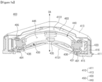
- FIG. 5A is a sectional perspective view of the camera module according to an embodiment.
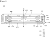
- FIG. 5B is a sectional view of the camera module according to an embodiment.
- FIGS. 5A and 5B may be views in which the lens assembly (e.g., the lens assembly 420 of FIG. 4 ) and the substrate member (e.g., the substrate member 480 of FIG. 4 ) are omitted.
- the lens assembly e.g., the lens assembly 420 of FIG. 4
- the substrate member e.g., the substrate member 480 of FIG. 4
- the camera module 400 may include the camera housing 410, the lens carrier 450, a stopper 493, and a first ball 491. At least some of the components of the camera module 400 illustrated in FIGS. 5A and 5B may be identical or similar to some of the components of the camera module 400 illustrated in FIG. 4 , and repetitive descriptions will hereinafter be omitted.
- the camera housing 410 may include the frame 411 in which the lens carrier 450 is disposed and the cover 413 coupled to the frame 411.
- the frame 411 and the cover 413 may form a space in which the lens carrier 450 and the stopper 493 are disposed.
- the frame 411 may include a plate 415 and a sidewall 416 substantially vertically extending from the plate 415.
- the plate 415 and the sidewall 416 may form a space in which the lens carrier 450 is disposed.
- the plate 415 may support the lens carrier 450, and the sidewall 416 may surround at least a part (e.g., a first carrier 430) of the lens carrier 450.
- the plate 415 may have a first opening 4151 formed therein through which the lens coupled to the lens carrier 450 (e.g., the lens 421 of the lens assembly 420 of FIG. 4 ) faces the image sensor 230.
- the sensor board e.g., the sensor board 481 of FIG.
- the image sensor e.g., the image sensor 230 of FIG. 2
- the image sensor e.g., the image sensor 230 of FIG. 2
- the plate 415 e.g., refer to FIG. 4
- light passing through the lens 421 may be incident on the image sensor 230 through the first opening 4151.
- the cover 413 may be formed such that one portion is coupled to the sidewall 416 of the frame 411 and another portion faces the plate 415.
- the cover 413 may have the second opening 4131 formed therein to partially overlap the first opening 4151 in the direction of the optical axis OA. External light may be incident on the lens 421 through the second opening 4131.
- the cover 413 may perform a function of shielding electromagnetic interference (EMI).
- EMI shielding electromagnetic interference
- the cover 413 may be formed of a metallic material and may be referred to as a shield can (or, an EMI shield can).
- the material of the cover 413 is not limited to metal.
- the lens carrier 450 may include the first carrier 430 disposed in the frame 411 of the camera housing 410 and a second carrier 440 disposed in the first carrier 430.
- the first carrier 430 may be disposed to be movable in the frame 411
- the second carrier 440 may be disposed to be movable in the first carrier 430.
- the first carrier 430 may be disposed in the frame 411.
- the first carrier 430 may be supported by the plate 415 of the frame 411 and may be surrounded by the sidewall 416 of the frame 411.
- the second carrier 440 and at least a portion of the lens assembly (e.g., the lens assembly 420 of FIG. 4 ) coupled to the second carrier 440 may be disposed in the first carrier 430.
- the first carrier 430 may surround a portion of the second carrier 440 and a portion of the lens assembly 420.
- the first carrier 430 may have a first receiving hole 435 formed therein in which at least a portion of the lens assembly 420 is disposed.
- one portion of the lens assembly 420 may be coupled to the second carrier 440 and may be surrounded by a second receiving hole 446 of the second carrier 440, and another portion of the lens assembly 420 may be surrounded by the first receiving hole 435 of the first carrier 430.
- the first carrier 430 may move relative to the camera housing 410 in the direction of the optical axis OA.
- the first carrier 430 may move in the direction of the optical axis OA with respect to the frame 411.
- the second carrier 440 and the lens assembly 420 disposed in the first carrier 430 may move together with the first carrier 430.
- the distance between the image sensor 230 fixed to the frame 411 and the lens assembly 420 (or, the lens 421) may vary, and thus an auto focus function may be performed.
- the first carrier 430 may include a base part 431 and a sidewall part 433 substantially vertically extending from the base part 431.
- the base part 431 and the sidewall part 433 may form a space in which the second carrier 440 is disposed.
- the base part 431 may have the first receiving hole 435 formed therein in which the lens assembly 420 is disposed.
- the base part 431 of the first carrier 430 may at least partially face the plate 415 of the camera housing 410 (e.g., the frame 411).
- the sidewall part 433 of the first carrier 430 may partially face the sidewall 416 of the camera housing 410 (e.g., the frame 411).
- a guide ball e.g., a second ball 492 of FIG. 8
- a guide ball for guiding a movement of the first carrier 430 in the direction of the optical axis OA may be disposed in at least a portion of the space between the sidewall part 433 of the first carrier 430 and the sidewall 416 of the frame 411 (e.g., refer to FIG. 8 ).
- At least one first ball 491 for guiding a movement of the second carrier 440 may be disposed on the base part 431 of the first carrier 430.
- the first ball 491 may be disposed between the first carrier 420 and the second carrier 440 and may be brought into contact with the first carrier 430 and the second carrier 440.
- a ball receiving portion 436 for accommodating the first ball 491 may be formed on the base part 431. The first ball 491 may move while rotating in the ball receiving portion 436.
- the first ball 491 may provide a rolling frictional force between the base part 431 and the second carrier 440 when the second carrier 440 moves relative to the first carrier 430 in directions (e.g., the x-axis direction and the y-axis direction) substantially perpendicular to the optical axis OA as an optical image stabilization function is performed.
- the first carrier 430 may be coupled with the stopper 493.
- the stopper 493 may provide a function of limiting a movement of the second carrier 440 in the direction of the optical axis OA.
- the stopper 493 may be coupled to the first carrier 430 to partially overlap the second carrier 440 in the direction of the optical axis OA, thereby preventing separation of the second carrier 440 from inside the first carrier 430 in the direction of the optical axis OA.
- the stopper 493 may have an opening area formed therein in which the lens assembly 420 is disposed.
- the opening area may partially overlap the first receiving hole 435 of the first carrier 430, the second receiving hole 446 of the second carrier 440, the first opening 4151 of the frame 411, and the second opening 4131 of the cover 413 in the direction of the optical axis OA.
- the stopper 493 may have a damping member 495 disposed thereon to absorb shock and reduce vibration when the second carrier 440 collides with the stopper 493.
- the damping member 495 may be formed of an elastic material, for example, an elastomer or rubber.
- the second carrier 440 may be disposed in the first carrier 430.
- the second carrier 440 may be disposed to be movable in a space formed by the first carrier 430 and the stopper 493 coupled to the first carrier 430.
- the second carrier 440 may be coupled with the lens assembly 420.
- the second receiving hole 446 to which the lens assembly 420 is coupled may be formed in the second carrier 440.
- the lens assembly 420 may be mounted in the second receiving hole 446 and may move together with the second carrier 440 accordingly.
- the second carrier 440 may be configured to move in the first carrier 430 in the directions substantially perpendicular to the optical axis OA relative to the first carrier 430.
- the second carrier 440 together with the lens assembly 420, may move in the directions substantially perpendicular to the optical axis OA with respect to the first carrier 430 and the frame 411.
- the relative positions of the image sensor 230 fixed to the frame 411 and the lens assembly 420 (or, the lens 421) may be changed, and thus an optical image stabilization function may be performed.
- the second carrier 440 may be disposed on the base part 431 of the first carrier 430 through the at least one first ball 491 so as to be movable in one or more directions (e.g., the x-axis and y-axis directions) substantially perpendicular to the optical axis OA.
- the second carrier 440 may be disposed in the first carrier 430 in the state of being at least partially brought into contact with the first ball 491.
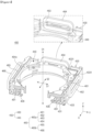
- FIG. 6 is a diagram of the lens carrier and a drive member of the camera module according to an embodiment.
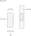
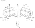
- FIG. 7A is a diagram of a first drive unit and yoke members of the camera module according to an embodiment.
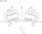
- FIG. 7B is a diagram of the first drive unit and the yoke members of the camera module according to an embodiment.
- FIG. 6 may be a view in which the camera housing 410 and the stopper 493 are omitted from the camera module 400 of FIGS. 5A and 5B .
- the camera module 400 may include the lens carrier 450, the drive member 460, and the yoke members 470. At least some of the components of the camera module 400 illustrated in FIGS. 6 , 7A , and 7B may be identical or similar to some of the components of the camera module 400 illustrated in FIGS. 4 , 5A , and 5B , and repetitive descriptions will hereinafter be omitted.
- the lens carrier 450 may include the first carrier 430 and the second carrier 440 disposed in the first carrier 430 so as to be movable.
- the second carrier 440 may be configured to move relative to the first carrier 430 in the direction of a first movement axis S1 (e.g., the y-axis direction) and the direction of a second movement axis S2 (e.g., the x-axis direction), which are substantially perpendicular to the optical axis OA, by using driving forces provided by the drive member 460.
- the first carrier 430 may include the base part 431 having the ball receiving portion 436 formed thereon and the sidewall part 433 substantially vertically extending from the base part 431.
- the ball receiving portion 436 of the first carrier 430 may be formed to face toward the second carrier 440, and the first ball 491 may be accommodated in the ball receiving portion 436.
- the sidewall part 433 of the first carrier 430 may partially face the side surface of the second carrier 440.
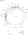
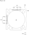
- the yoke members 470 corresponding to magnets 461 and 463 of the first drive unit 460a may be disposed on the base part 431 of the first carrier 430.
- the yoke members 470 may be disposed on one surface (e.g., the surface facing the +z-axis direction) of the base part 431 to face the first magnet 461 and the second magnet 463 in the direction of the optical axis OA.
- a first yoke member 471 may be disposed adjacent to the sidewall facing the +y-axis direction on the one surface of the base part 431 to overlap the first magnet 461 in the direction of the optical axis OA.
- a second yoke member 473 may be disposed adjacent to the sidewall facing the -x-axis direction on the one surface of the base part 431 to overlap the second magnet 463 in the direction of the optical axis OA.
- the first carrier 430 may have opening areas 4331 formed therein through which the coils 462 and 464 and the magnets 461 and 463 of the first drive unit 460a face each other.
- the sidewall of the sidewall part 433 of the first carrier 430 that faces the +y-axis direction may have the opening area 4331 through which the first coil 462 and the first magnet 461 face each other
- the sidewall facing the -x-axis direction may have the opening 4331 through which the second coil 464 and the second magnet 463 face each other.
- a third magnet 465 may be disposed on a portion of the sidewall part 433 of the first carrier 430.
- the third magnet 465 may be disposed on the sidewall of the sidewall part 433 of the first carrier 430 that faces the -y-axis direction.
- the sidewall part 433 of the first carrier 430 may partially face the sidewall (e.g., the sidewall 416 of FIGS. 5A and 5B ) of the frame 411 of the camera housing (e.g., the camera housing 410 of FIGS. 5A and 5B ), and thus the third magnet 465 may be disposed on the sidewall part 433 of the first carrier 430 to face the third coil 466 disposed on the sidewall 416 of the frame 411.
- the drive member 460 may provide driving forces to move the first carrier 430 and the second carrier 440.
- the drive member 460 may include the first drive unit 460a configured to move the second carrier 440 in directions substantially perpendicular to the optical axis OA and a second drive unit 460b configured to move the first carrier 430 in the direction of the optical axis OA.
- the first drive unit 460a may include the first magnet 461 and the first coil 462 facing each other and the second magnet 463 and the second coil 464 facing each other, and the second drive unit 460b may include the third magnet 465 and the third coil 466 facing each other.
- the coils included in the drive member 460 may be understood as being fixedly disposed on the frame (e.g., the frame 411 of FIGS. 5A and 5B ) of the camera housing 410.
- the first drive unit 460a may be configured to move the second carrier 440 in the direction of the first movement axis S1 (e.g., the +y/-y axis) and the direction of the second movement axis S2 (e.g., the +x/-x axis) that are substantially perpendicular to the optical axis OA (e.g., the +z/-z axis).
- the first movement axis S1 and the second movement axis S2 may be substantially perpendicular to each other.
- the first drive unit 460a may include the plurality of magnets 461 and 463 and the plurality of coils 462 and 464 that electromagnetically interact with each other and generate driving forces to move the second carrier 440.
- the plurality of magnets 461 and 463 may be disposed on the second carrier 440.
- the plurality of coils 462 and 464 may be disposed on the frame 411 of the camera housing 410 to face the plurality of magnets 461 and 463.
- the plurality of magnets 461 and 463 may include the first magnet 461 configured to move the second carrier 440 in the direction of the first movement axis S1 and the second magnet 463 configured to move the second carrier 440 in the direction of the second movement axis S2.
- the first magnet 461 and the second magnet 463 may be disposed to face directions substantially perpendicular to each other. For example, based on FIG.
- the first magnet 461 may face the +y-axis direction
- the second magnet 463 may face the -x-axis direction
- the plurality of coils 462 and 464 may include the first coil 462 fixedly disposed on the sidewall 416 of the frame 411 to face the first magnet 461 and the second coil 464 fixedly disposed on the sidewall 416 of the frame 411 to face the second magnet 463.
- the first drive unit 460a may include a voice coil motor (VCM) of a solenoid type.
- VCM voice coil motor
- the plurality of coils 462 and 464 of the first drive unit 460a when currents flow through the plurality of coils 462 and 464 of the first drive unit 460a in predetermined directions, magnetic fields may be generated around the plurality of coils 462 and 464 in directions determined according to the Ampere's right hand law. Attractive forces or repulsive forces may be generated between the plurality of coils 462 and 464 and the plurality of magnets 461 and 463 depending on the directions of the magnetic fields and the polarities of the magnets, and the plurality of magnets 461 and 463 may move toward or away from the plurality of relatively fixed coils 462 and 464.
- VCM voice coil motor
- the first magnet 461 may be coupled to a side surface (e.g., the side surface facing the +y-axis direction) of the second carrier 440 to face the direction of the first movement axis S1.
- the first magnet 461 may electromagnetically interact with the first coil 462.
- an attractive force or a repulsive force that acts in the direction of the first movement axis S1 may be formed between the first magnet 461 and the first coil 462 depending on the direction of a current applied to the first coil 462.
- the first magnet 461 may move relative to the first coil 462 in the direction of the first movement axis S1, and the second carrier 440 may move in the direction of the first movement axis S1 by the movement of the first magnet 461.
- the second magnet 463 may be coupled to a side surface (e.g., the side surface facing the -x-axis direction) of the second carrier 440 to face the direction of the second movement axis S2.
- the second magnet 463 may electromagnetically interact with the second coil 464.
- an attractive force or a repulsive force that acts in the direction of the second movement axis S2 may be formed between the second magnet 463 and the second coil 464 depending on the direction of a current applied to the second coil 464.
- the second magnet 463 may move relative to the second coil 464 in the direction of the second movement axis S2, and the second carrier 440 may move in the direction of the second movement axis S2 by the movement of the second magnet 463.
- the second drive unit 460b may be configured to move the first carrier 430 in the direction of the optical axis OA (e.g., the z-axis).
- the second drive unit 460b may include the third magnet 465 and the third coil 466 that electromagnetically interact with each other and generate a driving force to move the first carrier 430.
- the third magnet 465 may be disposed on the first carrier 430.
- the third coil 466 may be disposed on the frame 411 of the camera housing 410 to face the third magnet 465.
- the third coil 466 may be fixedly disposed on the sidewall 416 of the frame 411.
- the third magnet 465 may be coupled to the sidewall part 433 of the first carrier 430.
- the third magnet 465 may be coupled to the sidewall part 433 of the first carrier 430 to parallel one of the first magnet 461 or the second magnet 463.
- the third magnet 465 may be disposed in the -y-axis direction to parallel the first magnet 461.
- the position of the third magnet 465 is not limited to the illustrated example.
- the third magnet 465 may electromagnetically interact with the third coil 466.
- an electromagnetic force that acts in the direction of the optical axis OA may be formed between the third magnet 465 and the third coil 466 depending on the direction of a current applied to the third coil 466.
- the third coil 466 is fixed to the camera housing 410, the third magnet 465 may move relative to the third coil 466 in the direction of the optical axis OA, and the first carrier 430 may move in the direction of the optical axis OA by the movement of the third magnet 465.
- the third magnet 465 may have a form in which the surface facing the third coil 466 is polarized in the direction of the optical axis OA, and the electromagnetic force acting between the third magnet 465 and the third coil 466 may be understood as the Lorentz force.
- the yoke members 470 may form attractive forces with the plurality of magnets (e.g., the first magnet 461 and the third magnet 463) included in the first drive unit 460a.
- the yoke members 470 may be disposed on the base part 431 of the first carrier 430 to partially overlap the plurality of magnets 461 and 463 in the direction of the optical axis OA.
- the yoke members 470 and the plurality of magnets 461 and 463 may be spaced apart from each other by a predetermined gap, and attractive forces (e.g., magnetic attractive forces) may act between the yoke members 470 and the plurality of magnets 461 and 463.
- External forces may be applied to the second carrier 440 in a direction toward the base part 431 of the first carrier 430 by the attractive forces between the yoke members 470 and the plurality of magnets 461 and 463. Accordingly, the first ball 491 disposed between the first carrier 430 and the second carrier 440 may rotate and/or move in the state of being brought into close contact with the first carrier 430 and the second carrier 440.
- the yoke members 470 may provide a function of restraining the plurality of magnets 461 and 463 and the second carrier 440 in a predetermined range through the attractive forces between the yoke members 470 and the plurality of magnets 461 and 463.
- a movement of the second carrier 440 in the direction of the optical axis OA may be limited within a predetermined range by the attractive forces between the yoke members 470 and the plurality of magnets 461 and 463.
- the attractive forces between the yoke members 470 and the plurality of magnets 461 and 463 may act as restoring forces to restore the positions of the plurality of magnets 461 and 463.
- restoring forces to restore the plurality of magnets 461 and 463 to the initial positions before the movement may be applied to the plurality of magnets 461 and 463 by the attractive forces between the yoke members 470 and the plurality of magnets 461 and 463.
- the second carrier 440 may be restrained to the first carrier 430 through the magnetic spring structure including the yoke members 470 and the plurality of magnets 461 and 463.
- the yoke members 470 may include the first yoke member 471 corresponding to the first magnet 461 and the second yoke member 473 corresponding to the second magnet 463.
- the first yoke member 471 may be fixedly disposed on the base part 431 to face the first magnet 461 in the direction of the optical axis OA.
- the second yoke member 473 may be fixedly disposed on the base part 431 to face the second magnet 463 in the direction of the optical axis OA.
- the first yoke member 471 and the second yoke member 473 may be attached to the base part 431 or may be integrally formed with the base part 431 through an injection process, but are not limited thereto.
- the first yoke member 471 may extend in the direction of the second movement axis S2, and the second yoke member 473 may extend in the direction of the first movement axis S1.
- the first yoke member 471 may have substantially the same length as the first magnet 461, or may be longer than the first magnet 461.
- the length of the first yoke member 471 in the direction of the second movement axis S2 may be greater than, or substantially the same as, the length of the first magnet 461 in the direction of the second movement axis S2.
- the second yoke member 473 may have substantially the same length as the second magnet 463, or may be longer than the second magnet 463.
- the length of the second yoke member 473 in the direction of the first movement axis S1 may be greater than, or substantially the same as, the length of the second magnet 463 in the direction of the first movement axis S1.
- the camera module 400 may further include shielding members 494a, 494b, and 494c for shielding magnetic fields of the magnets 461, 463, and 465 included in the drive member 460.
- the shielding members 494a, 494b, and 494c may be disposed on surfaces of the magnets 461, 463, and 465.
- the shielding members 494a, 494b, and 494c may be formed of a ferromagnetic material and may be configured to shield the magnetic fields formed by the magnets 461, 463, and 465.
- the shielding members 494a, 494b, and 494c may include the first shielding member 494a corresponding to the first magnet 461, the second shielding member 494b corresponding to the second magnet 463, and the third shielding member 494c corresponding to the third magnet 465.
- the first shielding member 494a may be disposed on one surface of the first magnet 461, and the second shielding member 494b may be disposed on one surface of the second magnet 463.
- the one surface of the first magnet 461 on which the first shielding member 494a is disposed may be a surface (e.g., the surface facing the -y-axis direction) facing away from the surface of the first magnet 461 that faces the first coil 462
- the one surface of the second magnet 463 on which the second shielding member 494b is disposed may be a surface (e.g., the surface facing the +x-axis direction) facing away from the surface of the second magnet 463 that faces the second coil 464.
- the first shielding member 494a may be disposed between the first magnet 461 and the second carrier 440 such that the magnetic field formed by the first magnet 461 fails to pass through the second carrier 440.
- the second shielding member 494b may be disposed between the second magnet 463 and the second carrier 440 such that the magnetic field formed by the second magnet 463 fails to pass through the second carrier 440.
- the third shielding member 494c may be disposed on one surface of the third magnet 465.
- the one surface of the third magnet 465 on which the third shielding member 494c is disposed may be a surface (e.g., the surface facing the +y-axis direction) facing away from the surface of the third magnet 465 that faces the third coil 466.
- the third shielding member 494c may be disposed between the third magnet 465 and the second carrier 440 such that the magnetic field formed by the third magnet 465 fails to pass through the first carrier 430 (or, the second carrier 440).
- the third shielding member 494c may be disposed on the sidewall part 433 (e.g., the sidewall facing the -y-axis direction) of the first carrier 430 together with the third magnet 465 and may block the space between the inner space of the first carrier 430 and the third magnet 465.
- FIG. 8 is a plan view of the camera module according to an embodiment.
- FIG. 9 is a diagram of the second carrier and the first drive unit of the camera module according to an embodiment.
- FIG. 10A is a diagram of the first drive unit and the yoke members of the camera module according to an embodiment.
- FIG. 10B is a diagram of the first drive unit and the yoke members of the camera module according to an embodiment.
- FIGS. 8 and 9 may be views of the camera module 400 as viewed from above (e.g., the +z-axis direction).
- FIG. 8 may be a view in which the cover 413, the lens assembly 420, the stopper 493, and the coils 462, 464, and 466 are omitted.
- FIG. 9 may be a view illustrating a positional relationship between the first drive unit 460a and the second carrier 440 for an OIS operation.
- the camera module 400 may include the camera housing 410, the first carrier 430, the second carrier 440, the first drive unit 460a, the third magnet 465 (e.g., the second drive unit 460b), and the yoke members 470.
- the camera housing 410 of FIG. 8 may be referred to as a frame (e.g., the frame 411 of FIGS. 5A and 5B ).
- the frame 411 may include the sidewall 416 formed to laterally surround the first carrier 430.
- At least one second ball 492 may be disposed between the sidewall 416 and the first carrier 430.
- the second ball 492 may provide a rolling frictional force when the first carrier 430 moves relative to the frame 411 in the direction of the optical axis OA.
- the second ball 492 may at least partially make contact with the sidewall 416 and the first carrier 430.
- the first carrier 430 may be configured to move relative to the camera housing 410 in the direction of the optical axis OA.
- the second carrier 440 may be configured to move relative to the first carrier 430 and the camera housing 410 in one or more directions substantially perpendicular to the optical axis OA.
- the second carrier 440 may move together with the first carrier 430 when the first carrier 430 moves in the direction of the optical axis OA.
- the first carrier 430 may be configured to be moved in the direction of the optical axis OA by the third magnet 465.
- the third magnet 465 may be disposed on the first carrier 430, and the third coil (e.g., the third coil 466 of FIG. 6 ) corresponding to the third magnet 465 may be fixedly disposed on the sidewall 416 of the frame 411 to face the third magnet 465.
- the third magnet 465 and the third coil 466 may electromagnetically interact with each other to move the first carrier 430 in the direction of the optical axis OA.
- the second carrier 440 may include a plurality of side surfaces 445 that face directions substantially perpendicular to the optical axis OA.
- the plurality of side surfaces 445 may include a first side surface 441 and a third side surface 443 that face the direction of the first movement axis S1 and face each other and a second side surface 442 and a fourth side surface 444 that face the direction of the second movement axis S2 and face each other.
- the first side surface 441 and the third side surface 443 may extend in the direction of the second movement axis S2 by a predetermined length
- the second side surface 442 and the fourth side surface 444 may extend in the direction of the first movement axis S1 by a predetermined length.
- the first side surface 441 may face the +y-axis direction
- the second side surface 442 may face the -x-axis direction
- the third side surface 443 may face the -y-axis direction
- the fourth side surface 444 may face the +x-axis direction.
- the first side surface 441 and the third side surface 443 may be substantially perpendicular to the second side surface 442 and the fourth side surface 444.
- the second side surface 442 may extend from one end of the first side surface 441 toward one end of the third side surface 443 so as to be substantially perpendicular to the first side surface 441 and the third side surface 443, and the fourth side surface 444 may extend from an opposite end of the first side surface 441 toward an opposite end of the third side surface 443 so as to be substantially perpendicular to the first side surface 441 and the third side surface 443.
- the first drive unit 460a may be configured to move the second carrier 440 in the direction of the first movement axis S1 and the direction of the second movement axis S2 that are substantially perpendicular to the optical axis OA.
- the first movement axis S1 and the second movement axis S2 may be perpendicular to each other.
- the first drive unit 460a may include the first magnet 461 and the first coil 462 for a movement of the second carrier 440 in the direction of the first movement axis S1.
- the first drive unit 460a may include the second magnet 463 and the second coil 464 for a movement of the second carrier 440 in the direction of the second movement axis S2.
- the first magnet 461 and the second magnet 463 may be disposed to face directions perpendicular to each other.
- the first magnet 461 may be disposed on the second carrier 440 to face the direction of the first movement axis S1
- the second magnet 463 may be disposed on the second carrier 440 to face the direction of the second movement axis S2.
- the first magnet 461 may be disposed on the first side surface 441 of the second carrier 440
- the second magnet 463 may be disposed on the second side surface 442 of the second carrier 440.
- the positions of the first magnet 461 and the second magnet 463 are not limited to the illustrated embodiment.
- the first magnet 461 may be disposed on one of the first side surface 441 or the third side surface 443, and the second magnet 463 may be disposed on one of the second side surface 442 or the fourth side surface 444.
- the first coil 462 may be disposed on the frame 411 to face the first magnet 461
- the second coil 464 may be disposed on the frame 411 to face the second magnet 463.
- the first coil 462 may be fixedly disposed on the sidewall 416 of the frame 411 to overlap the first magnet 461 in the direction of the first movement axis S1
- the second coil 464 may be fixedly disposed on the sidewall 416 of the frame 411 to overlap the second magnet 463 in the direction of the second movement axis S2.
- the first magnet 461 and the first coil 462 may electromagnetically interact with each other to move the second carrier 440 in the direction of the first movement axis S1.
- the second magnet 463 and the second coil 464 may electromagnetically interact with each other to move the second carrier 440 in the direction of the second movement axis S2.
- the lens assembly e.g., the lens assembly 420 of FIG. 4
- an optical image stabilization function or, a shake correction function
- the yoke members 470 may include the first yoke member 471 corresponding to the first magnet 461 and the second yoke member 473 corresponding to the second magnet 463.
- the first yoke member 471 may be fixedly disposed on the first carrier 430 to overlap the first magnet 461 in the direction of the optical axis OA.
- the second yoke member 473 may be fixedly disposed on the first carrier 430 to overlap the second magnet 463 in the direction of the optical axis OA.
- the first yoke member 471 and the second yoke member 473 may form attractive forces with the first magnet 461 and the second magnet 463, respectively. Accordingly, the second carrier 440 may be restrained through a magnetic spring formed by the attractive force between the first magnet 461 and the first yoke member 471 and the attractive force between the second magnet 463 and the second yoke member 473. In this state, the second carrier 440 may be movable in the first carrier 430 in the direction of the first movement axis S1 and the direction of the second movement axis S2.
- the second carrier 440 may receive driving forces generated by the first drive unit 460a.
- a driving force may be applied to the second carrier 440 in the direction of the first movement axis S1 by the first magnet 461 and the first coil 462, and a driving force may be applied to the second carrier 440 in the direction of the second movement axis S2 by the second magnet 463 and the second coil 464.
- rotation R e.g., a rotary motion or a rotational component
- the rotation R may be generated by the driving forces.
- the rotation R may act as crosstalk to affect an operation of controlling a movement of the second carrier 440 and obstruct the optical image stabilization function.
- the camera module 400 may be configured to suppress the rotation R through asymmetrical shapes of the yoke members 470 or to suppress the rotation R through adjustment of the positions in which the yoke members 470 and the magnets 461 and 463 are disposed.
- the yoke members 470 may be formed in a shape for increasing restoring forces (e.g., rotational restoring forces) acting on the magnets 461 and 463.
- restoring forces e.g., rotational restoring forces
- asymmetrical shapes of the yoke members 470 for increasing the rotational restoring forces will be described.
- the positions of the yoke members 470 and the magnets 461 and 463 for increasing the restoring forces will be described below with reference to FIG. 15 .
- the rotation R of the second carrier 440 may be made about a virtual rotation axis RA parallel to the optical axis OA.
- the rotation R of the second carrier 440 may be made about the rotation axis RA in a predetermined range in opposite directions (e.g., the clockwise and counterclockwise directions based on FIG. 9 ).
- the rotation axis RA may be defined as a virtual axis extending parallel to the optical axis OA while passing through the center of a line segment LS connecting the center of the first magnet 461 and the center of the second magnet 463. For example, referring to FIGS.
- a first central axis CA1 parallel to the optical axis OA while passing through the center of the first magnet 461 and a second central axis CA2 parallel to the optical axis OA while passing through the center of the second magnet 463 may be defined.
- the line segment LS may connect the first central axis CA1 and the second central axis CA2 so as to be perpendicular to the first central axis CA1 and the second central axis CA2, and the rotation axis RA may extend parallel to the optical axis OA while passing through the center of the line segment LS.
- the line segment LS may be a line extending from one point of the first central axis CA1 toward the second central axis CA2 so as to be perpendicular to the second central axis CA2.
- the line segment LS may be perpendicular to the first central axis CA1, the second central axis CA2, and the optical axis OA.
- the first yoke member 471 when viewed in directions perpendicular to the optical axis OA, the first yoke member 471 may be disposed in a position in which the center of the first yoke member 471 overlaps the first central axis CA1 of the first magnet 461, and the second yoke member 473 may be disposed in a position in which the center of the second yoke member 473 overlaps the second central axis CA2 of the second magnet 463. Referring to FIGS.
- the first central axis CA1 when viewed in the direction of the first movement axis S1, the first central axis CA1 may pass through the center of the first magnet 461 and the center of the first yoke member 471, and when viewed in the direction of the second movement axis S2, the second central axis CA2 may pass through the center of the second magnet 463 and the center of the second yoke member 473.
- Each of the center of the first yoke member 471 and the center of the second yoke member 473 may be defined as a point that bisects the distance between the opposite outermost ends.
- the first magnet 461 and the second magnet 463 may be formed in substantially the same size or shape, and the first yoke member 471 and the second yoke member 473 may be formed in substantially the same size or shape.
- the yoke members 470 may be formed in an asymmetrically divided shape.
- Each of the first yoke member 471 and the second yoke member 473 may be formed such that at least two parts are spaced apart from each other by a predetermined gap.
- the first yoke member 471 may have an asymmetrical shape with respect to the first central axis CA1
- the second yoke member 473 may have an asymmetrical shape with respect to the second central axis CA2. Because each of the yoke members 470 is asymmetrically divided, biased magnetic forces (e.g., magnetic attractive forces) may be formed between the magnets 461 and 463 and the yoke members 470.
- the yoke members 470 may be configured such that attractive forces formed between parts relatively far away from the rotation axis RA and the magnets 461 and 463 are greater than attractive forces formed between other parts relatively close to the rotation axis RA and the magnets 461 and 463.
- the yoke members 470 may be formed such that the areas or lengths of the parts far away from the rotation axis RA are greater than the areas or lengths of the parts close to the rotation axis RA.
- each of the yoke members 470 may be asymmetrically divided into two parts.
- the first yoke member 471 may include a first part 471a and a second part 471b spaced apart from the first part 471a by a predetermined gap
- the second yoke member 473 may include a first part 473a and a second part 473b spaced apart from the first part 473a by a predetermined gap.
- the first yoke member 471 may be formed such that the second part 471b is spaced apart from the first part 471a in the direction of the second movement axis S2.
- the second yoke member 473 may be formed such that the second part 473b is spaced apart from the first part 473a in the direction of the first movement axis S1.
- the yoke members 470 may be configured such that the first parts 471a and 473a are located relatively close to the rotation axis RA and the second parts 471b and 473b are located relatively far away from the rotation axis RA.
- the first part 471a and the second part 471b of the first yoke member 471 may be sequentially disposed in a first direction 1 parallel to the second movement axis S2, and the first direction 1 may be a direction away from the second magnet 463.
- first part 473a and the second part 473b of the second yoke member 473 may be sequentially disposed in a second direction 2 parallel to the first movement axis S1, and the second direction 2 may be a direction away from the first magnet 461.
- the first yoke member 471 and the second yoke member 473 may be formed such that the areas (or, sizes) of the second parts 471b and 473b located far away from the rotation axis RA are greater than the areas (or, sizes) of the first parts 471a and 473a located close to the rotation axis RA.
- the first yoke member 471 may be formed such that the widths of the first part 471a and the second part 471b (e.g., the distances measured in the y-axis direction or the direction of the first movement axis S1) are equal to each other and the length of the second part 471b (e.g., the distance measured in the x-axis direction or the direction of the second movement axis S2) is longer than the length of the first part 471a.
- the widths of the first part 471a and the second part 471b e.g., the distances measured in the y-axis direction or the direction of the first movement axis S1
- the length of the second part 471b e.g., the distance measured in the x-axis direction or the direction of the second movement axis S2
- the second yoke member 473 may be formed such that the widths of the first part 473a and the second part 473b (e.g., the distances measured in the x-axis direction or the direction of the second movement axis S2) are equal to each other and the length of the second part 473b (e.g., the distance measured in the y-axis direction or the direction of the first movement axis S1) is longer than the length of the first part 473a. Accordingly, the second parts 471b and 473b located relatively far away from the rotation axis RA may form stronger attractive forces with the magnets 461 and 462 than the first parts 471a and 473a.
- each of the yoke members 470 may be asymmetrically divided into three parts.
- the first yoke member 471 may include a first part 471a, a second part 471b spaced apart from the first part 471a by a predetermined gap, and a third part 471c spaced apart from the second part 471b by a predetermined gap
- the second yoke member 473 may include a first part 473a, a second part 473b spaced apart from the first part 473a by a predetermined gap, and a third part 473c spaced apart from the second part 473b by a predetermined gap.
- the first yoke member 471 may be formed such that the second part 471b and the third part 471c are spaced apart from the first part 471a in the direction of the second movement axis S2.
- the second yoke member 473 may be formed such that the second part 473b and the third part 473c are spaced apart from the first part 473a in the direction of the first movement axis S1.
- the yoke members 470 may be configured such that the third parts 471c and 473c are located farther away from the rotation axis RA than the first parts 471a and 473a and the second parts 471b and 473b.
- the first part 471a, the second part 471b, and the third part 471c of the first yoke member 471 may be sequentially disposed in the first direction 1 parallel to the second movement axis S2, and the first direction 1 may be a direction away from the second magnet 463.
- first part 473a, the second part 473b, and the third part 473c of the second yoke member 473 may be sequentially disposed in the second direction 2 parallel to the first movement axis S1, and the second direction 2 may be a direction away from the first magnet 461.
- the first yoke member 471 and the second yoke member 473 may be formed such that the areas (or, sizes) of the third parts 471c and 473c located far away from the rotation axis RA are greater than the areas (or, sizes) of the first parts 471a and 473a and the second parts 471b and 473b located close to the rotation axis RA.
- the first yoke member 471 may be formed such that the first part 471a, the second part 471b, and the third part 471c have the same width and the third part 471c is longer than the first part 471a and the second part 471b.
- the second yoke member 473 may be formed such that the first part 473a, the second part 473b, and the third part 473c have the same width and the third part 473c is longer than the first part 473a and the second part 473b. Accordingly, the third parts 471c and 473c located relatively far away from the rotation axis RA may form stronger attractive forces with the magnets 461 and 463 than the first parts 471a and 473a and the second parts 471b and 473b.
- the first parts 471a and 473a and the second parts 471b and 473b may have the same area (or, length), and the areas (or, lengths) of the second parts 471b and 473b may be greater than the areas (or, lengths) of the first parts 471a and 473a.
- the camera module 400 may be configured such that relatively strong magnetic attractive forces act on the parts of the yoke members 470 located far away from the rotation axis RA. Accordingly, the camera module 400 may increase the rotational restoring forces (e.g., torques) acting on the second carrier 440, and thus may decrease the rotation R of the second carrier 440.
- relatively strong magnetic attractive forces act on the parts of the yoke members 470 located far away from the rotation axis RA. Accordingly, the camera module 400 may increase the rotational restoring forces (e.g., torques) acting on the second carrier 440, and thus may decrease the rotation R of the second carrier 440.
- FIG. 11 is a diagram of various shapes of yoke members of the camera module according to an embodiment.
- FIG. 12 is a graph depicting the magnitudes of rotational restoring forces for the various shapes of the yoke members illustrated in FIG. 11 according to an embodiment.
- FIG. 11 is a view illustrating the shapes of yoke members according to comparative example 1101, comparative example 1102, embodiment 1103, and embodiment 1104.
- FIG. 12 is a graph depicting rotational restoring forces (e.g., torques) of the yoke members according to comparative example 1101, comparative example 1102, embodiment 1103, and embodiment 1104.
- each of the yoke members 470 may be disposed on the first carrier 430.
- the yoke members 470 may include a first yoke member 471 and a second yoke member 473, and the first yoke member 471 and the second yoke member 473 may be disposed substantially perpendicular to each other.
- the yoke members 470 of comparative example 1101 may be integrally formed without being divided.
- Each of the yoke members 470 of comparative example 1102 may be divided into two parts symmetrical to each other.
- the yoke members 470 of comparative example 1102 may have a shape in which first parts 471a and 473a and second parts 471b and 473b have the same area (or, length) so as to be symmetrical to each other with respect to the center of the yoke members 470.
- the yoke members 470 of embodiment 1103 may have a shape in which first parts 471a and 473a, second parts 471b and 473b, and third parts 471c and 473c are asymmetrically divided from one another and the areas of the third parts 471c and 473c located far away from the rotation axis RA are greater than the areas of the first parts 471a and 473a and the second parts 471b and 473b.
- the yoke members 470 of embodiment 1103 may be referred to as the yoke members 470 illustrated in FIG. 10B .
- the yoke members 470 of embodiment 1104 may have a shape in which first parts 471a and 473a and second parts 471b and 473b are asymmetrically divided from each other and the areas of the second parts 471b and 473b located far away from the rotation axis RA are greater than the areas of the first parts 471a and 473a.
- the yoke members 470 of embodiment 1104 may be referred to as the yoke members 470 illustrated in FIG. 10A .
- the entire lengths L of the yoke members 470 of comparative example 1101, comparative example 1102, embodiment 1103, and embodiment 1104 may be substantially the same.
- the entire lengths L of the yoke members 470 may refer to the distances between the opposite outermost ends.
- the entire lengths L of the yoke members 470 of comparative example 1102 and embodiment 1104 may be the distances between the outer ends of the first parts 471a and 473a and the outer ends of the second parts 471b and 473b.
- the entire lengths L of the yoke members 470 of embodiment 1103 may be the distances between the outer ends of the first parts 471a and 473a and the outer ends of the third parts 471c and 473c.
- graph 1201 is a graph depicting the rotational restoring forces of the yoke members according to comparative example 1101, comparative example 1102, embodiment 1103, and embodiment 1104 and is a graph depicting rotational restoring force (unit: ⁇ Nm) versus rotation angle (unit: ° (degree)).
- the horizontal axis represents rotation angle
- the vertical axis represents rotational restoring force.
- (a) is a graph depicting the rotational restoring forces of the yoke members according to embodiment 1104,
- (b) is a graph depicting the rotational restoring forces of the yoke members according to embodiment 1103
- (c) is a graph depicting the rotational restoring forces of the yoke members according to comparative example 1102
- (d) is a graph depicting the rotational restoring forces of the yoke members according to comparative example 1101.
- the rotational restoring forces for comparative example 1101, comparative example 1102, embodiment 1103, and embodiment 1104 may be listed as in Table 1 below.
- Table 1 the rotational restoring forces indicated by the + sign and the rotational restoring forces indicated by the - sign may face opposite directions.
- Comparative example 1101 Comparative example 1102 Embodiment 1103 Embodiment 1104 -2(deg) -14.38 -19.12 -22.05 -31.13 -1(deg) -6.64 -10.26 -12.01 -16.43 0(deg) 0.47 0.63 0.70 -0.04 1(deg) 7.41 10.57 12.26 18.09 2(deg) 13.81 20.23 23.24 31.71
- the magnitudes of the rotational restoring forces in embodiment 1103 and embodiment 1104 are greater than the magnitudes of the rotational restoring forces in comparative example 1101 and comparative example 1102.
- the rotational restoring forces are increased in the order of comparative example 1101, comparative example 1102, embodiment 1103 and embodiment 1104.
- the rotational restoring forces may be increased by asymmetrically dividing the yoke members 470 and making the areas (or, lengths) of the parts far away from the rotation axis RA larger.
- FIG. 13A is a diagram of yoke members having another shape according to an embodiment.
- FIG. 13B is a graph depicting the magnitudes of rotational restoring forces for the yoke members having the other shape according to an embodiment.
- FIG. 13A is a view illustrating the shape of yoke members according to comparative example 1301.
- the yoke members 470 of comparative example 1301 may have a shape in which the first parts 471a and 473a, the second parts 471b and 473b, and the third parts 471c and 473c in the yoke members 470 of embodiment 1103 illustrated in FIG. 11 are arranged in the reverse order.
- the yoke members 470 of comparative example 1103 may be formed such that first parts 471a and 473a located close to the rotation axis RA are longer than second parts 471b and 473b and third parts 471c and 473.
- graph 1302 is a graph depicting the rotational restoring forces for embodiment 1103 and comparative example 1301 and is a graph depicting rotational restoring force (unit: ⁇ Nm) versus rotation angle (unit: ° (degree)).
- the horizontal axis represents rotation angle
- the vertical axis represents rotational restoring force.
- (a) is a graph depicting the rotational restoring forces of the yoke members according to embodiment 1103
- (b) is a graph depicting the rotational restoring forces of the yoke members according to comparative example 1301.
- the rotational restoring forces for embodiment 1103 and comparative example 1301 may be listed as in Table 2 below.
- the rotational restoring forces indicated by the + sign and the rotational restoring forces indicated by the - sign may face opposite directions.
- the magnitudes of the rotational restoring forces in embodiment 1103 are greater than the magnitudes of the rotational restoring forces in comparative example 1301.
- the rotational restoring forces may be increased by asymmetrically dividing the yoke members 470 and making the areas (or, lengths) of the parts far away from the rotation axis RA larger.
- FIG. 14A is a diagram of yoke members having another shape according to an embodiment.
- FIG. 14B is a graph depicting the magnitudes of rotational restoring forces for the yoke members having the other shape according to an embodiment.
- FIG. 14A is a view illustrating the shape of yoke members according to comparative example 1401.
- the yoke members 470 of comparative example 1401 may have a shape in which the first parts 471a and 473a and the second parts 471b and 473b in the yoke members 470 of embodiment 1104 illustrated in FIG. 11 are arranged in the reverse order.
- the yoke members 470 of comparative example 1401 may be formed such that first parts 471a and 473a located close to the rotation axis RA are longer than second parts 471b and 473b.
- graph 1402 is a graph depicting the rotational restoring forces for embodiment 1104 and comparative example 1401 and is a graph depicting rotational restoring force (unit: ⁇ Nm) versus rotation angle (unit: ° (degree)).
- the horizontal axis represents rotation angle
- the vertical axis represents rotational restoring force.
- (a) is a graph depicting the rotational restoring forces of the yoke members according to embodiment 1104, and
- (b) is a graph depicting the rotational restoring forces of the yoke members according to comparative example 1401.
- the rotational restoring forces for embodiment 1104 and comparative example 1401 may be listed as in Table 3 below.
- the rotational restoring forces indicated by the + sign and the rotational restoring forces indicated by the - sign may face opposite directions.
- Embodiment 1104 Comparative example 1401 -2(deg) -31.13 -22.90 -1(deg) -16.43 -12.60 0(deg) -0.04 -0.22 1(deg) 18.09 12.36 2(deg) 31.71 22.10
- the magnitudes of the rotational restoring forces in embodiment 1104 are greater than the magnitudes of the rotational restoring forces in comparative example 1401.
- the rotational restoring forces may be increased by asymmetrically dividing the yoke members 470 and making the areas (or, lengths) of the parts far away from the rotation axis RA larger.
- FIG. 15 is a diagram of the second carrier and the first drive unit of the camera module according to an embodiment.
- the camera module 400 may include the second carrier 440 and the first drive unit 460a.
- the second carrier 440 may include the first side surface 441 and the third side surface 443 that face the direction of the first movement axis S1 and face each other and the second side surface 442 and the fourth side surface 444 that face the direction of the second movement axis S2 and face each other.
- the first drive unit 460a may include the first magnet 461 disposed on the second carrier 440 to face the direction of the first movement axis S1, the second magnet 463 disposed on the second carrier 440 to face the direction of the second movement axis S2, the first coil 462 facing the first magnet 461, and the second coil 464 facing the second magnet 463.
- the camera module 400 may be provided in a structure in which to increase rotational restoring forces, the position of the first drive unit 460a is moved in a direction in which the rotation axis RA approaches the optical axis OA.
- a first arrangement structure 1501 may be a structure before the first drive unit 460a is moved
- a second arrangement structure 1502 may be a structure after the first drive unit 460a is moved.
- the first magnet 461 may be disposed on the first side surface 441 of the second carrier 440, and the second magnet 463 may be disposed on the second side surface 442 of the second carrier 440.
- the first central axis CA1 may be substantially parallel to the optical axis OA, and the first magnet 461 may be disposed in a position in which the first central axis CA1 overlaps the optical axis OA when viewed in the direction of the first movement axis S1.
- a first line segment L1 connecting the optical axis OA and the first central axis CA1 so as to be substantially perpendicular to the optical axis OA and the first central axis CA1 may be parallel to the first movement axis S1.
- the second central axis CA2 may be substantially parallel to the optical axis OA, and the second magnet 463 may be disposed in a position in which the second central axis CA2 overlaps the optical axis OA when viewed in the direction of the second movement axis S2.
- a second line segment L2 connecting the optical axis OA and the second central axis CA2 so as to be substantially perpendicular to the optical axis OA and the second central axis CA2 may be parallel to the second movement axis S2.
- the first line segment L1 and the second line segment L2 may be defined as lines that extend from one point on the optical axis OA toward the first central axis CA1 and the second central axis CA2 so as to be perpendicular to the optical axis OA.
- the first line segment L1 connecting the optical axis OA and the first central axis CA1 and the second line segment L2 connecting the optical axis OA and the second central axis CA2 may be perpendicular to each other.
- a first virtual circle C1 having the rotation axis RA as the center thereof and passing through the first central axis CA1 and the second central axis CA2 may be defined, and the first radius r1 of the first circle C1 may be the radius of rotation of rotational restoring forces acting on the second carrier 440.
- the second arrangement structure 1502 may be a structure in which the first magnet 461 and the second magnet 463 are moved such that the distance between the rotation axis RA and the optical axis OA is shorter than that in the first arrangement structure 1501.
- the second arrangement structure 1502 may be understood as a structure in which, based on the first arrangement structure 1501, the first magnet 461 is moved in the first direction 1 away from the second magnet 463 and the second magnet 463 is moved in the second direction 2 away from the first magnet 461.
- the first direction 1 may be a direction parallel to the second movement axis S2 and away from the second magnet 463 or the second side surface 442
- the second direction 2 may be a direction parallel to the first movement axis S1 and away from the first magnet 461 or the first side surface 441.
- the first coil 462, the second coil 464, and the yoke members e.g., the yoke members 470 of FIGS. 10A and 10B
- the first yoke member 471 in response to the movement of the first magnet 461, the first yoke member 471 may be disposed in a position in which the center thereof is aligned with the first central axis CA1 of the first magnet 461, and in response to the movement of the second magnet 463, the second yoke member 473 may be disposed in a position in which the center thereof is aligned with the second central axis CA2 of the second magnet 463.
- the first magnet 461 may be disposed in a position in which the first central axis CA1 is moved in the first direction 1 with respect to the optical axis OA without overlapping the optical axis OA when viewed in the direction of the first movement axis S1.
- the second magnet 463 may be disposed in a position in which the second central axis CA2 is moved in the second direction 2 with respect to the optical axis OA without overlapping the optical axis OA when viewed in the direction of the second movement axis S2.
- a first extension line L3 extending parallel to the first movement axis S1 from the optical axis OA and a second extension line L4 extending parallel to the second movement axis S2 from the optical axis OA may be defined.
- the first magnet 461 may be disposed in a position in which the first central axis CA1 is spaced apart from the first extension line L3 by a predetermined distance in the first direction 1
- the second magnet 463 may be disposed in a position in which the second central axis CA2 is spaced apart from the second extension line L4 by a predetermined distance in the second direction 2.
- the first extension line L3 and the second extension line L4 may extend substantially perpendicular to the optical axis OA.
- the first line segment L1 connecting the optical axis OA and the first central axis CA1 so as to be perpendicular to the optical axis OA and the first central axis CA1 may not be parallel to the first movement axis S1
- the second line segment L2 connecting the optical axis OA and the second central axis CA2 so as to be perpendicular to the optical axis OA and the second central axis CA2 may not be parallel to the second movement axis S2.
- the first line segment L1 may form a first included angle A1 in the first direction 1 with the first extension line L3 (or, the first movement axis S1).
- the second line segment L2 may form a second included angle A2 in the second direction 2 with the second extension line L4 (or, the second movement axis S2).
- the first included angle A1 and the second included angle A2 may be equal to or different from each other.
- the first line segment L1 connecting the optical axis OA and the first central axis CA1 and the second line segment L2 connecting the optical axis OA and the second central axis CA2 may form an obtuse angle.
- the included angle A3 between the first line segment L1 and the second line segment L2 may be greater than 90° and smaller than 180°.
- a second virtual circle C2 having the rotation axis RA as the center thereof and passing through the first central axis CA1 and the second central axis CA2 may be defined, and the second radius r2 of the second circle C2 may be the radius of rotation of rotational restoring forces acting on the second carrier 440.
- the second radius r2 of the second circle C2 may be greater than the first radius r1 of the first circle C1 in the first arrangement structure 1501.
- a rotational restoring force that acts on the second carrier 440 may be obtained by Equation 1 below.
- ⁇ r ⁇ F
- Equation 1 “ ⁇ ” may refer to a rotational restoring force (e.g., moment or torque), “r” may refer to a radius of rotation, and “F” may refer to a force applied to the second carrier 440 (or, the magnets 461 and 463).
- the radius of rotation may be the distance from the rotation axis RA to a point at which the force is applied. Based on Equation 1 above, the rotational restoring force may be increased as the radius of rotation is increased.
- the radius of rotation r of Equation 1 in the second arrangement structure 1502 in which the rotation axis RA is located close to the optical axis OA may be greater than that in the first arrangement structure 1501 in the case in which the yoke members 470 have the same shape.
- the radius of rotation r in the first arrangement structure 1501 may be the first radius r1 of the first circle C1
- the radius of rotation r in the second arrangement structure 1502 may be the second radius r2 of the second circle C2.
- the second radius r2 may be greater than the first radius r1, and thus the rotational restoring forces in the second arrangement structure 1502 may be greater than the rotational restoring forces in the first arrangement structure 1501.
- the first magnet 461 and the second magnet 463 may be disposed in positions in which the first line segment L1 connecting the optical axis OA and the first central axis CA1 and the second line segment L2 connecting the optical axis OA and the second central axis CA2 form an obtuse angle. Accordingly, the rotational restoring forces that act on the second carrier 440 may be increased, and thus rotation of the second carrier 440 (e.g., the rotation R of FIG. 8 ) may be decreased.
- FIG. 16A is a diagram of various arrangement structures of yoke members of the camera module according to an embodiment.
- FIG. 16B is a graph depicting the magnitudes of rotational restoring forces for the various arrangement structures of the yoke members illustrated in FIG. 16A according to an embodiment.
- FIG. 16A is a view illustrating the shapes and positions of yoke members according to comparative example 1601 and embodiment 1602.
- FIG. 16B is a graph depicting rotational restoring forces (e.g., torques) for the yoke members according to comparative example 1601 and embodiment 1602.
- the yoke members 470 may have an integral shape without being divided and may be disposed in positions corresponding to a first arrangement structure (e.g., the first arrangement structure 1501 of FIG. 15 ).
- the yoke members 470 may be disposed in positions corresponding to a second arrangement structure (e.g., the second arrangement structure 1502 of FIG. 15 ) by moving the positions of the yoke members 470 and the magnets (e.g., the first magnet 461 and the second magnet 463 of FIG. 15 ) in comparative example 1601.
- embodiment 1602 may correspond to a structure in which, based on comparative example 1601, the first yoke member 471 is moved together with the first magnet 461 in the first direction 1 by a predetermined distance and the second yoke member 473 is moved together with the second magnet 463 in the second direction 2 by a predetermined distance.
- the first central axis CA1 may be spaced apart from the optical axis OA by a first distance d1 in the first direction 1
- the second central axis CA2 may be spaced apart from the optical axis OA by a second distance d2 in the second direction 2.
- the first distance d1 and the second distance d2 may be equal to or different from each other.
- graph 1603 is a graph depicting the rotational restoring forces for comparative example 1601 and embodiment 1602 and is a graph depicting rotational restoring force (unit: ⁇ Nm) versus rotation angle (unit: ° (degree)).
- the horizontal axis represents rotation angle
- the vertical axis represents rotational restoring force.
- (a) is a graph depicting the rotational restoring forces of the yoke members according to embodiment 1602
- (b) is a graph depicting the rotational restoring forces of the yoke members according to comparative example 1601.
- the magnitudes of the rotational restoring forces in the arrangement structure of embodiment 1602 are greater than the magnitudes of the rotational restoring forces in the arrangement structure of comparative example 1601.
- the radius of rotation may be formed to be larger, and thus the rotational restoring forces may be increased.
- FIG. 17A is a diagram of various arrangement structures of yoke members of the camera module according to an embodiment.
- FIG. 17B is a graph depicting the magnitudes of rotational restoring forces for the various arrangement structures of the yoke members illustrated in FIG. 17A according to an embodiment.
- FIG. 17A is a view illustrating the shapes and positions of yoke members according to comparative example 1701 and embodiment 1702.
- FIG. 17B is a graph depicting rotational restoring forces (e.g., torques) for the yoke members according to comparative example 1701 and embodiment 1702.
- the yoke members 470 may each be divided into two parts symmetrical to each other and may be disposed in positions corresponding to a first arrangement structure (e.g., the first arrangement structure 1501 of FIG. 15 ).
- the yoke members 470 may be disposed in positions corresponding to a second arrangement structure (e.g., the second arrangement structure 1502 of FIG. 15 ) by moving the positions of the yoke members 470 and the magnets (e.g., the first magnet 461 and the second magnet 463 of FIG. 15 ) in comparative example 1701.
- embodiment 1702 may correspond to a structure in which, based on comparative example 1701, the first yoke member 471 is moved together with the first magnet 461 in the first direction 1 by a predetermined distance and the second yoke member 473 is moved together with the second magnet 463 in the second direction 2 by a predetermined distance.
- the first central axis CA1 may be spaced apart from the optical axis OA by a first distance d1 in the first direction 1
- the second central axis CA2 may be spaced apart from the optical axis OA by a second distance d2 in the second direction 2.
- the first distance d1 and the second distance d2 may be equal to or different from each other.
- graph 1703 is a graph depicting the rotational restoring forces for comparative example 1701 and embodiment 1702 and is a graph depicting rotational restoring force (unit: ⁇ Nm) versus rotation angle (unit: ° (degree)).
- the horizontal axis represents rotation angle
- the vertical axis represents rotational restoring force.
- (a) is a graph depicting the rotational restoring forces of the yoke members according to embodiment 1702
- (b) is a graph depicting the rotational restoring forces of the yoke members according to comparative example 1701.
- the rotational restoring forces for comparative example 1701 and embodiment 1702 may be listed as in Table 5 below.
- Table 5 the rotational restoring forces indicated by the + sign and the rotational restoring forces indicated by the - sign may face opposite directions.
- Comparative example 1701 Embodiment 1702 -2 (deg) -19.12 -22.48 -1 (deg) -10.26 -11.79 0 (deg) 0.63 0.36 1 (deg) 10.57 12.84 2 (deg) 20.23 22.65
- the magnitudes of the rotational restoring forces in the arrangement structure of embodiment 1702 are greater than the magnitudes of the rotational restoring forces in the arrangement structure of comparative example 1701.
- the radius of rotation may be formed to be larger, and thus the rotational restoring forces may be increased.
- FIG. 18A is a diagram of various arrangement structures of yoke members of the camera module according to an embodiment.
- FIG. 18B is a graph depicting the magnitudes of rotational restoring forces for the various arrangement structures of the yoke members illustrated in FIG. 18A according to an embodiment.
- FIG. 18A is a view illustrating the shapes and positions of yoke members according to embodiment 1801 and embodiment 1802.
- FIG. 18B is a graph depicting the rotational restoring forces (e.g., torques) for the yoke members according to embodiment 1801 and embodiment 1802.
- the yoke members 470 may each be asymmetrically divided into three parts, the areas of the third parts 471c and 473c located far away from the rotation axis RA may be greater than the areas of the first parts 471a and 473a and the second parts 471b and 473b, and the yoke members 470 may be disposed in positions corresponding to a first arrangement structure (e.g., the first arrangement structure 1501 of FIG. 15 ). In embodiment 1802, the yoke members 470 may be disposed in positions corresponding to a second arrangement structure (e.g., the second arrangement structure 1502 of FIG.
- a first arrangement structure e.g., the first arrangement structure 1501 of FIG. 15
- the yoke members 470 may be disposed in positions corresponding to a second arrangement structure (e.g., the second arrangement structure 1502 of FIG.
- embodiment 1802 may correspond to a structure in which, based on embodiment 1801, the first yoke member 471 is moved together with the first magnet 461 in the first direction 1 by a predetermined distance and the second yoke member 473 is moved together with the second magnet 463 in the second direction 2 by a predetermined distance.
- graph 1803 is a graph depicting the rotational restoring forces for embodiment 1801 and embodiment 1802 and is a graph depicting rotational restoring force (unit: ⁇ Nm) versus rotation angle (unit: ° (degree)).
- the horizontal axis represents rotation angle
- the vertical axis represents rotational restoring force.
- (a) is a graph depicting the rotational restoring forces of the yoke members according to embodiment 1802
- (b) is a graph depicting the rotational restoring forces of the yoke members according to embodiment 1801.
- Embodiment 1801 Embodiment 1802 may be listed as in Table 6 below.
- the rotational restoring forces indicated by the + sign and the rotational restoring forces indicated by the - sign may face opposite directions.
- Embodiment 1801 Embodiment 1802 -2 (deg) -22.05 -25.54 -1 (deg) -12.01 -14.27 0 (deg) 0.70 -0.01 1 (deg) 12.26 13.96 2 (deg) 23.24 25.56
- the magnitudes of the rotational restoring forces in the arrangement structure of embodiment 1802 are greater than the magnitudes of the rotational restoring forces in the arrangement structure of embodiment 1801.
- the radius of rotation may be formed to be larger, and thus the rotational restoring forces may be increased.
- FIG. 19A is a diagram of various arrangement structures of yoke members of the camera module according to an embodiment.
- FIG. 19B is a graph depicting the magnitudes of rotational restoring forces for the various arrangement structures of the yoke members illustrated in FIG. 19A according to an embodiment.
- FIG. 19A is a view illustrating the shapes and positions of yoke members according to embodiment 1901 and embodiment 1902.
- FIG. 19B is a graph depicting rotational restoring forces (e.g., torques) for the yoke members according to embodiment 1901 and embodiment 1902.
- the yoke members 470 may each be asymmetrically divided into two parts, the areas of the second parts 471b and 473b located far away from the rotation axis RA may be greater than the areas of the first parts 471a and 473a, and the yoke members 470 may be disposed in positions corresponding to a first arrangement structure (e.g., the first arrangement structure 1501 of FIG. 15 ). In embodiment 1902, the yoke members 470 may be disposed in positions corresponding to a second arrangement structure (e.g., the second arrangement structure 1502 of FIG.
- embodiment 1902 may correspond to a structure in which, based on embodiment 1901, the first yoke member 471 is moved together with the first magnet 461 in the first direction 1 by a predetermined distance and the second yoke member 473 is moved together with the second magnet 463 in the second direction 2 by a predetermined distance.
- the first central axis CA1 may be spaced apart from the optical axis OA by a first distance d1 in the first direction 1
- the second central axis CA2 may be spaced apart from the optical axis OA by a second distance d2 in the second direction 2.
- the first distance d1 and the second distance d2 may be equal to or different from each other.
- graph 1903 is a graph depicting the rotational restoring forces for embodiment 1901 and embodiment 1902 and is a graph depicting rotational restoring force (unit: ⁇ Nm) versus rotation angle (unit: ° (degree)).
- the horizontal axis represents rotation angle
- the vertical axis represents rotational restoring force.
- (a) is a graph depicting the rotational restoring forces of the yoke members according to embodiment 1902
- (b) is a graph depicting the rotational restoring forces of the yoke members according to embodiment 1901.
- the rotational restoring forces for embodiment 1901 and embodiment 1902 may be listed as in Table 7 below.
- the rotational restoring forces indicated by the + sign and the rotational restoring forces indicated by the - sign may face opposite directions.
- the magnitudes of the rotational restoring forces in the arrangement structure of embodiment 1902 are greater than the magnitudes of the rotational restoring forces in the arrangement structure of embodiment 1901.
- the radius of rotation may be formed to be larger, and thus the rotational restoring forces may be increased.
- FIG. 20A is a diagram of various arrangement structures of yoke members of the camera module according to an embodiment.
- FIG. 20B is a graph depicting the magnitudes of rotational restoring forces for the various arrangement structures of the yoke members illustrated in FIG. 20A according to an embodiment.
- FIG. 20A is a view illustrating the shapes and positions of yoke members according to comparative example 2001 and embodiment 2002.
- FIG. 20B is a graph depicting rotational restoring forces (e.g., torques) for the yoke members according to comparative example 2001 and embodiment 2002.
- the yoke members 470 may each be asymmetrically divided into three parts, the areas of the first parts 471a and 473a located close to the rotation axis RA may be greater than the areas of the second parts 471b and 473b and the third parts 471c and 473c, and the yoke members 470 may be disposed in positions corresponding to a first arrangement structure (e.g., the first arrangement structure 1501 of FIG. 15 ).
- the yoke members 470 may be disposed in positions corresponding to a second arrangement structure (e.g., the second arrangement structure 1502 of FIG.
- embodiment 2002 may correspond to a structure in which, based on comparative example 2001, the first yoke member 471 is moved together with the first magnet 461 in the first direction 1 by a predetermined distance and the second yoke member 473 is moved together with the second magnet 463 in the second direction 2 by a predetermined distance.
- the first central axis CA1 may be spaced apart from the optical axis OA by a first distance d1 in the first direction 1
- the second central axis CA2 may be spaced apart from the optical axis OA by a second distance d2 in the second direction 2.
- the first distance d1 and the second distance d2 may be equal to or different from each other.
- graph 2003 is a graph depicting the rotational restoring forces for comparative example 2001 and embodiment 2002 and is a graph depicting rotational restoring force (unit: ⁇ Nm) versus rotation angle (unit: ° (degree)).
- the horizontal axis represents rotation angle
- the vertical axis represents rotational restoring force.
- (a) is a graph depicting the rotational restoring forces of the yoke members according to embodiment 2002
- (b) is a graph depicting the rotational restoring forces of the yoke members according to comparative example 2001.
- the magnitudes of the rotational restoring forces in the arrangement structure of embodiment 2002 are greater than the magnitudes of the rotational restoring forces in the arrangement structure of comparative example 2001.
- the radius of rotation may be formed to be larger, and thus the rotational restoring forces may be increased.
- FIG. 21A is a diagram of various arrangement structures of yoke members of the camera module according to an embodiment.
- FIG. 21B is a graph depicting the magnitudes of rotational restoring forces for the various arrangement structures of the yoke members illustrated in FIG. 21A according to an embodiment.
- FIG. 21A is a view illustrating the shapes and positions of yoke members according to comparative example 2101 and embodiment 2102.
- FIG. 21B is a graph depicting rotational restoring forces (e.g., torques) for the yoke members according to comparative example 2101 and embodiment 2102.
- the yoke members 470 may each be asymmetrically divided into two parts, the areas of the first parts 471a and 473a located close to the rotation axis RA may be greater than the areas of the second parts 471b and 473b, and the yoke members 470 may be disposed in positions corresponding to a first arrangement structure (e.g., the first arrangement structure 1501 of FIG. 15 ). In embodiment 2102, the yoke members 470 may be disposed in positions corresponding to a second arrangement structure (e.g., the second arrangement structure 1502 of FIG.
- embodiment 2102 may correspond to a structure in which, based on comparative example 2101, the first yoke member 471 is moved together with the first magnet 461 in the first direction 1 by a predetermined distance and the second yoke member 473 is moved together with the second magnet 463 in the second direction 2 by a predetermined distance.
- the first central axis CA1 may be spaced apart from the optical axis OA by a first distance d1 in the first direction 1
- the second central axis CA2 may be spaced apart from the optical axis OA by a second distance d2 in the second direction (2).
- the first distance d1 and the second distance d2 may be equal to or different from each other.
- graph 2103 is a graph depicting the rotational restoring forces for comparative example 2101 and embodiment 2102 and is a graph depicting rotational restoring force (unit: ⁇ Nm) versus rotation angle (unit: ° (degree)).
- the horizontal axis represents rotation angle
- the vertical axis represents rotational restoring force.
- (a) is a graph depicting the rotational restoring forces of the yoke members according to embodiment 2102
- (b) is a graph depicting the rotational restoring forces of the yoke members according to comparative example 2101.
- the magnitudes of the rotational restoring forces in the arrangement structure of embodiment 2102 are greater than the magnitudes of the rotational restoring forces in the arrangement structure of comparative example 2101.
- the radius of rotation may be formed to be larger, and thus the rotational restoring forces may be increased.
- FIG. 22 is a graph depicting the magnitudes of rotational restoring forces for yoke members according to various embodiments.
- graph 2201 is a graph depicting the rotational restoring forces for embodiment 1602 of FIG. 16A, embodiment 1702 of FIG. 17A, embodiment 1802 of FIG. 18A, and embodiment 1902 of FIG. 19A, and is a graph depicting rotational restoring force (unit: ⁇ Nm) versus rotation angle (unit: ° (degree)).
- the horizontal axis represents rotation angle
- the vertical axis represents rotational restoring force.
- (a) is a graph depicting the rotational restoring forces according to embodiment 1902
- (b) is a graph depicting the rotational restoring forces according to embodiment 1802
- (c) is a graph depicting the rotational restoring forces according to embodiment 1702
- (d) is a graph depicting the rotational restoring forces according to embodiment 1602.
- the rotational restoring forces for embodiment 1602, embodiment 1702, embodiment 1802, and embodiment 1902 may be listed as in Table 10 below.
- the rotational restoring forces indicated by the + sign and the rotational restoring forces indicated by the - sign may face opposite directions.
- Embodiment 1602 Embodiment 1702 Embodiment 1802 Embodiment 1902 -2 (deg) -17.03 -22.48 -25.54 -36.36 -1 (deg) -8.82 -11.79 -14.27 -18.33 0 (deg) 0.16 0.36 -0.01 -0.24 1 (deg) 8.82 12.84 13.96 19.42 2 (deg) 17.25 22.65 25.56 36.23
- the magnitudes of the rotational restoring forces in embodiment 1802 and embodiment 1902 are greater than the magnitudes of the rotational restoring forces in embodiment 1602 and embodiment 1702.
- the rotational restoring forces are increased in the order of embodiment 1602, embodiment 1702, embodiment 1802, and embodiment 1902.
- the rotational restoring forces may be increased by asymmetrically dividing the yoke members 470 and making the areas (or, lengths) of the parts far away from the rotation axis RA larger as described above.
- FIG. 23A is a diagram of a first drive unit and yoke members of a camera module according to various embodiments.
- FIG. 23B is a diagram of the first drive unit and the yoke members of the camera module according to various embodiments.
- the camera module 400 may include a first magnet 461, a second magnet 463 disposed perpendicular to the first magnet 461, a first coil 462 facing the first magnet 461, a second coil 464 facing the second magnet 463, a first yoke member 471 forming an attractive force with the first magnet 461, and a second yoke member 473 forming an attractive force with the second magnet 463.
- the first yoke member 471 may include a first part 471a (e.g., the first part 471a of FIG. 10A ) and a second part 471b (e.g., the second part 471b of FIG. 10A ) that are spaced apart from each other by a predetermined gap in a first direction 1.
- the first direction CD may be a direction parallel to the direction of a second movement axis (e.g., the second movement axis S2 of FIG. 9 ) and away from the second magnet 463.
- the first yoke member 471 may be formed such that the area (or, volume) of the second part 471b is greater than the area (or, volume) of the first part 471a, and thus a rotational restoring force may increase.
- the first yoke member 471 may be formed such that the area of the second part 471b increases in the first direction 1.
- the second part 471b may be formed in a shape in which the area of the surface facing the first magnet 461 increases in the first direction 1. Accordingly, a relatively strong attractive force may be formed on a portion of the second part 471b located far away from a rotation axis (e.g., the rotation axis RA of FIG. 9 ), and thus the rotational restoring force may be further increased.
- the second yoke member 473 (e.g., the first yoke member 473 of FIG. 10A ) may include a first part 473a (e.g., the first part 473a of FIG. 10A ) and a second part 473b (e.g., the second part 473b of FIG. 10A ) that are spaced apart from each other by a predetermined gap in a second direction 2.
- the second direction 2 may be a direction parallel to the direction of a first movement axis (e.g., the first movement axis S1 of FIG. 9 ) and away from the first magnet 461.
- the second yoke member 473 may be formed such that the area (or, volume) of the second part 473b is greater than the area (or, volume) of the first part 473a, and thus a rotational restoring force may increase.
- the second yoke member 473 may be formed such that the area of the second part 473b increases in the second direction 2.
- the second part 473b may be formed in a shape in which the area of the surface facing the second magnet 463 increases in the second direction 2. Accordingly, a relatively strong attractive force may be formed on a portion of the second part 473b located far away from the rotation axis (e.g., the rotation axis RA of FIG. 9 ), and thus the rotational restoring force may be further increased.
- first yoke member 471 and the second yoke member 473 illustrated in FIGS. 23A and 23B are illustrative, and the first yoke member 471 and the second yoke member 473 are not limited to the illustrated example.
- the first yoke member 471 and the second yoke member 473 may be formed in various shapes in which the areas of the second parts 471b and 473b increase gradually or in a stepwise manner in the first direction 1 and the second direction 2 depending on the shape of a first carrier (e.g., the first carrier 430 of FIG. 11 ) and the positions in which the first yoke member 471 and the second yoke member 473 are disposed on the first carrier 430.
- a first carrier e.g., the first carrier 430 of FIG. 11
- FIG. 24A is a diagram of a first drive unit and yoke members of a camera module according to various embodiments.
- FIG. 24B is a diagram of the first drive unit and the yoke members of the camera module according to various embodiments.
- the camera module 400 may include a first magnet 461, a second magnet 463 disposed perpendicular to the first magnet 461, a first coil 462 facing the first magnet 461, a second coil 464 facing the second magnet 463, a first yoke member 471 forming an attractive force with the first magnet 461, and a second yoke member 473 forming an attractive force with the second magnet 463.
- the first yoke member 471 may include a first part 471a (e.g., the first part 471a of FIG. 10B ), a second part 471b (e.g., the second part 471b of FIG. 10B ), and a third part 471c (e.g., the third part 471c of FIG. 10B ) that are spaced apart from each other by a predetermined gap in a first direction 1.
- the first direction 1 may be a direction parallel to the direction of a second movement axis (e.g., the second movement axis S2 of FIG. 9 ) and away from the second magnet 463.
- the first yoke member 471 may be formed such that the area (or, volume) of the third part 471c is greater than the areas (or, volumes) of the first part 471a and the second part 471b, and thus a rotational restoring force may increase.
- the first yoke member 471 may be formed such that the area of the third part 471c increases in the first direction 1.
- the third part 471c may be formed in a shape in which the area of the surface facing the first magnet 461 increases in the first direction 1. Accordingly, a relatively strong attractive force may be formed on a portion of the third part 471c located far away from a rotation axis (e.g., the rotation axis RA of FIG. 9 ), and thus the rotational restoring force may be further increased.
- the second yoke member 473 may include a first part 473a (e.g., the first part 473a of FIG. 10B ), a second part 473b (e.g., the second part 473b of FIG. 10B ), and a third part 473c (e.g., the third part 473c of FIG. 10B ) that are spaced apart from each other by a predetermined gap in a second direction 2.
- the second direction 2 may be a direction parallel to the direction of a first movement axis (e.g., the first movement axis S1 ofFIG. 9) and away from the first magnet 461.
- the second yoke member 473 may be formed such that the area (or, volume) of the third part 473c is greater than the areas (or, volumes) of the first part 473a and the second part 473b, and thus a rotational restoring force may increase.
- the second yoke member 473 may be formed such that the area of the third part 473c increases in the second direction 2.
- the third part 473c may be formed in a shape in which the area of the surface facing the second magnet 463 increases in the second direction 2. Accordingly, a relatively strong attractive force may be formed on a portion of the third part 473c located far away from the rotation axis (e.g., the rotation axis RA of FIG. 9 ), and thus the rotational restoring force may be further increased.
- first yoke member 471 and the second yoke member 473 illustrated in FIGS. 24A and 24B are illustrative, and the first yoke member 471 and the second yoke member 473 are not limited to the illustrated example.
- the first yoke member 471 and the second yoke member 473 may be formed in various shapes in which the areas of the third parts 471c and 473c increase gradually or in a stepwise manner in the first direction 1 and the second direction (2) depending on the shape of a first carrier (e.g., the first carrier 430 of FIG. 11 ) and the positions in which the first yoke member 471 and the second yoke member 473 are disposed on the first carrier 430.
- a first carrier e.g., the first carrier 430 of FIG. 11
- a camera module 400 may include a camera housing 410, a first carrier 430 disposed in the camera housing so as to be movable, a second carrier 440 that is at least partially disposed in the first carrier and that has a lens 421 coupled thereto and moves relative to the first carrier in at least one direction perpendicular to an optical axis OA of the lens, a plurality of magnets 461 and 463 that are disposed on the second carrier and that include a first magnet 461 and a second magnet 463 that face directions perpendicular to each other, and a plurality of yoke members 470 that are disposed on the first carrier and that form magnetic attractions with the plurality of magnets, the plurality of yoke members including a first yoke member 471 and a second yoke member 473 that face the first magnet and the second magnet, respectively.
- the first yoke member may include a first part 471a and a second part 471b spaced apart from each other in a lengthwise direction of the first magnet
- the second yoke member may include a first part 473a and a second part 473b spaced apart from each other in a lengthwise direction of the second magnet
- the second parts may be longer than the first parts or may have a larger area than the first parts.
- the first yoke member may be disposed such that the first part is located closer to the second magnet than the second part
- the second yoke member may be disposed such that the first part is located closer to the first magnet than the second part.
- the first yoke member may be configured such that the second part forms larger magnetic attraction with the first magnet than the first part
- the second yoke member may be configured such that the second part forms larger magnetic attraction with the second magnet than the first part
- the camera module may further include a first coil 462 that faces the first magnet and a second coil 464 that faces the second magnet.
- the first magnet and the first coil may be configured to move the second carrier in a direction of a first movement axis S1 perpendicular to the optical axis through electromagnetic interaction.
- the second magnet and the second coil may be configured to move the second carrier in a direction of a second movement axis S2 perpendicular to the optical axis and the first movement axis through electromagnetic interaction.
- the plurality of magnets may be disposed such that the first magnet faces the direction of the first movement axis and the second magnet faces the direction of the second movement axis.
- the first part and the second part of the first yoke member may be sequentially disposed in a first direction 1, and the first direction may be a direction parallel to the second movement axis and away from the second magnet.
- the first part and the second part of the second yoke member may be sequentially disposed in a second direction (2), and the second direction may be a direction parallel to the first movement axis and away from the first magnet.
- the first magnet and the first coil may form a driving force facing the second direction or a direction opposite to the second direction depending on a direction of a current applied to the first coil
- the second magnet and the second coil may form a driving force facing the first direction or a direction opposite to the first direction depending on a direction of a current applied to the second coil
- the first yoke member may further include a third part 471b disposed between the first part 471a and the second part 471c of the first yoke member
- the second yoke member may further include a third part 473b disposed between the first part 473a and the second part 473c of the second yoke member.
- the third parts may be shorter than the second parts or may have a smaller area than the second parts.
- first part, the third part, and the second part of the first yoke member may be sequentially disposed in the first direction
- the first part, the third part, and the second part of the second yoke member may be sequentially disposed in the second direction
- the first yoke member may be configured such that the second part forms stronger magnetic attraction with the first magnet than the first part and the third part, and the second yoke member may be configured such that the second part forms stronger magnetic attraction with the second magnet than the first part and the third part.
- a first central axis CA1 and a second central axis CA2 parallel to the optical axis may be defined in the first magnet and the second magnet, respectively.
- the first yoke member may be disposed in a position in which the center of the first yoke member overlaps the first central axis when viewed in the direction of the first movement axis
- the second yoke member may be disposed in a position in which the center of the second yoke member overlaps the second central axis when viewed in the direction of the second movement axis.
- a rotation axis RA may be defined to extend parallel to the optical axis and to pass through the center of a line segment LS connecting the first central axis and the second central axis so as to be perpendicular to the first central axis and the second central axis, and the plurality of yoke members may be configured such that the second parts are located farther away from the rotation axis than the first parts.
- the first magnet and the first yoke member may be disposed in a position in which the first central axis is spaced apart from the optical axis by a first distance d1 in the first direction when viewed in the direction of the first movement axis.
- the second magnet and the second yoke member may be disposed in a position in which the second central axis is spaced apart from the optical axis by a second distance d2 in the second direction when viewed in the direction of the second movement axis.
- a first line segment L1 connecting the optical axis and the first central axis and a second line segment L2 connecting the optical axis and the second central axis may be defined, and an included angle A3 formed by the first line segment and the second line segment may be an obtuse angle.
- the plurality of magnets may be disposed such that the first magnet faces the direction of the second movement axis and the second magnet faces the direction of the first movement axis.
- the first part and the second part of the first yoke member may be sequentially disposed in a first direction, and the first direction may be a direction parallel to the first movement axis and away from the second magnet.
- the first part and the second part of the second yoke member may be sequentially disposed in a second direction, and the second direction may be a direction parallel to the second movement axis and away from the first magnet.
- the first magnet and the first coil may form a driving force facing the first direction or a direction opposite to the first direction depending on a direction of a current applied to the first coil
- the second magnet and the second coil may form a driving force facing the second direction or a direction opposite to the second direction depending on a direction of a current applied to the second coil
- a camera module 400 may include a camera housing 410, a first carrier 430 disposed in the camera housing so as to be movable, a second carrier 440 that is at least partially disposed in the first carrier and that has a lens 421 coupled thereto and moves relative to the first carrier in a direction perpendicular to an optical axis OA of the lens, a first magnet 461 that is disposed on the second carrier and that moves the second carrier in a direction of a first movement axis S 1 perpendicular to the optical axis, a second magnet 463 that is disposed on the second carrier and that moves the second carrier in a direction of a second movement axis S2 perpendicular to the optical axis and the first movement axis, a first yoke member 471 that is disposed on the first carrier and that forms magnetic attraction with the first magnet, and a second yoke member 473 that is disposed on the first carrier and that forms magnetic attraction with the second magnet.
- a first central axis CA1 and a second central axis CA2 parallel to the optical axis may be defined in the first magnet and the second magnet, respectively.
- a first line segment L1 connecting the optical axis and the first central axis and a second line segment L2 connecting the optical axis and the second central axis may be defined, and an included angle A3 formed by the first line segment and the second line segment may be an obtuse angle.
- a first extension line L3 extending from the optical axis in a direction parallel to the first movement axis and a second extension line L4 extending from the optical axis in a direction parallel to the second movement axis may be defined.
- the first line segment may form a first included angle A1 with the first extension line in a direction away from the second magnet
- the second line segment may form a second included angle A2 with the second extension line in a direction away from the first magnet.
- the first magnet may be disposed such that opposite surfaces thereof face the direction of the first movement axis
- the second magnet may be disposed such that opposite surfaces thereof face the direction of the second movement axis.
- the first yoke member may be disposed in a position in which the center of the first yoke member overlaps the first central axis when viewed in the direction of the first movement axis
- the second yoke member may be disposed in a position in which the center of the second yoke member overlaps the second central axis when viewed in the direction of the second movement axis.
- the first magnet and the first yoke member may be disposed in a position in which the first central axis is spaced apart from the optical axis by a first distance d1 in a first direction 1 when viewed in the direction of the first movement axis.
- the first direction may be a direction parallel to the second movement axis and away from the second magnet.
- the second magnet and the second yoke member may be disposed in a position in which the second central axis is spaced apart from the optical axis by a second distance d2 in a second direction (2) when viewed in the direction of the second movement axis.
- the second direction may be a direction parallel to the first movement axis and away from the first magnet.
- the electronic device may be one of various types of electronic devices.
- the electronic devices may include, for example, a portable communication device (e.g., a smartphone), a computer device, a portable multimedia device, a portable medical device, a camera, a wearable device, or a home appliance. According to an embodiment of the disclosure, the electronic devices are not limited to those described above.
- each of such phrases as “A or B,” “at least one of A and B,” “at least one of A or B,” “A, B, or C,” “at least one of A, B, and C,” and “at least one of A, B, or C,” may include any one of, or all possible combinations of the items enumerated together in a corresponding one of the phrases.
- such terms as “1st” and “2nd,” or “first” and “second” may be used to simply distinguish a corresponding component from another, and does not limit the components in other aspect (e.g., importance or order).
- an element e.g., a first element
- the element may be coupled with the other element directly (e.g., wiredly), wirelessly, or via a third element.
- module may include a unit implemented in hardware, software, or firmware, and may interchangeably be used with other terms, for example, “logic,” “logic block,” “part,” or “circuitry”.
- a module may be a single integral component, or a minimum unit or part thereof, adapted to perform one or more functions.
- the module may be implemented in a form of an application-specific integrated circuit (ASIC).
- ASIC application-specific integrated circuit
- Various embodiments as set forth herein may be implemented as software (e.g., the program 140) including one or more instructions that are stored in a storage medium (e.g., internal memory 136 or external memory 138) that is readable by a machine (e.g., the electronic device 101).
- a processor e.g., the processor 120
- the machine e.g., the electronic device 101
- the one or more instructions may include a code generated by a complier or a code executable by an interpreter.
- the machine-readable storage medium may be provided in the form of a non-transitory storage medium.
- non-transitory simply means that the storage medium is a tangible device, and does not include a signal (e.g., an electromagnetic wave), but this term does not differentiate between where data is semi-permanently stored in the storage medium and where the data is temporarily stored in the storage medium.
- a method may be included and provided in a computer program product.
- the computer program product may be traded as a product between a seller and a buyer.
- the computer program product may be distributed in the form of a machine-readable storage medium (e.g., compact disc read only memory (CD-ROM)), or be distributed (e.g., downloaded or uploaded) online via an application store (e.g., PlayStoreTM), or between two user devices (e.g., smart phones) directly. If distributed online, at least part of the computer program product may be temporarily generated or at least temporarily stored in the machine-readable storage medium, such as memory of the manufacturer's server, a server of the application store, or a relay server.
- CD-ROM compact disc read only memory
- an application store e.g., PlayStoreTM
- two user devices e.g., smart phones
- each component e.g., a module or a program of the above-described components may include a single entity or multiple entities, and some of the multiple entities may be separately disposed in different components. According to various embodiments, one or more of the above-described components may be omitted, or one or more other components may be added. Alternatively or additionally, a plurality of components (e.g., modules or programs) may be integrated into a single component. In such a case, according to various embodiments, the integrated component may still perform one or more functions of each of the plurality of components in the same or similar manner as they are performed by a corresponding one of the plurality of components before the integration.
- operations performed by the module, the program, or another component may be carried out sequentially, in parallel, repeatedly, or heuristically, or one or more of the operations may be executed in a different order or omitted, or one or more other operations may be added.
Landscapes
- Engineering & Computer Science (AREA)
- Multimedia (AREA)
- Signal Processing (AREA)
- Physics & Mathematics (AREA)
- General Physics & Mathematics (AREA)
- Power Engineering (AREA)
- Studio Devices (AREA)
Applications Claiming Priority (3)
| Application Number | Priority Date | Filing Date | Title |
|---|---|---|---|
| KR20210139412 | 2021-10-19 | ||
| KR1020210184864A KR20230055899A (ko) | 2021-10-19 | 2021-12-22 | 카메라 모듈 및 이를 포함하는 전자 장치 |
| PCT/KR2022/014874 WO2023068602A1 (ko) | 2021-10-19 | 2022-10-04 | 카메라 모듈 및 이를 포함하는 전자 장치 |
Publications (2)
| Publication Number | Publication Date |
|---|---|
| EP4404579A1 true EP4404579A1 (de) | 2024-07-24 |
| EP4404579A4 EP4404579A4 (de) | 2025-02-19 |
Family
ID=85982478
Family Applications (1)
| Application Number | Title | Priority Date | Filing Date |
|---|---|---|---|
| EP22883826.4A Pending EP4404579A4 (de) | 2021-10-19 | 2022-10-04 | Kameramodul und elektronische vorrichtung damit |
Country Status (2)
| Country | Link |
|---|---|
| US (1) | US12028614B2 (de) |
| EP (1) | EP4404579A4 (de) |
Family Cites Families (25)
| Publication number | Priority date | Publication date | Assignee | Title |
|---|---|---|---|---|
| KR20110008714U (ko) | 2010-03-05 | 2011-09-15 | 자화전자(주) | 렌즈 초점 조절장치 |
| KR101571037B1 (ko) | 2014-01-15 | 2015-11-23 | 자화전자(주) | 카메라 렌즈 모듈 |
| WO2015060637A1 (ko) * | 2013-10-25 | 2015-04-30 | 자화전자(주) | 카메라 렌즈 모듈 |
| KR101725442B1 (ko) | 2014-03-07 | 2017-04-11 | 자화전자(주) | 카메라 렌즈 모듈 |
| US9618770B2 (en) * | 2014-04-11 | 2017-04-11 | Samsung Electro-Mechanics Co., Ltd. | Camera module with function of auto-focus and image stabilize |
| US9955077B2 (en) | 2014-06-20 | 2018-04-24 | Samsung Electro-Mechanics Co., Ltd. | Camera module |
| KR102140296B1 (ko) | 2015-11-13 | 2020-07-31 | 삼성전기주식회사 | 렌즈 구동 장치 및 이를 포함하는 카메라 모듈 |
| KR20170141523A (ko) * | 2016-06-15 | 2017-12-26 | 자화전자(주) | 일체형 요크가 구비된 ois 액추에이터 |
| KR101792441B1 (ko) | 2016-12-06 | 2017-10-31 | 삼성전기주식회사 | 카메라 모듈 |
| JP6846531B2 (ja) | 2017-09-27 | 2021-03-24 | 富士フイルム株式会社 | 像ぶれ補正装置及び撮像装置 |
| KR102457389B1 (ko) * | 2017-11-28 | 2022-10-21 | 삼성전기주식회사 | 카메라 모듈 |
| JP2019113638A (ja) * | 2017-12-22 | 2019-07-11 | シーエム・テクノロジー株式会社 | レンズ駆動装置 |
| KR20200004490A (ko) | 2018-07-04 | 2020-01-14 | 자화전자(주) | 증강된 홀딩력을 가지는 구동장치 및 이에 구비되는 홀딩 요크 |
| KR102273899B1 (ko) | 2019-04-01 | 2021-07-06 | 삼성전기주식회사 | 카메라 모듈 |
| US11513308B2 (en) | 2019-04-01 | 2022-11-29 | Samsung Electro-Mechanics Co., Ltd. | Camera module |
| KR102937627B1 (ko) | 2019-10-02 | 2026-03-11 | 엘지이노텍 주식회사 | 렌즈 구동 장치, 이를 포함하는 카메라 모듈 및 광학 기기 |
| US11733538B2 (en) * | 2019-12-10 | 2023-08-22 | Samsung Electro-Mechanics Co., Ltd. | Camera module |
| KR102272591B1 (ko) * | 2019-12-10 | 2021-07-05 | 삼성전기주식회사 | 카메라 모듈 |
| KR20220035622A (ko) * | 2020-09-14 | 2022-03-22 | 엘지이노텍 주식회사 | 렌즈구동장치, 카메라 모듈 및 광학기기 |
| KR20220089353A (ko) * | 2020-12-21 | 2022-06-28 | 삼성전자주식회사 | 카메라 모듈 및 이를 포함하는 전자 장치 |
| KR102579632B1 (ko) | 2021-02-09 | 2023-09-19 | 삼성전기주식회사 | 카메라 모듈 |
| EP4261609A4 (de) * | 2021-02-23 | 2024-06-05 | Samsung Electronics Co., Ltd. | Kameramodul und elektronische vorrichtung damit |
| US20230188851A1 (en) * | 2021-12-13 | 2023-06-15 | Samsung Electro-Mechanics Co., Ltd. | Actuator for optical image stabilization and camera module including the same |
| CN116263552A (zh) * | 2021-12-13 | 2023-06-16 | 三星电机株式会社 | 相机模块 |
| KR102803427B1 (ko) * | 2022-06-10 | 2025-05-07 | 삼성전기주식회사 | 흔들림 보정용 액추에이터 및 이를 포함하는 카메라 모듈 |
-
2022
- 2022-10-04 EP EP22883826.4A patent/EP4404579A4/de active Pending
- 2022-10-19 US US17/969,354 patent/US12028614B2/en active Active
Also Published As
| Publication number | Publication date |
|---|---|
| US12028614B2 (en) | 2024-07-02 |
| US20230117477A1 (en) | 2023-04-20 |
| EP4404579A4 (de) | 2025-02-19 |
Similar Documents
| Publication | Publication Date | Title |
|---|---|---|
| US12513378B2 (en) | Camera module and electronic device including the same | |
| US11805305B2 (en) | Camera module including a lens that rotates and moves about at least two axes and electronic device including the same | |
| US12510805B2 (en) | Camera module and electronic device including the same | |
| US12219232B2 (en) | Camera module and electronic device including the same | |
| EP4059211B1 (de) | Kameramodul und elektronische vorrichtung damit | |
| US12149829B2 (en) | Camera module with a camera housing, a lens assembly and an optical image stabilizer and electronic device including the same | |
| US12399377B2 (en) | Camera module including image stabilization assembly and electronic device including the camera module | |
| KR102920632B1 (ko) | 이미지 안정화 어셈블리, 카메라 모듈 및 이를 포함하는 전자 장치 | |
| KR20230055899A (ko) | 카메라 모듈 및 이를 포함하는 전자 장치 | |
| US12607899B2 (en) | Camera module and electronic device comprising same | |
| US20240223900A1 (en) | Camera module and electronic device comprising same | |
| EP4336254A1 (de) | Kameramodul und elektronische vorrichtung damit | |
| EP4310588A1 (de) | Bildstabilisator und elektronische vorrichtung damit | |
| US12028614B2 (en) | Camera module and electronic device including the same | |
| KR20240058731A (ko) | 이미지 스태빌라이저 및 이를 포함하는 전자 장치 | |
| CN116940892A (zh) | 相机模块及包括该相机模块的电子装置 | |
| EP4290307B1 (de) | Kameramodul und elektronische vorrichtung damit | |
| US20260086441A1 (en) | Camera module and electronic device comprising same | |
| EP4738001A1 (de) | Elektronische vorrichtung mit kameramodul | |
| US20250370216A1 (en) | Camera module including actuator | |
| EP4726468A1 (de) | Kameramodul und elektronische vorrichtung mit kameramodul | |
| CN118077212A (zh) | 相机模块和包括该相机模块的电子装置 |
Legal Events
| Date | Code | Title | Description |
|---|---|---|---|
| STAA | Information on the status of an ep patent application or granted ep patent |
Free format text: STATUS: THE INTERNATIONAL PUBLICATION HAS BEEN MADE |
|
| PUAI | Public reference made under article 153(3) epc to a published international application that has entered the european phase |
Free format text: ORIGINAL CODE: 0009012 |
|
| STAA | Information on the status of an ep patent application or granted ep patent |
Free format text: STATUS: REQUEST FOR EXAMINATION WAS MADE |
|
| 17P | Request for examination filed |
Effective date: 20240419 |
|
| AK | Designated contracting states |
Kind code of ref document: A1 Designated state(s): AL AT BE BG CH CY CZ DE DK EE ES FI FR GB GR HR HU IE IS IT LI LT LU LV MC ME MK MT NL NO PL PT RO RS SE SI SK SM TR |
|
| DAV | Request for validation of the european patent (deleted) | ||
| DAX | Request for extension of the european patent (deleted) | ||
| A4 | Supplementary search report drawn up and despatched |
Effective date: 20250121 |
|
| RIC1 | Information provided on ipc code assigned before grant |
Ipc: H02K 33/18 20060101ALI20250115BHEP Ipc: G03B 17/12 20210101ALI20250115BHEP Ipc: G03B 5/00 20210101ALI20250115BHEP Ipc: H04N 23/00 20230101ALI20250115BHEP Ipc: H04N 23/60 20230101AFI20250115BHEP |
|
| STAA | Information on the status of an ep patent application or granted ep patent |
Free format text: STATUS: EXAMINATION IS IN PROGRESS |
|
| 17Q | First examination report despatched |
Effective date: 20260121 |