EP4403364A1 - Inkjet head and inkjet printer - Google Patents
Inkjet head and inkjet printer Download PDFInfo
- Publication number
- EP4403364A1 EP4403364A1 EP23205891.7A EP23205891A EP4403364A1 EP 4403364 A1 EP4403364 A1 EP 4403364A1 EP 23205891 A EP23205891 A EP 23205891A EP 4403364 A1 EP4403364 A1 EP 4403364A1
- Authority
- EP
- European Patent Office
- Prior art keywords
- power supply
- supply voltage
- input terminal
- driver
- circuit
- Prior art date
- Legal status (The legal status is an assumption and is not a legal conclusion. Google has not performed a legal analysis and makes no representation as to the accuracy of the status listed.)
- Pending
Links
Images





Classifications
-
- B—PERFORMING OPERATIONS; TRANSPORTING
- B41—PRINTING; LINING MACHINES; TYPEWRITERS; STAMPS
- B41J—TYPEWRITERS; SELECTIVE PRINTING MECHANISMS, i.e. MECHANISMS PRINTING OTHERWISE THAN FROM A FORME; CORRECTION OF TYPOGRAPHICAL ERRORS
- B41J2/00—Typewriters or selective printing mechanisms characterised by the printing or marking process for which they are designed
- B41J2/005—Typewriters or selective printing mechanisms characterised by the printing or marking process for which they are designed characterised by bringing liquid or particles selectively into contact with a printing material
- B41J2/01—Ink jet
- B41J2/015—Ink jet characterised by the jet generation process
- B41J2/04—Ink jet characterised by the jet generation process generating single droplets or particles on demand
- B41J2/045—Ink jet characterised by the jet generation process generating single droplets or particles on demand by pressure, e.g. electromechanical transducers
- B41J2/04501—Control methods or devices therefor, e.g. driver circuits, control circuits
- B41J2/04541—Specific driving circuit
-
- B—PERFORMING OPERATIONS; TRANSPORTING
- B41—PRINTING; LINING MACHINES; TYPEWRITERS; STAMPS
- B41J—TYPEWRITERS; SELECTIVE PRINTING MECHANISMS, i.e. MECHANISMS PRINTING OTHERWISE THAN FROM A FORME; CORRECTION OF TYPOGRAPHICAL ERRORS
- B41J2/00—Typewriters or selective printing mechanisms characterised by the printing or marking process for which they are designed
- B41J2/005—Typewriters or selective printing mechanisms characterised by the printing or marking process for which they are designed characterised by bringing liquid or particles selectively into contact with a printing material
- B41J2/01—Ink jet
- B41J2/135—Nozzles
-
- B—PERFORMING OPERATIONS; TRANSPORTING
- B41—PRINTING; LINING MACHINES; TYPEWRITERS; STAMPS
- B41J—TYPEWRITERS; SELECTIVE PRINTING MECHANISMS, i.e. MECHANISMS PRINTING OTHERWISE THAN FROM A FORME; CORRECTION OF TYPOGRAPHICAL ERRORS
- B41J2/00—Typewriters or selective printing mechanisms characterised by the printing or marking process for which they are designed
- B41J2/005—Typewriters or selective printing mechanisms characterised by the printing or marking process for which they are designed characterised by bringing liquid or particles selectively into contact with a printing material
- B41J2/01—Ink jet
-
- B—PERFORMING OPERATIONS; TRANSPORTING
- B41—PRINTING; LINING MACHINES; TYPEWRITERS; STAMPS
- B41J—TYPEWRITERS; SELECTIVE PRINTING MECHANISMS, i.e. MECHANISMS PRINTING OTHERWISE THAN FROM A FORME; CORRECTION OF TYPOGRAPHICAL ERRORS
- B41J2/00—Typewriters or selective printing mechanisms characterised by the printing or marking process for which they are designed
- B41J2/005—Typewriters or selective printing mechanisms characterised by the printing or marking process for which they are designed characterised by bringing liquid or particles selectively into contact with a printing material
- B41J2/01—Ink jet
- B41J2/015—Ink jet characterised by the jet generation process
- B41J2/04—Ink jet characterised by the jet generation process generating single droplets or particles on demand
- B41J2/045—Ink jet characterised by the jet generation process generating single droplets or particles on demand by pressure, e.g. electromechanical transducers
- B41J2/04501—Control methods or devices therefor, e.g. driver circuits, control circuits
-
- B—PERFORMING OPERATIONS; TRANSPORTING
- B41—PRINTING; LINING MACHINES; TYPEWRITERS; STAMPS
- B41J—TYPEWRITERS; SELECTIVE PRINTING MECHANISMS, i.e. MECHANISMS PRINTING OTHERWISE THAN FROM A FORME; CORRECTION OF TYPOGRAPHICAL ERRORS
- B41J2/00—Typewriters or selective printing mechanisms characterised by the printing or marking process for which they are designed
- B41J2/005—Typewriters or selective printing mechanisms characterised by the printing or marking process for which they are designed characterised by bringing liquid or particles selectively into contact with a printing material
- B41J2/01—Ink jet
- B41J2/015—Ink jet characterised by the jet generation process
- B41J2/04—Ink jet characterised by the jet generation process generating single droplets or particles on demand
- B41J2/045—Ink jet characterised by the jet generation process generating single droplets or particles on demand by pressure, e.g. electromechanical transducers
- B41J2/04501—Control methods or devices therefor, e.g. driver circuits, control circuits
- B41J2/04548—Details of power line section of control circuit
-
- B—PERFORMING OPERATIONS; TRANSPORTING
- B41—PRINTING; LINING MACHINES; TYPEWRITERS; STAMPS
- B41J—TYPEWRITERS; SELECTIVE PRINTING MECHANISMS, i.e. MECHANISMS PRINTING OTHERWISE THAN FROM A FORME; CORRECTION OF TYPOGRAPHICAL ERRORS
- B41J2/00—Typewriters or selective printing mechanisms characterised by the printing or marking process for which they are designed
- B41J2/005—Typewriters or selective printing mechanisms characterised by the printing or marking process for which they are designed characterised by bringing liquid or particles selectively into contact with a printing material
- B41J2/01—Ink jet
- B41J2/015—Ink jet characterised by the jet generation process
- B41J2/04—Ink jet characterised by the jet generation process generating single droplets or particles on demand
- B41J2/045—Ink jet characterised by the jet generation process generating single droplets or particles on demand by pressure, e.g. electromechanical transducers
- B41J2/04501—Control methods or devices therefor, e.g. driver circuits, control circuits
- B41J2/0455—Details of switching sections of circuit, e.g. transistors
-
- B—PERFORMING OPERATIONS; TRANSPORTING
- B41—PRINTING; LINING MACHINES; TYPEWRITERS; STAMPS
- B41J—TYPEWRITERS; SELECTIVE PRINTING MECHANISMS, i.e. MECHANISMS PRINTING OTHERWISE THAN FROM A FORME; CORRECTION OF TYPOGRAPHICAL ERRORS
- B41J2/00—Typewriters or selective printing mechanisms characterised by the printing or marking process for which they are designed
- B41J2/005—Typewriters or selective printing mechanisms characterised by the printing or marking process for which they are designed characterised by bringing liquid or particles selectively into contact with a printing material
- B41J2/01—Ink jet
- B41J2/015—Ink jet characterised by the jet generation process
- B41J2/04—Ink jet characterised by the jet generation process generating single droplets or particles on demand
- B41J2/045—Ink jet characterised by the jet generation process generating single droplets or particles on demand by pressure, e.g. electromechanical transducers
- B41J2/04501—Control methods or devices therefor, e.g. driver circuits, control circuits
- B41J2/04581—Control methods or devices therefor, e.g. driver circuits, control circuits controlling heads based on piezoelectric elements
-
- B—PERFORMING OPERATIONS; TRANSPORTING
- B41—PRINTING; LINING MACHINES; TYPEWRITERS; STAMPS
- B41J—TYPEWRITERS; SELECTIVE PRINTING MECHANISMS, i.e. MECHANISMS PRINTING OTHERWISE THAN FROM A FORME; CORRECTION OF TYPOGRAPHICAL ERRORS
- B41J29/00—Details of, or accessories for, typewriters or selective printing mechanisms not otherwise provided for
- B41J29/38—Drives, motors, controls or automatic cut-off devices for the entire printing mechanism
- B41J29/393—Devices for controlling or analysing the entire machine ; Controlling or analysing mechanical parameters involving printing of test patterns
Definitions
- Embodiments described herein relate generally to an inkjet head and an inkjet printer.
- the inkjet printer includes, for example, an inkjet head and a head controller that controls the inkjet head.
- the inkjet head includes an actuator for ejecting ink and a driver IC for driving the actuator under the control of the head controller.
- the head controller supplies a plurality of power supply voltages to the driver IC of the inkjet head.
- the head controller inputs and interrupts the plurality of power supply voltages based on a predetermined order. With this configuration, the head controller prevents a through-current from flowing in the driver IC.
- the head controller inputs and interrupts the plurality of power supply voltages in the predetermined order, if a connection failure exists in a wiring that connects the head controller and the driver IC, the order of inputting the power supply voltage supplied to the driver IC does not correspond to the predetermined order.
- the control signal is not in a high level state, the power supply voltage supplied to the driver IC may not be ensured.
- an inkjet head comprising: a driver IC that includes a logic circuit and a level shifter; a logic power supply circuit that inputs a first voltage to a power supply input terminal thereof and supplies a voltage to the logic circuit; and a first diode that is provided with an anode connected to a second voltage input to the level shifter and a cathode connected to the power supply input terminal of the logic power supply circuit.
- an inkjet printer comprising: an inkjet head that ejects ink onto a print medium; and a head controller that supplies a first voltage and a second voltage to the inkjet head, wherein the inkjet head includes a driver IC that includes a logic circuit and a level shifter, a logic power supply circuit that inputs the first voltage to a power supply input terminal thereof and supplies a voltage to the logic circuit, and a first diode that is provided with an anode connected to the second voltage input to the level shifter and a cathode connected to the power supply input terminal of the logic power supply circuit.
- the inkjet head includes a driver IC that includes a logic circuit and a level shifter, a logic power supply circuit that inputs the first voltage to a power supply input terminal thereof and supplies a voltage to the logic circuit, and a first diode that is provided with an anode connected to the second voltage input to the level shifter and a cathode connected to the power supply input terminal of the logic power supply circuit
- Embodiments provide an inkjet head and an inkjet printer having high safety.
- an inkjet head including a driver IC, a logic power supply circuit, and a first diode.
- the driver IC includes a logic circuit and a level shifter.
- the logic power supply circuit inputs a first voltage to a power supply input terminal thereof and supplies a voltage to the logic circuit.
- the first diode is provided with an anode connected to a second voltage input to the level shifter and a cathode connected to the power supply input terminal of the logic power supply circuit.
- FIG. 1 is a block diagram illustrating a configuration example of the inkjet printer 1 according to the embodiment.
- the inkjet printer 1 is an example of an inkjet recording apparatus.
- the inkjet recording apparatus is not limited to the inkjet printer 1, and may be another apparatus such as a copying machine.
- the inkjet printer 1 performs various kinds of processing such as image formation while conveying a print medium, which is a recording medium.
- the inkjet printer 1 includes a central processing unit (CPU) 11, a read only memory (ROM) 12, a random access memory (RAM) 13, a communication interface 14, a display 15, an operation unit 16, a conveyance motor 17, a motor drive circuit 18, a pump 19, a pump drive circuit 20, an inkjet head 21, a head controller 22, and a power supply circuit 23.
- the inkjet printer 1 includes a paper feed cassette and a paper discharge tray (not illustrated).
- the CPU 11 is an operation element (for example, a processor) that executes operation processing.
- the CPU 11 performs various kinds of processing based on data such as a program stored in the ROM 12.
- the CPU 11 functions as a control unit capable of executing various operations by executing the program stored in the ROM 12.
- the ROM 12 is a read-only non-volatile memory.
- the ROM 12 stores a program, data used in the program, and the like.
- the RAM 13 is a volatile memory that functions as a working memory.
- the RAM 13 temporarily stores data being processed by the CPU 11.
- the RAM 13 also temporarily stores the program executed by the CPU 11.
- the communication interface 14 is an interface for communicating with other devices.
- the communication interface 14 is used, for example, for communication with a host device that transmits a print command to the inkjet printer 1.
- the communication interface 14 may perform wireless communication with other devices according to standards such as Bluetooth (registered trademark) or Wi-fi (registered trademark).
- the display 15 is a display device that displays a screen according to a video signal input from the CPU 11 or a display control unit such as a graphic controller (not illustrated). For example, the display 15 displays a screen for setting the inkjet printer 1.
- the operation unit 16 generates an operation signal based on the operation.
- the operation unit 16 is, for example, a touch sensor, ten keys, a power key, a paper feed key, various function keys, or a keyboard.
- the touch sensor is, for example, a resistance film type touch sensor, or a capacitance type touch sensor.
- the touch sensor acquires information indicating a designated position within a certain area.
- the touch sensor is configured as a touch panel integrated with the display 15 to generate a signal indicating a touched position on the screen displayed on the display 15.
- the conveyance motor 17 rotates to operate conveyance members of a conveyance path (not illustrated) for conveying the print medium.
- the conveyance members are a belt, a roller, a guide, and the like for conveying the print medium.
- the conveyance motor 17 conveys the print medium along the guide by driving the roller that operates in interlocking with the belt that holds the print medium.
- the motor drive circuit 18 is a circuit that drives the conveyance motor 17.
- the motor drive circuit 18 conveys the print medium in the paper feed cassette to the paper discharge tray via the inkjet head 21 by driving the conveyance motor 17 according to a conveyance control signal input from the CPU 11.
- the paper feed cassette is a cassette that accommodates a plurality of print media.
- the paper discharge tray accommodates the print medium on which an image is formed by the inkjet printer 1 and discharged.
- the pump 19 includes, for example, a tube that communicates an ink tank (not illustrated) that stores ink with the inkjet head 21. Specifically, the tube communicates with a common ink chamber (not illustrated) of the inkjet head 21.
- the pump drive circuit 20 drives the pump 19 according to an ink supply control signal input from the CPU 11 to supply the ink in the ink tank to the common ink chamber of the inkjet head 21.
- the inkjet head 21 is an image forming unit that forms an image on the print medium.
- the inkjet head 21 forms an image by ejecting ink onto the print medium conveyed by the conveyance motor 17 and a holding roller (not illustrated) based on a power supply voltage and a control signal supplied from the head controller 22.
- the inkjet printer 1 may include a plurality of inkjet heads 21 corresponding to respective colors such as cyan, magenta, yellow, and black.
- the head controller 22 is a circuit that controls the inkjet head 21.
- the head controller 22 causes ink to be ejected from the inkjet head 21 by operating the inkjet head 21.
- the head controller 22 supplies a plurality of power supply voltages to the inkjet head 21.
- the head controller 22 generates the control signal based on the print command input via the communication interface 14.
- the head controller 22 causes the inkjet head 21 to form an image on the print medium by supplying the power supply voltage and the control signal.
- the power supply circuit 23 converts AC power supplied from a commercial power source into DC power.
- the power supply circuit 23 supplies the DC power to each component in the inkjet printer 1.
- FIG. 2 is a circuit diagram illustrating a detailed configuration of the inkjet head 21 and the head controller 22.
- the inkjet head 21 and the head controller 22 are connected to each other via a transmission flexible printed circuit (FPC) board (hereinafter referred to as a transmission FPC 31).
- FPC transmission flexible printed circuit
- the head controller 22 will be described.
- the head controller 22 includes a power supply voltage generator 32, a power supply sequence circuit 33, a first communication interface 34, a control IC 35, and a second communication interface 36.
- the power supply voltage generator 32 generates the plurality of power supply voltages necessary for the operation of the inkjet head 21 and a power supply voltage necessary for the operation of the control IC 35 using a DC voltage DCV supplied from the power supply circuit 23.
- the DC voltage DCV is, for example, 39 V.
- the power supply voltage generator 32 generates a power supply voltage VAA-IN, a power supply voltage VCC-IN, a power supply voltage VDD-IN, and a power supply voltage VDD-LOG using the DC voltage DCV.
- the power supply voltage VAA-IN is a power supply voltage for generating a power supply voltage VAA used in the inkjet head 21.
- the power supply voltage VAA-IN is, for example, 20 V
- the power supply voltage VCC-IN is a power supply voltage for generating a power supply voltage VCC used in the inkjet head 21.
- the power supply voltage VCC-IN is, for example, 39 V.
- the power supply voltage VDD-IN is a power supply voltage for generating a power supply voltage VDD used in the inkjet head 21.
- the power supply voltage VDD-IN is, for example, 5 V
- the power supply voltage VDD-LOG is a power supply voltage for operating the control IC 35.
- the power supply voltage VDD-LOG is, for example, 5 V.
- the power supply voltage generator 32 supplies the power supply voltage VAA-IN, the power supply voltage VCC-IN, and the power supply voltage VDD-IN to the power supply sequence circuit 33.
- the power supply voltage generator 32 supplies the power supply voltage VDD-LOG to the control IC 35.
- the power supply sequence circuit 33 inputs and interrupts each power supply voltage to the inkjet head 21.
- the power supply sequence circuit 33 inputs and interrupts each power supply voltage to the inkjet head 21 if the power supply sequence circuit 33 is in an enabled state. Further, if the power supply sequence circuit 33 is in a disabled state, the power supply sequence circuit 33 does not input and interrupt each power supply voltage.
- the power supply sequence circuit 33 switches between the enabled state and the disabled state under the control of the control IC 35.
- the power supply sequence circuit 33 outputs the power supply voltage VAA, the power supply voltage VCC (second voltage), and the power supply voltage VDD (first voltage) to the inkjet head 21 based on the power supply voltage VAA-IN, the power supply voltage VCC-IN, and the power supply voltage VDD-IN supplied from the power supply voltage generator 32.
- the power supply sequence circuit 33 starts (input) the output of each power supply voltage based on a preset order (sequence).
- the power supply sequence circuit 33 stops (interrupts) the output of each power supply voltage based on a preset order (sequence).
- the power supply sequence circuit 33 inputs the power supply voltages in the order of the power supply voltage VDD, the power supply voltage VCC, and the power supply voltage VAA if the power is input.
- the power supply sequence circuit 33 interrupts the power supply voltages in the order of the power supply voltage VAA, the power supply voltage VCC, and the power supply voltage VDD if the power is interrupted.
- the first communication interface 34 is an interface that connects the CPU 11 or communication interface 14 and the control IC 35.
- the print command input to the first communication interface 34 from the host device connected via the communication interface 14 or from the CPU 11 is supplied to the control IC 35.
- the control IC 35 operates with the power supply voltage VDD-LOG.
- the control IC 35 generates the control signal based on the print command input via the first communication interface 34.
- the control signal includes a clock signal CK, a reset signal RST, an initialization signal INIT, print data SDI, and the like.
- the control IC 35 outputs the control signals to the inkjet head 21 via the transmission FPC 31.
- the control IC 35 also generates a switching signal VOL-SW for switching the operation of the power supply sequence circuit 33 between the enabled state and the disabled state.
- the control IC 35 switches the operation of the power supply sequence circuit 33 between the enabled state and the disabled state by inputting the switching signal VOL-SW to the power supply sequence circuit 33. For example, if the control IC 35 is started up by being supplied with the power supply voltage VDD-LOG, the control IC 35 switches the operation of the power supply sequence circuit 33 to the enabled state.
- the control IC 35 switches the operation of the power supply sequence circuit 33 to the disabled state if a predetermined signal is received from the CPU 11.
- the second communication interface 36 is an interface that connects the inkjet head 21 and the head controller 22.
- the second communication interface 36 is provided with various terminals to which the transmission FPC 31 is connected.
- the second communication interface 36 is provided with four terminals connected to an output terminal for the power supply voltage VAA of the power supply sequence circuit 33, two terminals connected to an output terminal for the power supply voltage VCC of the power supply sequence circuit 33, and one terminal connected to an output terminal for the power supply voltage VDD of the power supply sequence circuit 33.
- the second communication interface 36 is also provided with one terminal connected to an output terminal for the clock signal CK of the control IC 35, one terminal connected to an output terminal for the reset signal RST of the control IC 35, one terminal connected to an output terminal for the initialization signal INIT of the control IC 35, and one terminal connected to an output terminal for the print data SDI of the control IC 35.
- the second communication interface 36 is provided with seven terminals that are grounded.
- the transmission FPC 31 is also provided with a plurality of wirings connected to respective terminals of the second communication interface 36.
- the power supply voltage VAA, the power supply voltage VCC, and the power supply voltage VDD output from the power supply sequence circuit 33, and the clock signal CK, the reset signal RST, the initialization signal INIT, and the print data SDI output from the control IC 35 are supplied to the inkjet head 21 connected via the second communication interface 36 and the transmission FPC 31.
- the number of terminals provided in the second communication interface 36 and the number of wirings (number of cores) in the transmission FPC 31 can be determined based on the current consumption in the inkjet head 21, and are not limited to the numbers described above. That is, the number of terminals and wirings may be changed as appropriate according to the specifications of the inkjet head 21 and the head controller 22.
- the inkjet head 21 includes a channel group 41, a communication interface 42, a logic power supply voltage generator 44, a driver IC 45, a recovery circuit 46, a head substrate 47, and an electrode group 50.
- the channel group 41, the communication interface 42, the logic power supply voltage generator 44, the driver IC 45, the recovery circuit 46, and the electrode group 50 are mounted on the head substrate 47.
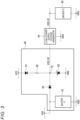
- FIG. 3 is a circuit diagram illustrating a configuration example of the recovery circuit 46.
- the recovery circuit 46 includes a buffer IC 43, a first diode 61, a resistor 62, a Zener diode 63, and a second diode 64.
- the channel group 41 is a member that ejects ink.
- the channel group 41 is configured by arranging a plurality of channels for ejecting ink according to an applied voltage.
- the channel group 41 includes a first piezoelectric member joined to the head substrate 47, a second piezoelectric member joined to the first piezoelectric member, a plurality of electrodes, and a nozzle plate.
- the first piezoelectric member and the second piezoelectric member are joined such that polarization directions thereof are opposite to each other.
- a plurality of parallel grooves extending from a side of the second piezoelectric member to the first piezoelectric member are formed in the first piezoelectric member and the second piezoelectric member.
- the electrode is formed in each groove.
- the first piezoelectric member and the second piezoelectric member sandwiched between two electrodes formed in two grooves are configured as actuators that are deformed by a potential difference between the two electrodes.
- the nozzle plate is the member that seals the grooves.
- a plurality of ejection nozzles for communicating the groove with the outside of the inkjet head 21 are formed in each groove.
- the groove sealed by the nozzle plate is filled with ink by the pump 19 and functions as a pressure chamber whose walls are configured with a pair of actuators.
- a drive waveform is input from the driver IC 45 to the electrode of the actuator that configures the wall of the pressure chamber, the actuator is deformed and the volume of the pressure chamber changes.
- pressure in the pressure chamber changes, and ink in the pressure chamber is ejected from the ejection nozzle.
- a combination of the pressure chamber and the ejection nozzle is referred to as a channel. That is, the channel group 41 is provided with channels corresponding to the number of grooves.
- the communication interface 42 is an interface for connecting the inkjet head 21 and the head controller 22.
- the communication interface 42 is provided with various terminals to which the transmission FPC 31 is connected.
- the communication interface 42 is provided with a plurality of power supply voltage input terminals to which the power supply voltage is supplied from the head controller 22 and a plurality of control signal input terminals to which the control signal is supplied from the head controller 22.
- the communication interface 42 is provided with four VAA input terminals respectively connected to a plurality of wirings for transmitting the power supply voltage VAA in the transmission FPC 31.
- the VAA input terminals are respectively connected to the power supply input terminals of the driver IC 45 for the power supply voltage VAA.
- the communication interface 42 is also provided with two VCC input terminals respectively connected to a plurality of wirings for transmitting the power supply voltage VCC in the transmission FPC 31.
- the VCC input terminals are respectively connected to power supply input terminals of the driver IC 45 for the power supply voltage VCC. At least one of the VCC input terminals is connected in parallel to an anode of the first diode 61 and the power supply input terminal of the driver IC 45 for the power supply voltage VCC.
- the power supply voltage VAA and the power supply voltage VCC are supplied from the head controller 22 to the recovery circuit 46 and the driver IC 45 via the transmission FPC 31 and the communication interface 42.
- the communication interface 42 is also provided with one VDD input terminal connected to the wiring for transmission of the power supply voltage VDD in the transmission FPC 31.
- the VDD input terminal is connected in parallel to an anode of the second diode 64 and a power supply input terminal of the buffer IC 43.
- a cathode of the second diode 64 is connected to a power supply input terminal of the logic power supply voltage generator 44 of the driver IC 45.
- the communication interface 42 is also provided with one CK input terminal connected to the wiring for transmission of the clock signal CK in the transmission FPC 31 and connected to the signal input terminal for the clock signal CK of the buffer IC 43.
- the communication interface 42 is also provided with one RST input terminal connected to the wiring for transmission of the reset signal RST in the transmission FPC 31 and connected to the signal input terminal for the reset signal RST of the buffer IC 43.
- the communication interface 42 is also provided with one INIT input terminal connected to the wiring for transmission of the initialization signal INIT in the transmission FPC 31 and connected to the signal input terminal for the initialization signal INIT of the buffer IC 43.
- the communication interface 42 is also provided with one SDI input terminal connected to the wiring for transmission of the print data SDI in the transmission FPC 31 and connected to the signal input terminal for the print data SDI of the buffer IC 43.
- the communication interface 42 is also provided with seven GND terminals that are grounded. With this configuration, the clock signal CK, the reset signal RST, the initialization signal INIT, and the print data SDI are supplied from the head controller 22 to the buffer IC 43 via the transmission FPC 31 and the communication interface 42.
- the buffer IC 43 is connected to the VDD input terminal of the communication interface 42 and operates with the power supply voltage VDD.
- the buffer IC 43 has an input-tolerant function.
- the buffer IC 43 changes (normalizes) a voltage level of the control signal supplied from the head controller 22 via the transmission FPC 31 and the communication interface 42, generates a control signal for controlling the driver IC 45, and supplies the control signal to the driver IC 45.
- the buffer IC 43 normalizes the clock signal CK input to the signal input terminal for the clock signal CK and converts the clock signal CK into a clock signal CK-IC.
- the buffer IC 43 normalizes the reset signal RST input to the signal input terminal for the reset signal RST and converts the reset signal RST into a reset signal RST-IC.
- the buffer IC 43 normalizes the initialization signal INIT input to the signal input terminal for the initialization signal INIT and converts the initialization signal INIT into an initialization signal INIT-IC.
- the buffer IC 43 normalizes the print data SDI input to the signal input terminal for the print data SDI and converts the print data SDI into print data SDI-IC.
- the buffer IC 43 inputs the clock signal CK-IC, the reset signal RST-IC, the initialization signal INIT-IC, and the print data SDI-IC to the driver IC 45.
- Each signal input terminal of the buffer IC 43 is configured as an input protection circuit. That is, the buffer IC 43 is an IC having a configuration with the input-tolerant function, in which each of the signal input terminal for the clock signal CK, the signal input terminal for the reset signal RST, the signal input terminal for the initialization signal INIT, and the signal input terminal for the print data SDI is not connected to a diode on a positive side (forward direction from signal input terminal to power supply input terminal). With this configuration, even if the voltage of the signal input to the signal input terminal becomes higher than the power supply voltage VDD, the current can be prevented from flowing from the signal input terminal to the power supply input terminal.
- the logic power supply voltage generator 44 (logic power supply circuit) converts the power supply voltage VDD into a power supply voltage VDD-IC according to the specifications of the driver IC 45.
- the logic power supply voltage generator 44 inputs the power supply voltage VDD-IC to the driver IC 45.
- the driver IC 45 is connected to the power supply voltage input terminals such as the VAA input terminal, the VCC input terminal, the VDD input terminal, and the like of the communication interface 42, the logic power supply voltage generator 44, the buffer IC 43, and the like.
- the driver IC 45 drives the channel group 41 based on the control signals output from the buffer IC 43.
- the driver IC 45 generates a drive waveform based on the control signals such as the clock signal CK-IC, the reset signal RST-IC, the initialization signal INIT-IC, and the print data SDI-IC input from the buffer IC 43 with the power supply voltage VAA, the power supply voltage VCC, the power supply voltage VDD-IC as the power supply input.
- the driver IC 45 inputs the drive waveform to the electrodes of the actuator of the channel group 41 via the electrode group 50 to deform the actuator and change the volume of the pressure chamber. With this configuration, the driver IC 45 causes ink in the pressure chamber to be ejected from the ejection nozzle.
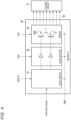
- FIG. 4 is a diagram illustrating a configuration example of the driver IC 45.
- the driver IC 45 includes a logic circuit 51, a level shifter 52, and a driver 53.
- the logic circuit 51 operates with the power supply voltage VDD-IC.
- the logic circuit 51 generates a drive signal for controlling the switching element of the driver 53 based on the signal CK-IC, the reset signal RST-IC, the initialization signal INIT-IC, and the print data SDI-IC input as the control signals.
- the logic circuit 51 inputs the drive signal to the level shifter 52.
- the logic circuit 51 includes a register that temporarily stores the print data SDI-IC.
- the terminals to which the control signals of the logic circuit 51 are input are also configured as the input protection circuit. That is, each of the signal input terminal for the clock signal CK-IC, the signal input terminal for the reset signal RST-IC, the signal input terminal for the initialization signal INIT-IC, and the signal input terminal for the print data SDI-IC is not connected to a diode on a positive side (forward direction from signal input terminal to power supply input terminal). With this configuration, even if the voltage of the signal input to the signal input terminal becomes higher than the power supply voltage VDD-IC, the current can be prevented from flowing from the signal input terminal to the power supply input terminal.
- the level shifter 52 converts a voltage level of the drive signal input from the logic circuit 51 using the power supply voltage VCC.
- the level shifter 52 inputs the drive signal whose voltage level is converted to the driver 53.
- the driver 53 is provided with two switching elements, each of which is configured with a p-MOSFET and an n-MOSFET, for each electrode of the channel group 41, for example.
- a gate of the switching element is connected to an output terminal of the level shifter 52.
- a source of the p-MOSFET is connected to the power supply voltage VAA, and a source of the n-MOSFET is connected to GND.
- the electrodes of the channel group 41 are connected to respective drains of two switching elements, which are connection points of the two switching elements.
- the driver 53 outputs the power supply voltage VAA or a GND level at timing in accordance with the drive signal input from the level shifter 52.
- the driver 53 inputs the drive waveform to each electrode of the channel group 41.
- the driver 53 causes ink to be ejected from the ejection nozzles of the channel group 41.
- the recovery circuit 46 reduces the voltage of the VCC input terminal of the communication interface 42 to supply the voltage to the power supply input terminal of the logic circuit 51 of the driver IC 45, and prevents the potential of the power supply input terminal of the logic circuit 51 of the driver IC 45 (or the power supply input terminal of the logic power supply voltage generator 44) from being supplied to the power supply input terminal of the buffer IC 43.
- the recovery circuit 46 supplies the power supply voltage VDD to the logic power supply voltage generator 44 as the power supply voltage VDD-DI (first voltage).
- the recovery circuit 46 includes the buffer IC 43, the first diode 61, the resistor 62, the Zener diode 63, and the second diode 64.
- the first diode 61 has an anode connected to the VCC input terminal as the power supply input terminal of the communication interface 42, and a cathode connected to the power supply input terminal of the logic power supply voltage generator 44 via the resistor 62.
- the first diode 61 is a Schottky diode.
- a connection point 70 is formed between the cathode of the first diode 61 and the power supply input terminal of the logic power supply voltage generator 44.
- the resistor 62 is formed between the cathode of the first diode 61 and the connection point 70.
- the resistor 62 reduces the power supply voltage VCC from the VCC input terminal and supplies the power supply voltage VCC to the logic power supply voltage generator 44.
- the resistance value of the resistor 62 is 10 K ⁇ .
- the second diode 64 has an anode connected to the VDD input terminal as the power supply voltage input terminal of the communication interface 42 and a cathode connected to the connection point 70.
- the second diode 64 is a Schottky diode.
- the Zener diode 63 also has an anode connected to the ground and a cathode connected to the connection point 70.
- the Zener diode 63 sets the upper limit of the voltage supplied to the logic power supply voltage generator 44.
- the Zener voltage of the Zener diode 63 is 4.8 V.
- the power supply voltage VDD-DI becomes 4.6 V if a connection failure does not occur in a path through which the power supply voltage VDD is transmitted.
- the logic power supply voltage generator 44 is supplied with the current primarily from the VDD input terminal, but is supplied with the current of 3.4 mA from the VCC input terminal.
- the power supply voltage VDD-DI is supplied from the VCC input terminal to the logic power supply voltage generator 44 via the first diode 61 and the resistor 62.
- the power supply voltage VDD-DI also becomes 4.6 V
- the logic power supply voltage generator 44 is supplied with the current of 3.4 mA from the VCC input terminal.
- the buffer IC 43 since the supply of power to the buffer IC 43 is stopped, the buffer IC 43 does not transmit the control signal to the driver IC 45. That is, the control signal is at a substantial GND level. Therefore, since the clock signal CK-IC is not supplied to the logic circuit 51 of the driver IC 45, the driver IC 45 does not consume power. Accordingly, even if the current from the logic power supply voltage generator 44 to the logic circuit 51 is reduced, the potential of the power supply voltage VDD-IC of the logic circuit 51 is maintained, and thus no problem arises.
- FIG. 5 is a timing chart illustrating the operation of the head controller 22 and the inkjet head 21 during normality.
- the horizontal axis indicates time and the vertical axis indicates voltage.
- FIG. 6 is a timing chart illustrating VCC (power supply voltage VCC), VDD (power supply voltage VDD), and VDD-DI (power supply voltage VDD-DI) in FIG. 5 .
- the horizontal axis indicates time and the vertical axis indicates voltage.
- the DC voltage DCV is supplied from the power supply circuit 23 to the head controller 22.
- the power supply voltage generator 32 If the DC voltage DCV is supplied, at timing t2, the power supply voltage generator 32 generates the power supply voltage VAA-IN, the power supply voltage VCC-IN, the power supply voltage VDD-IN, and the power supply voltage VDD-LOG.
- the power supply voltage generator 32 supplies the power supply voltage VAA-IN, the power supply voltage VCC-IN, and the power supply voltage VDD-IN to the power supply sequence circuit 33 and supplies the power supply voltage VDD-LOG to the control IC 35.
- the control IC 35 supplies the switching signal VOL-SW, which brings the power supply sequence circuit 33 into the enabled state, to the power supply sequence circuit 33. That is, the control IC 35 sets the switching signal VOL-SW to an H level. If the power supply sequence circuit 33 is brought into the enabled state by the switching signal VOL-SW, the power supply sequence circuit 33 starts outputting the power supply voltage VDD, the power supply voltage VCC, and the power supply voltage VAA in this order.
- the power supply sequence circuit 33 starts outputting the power supply voltage VDD.
- the recovery circuit 46 supplies the power supply voltage VDD to the logic power supply voltage generator 44 as the power supply voltage VDD-DI.
- the logic power supply voltage generator 44 of the inkjet head 21 supplies the power supply voltage VDD-IC to the driver IC 45.
- the control IC 35 starts outputting the clock signal CK and the initialization signal INIT to the buffer IC 43 of the inkjet head 21.
- the buffer IC 43 normalizes the clock signal CK and the initialization signal INIT, and supplies the clock signal CK-IC and the initialization signal INIT-IC to the driver IC 45.
- the control IC 35 starts outputting the reset signal RST to the buffer IC 43 of the inkjet head 21.
- the buffer IC 43 normalizes the reset signal RST and supplies the reset signal RST-IC to the driver IC 45.
- the power supply sequence circuit 33 starts outputting the power supply voltage VCC.
- the power supply voltage VCC is supplied to the driver IC 45.
- the power supply sequence circuit 33 starts outputting the power supply voltage VAA.
- the power supply voltage VAA is supplied to the driver IC 45.
- the control IC 35 starts outputting the print data SDI to the buffer IC 43 of the inkjet head 21.
- the buffer IC 43 normalizes the print data SDI and supplies the print data SDI-IC to the driver IC 45.
- the control IC 35 causes the inkjet head 21 to start printing.
- the control IC 35 lowers the initialization signal INIT from the H level to an L level by a predetermined number of clocks (for example, by one clock) at timing t9 if the output of the print data SDI for one line is completed.
- the initialization signal INIT-IC that the buffer IC 43 inputs to the driver IC 45 is also lowered to the L level.
- the logic circuit 51 of the driver IC 45 starts generating the drive signal using the clock signal CK-IC, the print data SDI-IC, and the power supply voltage VDD-IC with the fact that the initialization signal INIT-IC is lowered to the L level as a trigger.
- the level shifter 52 and the driver 53 start operating, and the drive waveform is input to the electrodes of the channel group 41. As a result, printing is executed.
- the control IC 35 recognizes that printing is completed, the control IC 35 supplies the switching signal VOL-SW, which brings the power supply sequence circuit 33 into the disabled state, to the power supply sequence circuit 33. That is, the control IC 35 sets the switching signal VOL-SW to the L level. If the power supply sequence circuit 33 is brought into the disabled state by the switching signal VOL-SW, the power supply sequence circuit 33 stops outputting the power supply voltage VAA, the power supply voltage VCC, and the power supply voltage VDD in this order.
- the power supply sequence circuit 33 stops outputting the power supply voltage VAA.
- the supply of the power supply voltage VAA to the driver IC 45 is stopped.
- the power supply sequence circuit 33 stops outputting the power supply voltage VCC.
- the supply of the power supply voltage VCC to the driver IC 45 is stopped.
- the power supply sequence circuit 33 stops outputting the power supply voltage VDD.
- the control IC 35 stops outputting the clock signal CK, the reset signal RST, and the initialization signal INIT. That is, at timing t13, the control IC 35 lowers the clock signal CK, the reset signal RST, and the initialization signal INIT from the H level to the L level.
- the clock signal CK-IC, the reset signal RST-IC, and the initialization signal INIT-IC supplied from the buffer IC 43 to the driver IC 45 are also lowered from the H level to the L level.
- the recovery circuit 46 stops outputting the power supply voltage VDD-DI. Thus, the power supply voltage is not supplied to the power supply input terminal of the logic power supply voltage generator 44 as well. As a result, the supply of the power supply voltage VDD-IC to the driver IC 45 is stopped.
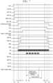
- FIG. 7 is a timing chart illustrating the operation of the head controller 22 and the inkjet head 21 during abnormality.
- the horizontal axis indicates time and the vertical axis indicates voltage.
- FIG. 8 is a timing chart illustrating VCC (power supply voltage VCC), VDD (power supply voltage VDD) and VDD-DI (power supply voltage VDD-DI) in FIG. 7 .
- the horizontal axis indicates time and the vertical axis indicates voltage.
- the DC voltage DCV is supplied from the power supply circuit 23 to the head controller 22.
- the power supply voltage generator 32 If the DC voltage DCV is supplied, at timing t2, the power supply voltage generator 32 generates the power supply voltage VAA-IN, the power supply voltage VCC-IN, the power supply voltage VDD-IN, and the power supply voltage VDD-LOG.
- the power supply voltage generator 32 supplies the power supply voltage VAA-IN, the power supply voltage VCC-IN, and the power supply voltage VDD-IN to the power supply sequence circuit 33 and supplies the power supply voltage VDD-LOG to the control IC 35.
- the control IC 35 supplies the switching signal VOL-SW, which brings the power supply sequence circuit 33 into the enabled state, to the power supply sequence circuit 33. That is, the control IC 35 sets the switching signal VOL-SW to the H level. If the power supply sequence circuit 33 is brought into the enabled state by the switching signal VOL-SW, the power supply sequence circuit 33 starts outputting the power supply voltage VDD, the power supply voltage VCC, and the power supply voltage VAA in this order.
- the power supply sequence circuit 33 starts outputting the power supply voltage VDD.
- the control IC 35 starts outputting the clock signal CK and the initialization signal INIT to the buffer IC 43 of the inkjet head 21. Since the power supply voltage VDD is not supplied, the buffer IC 43 continues to stop operating. Therefore, the clock signal CK-IC and the initialization signal INIT-IC are not supplied from the buffer IC 43 to the driver IC 45.
- the control IC 35 starts outputting the reset signal RST to the buffer IC 43 of the inkjet head 21. However, since the buffer IC 43 is not operating, the reset signal RST-IC is not supplied to the driver IC 45.
- the power supply sequence circuit 33 starts outputting the power supply voltage VCC.
- the power supply voltage VCC is supplied to the driver IC 45.
- the power supply voltage VCC is input to the power supply input terminal of the logic power supply voltage generator 44 via the first diode 61 and the resistor 62 as the power supply voltage VDD-DI.
- the upper limit of the power supply voltage VDD-DI is set by the Zener diode 63.
- the logic power supply voltage generator 44 generates the power supply voltage VDD-IC using the power supply voltage VDD-DI and starts supplying the power supply voltage VDD-IC to the driver IC 45.
- the power supply sequence circuit 33 starts outputting the power supply voltage VAA.
- the power supply voltage VAA is supplied to the driver IC 45.
- the control IC 35 starts outputting the print data SDI to the buffer IC 43 of the inkjet head 21.
- the buffer IC 43 is not operating, the print data SDI-IC is not supplied to the driver IC 45. In this case, printing is not executed.
- the control IC 35 causes the inkjet head 21 to start printing. For example, the control IC 35 lowers the initialization signal INIT from the H level to the L level by a predetermined number of clocks (for example, by one clock) at timing t9 if the output of the print data SDI for one line is completed. However, since the buffer IC 43 is not operating, printing is not executed.
- the control IC 35 supplies the switching signal VOL-SW, which brings the power supply sequence circuit 33 into the disabled state, to the power supply sequence circuit 33. That is, the control IC 35 sets the switching signal VOL-SW to the L level. If the power supply sequence circuit 33 is brought into the disabled state by the switching signal VOL-SW, the power supply sequence circuit 33 stops outputting the power supply voltage VAA, the power supply voltage VCC, and the power supply voltage VDD in this order.
- the power supply sequence circuit 33 stops outputting the power supply voltage VAA.
- the supply of the power supply voltage VAA to the driver IC 45 is stopped.
- the power supply sequence circuit 33 stops outputting the power supply voltage VCC.
- the supply of the power supply voltage VCC to the driver IC 45 is stopped.
- the recovery circuit 46 stops outputting the power supply voltage VDD-DI.
- the power supply voltage VDD-DI supplied to the power supply input terminal of the logic power supply voltage generator 44 is interrupted.
- the supply of the power supply voltage VDD-IC to the driver IC 45 is stopped.
- the power supply sequence circuit 33 stops outputting the power supply voltage VDD.
- the control IC 35 stops outputting the clock signal CK, the reset signal RST, and the initialization signal INIT. That is, at timing t13, the control IC 35 lowers the clock signal CK, the reset signal RST, and the initialization signal INIT from the H level to the L level.
- the drive signal is not supplied from the logic circuit 51 to the level shifter 52.
- the level shifter 52 is in an indefinite state if the power supply voltage VCC is supplied and the drive signal is not supplied from the logic circuit 51. In this case, the level shifter 52 may turn on the two switching elements of the driver 53 at the same time. If the two switching elements of the driver 53 are turned on at the same time, the power supply voltage VAA is applied to conductive paths of the two switching elements, and a through-current flows.
- the recovery circuit 46 can supply the power supply voltage VCC to the power supply input terminal of the logic power supply voltage generator 44 via the first diode 61 and the resistor 62.
- the logic power supply voltage generator 44 can generate the power supply voltage VDD-IC using the power supply voltage VCC. That is, the logic power supply voltage generator 44 can ensure the potential of the power supply input terminal to which the power supply voltage VDD-IC of the logic circuit 51 is input by the power supply voltage VCC.
- the recovery circuit 46 can prevent the through-current from flowing in the driver 53 even if the drive signal is not supplied from the logic circuit 51 to the level shifter 52 and the level shifter 52 is in the indefinite state. That is, the inkjet head 21 and the inkjet printer 1 according to this embodiment have high safety.
- the buffer IC 43 is in a state of not inputting the control signal to the driver IC 45 if the power supply voltage VDD is not supplied. That is, the buffer IC 43 is in a state of inputting the clock signal CK-IC, the reset signal RST-IC, the initialization signal INIT-IC, and the print data SDI-IC, all of which are at the substantial GND level, to the logic circuit 51 of the driver IC 45.
- the logic circuit 51 of the driver IC 45 since the logic circuit 51 of the driver IC 45 is not supplied with the clock signal CK-IC which is the reference clock, the logic circuit 51 does not operate and is in a state of not consuming power.
- the potential of the power supply input terminal of the logic circuit 51 can be ensured with the minimum current. As a result, the burden of power on the control IC 35 of the head controller 22 can be reduced.
- the second diode 64 which prevents the power supply voltage VDD-DI generated by the power supply voltage VCC from being inputted to the power supply input terminal of the buffer IC 43, is connected between the power supply input terminal of the buffer IC 43 and the connection point 70.
- the buffer IC 43 can be prevented from being operated if the connection failure exists in the path through which the power supply voltage VDD is transmitted. Further, if the connection failure exists in the path through which the power supply voltage VDD is transmitted, by preventing the buffer IC 43 and the driver IC 45 from being operated, the detection of defects by the control IC 35 of the head controller 22 can be facilitated.
Landscapes
- Engineering & Computer Science (AREA)
- Microelectronics & Electronic Packaging (AREA)
- Accessory Devices And Overall Control Thereof (AREA)
- Particle Formation And Scattering Control In Inkjet Printers (AREA)
Abstract
Description
- Embodiments described herein relate generally to an inkjet head and an inkjet printer.
- An inkjet printer that forms an image on a print medium in accordance with print data is put into practical use. The inkjet printer includes, for example, an inkjet head and a head controller that controls the inkjet head.
- The inkjet head includes an actuator for ejecting ink and a driver IC for driving the actuator under the control of the head controller.
- The head controller supplies a plurality of power supply voltages to the driver IC of the inkjet head. The head controller inputs and interrupts the plurality of power supply voltages based on a predetermined order. With this configuration, the head controller prevents a through-current from flowing in the driver IC.
- However, even if the head controller inputs and interrupts the plurality of power supply voltages in the predetermined order, if a connection failure exists in a wiring that connects the head controller and the driver IC, the order of inputting the power supply voltage supplied to the driver IC does not correspond to the predetermined order.
- In order to cope with such an event, a technique for supplying power by connecting a signal line for supplying a control signal to the driver IC is provided.
- In the related art, if the control signal is not in a high level state, the power supply voltage supplied to the driver IC may not be ensured.
- To this end, there is provided an inkjet head comprising: a driver IC that includes a logic circuit and a level shifter; a logic power supply circuit that inputs a first voltage to a power supply input terminal thereof and supplies a voltage to the logic circuit; and a first diode that is provided with an anode connected to a second voltage input to the level shifter and a cathode connected to the power supply input terminal of the logic power supply circuit.
- Preferred embodiments of the inkjet head are set out in dependent claims.
- There is also provided an inkjet printer comprising: an inkjet head that ejects ink onto a print medium; and a head controller that supplies a first voltage and a second voltage to the inkjet head, wherein the inkjet head includes a driver IC that includes a logic circuit and a level shifter, a logic power supply circuit that inputs the first voltage to a power supply input terminal thereof and supplies a voltage to the logic circuit, and a first diode that is provided with an anode connected to the second voltage input to the level shifter and a cathode connected to the power supply input terminal of the logic power supply circuit.
-
-
FIG. 1 is a block diagram illustrating a configuration example of an inkjet printer according to an embodiment; -
FIG. 2 is a circuit diagram conceptually illustrating a configuration example of an inkjet head and a head controller; -
FIG. 3 is a circuit diagram illustrating a configuration example of a recovery circuit; -
FIG. 4 is a diagram illustrating a configuration example of a driver IC; -
FIG. 5 is a timing chart illustrating an operation of the head controller and the inkjet head during normality; -
FIG. 6 is a timing chart illustrating the operation of the head controller and the inkjet head during normality; -
FIG. 7 is a timing chart illustrating an operation of the head controller and the inkjet head during abnormality; and -
FIG. 8 is a timing chart illustrating the operation of the head controller and the inkjet head during abnormality. - Embodiments provide an inkjet head and an inkjet printer having high safety.
- In general, according to one embodiment, there is provided an inkjet head including a driver IC, a logic power supply circuit, and a first diode. The driver IC includes a logic circuit and a level shifter. The logic power supply circuit inputs a first voltage to a power supply input terminal thereof and supplies a voltage to the logic circuit. The first diode is provided with an anode connected to a second voltage input to the level shifter and a cathode connected to the power supply input terminal of the logic power supply circuit.
- Hereinafter, embodiments will be described with reference to the drawings.
- An inkjet printer and an inkjet head according to an embodiment will be described below with reference to the drawings.
- First, an
inkjet printer 1 according to an embodiment will be described.FIG. 1 is a block diagram illustrating a configuration example of theinkjet printer 1 according to the embodiment. - The
inkjet printer 1 is an example of an inkjet recording apparatus. The inkjet recording apparatus is not limited to theinkjet printer 1, and may be another apparatus such as a copying machine. - The
inkjet printer 1, for example, performs various kinds of processing such as image formation while conveying a print medium, which is a recording medium. Theinkjet printer 1 includes a central processing unit (CPU) 11, a read only memory (ROM) 12, a random access memory (RAM) 13, acommunication interface 14, adisplay 15, anoperation unit 16, aconveyance motor 17, amotor drive circuit 18, apump 19, apump drive circuit 20, aninkjet head 21, ahead controller 22, and apower supply circuit 23. Furthermore, theinkjet printer 1 includes a paper feed cassette and a paper discharge tray (not illustrated). - The
CPU 11 is an operation element (for example, a processor) that executes operation processing. TheCPU 11 performs various kinds of processing based on data such as a program stored in theROM 12. TheCPU 11 functions as a control unit capable of executing various operations by executing the program stored in theROM 12. - The
ROM 12 is a read-only non-volatile memory. TheROM 12 stores a program, data used in the program, and the like. - The
RAM 13 is a volatile memory that functions as a working memory. TheRAM 13 temporarily stores data being processed by theCPU 11. TheRAM 13 also temporarily stores the program executed by theCPU 11. - The
communication interface 14 is an interface for communicating with other devices. Thecommunication interface 14 is used, for example, for communication with a host device that transmits a print command to theinkjet printer 1. Thecommunication interface 14 may perform wireless communication with other devices according to standards such as Bluetooth (registered trademark) or Wi-fi (registered trademark). - The
display 15 is a display device that displays a screen according to a video signal input from theCPU 11 or a display control unit such as a graphic controller (not illustrated). For example, thedisplay 15 displays a screen for setting theinkjet printer 1. - The
operation unit 16 generates an operation signal based on the operation. Theoperation unit 16 is, for example, a touch sensor, ten keys, a power key, a paper feed key, various function keys, or a keyboard. The touch sensor is, for example, a resistance film type touch sensor, or a capacitance type touch sensor. The touch sensor acquires information indicating a designated position within a certain area. The touch sensor is configured as a touch panel integrated with thedisplay 15 to generate a signal indicating a touched position on the screen displayed on thedisplay 15. - The
conveyance motor 17 rotates to operate conveyance members of a conveyance path (not illustrated) for conveying the print medium. The conveyance members are a belt, a roller, a guide, and the like for conveying the print medium. Theconveyance motor 17 conveys the print medium along the guide by driving the roller that operates in interlocking with the belt that holds the print medium. - The
motor drive circuit 18 is a circuit that drives theconveyance motor 17. Themotor drive circuit 18 conveys the print medium in the paper feed cassette to the paper discharge tray via theinkjet head 21 by driving theconveyance motor 17 according to a conveyance control signal input from theCPU 11. The paper feed cassette is a cassette that accommodates a plurality of print media. The paper discharge tray accommodates the print medium on which an image is formed by theinkjet printer 1 and discharged. - The
pump 19 includes, for example, a tube that communicates an ink tank (not illustrated) that stores ink with theinkjet head 21. Specifically, the tube communicates with a common ink chamber (not illustrated) of theinkjet head 21. - The
pump drive circuit 20 drives thepump 19 according to an ink supply control signal input from theCPU 11 to supply the ink in the ink tank to the common ink chamber of theinkjet head 21. - The
inkjet head 21 is an image forming unit that forms an image on the print medium. Theinkjet head 21 forms an image by ejecting ink onto the print medium conveyed by theconveyance motor 17 and a holding roller (not illustrated) based on a power supply voltage and a control signal supplied from thehead controller 22. Theinkjet printer 1 may include a plurality of inkjet heads 21 corresponding to respective colors such as cyan, magenta, yellow, and black. - The
head controller 22 is a circuit that controls theinkjet head 21. Thehead controller 22 causes ink to be ejected from theinkjet head 21 by operating theinkjet head 21. Thehead controller 22 supplies a plurality of power supply voltages to theinkjet head 21. Thehead controller 22 generates the control signal based on the print command input via thecommunication interface 14. Thehead controller 22 causes theinkjet head 21 to form an image on the print medium by supplying the power supply voltage and the control signal. - The
power supply circuit 23 converts AC power supplied from a commercial power source into DC power. Thepower supply circuit 23 supplies the DC power to each component in theinkjet printer 1. -
FIG. 2 is a circuit diagram illustrating a detailed configuration of theinkjet head 21 and thehead controller 22. Theinkjet head 21 and thehead controller 22 are connected to each other via a transmission flexible printed circuit (FPC) board (hereinafter referred to as a transmission FPC 31). With this configuration, thehead controller 22 can supply the power supply voltage and the control signal to theinkjet head 21. - First, the
head controller 22 will be described. - The
head controller 22 includes a powersupply voltage generator 32, a power supply sequence circuit 33, afirst communication interface 34, acontrol IC 35, and asecond communication interface 36. - The power
supply voltage generator 32 generates the plurality of power supply voltages necessary for the operation of theinkjet head 21 and a power supply voltage necessary for the operation of thecontrol IC 35 using a DC voltage DCV supplied from thepower supply circuit 23. The DC voltage DCV is, for example, 39 V. - For example, the power
supply voltage generator 32 generates a power supply voltage VAA-IN, a power supply voltage VCC-IN, a power supply voltage VDD-IN, and a power supply voltage VDD-LOG using the DC voltage DCV. The power supply voltage VAA-IN is a power supply voltage for generating a power supply voltage VAA used in theinkjet head 21. The power supply voltage VAA-IN is, for example, 20 V The power supply voltage VCC-IN is a power supply voltage for generating a power supply voltage VCC used in theinkjet head 21. The power supply voltage VCC-IN is, for example, 39 V. The power supply voltage VDD-IN is a power supply voltage for generating a power supply voltage VDD used in theinkjet head 21. The power supply voltage VDD-IN is, for example, 5 V The power supply voltage VDD-LOG is a power supply voltage for operating thecontrol IC 35. The power supply voltage VDD-LOG is, for example, 5 V. - The power
supply voltage generator 32 supplies the power supply voltage VAA-IN, the power supply voltage VCC-IN, and the power supply voltage VDD-IN to the power supply sequence circuit 33. The powersupply voltage generator 32 supplies the power supply voltage VDD-LOG to thecontrol IC 35. - The power supply sequence circuit 33 inputs and interrupts each power supply voltage to the
inkjet head 21. The power supply sequence circuit 33 inputs and interrupts each power supply voltage to theinkjet head 21 if the power supply sequence circuit 33 is in an enabled state. Further, if the power supply sequence circuit 33 is in a disabled state, the power supply sequence circuit 33 does not input and interrupt each power supply voltage. The power supply sequence circuit 33 switches between the enabled state and the disabled state under the control of thecontrol IC 35. - The power supply sequence circuit 33 outputs the power supply voltage VAA, the power supply voltage VCC (second voltage), and the power supply voltage VDD (first voltage) to the
inkjet head 21 based on the power supply voltage VAA-IN, the power supply voltage VCC-IN, and the power supply voltage VDD-IN supplied from the powersupply voltage generator 32. - The power supply sequence circuit 33 starts (input) the output of each power supply voltage based on a preset order (sequence). The power supply sequence circuit 33 stops (interrupts) the output of each power supply voltage based on a preset order (sequence). The power supply sequence circuit 33 inputs the power supply voltages in the order of the power supply voltage VDD, the power supply voltage VCC, and the power supply voltage VAA if the power is input. The power supply sequence circuit 33 interrupts the power supply voltages in the order of the power supply voltage VAA, the power supply voltage VCC, and the power supply voltage VDD if the power is interrupted.
- The
first communication interface 34 is an interface that connects theCPU 11 orcommunication interface 14 and thecontrol IC 35. The print command input to thefirst communication interface 34 from the host device connected via thecommunication interface 14 or from theCPU 11 is supplied to thecontrol IC 35. - The
control IC 35 operates with the power supply voltage VDD-LOG. Thecontrol IC 35 generates the control signal based on the print command input via thefirst communication interface 34. The control signal includes a clock signal CK, a reset signal RST, an initialization signal INIT, print data SDI, and the like. Thecontrol IC 35 outputs the control signals to theinkjet head 21 via thetransmission FPC 31. - The
control IC 35 also generates a switching signal VOL-SW for switching the operation of the power supply sequence circuit 33 between the enabled state and the disabled state. Thecontrol IC 35 switches the operation of the power supply sequence circuit 33 between the enabled state and the disabled state by inputting the switching signal VOL-SW to the power supply sequence circuit 33. For example, if thecontrol IC 35 is started up by being supplied with the power supply voltage VDD-LOG, thecontrol IC 35 switches the operation of the power supply sequence circuit 33 to the enabled state. Thecontrol IC 35 switches the operation of the power supply sequence circuit 33 to the disabled state if a predetermined signal is received from theCPU 11. - The
second communication interface 36 is an interface that connects theinkjet head 21 and thehead controller 22. Thesecond communication interface 36 is provided with various terminals to which thetransmission FPC 31 is connected. - For example, the
second communication interface 36 is provided with four terminals connected to an output terminal for the power supply voltage VAA of the power supply sequence circuit 33, two terminals connected to an output terminal for the power supply voltage VCC of the power supply sequence circuit 33, and one terminal connected to an output terminal for the power supply voltage VDD of the power supply sequence circuit 33. Thesecond communication interface 36 is also provided with one terminal connected to an output terminal for the clock signal CK of thecontrol IC 35, one terminal connected to an output terminal for the reset signal RST of thecontrol IC 35, one terminal connected to an output terminal for the initialization signal INIT of thecontrol IC 35, and one terminal connected to an output terminal for the print data SDI of thecontrol IC 35. In addition, thesecond communication interface 36 is provided with seven terminals that are grounded. Thetransmission FPC 31 is also provided with a plurality of wirings connected to respective terminals of thesecond communication interface 36. - The power supply voltage VAA, the power supply voltage VCC, and the power supply voltage VDD output from the power supply sequence circuit 33, and the clock signal CK, the reset signal RST, the initialization signal INIT, and the print data SDI output from the
control IC 35 are supplied to theinkjet head 21 connected via thesecond communication interface 36 and thetransmission FPC 31. - The number of terminals provided in the
second communication interface 36 and the number of wirings (number of cores) in thetransmission FPC 31 can be determined based on the current consumption in theinkjet head 21, and are not limited to the numbers described above. That is, the number of terminals and wirings may be changed as appropriate according to the specifications of theinkjet head 21 and thehead controller 22. - Next, the
inkjet head 21 will be described. - The
inkjet head 21 includes achannel group 41, acommunication interface 42, a logic powersupply voltage generator 44, adriver IC 45, arecovery circuit 46, ahead substrate 47, and anelectrode group 50. Thechannel group 41, thecommunication interface 42, the logic powersupply voltage generator 44, thedriver IC 45, therecovery circuit 46, and theelectrode group 50 are mounted on thehead substrate 47. -
FIG. 3 is a circuit diagram illustrating a configuration example of therecovery circuit 46. As illustrated inFIG. 3 , therecovery circuit 46 includes abuffer IC 43, afirst diode 61, aresistor 62, aZener diode 63, and asecond diode 64. - The
channel group 41 is a member that ejects ink. Thechannel group 41 is configured by arranging a plurality of channels for ejecting ink according to an applied voltage. Thechannel group 41 includes a first piezoelectric member joined to thehead substrate 47, a second piezoelectric member joined to the first piezoelectric member, a plurality of electrodes, and a nozzle plate. - The first piezoelectric member and the second piezoelectric member are joined such that polarization directions thereof are opposite to each other. A plurality of parallel grooves extending from a side of the second piezoelectric member to the first piezoelectric member are formed in the first piezoelectric member and the second piezoelectric member. The electrode is formed in each groove. The first piezoelectric member and the second piezoelectric member sandwiched between two electrodes formed in two grooves are configured as actuators that are deformed by a potential difference between the two electrodes.
- The nozzle plate is the member that seals the grooves. In the nozzle plate, a plurality of ejection nozzles for communicating the groove with the outside of the
inkjet head 21 are formed in each groove. The groove sealed by the nozzle plate is filled with ink by thepump 19 and functions as a pressure chamber whose walls are configured with a pair of actuators. - If a drive waveform is input from the
driver IC 45 to the electrode of the actuator that configures the wall of the pressure chamber, the actuator is deformed and the volume of the pressure chamber changes. With this configuration, pressure in the pressure chamber changes, and ink in the pressure chamber is ejected from the ejection nozzle. In this example, a combination of the pressure chamber and the ejection nozzle is referred to as a channel. That is, thechannel group 41 is provided with channels corresponding to the number of grooves. - The
communication interface 42 is an interface for connecting theinkjet head 21 and thehead controller 22. Thecommunication interface 42 is provided with various terminals to which thetransmission FPC 31 is connected. - The
communication interface 42 is provided with a plurality of power supply voltage input terminals to which the power supply voltage is supplied from thehead controller 22 and a plurality of control signal input terminals to which the control signal is supplied from thehead controller 22. For example, thecommunication interface 42 is provided with four VAA input terminals respectively connected to a plurality of wirings for transmitting the power supply voltage VAA in thetransmission FPC 31. The VAA input terminals are respectively connected to the power supply input terminals of thedriver IC 45 for the power supply voltage VAA. Thecommunication interface 42 is also provided with two VCC input terminals respectively connected to a plurality of wirings for transmitting the power supply voltage VCC in thetransmission FPC 31. The VCC input terminals are respectively connected to power supply input terminals of thedriver IC 45 for the power supply voltage VCC. At least one of the VCC input terminals is connected in parallel to an anode of thefirst diode 61 and the power supply input terminal of thedriver IC 45 for the power supply voltage VCC. With this configuration, the power supply voltage VAA and the power supply voltage VCC are supplied from thehead controller 22 to therecovery circuit 46 and thedriver IC 45 via thetransmission FPC 31 and thecommunication interface 42. - The
communication interface 42 is also provided with one VDD input terminal connected to the wiring for transmission of the power supply voltage VDD in thetransmission FPC 31. The VDD input terminal is connected in parallel to an anode of thesecond diode 64 and a power supply input terminal of thebuffer IC 43. A cathode of thesecond diode 64 is connected to a power supply input terminal of the logic powersupply voltage generator 44 of thedriver IC 45. With this configuration, the power supply voltage VDD is supplied from thehead controller 22 to the logic powersupply voltage generator 44 and thebuffer IC 43 via thetransmission FPC 31 and thecommunication interface 42. - The
communication interface 42 is also provided with one CK input terminal connected to the wiring for transmission of the clock signal CK in thetransmission FPC 31 and connected to the signal input terminal for the clock signal CK of thebuffer IC 43. Thecommunication interface 42 is also provided with one RST input terminal connected to the wiring for transmission of the reset signal RST in thetransmission FPC 31 and connected to the signal input terminal for the reset signal RST of thebuffer IC 43. Thecommunication interface 42 is also provided with one INIT input terminal connected to the wiring for transmission of the initialization signal INIT in thetransmission FPC 31 and connected to the signal input terminal for the initialization signal INIT of thebuffer IC 43. Thecommunication interface 42 is also provided with one SDI input terminal connected to the wiring for transmission of the print data SDI in thetransmission FPC 31 and connected to the signal input terminal for the print data SDI of thebuffer IC 43. Thecommunication interface 42 is also provided with seven GND terminals that are grounded. With this configuration, the clock signal CK, the reset signal RST, the initialization signal INIT, and the print data SDI are supplied from thehead controller 22 to thebuffer IC 43 via thetransmission FPC 31 and thecommunication interface 42. - The
buffer IC 43 is connected to the VDD input terminal of thecommunication interface 42 and operates with the power supply voltage VDD. Thebuffer IC 43 has an input-tolerant function. Thebuffer IC 43 changes (normalizes) a voltage level of the control signal supplied from thehead controller 22 via thetransmission FPC 31 and thecommunication interface 42, generates a control signal for controlling thedriver IC 45, and supplies the control signal to thedriver IC 45. For example, thebuffer IC 43 normalizes the clock signal CK input to the signal input terminal for the clock signal CK and converts the clock signal CK into a clock signal CK-IC. Thebuffer IC 43 normalizes the reset signal RST input to the signal input terminal for the reset signal RST and converts the reset signal RST into a reset signal RST-IC. Thebuffer IC 43 normalizes the initialization signal INIT input to the signal input terminal for the initialization signal INIT and converts the initialization signal INIT into an initialization signal INIT-IC. Thebuffer IC 43 normalizes the print data SDI input to the signal input terminal for the print data SDI and converts the print data SDI into print data SDI-IC. Thebuffer IC 43 inputs the clock signal CK-IC, the reset signal RST-IC, the initialization signal INIT-IC, and the print data SDI-IC to thedriver IC 45. - Each signal input terminal of the
buffer IC 43 is configured as an input protection circuit. That is, thebuffer IC 43 is an IC having a configuration with the input-tolerant function, in which each of the signal input terminal for the clock signal CK, the signal input terminal for the reset signal RST, the signal input terminal for the initialization signal INIT, and the signal input terminal for the print data SDI is not connected to a diode on a positive side (forward direction from signal input terminal to power supply input terminal). With this configuration, even if the voltage of the signal input to the signal input terminal becomes higher than the power supply voltage VDD, the current can be prevented from flowing from the signal input terminal to the power supply input terminal. - The logic power supply voltage generator 44 (logic power supply circuit) converts the power supply voltage VDD into a power supply voltage VDD-IC according to the specifications of the
driver IC 45. The logic powersupply voltage generator 44 inputs the power supply voltage VDD-IC to thedriver IC 45. - The
driver IC 45 is connected to the power supply voltage input terminals such as the VAA input terminal, the VCC input terminal, the VDD input terminal, and the like of thecommunication interface 42, the logic powersupply voltage generator 44, thebuffer IC 43, and the like. Thedriver IC 45 drives thechannel group 41 based on the control signals output from thebuffer IC 43. - The
driver IC 45 generates a drive waveform based on the control signals such as the clock signal CK-IC, the reset signal RST-IC, the initialization signal INIT-IC, and the print data SDI-IC input from thebuffer IC 43 with the power supply voltage VAA, the power supply voltage VCC, the power supply voltage VDD-IC as the power supply input. Thedriver IC 45 inputs the drive waveform to the electrodes of the actuator of thechannel group 41 via theelectrode group 50 to deform the actuator and change the volume of the pressure chamber. With this configuration, thedriver IC 45 causes ink in the pressure chamber to be ejected from the ejection nozzle. -
FIG. 4 is a diagram illustrating a configuration example of thedriver IC 45. Thedriver IC 45 includes alogic circuit 51, alevel shifter 52, and adriver 53. - The
logic circuit 51 operates with the power supply voltage VDD-IC. Thelogic circuit 51 generates a drive signal for controlling the switching element of thedriver 53 based on the signal CK-IC, the reset signal RST-IC, the initialization signal INIT-IC, and the print data SDI-IC input as the control signals. Thelogic circuit 51 inputs the drive signal to thelevel shifter 52. Thelogic circuit 51 includes a register that temporarily stores the print data SDI-IC. - The terminals to which the control signals of the
logic circuit 51 are input are also configured as the input protection circuit. That is, each of the signal input terminal for the clock signal CK-IC, the signal input terminal for the reset signal RST-IC, the signal input terminal for the initialization signal INIT-IC, and the signal input terminal for the print data SDI-IC is not connected to a diode on a positive side (forward direction from signal input terminal to power supply input terminal). With this configuration, even if the voltage of the signal input to the signal input terminal becomes higher than the power supply voltage VDD-IC, the current can be prevented from flowing from the signal input terminal to the power supply input terminal. - The
level shifter 52 converts a voltage level of the drive signal input from thelogic circuit 51 using the power supply voltage VCC. Thelevel shifter 52 inputs the drive signal whose voltage level is converted to thedriver 53. - The
driver 53 is provided with two switching elements, each of which is configured with a p-MOSFET and an n-MOSFET, for each electrode of thechannel group 41, for example. A gate of the switching element is connected to an output terminal of thelevel shifter 52. A source of the p-MOSFET is connected to the power supply voltage VAA, and a source of the n-MOSFET is connected to GND. The electrodes of thechannel group 41 are connected to respective drains of two switching elements, which are connection points of the two switching elements. With such a configuration, thedriver 53 outputs the power supply voltage VAA or a GND level at timing in accordance with the drive signal input from thelevel shifter 52. Thus, thedriver 53 inputs the drive waveform to each electrode of thechannel group 41. As a result, thedriver 53 causes ink to be ejected from the ejection nozzles of thechannel group 41. - The
recovery circuit 46 reduces the voltage of the VCC input terminal of thecommunication interface 42 to supply the voltage to the power supply input terminal of thelogic circuit 51 of thedriver IC 45, and prevents the potential of the power supply input terminal of thelogic circuit 51 of the driver IC 45 (or the power supply input terminal of the logic power supply voltage generator 44) from being supplied to the power supply input terminal of thebuffer IC 43. Therecovery circuit 46 supplies the power supply voltage VDD to the logic powersupply voltage generator 44 as the power supply voltage VDD-DI (first voltage). - As described above, the
recovery circuit 46 includes thebuffer IC 43, thefirst diode 61, theresistor 62, theZener diode 63, and thesecond diode 64. - The
first diode 61 has an anode connected to the VCC input terminal as the power supply input terminal of thecommunication interface 42, and a cathode connected to the power supply input terminal of the logic powersupply voltage generator 44 via theresistor 62. Thefirst diode 61 is a Schottky diode. - A
connection point 70 is formed between the cathode of thefirst diode 61 and the power supply input terminal of the logic powersupply voltage generator 44. Theresistor 62 is formed between the cathode of thefirst diode 61 and theconnection point 70. - The
resistor 62 reduces the power supply voltage VCC from the VCC input terminal and supplies the power supply voltage VCC to the logic powersupply voltage generator 44. For example, the resistance value of theresistor 62 is 10 KΩ. - As described above, the
second diode 64 has an anode connected to the VDD input terminal as the power supply voltage input terminal of thecommunication interface 42 and a cathode connected to theconnection point 70. Thesecond diode 64 is a Schottky diode. - The
Zener diode 63 also has an anode connected to the ground and a cathode connected to theconnection point 70. TheZener diode 63 sets the upper limit of the voltage supplied to the logic powersupply voltage generator 44. For example, the Zener voltage of theZener diode 63 is 4.8 V. - In the configuration described above, the power supply voltage VDD-DI becomes 4.6 V if a connection failure does not occur in a path through which the power supply voltage VDD is transmitted. The logic power
supply voltage generator 44 is supplied with the current primarily from the VDD input terminal, but is supplied with the current of 3.4 mA from the VCC input terminal. - If the connection failure occurs in the path through which the power supply voltage VDD is transmitted, the power supply voltage VDD-DI is supplied from the VCC input terminal to the logic power
supply voltage generator 44 via thefirst diode 61 and theresistor 62. The power supply voltage VDD-DI also becomes 4.6 V The logic powersupply voltage generator 44 is supplied with the current of 3.4 mA from the VCC input terminal. - In this case, since the supply of power to the
buffer IC 43 is stopped, thebuffer IC 43 does not transmit the control signal to thedriver IC 45. That is, the control signal is at a substantial GND level. Therefore, since the clock signal CK-IC is not supplied to thelogic circuit 51 of thedriver IC 45, thedriver IC 45 does not consume power. Accordingly, even if the current from the logic powersupply voltage generator 44 to thelogic circuit 51 is reduced, the potential of the power supply voltage VDD-IC of thelogic circuit 51 is maintained, and thus no problem arises. - Next, the operation if the connection failure does not exist in the path through which the power supply voltage VDD is transmitted (during normality) will be described.
-
FIG. 5 is a timing chart illustrating the operation of thehead controller 22 and theinkjet head 21 during normality. InFIG. 5 , the horizontal axis indicates time and the vertical axis indicates voltage.FIG. 6 is a timing chart illustrating VCC (power supply voltage VCC), VDD (power supply voltage VDD), and VDD-DI (power supply voltage VDD-DI) inFIG. 5 . InFIG. 6 , the horizontal axis indicates time and the vertical axis indicates voltage. - At timing t1, if the
inkjet printer 1 is powered on, the DC voltage DCV is supplied from thepower supply circuit 23 to thehead controller 22. - If the DC voltage DCV is supplied, at timing t2, the power
supply voltage generator 32 generates the power supply voltage VAA-IN, the power supply voltage VCC-IN, the power supply voltage VDD-IN, and the power supply voltage VDD-LOG. The powersupply voltage generator 32 supplies the power supply voltage VAA-IN, the power supply voltage VCC-IN, and the power supply voltage VDD-IN to the power supply sequence circuit 33 and supplies the power supply voltage VDD-LOG to thecontrol IC 35. - At timing t3, if the print command is input to the
control IC 35, thecontrol IC 35 supplies the switching signal VOL-SW, which brings the power supply sequence circuit 33 into the enabled state, to the power supply sequence circuit 33. That is, thecontrol IC 35 sets the switching signal VOL-SW to an H level. If the power supply sequence circuit 33 is brought into the enabled state by the switching signal VOL-SW, the power supply sequence circuit 33 starts outputting the power supply voltage VDD, the power supply voltage VCC, and the power supply voltage VAA in this order. - At timing t4, the power supply sequence circuit 33 starts outputting the power supply voltage VDD. At this time, the
recovery circuit 46 supplies the power supply voltage VDD to the logic powersupply voltage generator 44 as the power supply voltage VDD-DI. At timing t4, the logic powersupply voltage generator 44 of theinkjet head 21 supplies the power supply voltage VDD-IC to thedriver IC 45. At timing t4, thecontrol IC 35 starts outputting the clock signal CK and the initialization signal INIT to thebuffer IC 43 of theinkjet head 21. At timing t4, thebuffer IC 43 normalizes the clock signal CK and the initialization signal INIT, and supplies the clock signal CK-IC and the initialization signal INIT-IC to thedriver IC 45. - At timing t5, the
control IC 35 starts outputting the reset signal RST to thebuffer IC 43 of theinkjet head 21. At timing t5, thebuffer IC 43 normalizes the reset signal RST and supplies the reset signal RST-IC to thedriver IC 45. - At timing t6, the power supply sequence circuit 33 starts outputting the power supply voltage VCC. Thus, the power supply voltage VCC is supplied to the
driver IC 45. - At timing t7, the power supply sequence circuit 33 starts outputting the power supply voltage VAA. Thus, the power supply voltage VAA is supplied to the
driver IC 45. - At timing t8, the
control IC 35 starts outputting the print data SDI to thebuffer IC 43 of theinkjet head 21. At timing t8, thebuffer IC 43 normalizes the print data SDI and supplies the print data SDI-IC to thedriver IC 45. - At timing t9, the
control IC 35 causes theinkjet head 21 to start printing. For example, thecontrol IC 35 lowers the initialization signal INIT from the H level to an L level by a predetermined number of clocks (for example, by one clock) at timing t9 if the output of the print data SDI for one line is completed. Thus, the initialization signal INIT-IC that thebuffer IC 43 inputs to thedriver IC 45 is also lowered to the L level. Thelogic circuit 51 of thedriver IC 45 starts generating the drive signal using the clock signal CK-IC, the print data SDI-IC, and the power supply voltage VDD-IC with the fact that the initialization signal INIT-IC is lowered to the L level as a trigger. Thus, thelevel shifter 52 and thedriver 53 start operating, and the drive waveform is input to the electrodes of thechannel group 41. As a result, printing is executed. - At timing t10, if the
control IC 35 recognizes that printing is completed, thecontrol IC 35 supplies the switching signal VOL-SW, which brings the power supply sequence circuit 33 into the disabled state, to the power supply sequence circuit 33. That is, thecontrol IC 35 sets the switching signal VOL-SW to the L level. If the power supply sequence circuit 33 is brought into the disabled state by the switching signal VOL-SW, the power supply sequence circuit 33 stops outputting the power supply voltage VAA, the power supply voltage VCC, and the power supply voltage VDD in this order. - At timing 111, the power supply sequence circuit 33 stops outputting the power supply voltage VAA. Thus, the supply of the power supply voltage VAA to the
driver IC 45 is stopped. - At timing t12, the power supply sequence circuit 33 stops outputting the power supply voltage VCC. Thus, the supply of the power supply voltage VCC to the
driver IC 45 is stopped. - At timing t13, the power supply sequence circuit 33 stops outputting the power supply voltage VDD. At timing t13, the
control IC 35 stops outputting the clock signal CK, the reset signal RST, and the initialization signal INIT. That is, at timing t13, thecontrol IC 35 lowers the clock signal CK, the reset signal RST, and the initialization signal INIT from the H level to the L level. Thus, the clock signal CK-IC, the reset signal RST-IC, and the initialization signal INIT-IC supplied from thebuffer IC 43 to thedriver IC 45 are also lowered from the H level to the L level. Therecovery circuit 46 stops outputting the power supply voltage VDD-DI. Thus, the power supply voltage is not supplied to the power supply input terminal of the logic powersupply voltage generator 44 as well. As a result, the supply of the power supply voltage VDD-IC to thedriver IC 45 is stopped. - Next, the operation if the connection failure exists in the path through which the power supply voltage VDD is transmitted (during abnormality) will be described.
-
FIG. 7 is a timing chart illustrating the operation of thehead controller 22 and theinkjet head 21 during abnormality. InFIG. 7 , the horizontal axis indicates time and the vertical axis indicates voltage.FIG. 8 is a timing chart illustrating VCC (power supply voltage VCC), VDD (power supply voltage VDD) and VDD-DI (power supply voltage VDD-DI) inFIG. 7 . InFIG. 8 , the horizontal axis indicates time and the vertical axis indicates voltage. - At timing t1, if the
inkjet printer 1 is powered on, the DC voltage DCV is supplied from thepower supply circuit 23 to thehead controller 22. - If the DC voltage DCV is supplied, at timing t2, the power
supply voltage generator 32 generates the power supply voltage VAA-IN, the power supply voltage VCC-IN, the power supply voltage VDD-IN, and the power supply voltage VDD-LOG. The powersupply voltage generator 32 supplies the power supply voltage VAA-IN, the power supply voltage VCC-IN, and the power supply voltage VDD-IN to the power supply sequence circuit 33 and supplies the power supply voltage VDD-LOG to thecontrol IC 35. - At timing t3, if the print command is input to the
control IC 35, thecontrol IC 35 supplies the switching signal VOL-SW, which brings the power supply sequence circuit 33 into the enabled state, to the power supply sequence circuit 33. That is, thecontrol IC 35 sets the switching signal VOL-SW to the H level. If the power supply sequence circuit 33 is brought into the enabled state by the switching signal VOL-SW, the power supply sequence circuit 33 starts outputting the power supply voltage VDD, the power supply voltage VCC, and the power supply voltage VAA in this order. - At timing t4, the power supply sequence circuit 33 starts outputting the power supply voltage VDD. However, when the connection failure exists in the path through which the power supply voltage VDD is transmitted, the power supply voltage VDD is not supplied to the logic power
supply voltage generator 44 and thebuffer IC 43 of theinkjet head 21. At timing t4, thecontrol IC 35 starts outputting the clock signal CK and the initialization signal INIT to thebuffer IC 43 of theinkjet head 21. Since the power supply voltage VDD is not supplied, thebuffer IC 43 continues to stop operating. Therefore, the clock signal CK-IC and the initialization signal INIT-IC are not supplied from thebuffer IC 43 to thedriver IC 45. - At timing t5, the
control IC 35 starts outputting the reset signal RST to thebuffer IC 43 of theinkjet head 21. However, since thebuffer IC 43 is not operating, the reset signal RST-IC is not supplied to thedriver IC 45. - At timing t6, the power supply sequence circuit 33 starts outputting the power supply voltage VCC. Thus, the power supply voltage VCC is supplied to the
driver IC 45. The power supply voltage VCC is input to the power supply input terminal of the logic powersupply voltage generator 44 via thefirst diode 61 and theresistor 62 as the power supply voltage VDD-DI. The upper limit of the power supply voltage VDD-DI is set by theZener diode 63. The logic powersupply voltage generator 44 generates the power supply voltage VDD-IC using the power supply voltage VDD-DI and starts supplying the power supply voltage VDD-IC to thedriver IC 45. - At timing t7, the power supply sequence circuit 33 starts outputting the power supply voltage VAA. Thus, the power supply voltage VAA is supplied to the
driver IC 45. - At timing t8, the
control IC 35 starts outputting the print data SDI to thebuffer IC 43 of theinkjet head 21. However, since thebuffer IC 43 is not operating, the print data SDI-IC is not supplied to thedriver IC 45. In this case, printing is not executed. - At timing t9, the
control IC 35 causes theinkjet head 21 to start printing. For example, thecontrol IC 35 lowers the initialization signal INIT from the H level to the L level by a predetermined number of clocks (for example, by one clock) at timing t9 if the output of the print data SDI for one line is completed. However, since thebuffer IC 43 is not operating, printing is not executed. - At timing t10, the
control IC 35 supplies the switching signal VOL-SW, which brings the power supply sequence circuit 33 into the disabled state, to the power supply sequence circuit 33. That is, thecontrol IC 35 sets the switching signal VOL-SW to the L level. If the power supply sequence circuit 33 is brought into the disabled state by the switching signal VOL-SW, the power supply sequence circuit 33 stops outputting the power supply voltage VAA, the power supply voltage VCC, and the power supply voltage VDD in this order. - At timing 111, the power supply sequence circuit 33 stops outputting the power supply voltage VAA. Thus, the supply of the power supply voltage VAA to the
driver IC 45 is stopped. - At timing t12, the power supply sequence circuit 33 stops outputting the power supply voltage VCC. Thus, the supply of the power supply voltage VCC to the
driver IC 45 is stopped. Therecovery circuit 46 stops outputting the power supply voltage VDD-DI. Thus, the power supply voltage VDD-DI supplied to the power supply input terminal of the logic powersupply voltage generator 44 is interrupted. As a result, the supply of the power supply voltage VDD-IC to thedriver IC 45 is stopped. - At timing t13, the power supply sequence circuit 33 stops outputting the power supply voltage VDD. At timing t13, the
control IC 35 stops outputting the clock signal CK, the reset signal RST, and the initialization signal INIT. That is, at timing t13, thecontrol IC 35 lowers the clock signal CK, the reset signal RST, and the initialization signal INIT from the H level to the L level. - For example, if the power supply voltage VAA and the power supply voltage VCC are supplied to the
driver IC 45 and the power supply voltage VDD-IC is not supplied to thedriver IC 45, the drive signal is not supplied from thelogic circuit 51 to thelevel shifter 52. Thelevel shifter 52 is in an indefinite state if the power supply voltage VCC is supplied and the drive signal is not supplied from thelogic circuit 51. In this case, thelevel shifter 52 may turn on the two switching elements of thedriver 53 at the same time. If the two switching elements of thedriver 53 are turned on at the same time, the power supply voltage VAA is applied to conductive paths of the two switching elements, and a through-current flows. - However, as described above, even if the connection failure exists in the path through which the power supply voltage VDD is transmitted, and the power supply voltage VDD is not supplied to the
buffer IC 43 and the logic powersupply voltage generator 44, therecovery circuit 46 can supply the power supply voltage VCC to the power supply input terminal of the logic powersupply voltage generator 44 via thefirst diode 61 and theresistor 62. With this configuration, the logic powersupply voltage generator 44 can generate the power supply voltage VDD-IC using the power supply voltage VCC. That is, the logic powersupply voltage generator 44 can ensure the potential of the power supply input terminal to which the power supply voltage VDD-IC of thelogic circuit 51 is input by the power supply voltage VCC. As a result, therecovery circuit 46 can prevent the through-current from flowing in thedriver 53 even if the drive signal is not supplied from thelogic circuit 51 to thelevel shifter 52 and thelevel shifter 52 is in the indefinite state. That is, theinkjet head 21 and theinkjet printer 1 according to this embodiment have high safety. - In addition, the
buffer IC 43 is in a state of not inputting the control signal to thedriver IC 45 if the power supply voltage VDD is not supplied. That is, thebuffer IC 43 is in a state of inputting the clock signal CK-IC, the reset signal RST-IC, the initialization signal INIT-IC, and the print data SDI-IC, all of which are at the substantial GND level, to thelogic circuit 51 of thedriver IC 45. In this case, since thelogic circuit 51 of thedriver IC 45 is not supplied with the clock signal CK-IC which is the reference clock, thelogic circuit 51 does not operate and is in a state of not consuming power. Thus, the potential of the power supply input terminal of thelogic circuit 51 can be ensured with the minimum current. As a result, the burden of power on thecontrol IC 35 of thehead controller 22 can be reduced. - The
second diode 64, which prevents the power supply voltage VDD-DI generated by the power supply voltage VCC from being inputted to the power supply input terminal of thebuffer IC 43, is connected between the power supply input terminal of thebuffer IC 43 and theconnection point 70. With this configuration, thebuffer IC 43 can be prevented from being operated if the connection failure exists in the path through which the power supply voltage VDD is transmitted. Further, if the connection failure exists in the path through which the power supply voltage VDD is transmitted, by preventing thebuffer IC 43 and thedriver IC 45 from being operated, the detection of defects by thecontrol IC 35 of thehead controller 22 can be facilitated. - While certain embodiments have been described, these embodiments have been presented by way of example only, and are not intended to limit the scope of the inventions. Indeed, the novel embodiments described herein may be embodied in a variety of other forms; furthermore, various omissions, substitutions and changes in the form of the embodiments described herein may be made without departing from the inventions. The accompanying claims are intended to cover such forms or modifications as would fall within the scope of the inventions.
Claims (9)
- An inkjet head (21) comprising:a driver IC (45) that includes a logic circuit and a level shifter;a logic power supply circuit that inputs a first voltage to a power supply input terminal thereof and supplies a voltage to the logic circuit; anda first diode (61) that is provided with an anode connected to a second voltage input to the level shifter and a cathode connected to the power supply input terminal of the logic power supply circuit.
- The head according to claim 1, wherein the first diode is a Schottky diode.
- The head according to claim 1 or 2, further comprising:a buffer IC (43) that inputs the first voltage to a power supply input terminal thereof and supplies a control signal to the logic circuit; anda second diode (64) that is provided with an anode connected to the power supply input terminal of the buffer IC and a cathode connected to a connection point between the cathode of the first diode and the power supply input terminal of the logic power supply circuit.
- The head according to claim 3, further comprising:
a Zener diode that is provided with an anode connected to GND and a cathode connected to the connection point. - The head according to claim 3 or 4, further comprising:
a resistor that is formed between the cathode of the first diode and the connection point. - The head according to any one of claims 3 to 5, wherein
the buffer IC is provided with an input-tolerant function. - The head according to any one of claims 3 to 6, wherein
each signal input terminal of the buffer IC is configured as an input protection circuit. - The head according to any one of claims 3 to 7, whereinthe driver IC further includes a driver,the logic circuit generates a drive signal, andthe level shifter converts a voltage level of the drive signal input from the logic circuit and inputs the converted drive signal to the driver.
- An inkjet printer comprising:an inkjet head (21) that ejects ink onto a print medium; anda head controller that supplies a first voltage and a second voltage to the inkjet head, whereinthe inkjet head includesa driver IC (45) that includes a logic circuit and a level shifter,a logic power supply circuit that inputs the first voltage to a power supply input terminal thereof and supplies a voltage to the logic circuit, anda first diode (61) that is provided with an anode connected to the second voltage input to the level shifter and a cathode connected to the power supply input terminal of the logic power supply circuit.
Applications Claiming Priority (1)
| Application Number | Priority Date | Filing Date | Title |
|---|---|---|---|
| JP2023006653A JP2024102635A (en) | 2023-01-19 | 2023-01-19 | Inkjet head and inkjet printer |
Publications (1)
| Publication Number | Publication Date |
|---|---|
| EP4403364A1 true EP4403364A1 (en) | 2024-07-24 |
Family
ID=88511396
Family Applications (1)
| Application Number | Title | Priority Date | Filing Date |
|---|---|---|---|
| EP23205891.7A Pending EP4403364A1 (en) | 2023-01-19 | 2023-10-25 | Inkjet head and inkjet printer |
Country Status (3)
| Country | Link |
|---|---|
| EP (1) | EP4403364A1 (en) |
| JP (1) | JP2024102635A (en) |
| CN (1) | CN118358259A (en) |
Citations (2)
| Publication number | Priority date | Publication date | Assignee | Title |
|---|---|---|---|---|
| JP2019038116A (en) * | 2017-08-22 | 2019-03-14 | 東芝テック株式会社 | Inkjet head and inkjet printer |
| US20200198326A1 (en) * | 2018-12-20 | 2020-06-25 | Toshiba Tec Kabushiki Kaisha | Ink jet head and ink jet printer |
-
2023
- 2023-01-19 JP JP2023006653A patent/JP2024102635A/en active Pending
- 2023-10-18 CN CN202311354892.0A patent/CN118358259A/en active Pending
- 2023-10-25 EP EP23205891.7A patent/EP4403364A1/en active Pending
Patent Citations (2)
| Publication number | Priority date | Publication date | Assignee | Title |
|---|---|---|---|---|
| JP2019038116A (en) * | 2017-08-22 | 2019-03-14 | 東芝テック株式会社 | Inkjet head and inkjet printer |
| US20200198326A1 (en) * | 2018-12-20 | 2020-06-25 | Toshiba Tec Kabushiki Kaisha | Ink jet head and ink jet printer |
Also Published As
| Publication number | Publication date |
|---|---|
| JP2024102635A (en) | 2024-07-31 |
| CN118358259A (en) | 2024-07-19 |
Similar Documents
| Publication | Publication Date | Title |
|---|---|---|
| JP6840592B2 (en) | Inkjet head control device and inkjet printer | |
| US7036903B2 (en) | Inkjet printer checking nozzle and providing abnormal nozzle information and method thereof | |
| CN107825849B (en) | The ink ejecting method of ink-jet printer, ink gun and ink-jet printer | |
| CN111347791B (en) | Ink jet head and ink jet printer | |
| JP6896559B2 (en) | Inkjet heads and inkjet printers | |
| US10981379B2 (en) | Drive circuit and liquid ejecting apparatus | |
| EP3299170B1 (en) | Ink jet head and ink jet printer | |
| JP2024102635A (en) | Inkjet head and inkjet printer | |
| JP7110757B2 (en) | Inkjet recording device | |
| WO2013158088A1 (en) | Circuit providing dc voltages to differential signal lines via restore pulse | |
| JP7577515B2 (en) | Inkjet head and inkjet printer | |
| CN112743981B (en) | Liquid ejecting head unit and liquid ejecting apparatus | |
| JP7259542B2 (en) | Drive circuit and liquid ejection device | |
| JP7410755B2 (en) | Inkjet head and inkjet printer | |
| US20190091995A1 (en) | Ink jet head and ink jet printer | |
| JP6172246B2 (en) | Liquid ejecting apparatus and method for controlling liquid ejecting apparatus | |
| JP2024040826A (en) | Inkjet head and inkjet recording device | |
| US20200238688A1 (en) | Drive circuit and liquid ejecting apparatus | |
| JP2021049652A (en) | Inkjet head and image forming device |
Legal Events
| Date | Code | Title | Description |
|---|---|---|---|
| PUAI | Public reference made under article 153(3) epc to a published international application that has entered the european phase |
Free format text: ORIGINAL CODE: 0009012 |
|
| STAA | Information on the status of an ep patent application or granted ep patent |
Free format text: STATUS: THE APPLICATION HAS BEEN PUBLISHED |
|
| AK | Designated contracting states |
Kind code of ref document: A1 Designated state(s): AL AT BE BG CH CY CZ DE DK EE ES FI FR GB GR HR HU IE IS IT LI LT LU LV MC ME MK MT NL NO PL PT RO RS SE SI SK SM TR |
|
| RAP1 | Party data changed (applicant data changed or rights of an application transferred) |
Owner name: RISO TECHNOLOGIES CORPORATION |
|
| STAA | Information on the status of an ep patent application or granted ep patent |
Free format text: STATUS: REQUEST FOR EXAMINATION WAS MADE |
|
| P01 | Opt-out of the competence of the unified patent court (upc) registered |
Free format text: CASE NUMBER: APP_68079/2024 Effective date: 20241226 |
|
| 17P | Request for examination filed |
Effective date: 20250124 |
|
| GRAP | Despatch of communication of intention to grant a patent |
Free format text: ORIGINAL CODE: EPIDOSNIGR1 |
|
| STAA | Information on the status of an ep patent application or granted ep patent |
Free format text: STATUS: GRANT OF PATENT IS INTENDED |
|
| RIC1 | Information provided on ipc code assigned before grant |
Ipc: B41J 2/045 20060101AFI20260630BHEP |
|
| INTG | Intention to grant announced |
Effective date: 20260713 |