EP4401418A1 - Vorrichtung und verfahren für automatisierte ausgabe eines bildbewegungsbereichs - Google Patents
Vorrichtung und verfahren für automatisierte ausgabe eines bildbewegungsbereichs Download PDFInfo
- Publication number
- EP4401418A1 EP4401418A1 EP23150997.7A EP23150997A EP4401418A1 EP 4401418 A1 EP4401418 A1 EP 4401418A1 EP 23150997 A EP23150997 A EP 23150997A EP 4401418 A1 EP4401418 A1 EP 4401418A1
- Authority
- EP
- European Patent Office
- Prior art keywords
- output
- pixels
- image
- integrated circuit
- predefined
- Prior art date
- Legal status (The legal status is an assumption and is not a legal conclusion. Google has not performed a legal analysis and makes no representation as to the accuracy of the status listed.)
- Withdrawn
Links
Images


Classifications
-
- H—ELECTRICITY
- H04—ELECTRIC COMMUNICATION TECHNIQUE
- H04N—PICTORIAL COMMUNICATION, e.g. TELEVISION
- H04N25/00—Circuitry of solid-state image sensors [SSIS]; Control thereof
- H04N25/40—Extracting pixel data from image sensors by controlling scanning circuits, e.g. by modifying the number of pixels sampled or to be sampled
- H04N25/44—Extracting pixel data from image sensors by controlling scanning circuits, e.g. by modifying the number of pixels sampled or to be sampled by partially reading an SSIS array
- H04N25/443—Extracting pixel data from image sensors by controlling scanning circuits, e.g. by modifying the number of pixels sampled or to be sampled by partially reading an SSIS array by reading pixels from selected two-dimensional [2D] regions of the array, e.g. for windowing or digital zooming
-
- H—ELECTRICITY
- H04—ELECTRIC COMMUNICATION TECHNIQUE
- H04N—PICTORIAL COMMUNICATION, e.g. TELEVISION
- H04N25/00—Circuitry of solid-state image sensors [SSIS]; Control thereof
- H04N25/40—Extracting pixel data from image sensors by controlling scanning circuits, e.g. by modifying the number of pixels sampled or to be sampled
- H04N25/46—Extracting pixel data from image sensors by controlling scanning circuits, e.g. by modifying the number of pixels sampled or to be sampled by combining or binning pixels
-
- H—ELECTRICITY
- H04—ELECTRIC COMMUNICATION TECHNIQUE
- H04N—PICTORIAL COMMUNICATION, e.g. TELEVISION
- H04N25/00—Circuitry of solid-state image sensors [SSIS]; Control thereof
- H04N25/70—SSIS architectures; Circuits associated therewith
- H04N25/76—Addressed sensors, e.g. MOS or CMOS sensors
Definitions
- IC integrated circuit
- the integrated circuit of the present invention automatically optimizes a ratio of the resolution of the captured images to their size in terms of both dimensions of the frame and number of pixels prior to transferring the captured images to a processor for further image treatment.
- Such optimization carried out within the integrated circuit prior to transferring the output images out of the IC reduces considerably the processing resources and power consumption of the image capture and treatment device.
- Monitoring cameras equipped with the IC of the present invention require less powerful processing equipment and have longer autonomy.
- Image capture devices for monitoring movements in a region visible within a main window having a main image area (A0) are known in the art. Processing a large number of full-scale images, however, requires substantial processing power and energy consumption, thus increasing the cost of the devices and of their use. Energy consumption management can be important, for example when the image capture device monitors an area isolated from any external power source and is powered, for example by batteries, possibly linked to photovoltaic panels. Among the most power and resource consuming operations is the transfer of images from the IC comprising the array of photosensors capturing the image to a processor for further treatment of the captured images. The power consumption and processing resources are proportional to both the number of images being transferred and their sizes (i.e., their numbers of pixels). Reducing power consumption could therefore be achieved by transferring less images of smaller sizes.
- US20220141409 describes a method and device for detecting a region among the regions of the imaging plane in which a subject image has changed between two images.
- the number of acquired pixel signals for detecting a movement is less than the number of pixels included in the partial region.
- the device passes into a normal image capturing mode to capture one or more images.
- the thus acquired full-sized image can be transferred to a processor to be compressed and resized after capture.
- This method reduces the number of images being transferred, since images are transferred only upon detection of a movement between successive images comprising less pixels than the full-sized images. It does not, however, reduce the size of the images being transferred.
- US7279671 describes an image acquisition apparatus for use with a microscope comprising: an image pickup element that acquires images, a change detector that detects the amount of change between an image acquired by the image pickup element and a subsequent image acquired by the image pickup element.
- the apparatus comprises a binning means that performs binning processing by calculating and outputting cumulative pixel information of multiple proximate pixels of an input image as an output pixel so as to form a reduced-data output image, or that outputs pixel information of an input image as output data without reduced-data processing, based on the amount of change detected by the change detector.
- US11025822 describes a method for detecting a predefined event by detecting a presence or an absence of movement of an object in a past frame to a current frame as the presence or the absence of the predetermined event. It performs pixel addition for each divided block to detect a change in a subject image in divided block units.
- US2014/0118592 describes an imaging sensor and a method for detecting motion, comprising operating the sensor in a motion-detecting mode at a first power level for detecting motion from received images detected by pixels in the pixel array, and switching the imaging sensor from the motion-detecting mode to a feature extraction mode in response to detecting motion; and operating the imaging sensor in the extraction mode at a second power level that is higher than the first power level.
- the motion-detecting mode operates based on pixel data received from a plurality of rows or columns of pixel data from the pixel array.
- CN106657780A describes an image previewing method and device applied to user equipment.
- the image previewing method comprises the steps of, in response to a preview instruction sent by a user, generating an image preview image in an initial pixel mode, wherein the initial pixel mode is a pixel combination mode; receiving a zooming instruction sent by the user; and outputting a zoomed preview image in a zoomed pixel mode based on the received zooming instruction, wherein the merging rate of the pixel in the zoomed pixel mode is smaller than the merging rate of the pixel in the initial pixel mode. Therefore, compared with the existing zoomed preview image, the image previewing method improves the definition of the zoomed preview image.
- the output pixel density (D1) is always increased from the initial preview.
- the present invention concerns an integrated circuit for automatically optimizing a ratio (A1 / A0) of an output image area (A1) to a main window area (A0) and optimizing, preferably maximizing a product D1 ⁇ A1of an output pixel density (D1) multiplied by the output image area (A1) of a motion detection area defining an output image (P1) composed of a predefined maximum number of pixels (N1m).
- the integrated circuit comprises an image sensor and a processing unit.
- the image sensor comprises an array formed by a nominal number (N0) of photosensors configured for capturing values of N0 pixels defining corresponding input images (P0) each input image being comprised in a main window (W0) having the main window area (A0).
- the processing unit is configured for carrying out the following actions in a movement detection mode:
- the gist of the present invention is that the processing unit is configured, on the one hand, for saving the predefined maximum output number N1m ⁇ N0 of pixels not to be exceeded by an output number (N1) of pixels defining the output image (P1) to be transferred out of the integrated circuit (i.e., N1 ⁇ N1m ⁇ N0) and, on the other hand, for passing in an image capture mode when the number Nm of motion pixels (pm) satisfies a triggering condition.
- the processing unit is configured for, on the one hand, for saving the predefined maximum output number N1m ⁇ N0 of pixels not to be exceeded by an output number (N1) of pixels defining the output image (P1) to be transferred out of the integrated circuit (i.e., N1 ⁇ N1m ⁇ N0) and, on the other hand, for passing in an image capture mode when the number Nm of motion pixels (pm) satisfies a triggering condition.
- the processing unit is configured for, on the one hand, for saving the predefined
- the predefined lower triggering number (Ntu) of motion pixels (pm) is comprised between 50% and 100%, preferably between 75% and 95%, or is preferably equal to 100% of the number Nr of reference pixels (pr).
- the output window (W1) is rectangular, and the predefined number of motion pixels (pm) is inscribed in the output window (W1).
- the length (L1) and height (H1) of the output window (W1) are selected among a predefined set of output image window lengths and heights.
- the output window area (A1) is greater than or equal to a predefined minimum output window area (A1min), such that 0 ⁇ A1min ⁇ A1 ⁇ A0.
- the output pixel density (D1) is greater than or equal to a predefined minimum output pixel density (D1min), such that 0 ⁇ D1min ⁇ D1 ⁇ D0.
- the present invention concerns an integrated circuit for automatically optimizing a ratio (A1 / A0) of an output image area (A1) to a main window area (A0) and optimizing, preferably maximizing a product D1 ⁇ A1of an output pixel density (D1) multiplied by the output image area (A1) of a motion detection area defining an output image (P1) composed of a predefined maximum number of pixels (N1m).
- the ratio A1 / A0 defines the dimensions of the output window compared with the dimensions of the main window (W0). As the output window cannot be larger than the main window, A1 / A0 ⁇ 1.
- the integrated circuit of the present invention automatically defines the parameters to acquire the output image (P1) by optimizing these two ratios respecting a condition that the output image must not exceed the predefined maximum number of pixels (N1m).
- the thus optimized output image (P1) is acquired and can be transferred for further treatments. This way, only images not exceeding N1m pixels are transferred, thus allowing saving energy and resources compared with transferring full-size images as for example described in US20220141409 .
- the integrated circuit of the present invention comprises an image sensor and a processing unit.
- the image sensor comprises an array formed by a nominal number (N0) of photosensors configured for capturing values of N0 pixels defining corresponding input images (P0).
- N0 nominal number
- P0 input images
- the processing unit is configured for identifying a region of the main window (W0) where a movement was detected between two points in time. To detect the region and the movement, the processing unit carries out the following actions. In a first step the processing unit controls a predefined subarray of Nr reference photosensors, with Nr ⁇ N0, preferably Nr ⁇ N0, to capture a sequence of successive reference images (Prefj) at different times. Each reference image (Prefj) is defined by Nr corresponding reference pixels (pr).
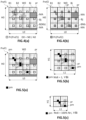
- a value difference is determined between corresponding reference pixels (pr) from the given reference image (Pref2) and a reference image (Pref1) (cf. Figure 1(a) ) preceding the given reference image (Pref2) in the sequence.
- a number (Nm) of motion pixels (pm) are selected (cf. black squares) whose value differences exceed a predefined threshold variation, indicative that the birds have moved within an area comprising the motion pixels.
- the reference image (Pref1) the given reference image (Pref2) is compared with can be a first image in a sequence of all images preceding the given image for which the triggering condition was not satisfied. For example, two successive reference images (Pref1, Pref2) are captured, and the values of their reference pixels (pr) are compared with one another. If no motion pixels (pm) or not enough motion pixels (pm) are identified to satisfy the triggering conditions, a third reference image (Pref3) and the values of its reference pixels (pr) are compared with the first reference image (Pref1), and so on until a movement is detected when the triggering conditions are satisfied. When the triggering conditions are fulfilled, the processing unit switches from the movement detection mode to the image capturing mode described in continuation.
- the processing unit is configured for first optimizing the properties of an output image (P1) to be captured, before capturing the output image (P1).
- the processing unit is configured for carrying out the following actions.
- the processing unit saves the predefined maximum output number N1m of pixels not to be exceeded by an output number (N1) of pixels defining the output image (P1) to be transferred out of the integrated circuit.
- the predefined maximum number (N1m) of pixels does not exceed the nominal number (N0) of pixels and is preferably smaller than the nominal number (N0) (i.e., N1 ⁇ N1m ⁇ N0, preferably N1 ⁇ N1m ⁇ N0). It is preferred that the processing unit be configured for allowing a modification of the maximum output number (N1m) of pixels by a user, as this parameter will affect the power consumption and resources required for operating the image capturing device.
- the output window (W1) defines the size and region of the output image (P1) to be captured.
- the processor is configured for controlling the array of N0 photosensors to capture the output image (P1) defined by the output window (W1) having the output window area (A1) and output pixel density (D1).
- the thus captured output image (P1) has not more than the predefined maximum output number N1m, which is important to limit the weight of the output image (P1) to be transferred.
- N1m predefined maximum output number
- the processing unit is configured for transferring the output image (P1) comprising N1 pixels out of the integrated circuit for further treatment.
- the integrated circuit comprises an array of a nominal number (N0) of photosensors. Each photosensor is configured for capturing a value of a corresponding pixel.
- the pixels form in combination an image. If the values of all photosensors of the array are used for forming the image, the image would be formed by N0 pixels and confined within a main window (W0) of output image area (A0).
- the resolution of the image is characterized by the pixel density.
- the pixel density of an image captured with the given array of photosensors can be less than D0, if less than N0 pixels form the image (e.g., by binning), but it cannot be higher, because there cannot be more than N0 pixels captured by N0 photosensors, and the size of each pixel is constant.
- An output mage (P1) with less than N0 pixels can be captured with a VGA.
- the output pixel density (D1) of the output image (P1) decreases as a result of such operations.
- the integrated circuit comprises a processing unit configured for first acting in a motion detection mode, configured for detecting whether a movement has occurred within the field defined by the main window (W0).
- the movement detection mode is also configured for detecting the region within the main window (W0) where the movement occurred. The movement detection mode is discussed in more details in continuation.
- the processing unit of the integrated circuit can switch to an image capture mode. Capturing a full-sized output image of main window area (A0) and nominal density (D0) is easy but transferring such a heavy output image (P1) out of the integrated circuit to an image processing unit consumes considerable energy and resources.
- the output image is sufficiently light for transfer out of the integrated circuit for further processing, as it is formed with N1 pixels only, yet with the highest possible resolution allowed by the predefined maximum output number (Nm1) of pixels, with D1 tending towards or even equalling the density N1m / A1.
- Nm1 N1m.
- the processing unit controls a subarray only of a number Nr of reference photosensors to capture a sequence of successive reference images (Prefj) at different times.
- Each reference image (Prefj) being defined by Nr corresponding reference pixels (pr).
- the number Nr of photosensors and reference pixels (pr) can be the same as the nominal number N0 of photosensors and pixels, but for sake of energy saving, it is preferred that Nr ⁇ N0 as shown in Figures 1(a) and 1(b) , where the reference pixels (pr) are represented with white and shaded squares.
- loop (g)-(g1)-(f) the processing unit can compare the values of the reference pixels (pr) between a given reference image (Pref1) and each successive reference image (Pref2) to detect any value difference exceeding a predefined threshold variation.
- loop (g)-(g2)-(f) the processing unit can compare a successive reference image (Pref2) with a preceding reference image (Pref1) preceding the successive reference image (Pref2) in the sequence of reference images (Pref1-Pref3) until a movement is detected.
- the reference pixels (pr) having values differing by more than the predefined threshold variation are identified and stored as motion pixels (pm).
- the reference pixels (pr) can be evenly distributed over the main window area (A0) or, alternatively, can be located at critical areas of the window (W0) where motions are expected. It is preferred that the processing unit is configured for allowing a modification of the number (Nr) and positions of the reference photosensors, depending on the specific application the image capturing device is allocated to.
- the value of the predefined threshold variation depends on the type of events expected to happen and can preferably also be modified by the user. For example, if the image capturing device is programmed for detecting movements of flying birds, the movements of leaves in surrounding trees should not be identified as movements, and the value variations associated with leaves moving should fall below the predefined threshold variation. The skilled person knows how to program the predefined threshold variation in order to only identify movements which are meaningful to the specific objectives of the image capturing device.
- the main window (W0) can comprise one or more masked portions (MA) as shown in Figures 4(a) and 4(b) .
- the masked portion (MA) comprise either,
- the processing unit is configured for passing from the movement detection mode to an image capture mode.
- the triggering condition can be considered as being satisfied if the number Nm of motion pixels (pm) is greater than or equal to a predefined lower triggering number (Ntd) (i.e., if 0 ⁇ Ntd ⁇ Nm).
- the triggering condition can be considered as being satisfied if the number Nm of motion pixels (pm) is lower than or equal to a predefined upper triggering number (Ntu) (i.e., if 0 ⁇ Ntd ⁇ Nm).
- the triggering conditions would be satisfied if 0 ⁇ Ntd ⁇ Nm ⁇ Ntu.
- the triggering conditions could be satisfied if the number (Nm) of motion pixels (pm) is comprised between 50% and 100%, preferably between 75% and 95%, or is preferably equal to 100% of the number Nr of reference pixels.
- the predefined lower triggering number (Ntd) can be required, for example, to prevent the processing unit from interpreting as a movement a change in a very limited number of reference pixels. For example, it may not be desirable to consider a branch in a corner of the main window (W0) moving with the wind as satisfying the triggering conditions.
- the predefined lower triggering number (Ntd) can be expressed as an absolute value (Ntd) of a lower boundary of the number Nm of motion pixels, below which the triggering condition is not fulfilled (i.e., Ntd ⁇ N ) .
- the predefined lower triggering number (Ntd) can be comprised between 50 and 100%, preferably between 70 and 95%, more preferably, between 75 and 80% of the number (Nr) of reference pixels (pr).
- the predefined upper triggering number (Ntu) can be required, for example, to prevent the processing unit from interpreting as a movement a sudden change of light (e.g., a light is switched on or off, or a dark cloud shades the sunlight) which would affect the signal of all reference pixels.
- the predefined upper triggering number (Ntu) can be expressed as an absolute value (Ntu) of an upper boundary of the number Nm of motion pixels, above which the triggering condition is not fulfilled (i.e., Ntu ⁇ N ).
- the predefined upper triggering number (Ntu) can be comprised between 75 and 100%, preferably between 85 and 98%, more preferably, between 90 and 95% of the number (Nr) of reference pixels (pr).
- the image sensor is divided into Nb photosensor blocks.
- Each photosensor block is formed by Ni adjacent photosensors.
- the blocks pave the whole main window area, without overlapping, such that each photosensor of the nominal number (N0) of photosensors forming the array belongs to one and only one photosensor block.
- Each one of the Nb photosensor blocks independently comprises a number Nri of block reference photosensors defined as the reference photosensors belonging to the block.
- An input image (P0) is similarly divided into Nb pixel blocks (Bi) corresponding to the Nb photosensor blocks, wherein each of the pixel blocks (Bi) comprises Nri reference pixels (pr).
- each pixel block (Bi) can therefore contain a block number Nmi of motion pixels (pm). All pixel blocks (Bi) need not necessarily have the same size, and the geometry of the pixel blocks can tailor the actual topography of the scene enclosed in the frame defined by the main window (W0).
- the advantage of dividing the main window (W0) into pixel blocks (Bi) is that it allows defining more targeted triggering conditions.
- the triggering conditions can be satisfied when the block number Nmi of motion pixels (pm) of at least one pixel block (Bi) is greater than or equal to a predefined lower block triggering number (Ntdi) (i.e., if 0 ⁇ Ntdi ⁇ Nmi).
- the triggering conditions can be satisfied when the block number Nmi of motion pixels (pmi) is lower than or equal to a predefined upper block triggering number (Ntui) (i.e., if 0 ⁇ Ntdi ⁇ Nmi).
- the triggering conditions would be satisfied if 0 ⁇ Ntdi ⁇ Nmi ⁇ Ntui.
- the predefined lower and upper triggering block numbers (Ntdi, Ntui) can be expressed as absolute values (Ntd, Ntu) of a lower and upper boundary of the number Nm of motion pixels in the block (i), below and above which the triggering condition is not fulfilled, respectively (i.e., Ntdi and Ntui ⁇ N ) .
- the predefined lower and upper triggering block numbers (Ntdi, Ntui) can have same values in all blocks (Bi), or can vary from one block (Bi) to another.
- each pixel block contains a single reference pixel (pr). It the value difference of the reference pixel (pr) of a given pixel block (Bi) exceeds the predefined threshold variation, the triggering condition is satisfied for the given block.
- the pixel blocks (Bi) can, however, contain one or more than one reference pixels (pr) (i.e., Nri ⁇ 1) and the number of reference pixels can be the same or different in two different pixel blocks. If a pixel block (Bi) contains more than one reference pixel (pr), the conditions to satisfy the triggering condition could vary. For example, as soon as a block contains one motion pixel (pm) the triggering condition is satisfied for this block (cf. Figure 5(b) ).
- a pixel block (Bi) must contain at least a predefined lower block triggering number (Ntdi) of motion pixels to satisfy the triggering conditions.
- the triggering condition could be satisfied for a given pixel block (Bi) only if all the reference pixels (pr) of the given block (Bi) are motion pixels (pm) (cf. Figure 5(c) ). It can be seen that dividing the main window (W0) in pixel blocks (Bi) gives an infinite variation of triggering conditions, which can be adapted to the specific topography and objective of the image capturing device.
- a finer and denser network of blocks (Bi) and / or of reference pixels (pr) can be concentrated in regions of the main window (W0) where events are expected with more probability.
- the main window comprises masked areas (MA)
- these can form one or more pixel blocks (Bi).
- the processing unit is preferably configured for generating an interrupt signal indicative of a switching into image capturing mode and of a coming output image (P1).
- the processing unit switches from the movement detection mode to the image capturing mode.
- the processing unit is configured for generating an interrupt signal indicative that a movement detected in a region of the main window and of a switching into the image capturing mode.
- This optimisation process is carried out within the integrated circuit, priorto capturing the output image (P1) and of course, prior to transferring it outside of the integrated circuit for further treatments.
- This solution leads to considerable energy saving and requires less processing resources as the weight of the output image (i.e., the output number (N1) of pixels is restricted to not more than the predefined maximum number (N1m) of pixels, i.e., N1 ⁇ N1m).
- the output area (A1) of the output image (W1) and the output number (N1) of pixels can be optimised in different ways. For example, they can be optimised by satisfying one or more of the following criteria.
- the output window (W0) can be selected according to different criteria.
- nL is independent of nH and could have different values (i.e., nH ⁇ nL is possible).
- nH and nL both or each independently have a value selected among preselected values of 1, 1/2, 1/3, or 1/4.
- the length (L1) and height (H1) of the output window (W1) can be selected among a predefined set of output image window lengths (L1) and heights (H1).
- the output window (W1) must enclose at least a predefined fraction of thenumber (Nm) of motion pixels (pm). This allows focusing the output window (W1) in a region of the main window (W0) where events occurred with movement detected therein.
- the processing unit can be configured to ensure that the output window (W1) encloses a number of motion pixels comprised between 50% and 100%, preferably between 75% and 95%, or is preferably equal to 100% of the number (Nm) of motion pixels (pm).
- the processing unit can be configured to enclose in the output window (W1) only the motion pixels comprising at least one or two, or more direct neighbouring reference pixels (pr) which are also motion pixels (pm). This would avoid including portions of the main window (W0) where only minimal motion occurred, as indicated by the fact that a single (isolated) reference pixel (pr) varied to become a motion pixel (pm) in that portion of W0.
- the output window (W1) can be limited to an output window area (A1) greater than or equal to a predefined minimum output window area (A1min), such that 0 ⁇ A1min ⁇ A1 ⁇ A0. This allows avoiding selecting an output window (W1) of too small dimensions to capture a wide enough frame to have a large enough general view of the scene (see for example, Figure 2(b) which shows only a fraction of both large and small birds).
- the output window (W1) may enclose all the blocks (Bi) satisfying different criteria.
- the output window (W1) may enclose all the blocks (Bi) satisfying different criteria.
- one reference pixel (pr) of a pixel block (Bi) be identified as a motion pixel (pm)
- the whole pixel block (Bi) to be enclosed within the output image (W0)
- the pixel block (Bi) comprises other reference pixels (pr) which are not motion pixels (pm).
- a pixel block may require that all the reference pixels contained therein be identified as motion pixels (pm) as illustrated in Figure 5(c) .
- a pixel block (Bi) can be included within the output window (W0) as soon as at least a predefined fraction of the reference pixels (pr) be identified as motion pixels, such as at least 50% of the reference pixels (pr), preferably at least 67% or 75% of the reference pixels (pr).
- the processing unit is configured for determining the output number of pixels (N1) for optimizing the resolution of the output image (P1) satisfying the condition of not exceeding the predefined maximum output number (N1m) of pixels. This process is described in continuation.
- the processing unit of the integrated circuit is configured for maximising the output pixel density (D1) whilst maintaining the output number (N1) of pixels below or equal to the predefined maximum output number (N1m) of pixels.
- N1 n N0
- the number proportionality factor m must be reduced to less than the area proportionality factor n (i.e., m ⁇ n), until N1 ⁇ N1m.
- N1 of pixels Reducing the output number (N1) of pixels, however, cannot be done arbitrarily.
- Two common ways of reducing the output number (N1) of pixels for an output image (W1) of given output image area (A1) include decimation and aggregation (or binning). In decimation, only a pixel in every block of 2 ⁇ 2, 4x4, etc. pixels is read. Information contained in all the unread pixels is therefore lost. To avoid losing information, pixels can be "connected" together in order to average their signal in a process called aggregation or binning.
- the processing unit of the present invention can be programmed for reducing the output number (N1) of pixels by either aggregation or decimation. Aggregation is, however, preferred, as losing completely the information of the unread pixels is not ideal in many applications.
- the processing unit can be configured for maximizing the A1 / A0 ratio and for maximizing the product D1 ⁇ A1 as follows.
- the output pixel density (D1) cannot always be reduced by any arbitrary value of the factor m, without distorting the output image.
- aggregation or binning
- the processing unit can be configured for performing two alternative options.
- n 50%
- N1 N1m
- N0 %
- N1m N0 / 4
- Nm the number of motion pixels
- This further operation has the advantage of increasing the field of the output image without decreasing the resolution thereof and still fulfilling the condition on N1 ⁇ N1m.
- the additional pixels can be added by adding successive lines of pixels of length (L1), or successive columns of pixels of height (H1), or both, thus homothetically increasing the output window area (A1) of the output window (W1).
- N1 m N0 ⁇ N0
- N1 n N0 ⁇ N1m.
- N1 n N0 > N1m, yielding an output image (P0) which is too heavy to export.
- the processing unit is configured for maximizing the product A1 ⁇ D1 (cf. Figure 7(m) ).
- the processing unit of the integrated circuit is configured for controlling the array of photosensors to capture the output image (P1). Once captured, the output image can be exported for further treatment. Since the weight of the output image (P1) is limited to not more than N1m pixels, the power consumed for the transfer are minimized by avoiding a transfer of a large and dense frame, reducing also the processing resources required for the transfer of the output image.
- the gist of the present invention is to move the processing to select the area of interest to the integrated circuit prior to exporting the output image (P1), rather than capturing a full-size output image (P1) and re-framing it in a separate image treatment unit after transfer of the output image thereto.
- the present invention also concerns an image capture and treatment device comprising the integrated circuit as defined supra, a lens in optical communication with the array of N0 photosensors of the image sensor of the integrated circuit, and an image treatment unit in communication with the integrated circuit and configured for receiving and preferably saving the output images (P1) from the integrated circuit.
- the image treatment unit is preferably configured for receiving an interrupt signal generated by the processing unit of the integrated circuit, which is indicative of a coming output image (P1). Upon receiving the interrupt signal, the image treatment unit can switch from a sleep mode of the image treatment unit to a wake-up mode of the image treatment unit.
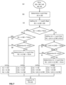
- Figure 6 shows a flowchart explaining the various operations the processing unit of the integrated circuit of the present invention is configured for carrying out.
- the processing unit stores the value of the predefined maximum output number N1m ⁇ N0 of pixels not to be exceeded by an output number (N1) of pixels defining the output image (P1) to be transferred out of the integrated circuit (i.e., N1 ⁇ N1m ⁇ N0), (cf. Figure 6 , boxes (a)&(b)).
- the subarray of reference pixels (pr) must be defined as shown in Figure 6 , box (c)).
- the processing unit is configured for capturing a sequence of successive reference images (Pref1, Pref2) at different times/ (cf. Figure 6 , boxes (d)&(e)).
- the reference pixels (pr) satisfying the criteria for being considered as motion pixels (pm) are identified, and the processing unit checks whether the triggering conditions are fulfilled by the motion pixels (pm) to conclude that there has been a movement between a first and second reference images (Pref1, Pref2) (cf. Figure 6 , boxes (f)&(g)).
- the processing unit captures a next reference image (Pref3).
- the processing unit repeats steps (f)&(g)), comparing the next reference image (Pref3) with the first reference image (Pref1) until the triggering conditions are satisfied, and a movement has been detected.
- the next reference image (Pref3) is compared with the preceding reference image (Pref2) and the processing unit repeats steps (f)&(g) by replacing the first reference image (Pref1) by the second reference image (Pref2) for the sake of comparisons, and so on until the triggering conditions are satisfied, and a movement has been detected.
- the processing unit then passes in image capture mode, wherein the parameters of the output image (P1) to be captured are first optimized. before capturing the output image (cf. Figure 6 , box (h)).
- the output window (W1) and output image area (A1) are defined, focusing on the region of the main window (W0) where the movement occurred.
- the processing unit is configured for capturing the output image (P1) with said parameters, and for transferring the output image (P1) out of the integrated circuit for further treatment or analysis (cf. Figure 6 , boxes (i)&(j)).
- the processing unit is then ready for passing in movement detection mode again, and capturing a new sequence of successive reference images (Pref1; Pref2) at different times and repeating the foregoing steps (cf. Figure 6 , loop between boxes (j) and (d)).
Landscapes
- Engineering & Computer Science (AREA)
- Multimedia (AREA)
- Signal Processing (AREA)
- Transforming Light Signals Into Electric Signals (AREA)
- Image Analysis (AREA)
- Studio Devices (AREA)
Priority Applications (7)
| Application Number | Priority Date | Filing Date | Title |
|---|---|---|---|
| EP23150997.7A EP4401418A1 (de) | 2023-01-10 | 2023-01-10 | Vorrichtung und verfahren für automatisierte ausgabe eines bildbewegungsbereichs |
| TW112149295A TW202429901A (zh) | 2023-01-10 | 2023-12-18 | 用於自動放大運動區之設備及方法 |
| EP24700252.0A EP4649688A1 (de) | 2023-01-10 | 2024-01-09 | Integrierte schaltung zur optimierung eines automatisierten zooms im bewegungsbereich eines bildes |
| PCT/EP2024/050351 WO2024149733A1 (en) | 2023-01-10 | 2024-01-09 | Integrated circuit for optimizing automated zoom in motion area of image |
| KR1020257026457A KR20250134641A (ko) | 2023-01-10 | 2024-01-09 | 이미지의 모션 영역에서 자동 줌을 최적화하기 위한 집적 회로 |
| JP2025539828A JP2026501729A (ja) | 2023-01-10 | 2024-01-09 | 画像の運動エリア内の自動ズームを最適化するための集積回路 |
| CN202480015026.5A CN120826913A (zh) | 2023-01-10 | 2024-01-09 | 用于优化图像的自动放大运动区的集成电路 |
Applications Claiming Priority (1)
| Application Number | Priority Date | Filing Date | Title |
|---|---|---|---|
| EP23150997.7A EP4401418A1 (de) | 2023-01-10 | 2023-01-10 | Vorrichtung und verfahren für automatisierte ausgabe eines bildbewegungsbereichs |
Publications (1)
| Publication Number | Publication Date |
|---|---|
| EP4401418A1 true EP4401418A1 (de) | 2024-07-17 |
Family
ID=84901695
Family Applications (2)
| Application Number | Title | Priority Date | Filing Date |
|---|---|---|---|
| EP23150997.7A Withdrawn EP4401418A1 (de) | 2023-01-10 | 2023-01-10 | Vorrichtung und verfahren für automatisierte ausgabe eines bildbewegungsbereichs |
| EP24700252.0A Pending EP4649688A1 (de) | 2023-01-10 | 2024-01-09 | Integrierte schaltung zur optimierung eines automatisierten zooms im bewegungsbereich eines bildes |
Family Applications After (1)
| Application Number | Title | Priority Date | Filing Date |
|---|---|---|---|
| EP24700252.0A Pending EP4649688A1 (de) | 2023-01-10 | 2024-01-09 | Integrierte schaltung zur optimierung eines automatisierten zooms im bewegungsbereich eines bildes |
Country Status (6)
| Country | Link |
|---|---|
| EP (2) | EP4401418A1 (de) |
| JP (1) | JP2026501729A (de) |
| KR (1) | KR20250134641A (de) |
| CN (1) | CN120826913A (de) |
| TW (1) | TW202429901A (de) |
| WO (1) | WO2024149733A1 (de) |
Citations (14)
| Publication number | Priority date | Publication date | Assignee | Title |
|---|---|---|---|---|
| KR20040024888A (ko) * | 2002-09-17 | 2004-03-24 | (주)펜타마이크로 | 시간 필터링을 이용한 영상잡음 제거시 움직임 검출 장치및 그 방법 |
| US20060262958A1 (en) * | 2005-05-19 | 2006-11-23 | Objectvideo, Inc. | Periodic motion detection with applications to multi-grabbing |
| US7279671B2 (en) | 2005-02-03 | 2007-10-09 | Olympus Corporation | Image acquisition apparatus for use with a microscope including detection of the amount of change between and image and a subsequent image, and an image recording system that use the image acquisition apparatus |
| US20090109290A1 (en) * | 2007-10-25 | 2009-04-30 | Bo Ye | Motion-Adaptive Alternate Gamma Drive for LCD |
| US20090219387A1 (en) * | 2008-02-28 | 2009-09-03 | Videolq, Inc. | Intelligent high resolution video system |
| US20130162759A1 (en) * | 2011-12-23 | 2013-06-27 | Nokia Corporation | Controlling Image Capture and/or Controlling Image Processing |
| US20130187027A1 (en) * | 2012-01-20 | 2013-07-25 | Omnivision Technologies, Inc. | Image sensor with integrated ambient light detection |
| US20140118592A1 (en) | 2012-10-26 | 2014-05-01 | The Regents Of The University Of Michigan | Cmos image sensors with feature extraction |
| US20150326784A1 (en) * | 2014-05-09 | 2015-11-12 | Canon Kabushiki Kaisha | Image capturing control method and image pickup apparatus |
| CN106657780A (zh) | 2016-12-16 | 2017-05-10 | 北京小米移动软件有限公司 | 图像预览方法和装置 |
| US11025822B2 (en) | 2016-08-01 | 2021-06-01 | Sony Corporation | Imaging apparatus and control method for imaging apparatus |
| US20210185266A1 (en) * | 2019-12-13 | 2021-06-17 | Sony Semiconductor Solutions Corporation | Methods and systems of low power facial recognition |
| US11218641B2 (en) | 2019-09-09 | 2022-01-04 | Qualcomm Incorporated | Image capture mode adaptation |
| US20220141409A1 (en) | 2019-07-19 | 2022-05-05 | Canon Kabushiki Kaisha | Imaging apparatus and control method thereof |
Family Cites Families (1)
| Publication number | Priority date | Publication date | Assignee | Title |
|---|---|---|---|---|
| US6541751B1 (en) * | 2001-10-03 | 2003-04-01 | Pixim Inc | Time multiplexing image processing functions for noise reduction |
-
2023
- 2023-01-10 EP EP23150997.7A patent/EP4401418A1/de not_active Withdrawn
- 2023-12-18 TW TW112149295A patent/TW202429901A/zh unknown
-
2024
- 2024-01-09 KR KR1020257026457A patent/KR20250134641A/ko active Pending
- 2024-01-09 WO PCT/EP2024/050351 patent/WO2024149733A1/en not_active Ceased
- 2024-01-09 JP JP2025539828A patent/JP2026501729A/ja active Pending
- 2024-01-09 EP EP24700252.0A patent/EP4649688A1/de active Pending
- 2024-01-09 CN CN202480015026.5A patent/CN120826913A/zh active Pending
Patent Citations (15)
| Publication number | Priority date | Publication date | Assignee | Title |
|---|---|---|---|---|
| KR20040024888A (ko) * | 2002-09-17 | 2004-03-24 | (주)펜타마이크로 | 시간 필터링을 이용한 영상잡음 제거시 움직임 검출 장치및 그 방법 |
| US7279671B2 (en) | 2005-02-03 | 2007-10-09 | Olympus Corporation | Image acquisition apparatus for use with a microscope including detection of the amount of change between and image and a subsequent image, and an image recording system that use the image acquisition apparatus |
| US20080007821A1 (en) * | 2005-02-03 | 2008-01-10 | Hironori Kishida | Image acquisition apparatus for use with a microscope, an image recording system that uses the image acquisition apparatus, and an image storage method |
| US20060262958A1 (en) * | 2005-05-19 | 2006-11-23 | Objectvideo, Inc. | Periodic motion detection with applications to multi-grabbing |
| US20090109290A1 (en) * | 2007-10-25 | 2009-04-30 | Bo Ye | Motion-Adaptive Alternate Gamma Drive for LCD |
| US20090219387A1 (en) * | 2008-02-28 | 2009-09-03 | Videolq, Inc. | Intelligent high resolution video system |
| US20130162759A1 (en) * | 2011-12-23 | 2013-06-27 | Nokia Corporation | Controlling Image Capture and/or Controlling Image Processing |
| US20130187027A1 (en) * | 2012-01-20 | 2013-07-25 | Omnivision Technologies, Inc. | Image sensor with integrated ambient light detection |
| US20140118592A1 (en) | 2012-10-26 | 2014-05-01 | The Regents Of The University Of Michigan | Cmos image sensors with feature extraction |
| US20150326784A1 (en) * | 2014-05-09 | 2015-11-12 | Canon Kabushiki Kaisha | Image capturing control method and image pickup apparatus |
| US11025822B2 (en) | 2016-08-01 | 2021-06-01 | Sony Corporation | Imaging apparatus and control method for imaging apparatus |
| CN106657780A (zh) | 2016-12-16 | 2017-05-10 | 北京小米移动软件有限公司 | 图像预览方法和装置 |
| US20220141409A1 (en) | 2019-07-19 | 2022-05-05 | Canon Kabushiki Kaisha | Imaging apparatus and control method thereof |
| US11218641B2 (en) | 2019-09-09 | 2022-01-04 | Qualcomm Incorporated | Image capture mode adaptation |
| US20210185266A1 (en) * | 2019-12-13 | 2021-06-17 | Sony Semiconductor Solutions Corporation | Methods and systems of low power facial recognition |
Also Published As
| Publication number | Publication date |
|---|---|
| WO2024149733A1 (en) | 2024-07-18 |
| JP2026501729A (ja) | 2026-01-16 |
| EP4649688A1 (de) | 2025-11-19 |
| KR20250134641A (ko) | 2025-09-11 |
| TW202429901A (zh) | 2024-07-16 |
| CN120826913A (zh) | 2025-10-21 |
Similar Documents
| Publication | Publication Date | Title |
|---|---|---|
| EP3997866B1 (de) | System und verfahren zur inhaltsverbesserung mittels vierfarbfilteranordnungssensoren | |
| US8576293B2 (en) | Multi-channel imager | |
| US6680748B1 (en) | Multi-mode camera and method therefor | |
| US9066032B2 (en) | Imaging apparatus comprising image sensor array having shared global shutter circuitry | |
| DE10323236B4 (de) | Bilderzeugungsvorrichtung | |
| JP2021052396A (ja) | 複数のイメージセンサにより獲得されるイメージデータに基づいてビデオhdr処理を遂行するための電子装置 | |
| KR102943206B1 (ko) | 장치, 이것의 제어방법, 및 기억매체 | |
| US8564640B2 (en) | Systems and methods of creating a virtual window | |
| DE112020006102T5 (de) | Verfahren und system zur gesichtserkennung mit geringer leistungsaufnahme | |
| US20180183998A1 (en) | Power reduction and performance improvement through selective sensor image downscaling | |
| CN107534742A (zh) | 成像方法、图像传感器以及成像设备 | |
| US10477137B2 (en) | Array camera imaging system having distributed memory | |
| US20240259686A1 (en) | Imaging apparatus | |
| DE602005003497T2 (de) | Mobiles Gerät mit Bildsensoren zum Laden einer Batterie | |
| CN103106638A (zh) | 用于实时图像处理的图形处理装置 | |
| EP4401418A1 (de) | Vorrichtung und verfahren für automatisierte ausgabe eines bildbewegungsbereichs | |
| EP1829361A1 (de) | Verfahren zum extrahieren mehrerer subfenster eines abtastbereichs mittels einer digitalen videokamera | |
| GB2417382A (en) | Camera with scaleable resolution | |
| CN111131714A (zh) | 图像采集控制方法、装置及电子设备 | |
| US11924555B2 (en) | Intelligent auto-exposure control for RGB-IR sensor | |
| CN113965687B (zh) | 拍摄方法、装置和电子设备 | |
| JP7325211B2 (ja) | 撮像装置及びその制御方法、プログラム、記憶媒体 | |
| US12542877B1 (en) | Image signal processor motion detector | |
| US12316985B2 (en) | Image sensor including image signal processor and operating method of the image sensor | |
| US10091441B1 (en) | Image capture at multiple resolutions |
Legal Events
| Date | Code | Title | Description |
|---|---|---|---|
| PUAI | Public reference made under article 153(3) epc to a published international application that has entered the european phase |
Free format text: ORIGINAL CODE: 0009012 |
|
| STAA | Information on the status of an ep patent application or granted ep patent |
Free format text: STATUS: THE APPLICATION HAS BEEN PUBLISHED |
|
| AK | Designated contracting states |
Kind code of ref document: A1 Designated state(s): AL AT BE BG CH CY CZ DE DK EE ES FI FR GB GR HR HU IE IS IT LI LT LU LV MC ME MK MT NL NO PL PT RO RS SE SI SK SM TR |
|
| STAA | Information on the status of an ep patent application or granted ep patent |
Free format text: STATUS: THE APPLICATION IS DEEMED TO BE WITHDRAWN |
|
| 18D | Application deemed to be withdrawn |
Effective date: 20250118 |