EP4401116A2 - Staircase structure in three-dimensional memory device and method for forming the same - Google Patents
Staircase structure in three-dimensional memory device and method for forming the same Download PDFInfo
- Publication number
- EP4401116A2 EP4401116A2 EP24177978.4A EP24177978A EP4401116A2 EP 4401116 A2 EP4401116 A2 EP 4401116A2 EP 24177978 A EP24177978 A EP 24177978A EP 4401116 A2 EP4401116 A2 EP 4401116A2
- Authority
- EP
- European Patent Office
- Prior art keywords
- dielectric
- conductor
- stair
- sacrificial
- staircase
- Prior art date
- Legal status (The legal status is an assumption and is not a legal conclusion. Google has not performed a legal analysis and makes no representation as to the accuracy of the status listed.)
- Pending
Links
Images






Classifications
-
- H—ELECTRICITY
- H10—SEMICONDUCTOR DEVICES; ELECTRIC SOLID-STATE DEVICES NOT OTHERWISE PROVIDED FOR
- H10P—GENERIC PROCESSES OR APPARATUS FOR THE MANUFACTURE OR TREATMENT OF DEVICES COVERED BY CLASS H10
- H10P50/00—Etching of wafers, substrates or parts of devices
- H10P50/20—Dry etching; Plasma etching; Reactive-ion etching
- H10P50/28—Dry etching; Plasma etching; Reactive-ion etching of insulating materials
- H10P50/282—Dry etching; Plasma etching; Reactive-ion etching of insulating materials of inorganic materials
- H10P50/283—Dry etching; Plasma etching; Reactive-ion etching of insulating materials of inorganic materials by chemical means
-
- H—ELECTRICITY
- H10—SEMICONDUCTOR DEVICES; ELECTRIC SOLID-STATE DEVICES NOT OTHERWISE PROVIDED FOR
- H10W—GENERIC PACKAGES, INTERCONNECTIONS, CONNECTORS OR OTHER CONSTRUCTIONAL DETAILS OF DEVICES COVERED BY CLASS H10
- H10W20/00—Interconnections in chips, wafers or substrates
- H10W20/40—Interconnections external to wafers or substrates, e.g. back-end-of-line [BEOL] metallisations or vias connecting to gate electrodes
- H10W20/41—Interconnections external to wafers or substrates, e.g. back-end-of-line [BEOL] metallisations or vias connecting to gate electrodes characterised by their conductive parts
- H10W20/435—Cross-sectional shapes or dispositions of interconnections
-
- H—ELECTRICITY
- H10—SEMICONDUCTOR DEVICES; ELECTRIC SOLID-STATE DEVICES NOT OTHERWISE PROVIDED FOR
- H10B—ELECTRONIC MEMORY DEVICES
- H10B41/00—Electrically erasable-and-programmable ROM [EEPROM] devices comprising floating gates
- H10B41/10—Electrically erasable-and-programmable ROM [EEPROM] devices comprising floating gates characterised by the top-view layout
-
- H—ELECTRICITY
- H10—SEMICONDUCTOR DEVICES; ELECTRIC SOLID-STATE DEVICES NOT OTHERWISE PROVIDED FOR
- H10B—ELECTRONIC MEMORY DEVICES
- H10B41/00—Electrically erasable-and-programmable ROM [EEPROM] devices comprising floating gates
- H10B41/20—Electrically erasable-and-programmable ROM [EEPROM] devices comprising floating gates characterised by three-dimensional [3D] arrangements, e.g. with cells on different height levels
-
- H—ELECTRICITY
- H10—SEMICONDUCTOR DEVICES; ELECTRIC SOLID-STATE DEVICES NOT OTHERWISE PROVIDED FOR
- H10B—ELECTRONIC MEMORY DEVICES
- H10B41/00—Electrically erasable-and-programmable ROM [EEPROM] devices comprising floating gates
- H10B41/20—Electrically erasable-and-programmable ROM [EEPROM] devices comprising floating gates characterised by three-dimensional [3D] arrangements, e.g. with cells on different height levels
- H10B41/23—Electrically erasable-and-programmable ROM [EEPROM] devices comprising floating gates characterised by three-dimensional [3D] arrangements, e.g. with cells on different height levels with source and drain on different levels, e.g. with sloping channels
- H10B41/27—Electrically erasable-and-programmable ROM [EEPROM] devices comprising floating gates characterised by three-dimensional [3D] arrangements, e.g. with cells on different height levels with source and drain on different levels, e.g. with sloping channels the channels comprising vertical portions, e.g. U-shaped channels
-
- H—ELECTRICITY
- H10—SEMICONDUCTOR DEVICES; ELECTRIC SOLID-STATE DEVICES NOT OTHERWISE PROVIDED FOR
- H10B—ELECTRONIC MEMORY DEVICES
- H10B41/00—Electrically erasable-and-programmable ROM [EEPROM] devices comprising floating gates
- H10B41/30—Electrically erasable-and-programmable ROM [EEPROM] devices comprising floating gates characterised by the memory core region
- H10B41/35—Electrically erasable-and-programmable ROM [EEPROM] devices comprising floating gates characterised by the memory core region with a cell select transistor, e.g. NAND
-
- H—ELECTRICITY
- H10—SEMICONDUCTOR DEVICES; ELECTRIC SOLID-STATE DEVICES NOT OTHERWISE PROVIDED FOR
- H10B—ELECTRONIC MEMORY DEVICES
- H10B41/00—Electrically erasable-and-programmable ROM [EEPROM] devices comprising floating gates
- H10B41/50—Electrically erasable-and-programmable ROM [EEPROM] devices comprising floating gates characterised by the boundary region between the core region and the peripheral circuit region
-
- H—ELECTRICITY
- H10—SEMICONDUCTOR DEVICES; ELECTRIC SOLID-STATE DEVICES NOT OTHERWISE PROVIDED FOR
- H10B—ELECTRONIC MEMORY DEVICES
- H10B43/00—EEPROM devices comprising charge-trapping gate insulators
- H10B43/10—EEPROM devices comprising charge-trapping gate insulators characterised by the top-view layout
-
- H—ELECTRICITY
- H10—SEMICONDUCTOR DEVICES; ELECTRIC SOLID-STATE DEVICES NOT OTHERWISE PROVIDED FOR
- H10B—ELECTRONIC MEMORY DEVICES
- H10B43/00—EEPROM devices comprising charge-trapping gate insulators
- H10B43/20—EEPROM devices comprising charge-trapping gate insulators characterised by three-dimensional [3D] arrangements, e.g. with cells on different height levels
-
- H—ELECTRICITY
- H10—SEMICONDUCTOR DEVICES; ELECTRIC SOLID-STATE DEVICES NOT OTHERWISE PROVIDED FOR
- H10B—ELECTRONIC MEMORY DEVICES
- H10B43/00—EEPROM devices comprising charge-trapping gate insulators
- H10B43/20—EEPROM devices comprising charge-trapping gate insulators characterised by three-dimensional [3D] arrangements, e.g. with cells on different height levels
- H10B43/23—EEPROM devices comprising charge-trapping gate insulators characterised by three-dimensional [3D] arrangements, e.g. with cells on different height levels with source and drain on different levels, e.g. with sloping channels
- H10B43/27—EEPROM devices comprising charge-trapping gate insulators characterised by three-dimensional [3D] arrangements, e.g. with cells on different height levels with source and drain on different levels, e.g. with sloping channels the channels comprising vertical portions, e.g. U-shaped channels
-
- H—ELECTRICITY
- H10—SEMICONDUCTOR DEVICES; ELECTRIC SOLID-STATE DEVICES NOT OTHERWISE PROVIDED FOR
- H10B—ELECTRONIC MEMORY DEVICES
- H10B43/00—EEPROM devices comprising charge-trapping gate insulators
- H10B43/30—EEPROM devices comprising charge-trapping gate insulators characterised by the memory core region
- H10B43/35—EEPROM devices comprising charge-trapping gate insulators characterised by the memory core region with cell select transistors, e.g. NAND
-
- H—ELECTRICITY
- H10—SEMICONDUCTOR DEVICES; ELECTRIC SOLID-STATE DEVICES NOT OTHERWISE PROVIDED FOR
- H10B—ELECTRONIC MEMORY DEVICES
- H10B43/00—EEPROM devices comprising charge-trapping gate insulators
- H10B43/50—EEPROM devices comprising charge-trapping gate insulators characterised by the boundary region between the core and peripheral circuit regions
-
- H—ELECTRICITY
- H10—SEMICONDUCTOR DEVICES; ELECTRIC SOLID-STATE DEVICES NOT OTHERWISE PROVIDED FOR
- H10D—INORGANIC ELECTRIC SEMICONDUCTOR DEVICES
- H10D84/00—Integrated devices formed in or on semiconductor substrates that comprise only semiconducting layers, e.g. on Si wafers or on GaAs-on-Si wafers
- H10D84/01—Manufacture or treatment
- H10D84/0123—Integrating together multiple components covered by H10D12/00 or H10D30/00, e.g. integrating multiple IGBTs
- H10D84/0126—Integrating together multiple components covered by H10D12/00 or H10D30/00, e.g. integrating multiple IGBTs the components including insulated gates, e.g. IGFETs
- H10D84/0149—Manufacturing their interconnections or electrodes, e.g. source or drain electrodes
-
- H—ELECTRICITY
- H10—SEMICONDUCTOR DEVICES; ELECTRIC SOLID-STATE DEVICES NOT OTHERWISE PROVIDED FOR
- H10W—GENERIC PACKAGES, INTERCONNECTIONS, CONNECTORS OR OTHER CONSTRUCTIONAL DETAILS OF DEVICES COVERED BY CLASS H10
- H10W20/00—Interconnections in chips, wafers or substrates
- H10W20/01—Manufacture or treatment
- H10W20/031—Manufacture or treatment of conductive parts of the interconnections
- H10W20/056—Manufacture or treatment of conductive parts of the interconnections by filling conductive material into holes, grooves or trenches
-
- H—ELECTRICITY
- H10—SEMICONDUCTOR DEVICES; ELECTRIC SOLID-STATE DEVICES NOT OTHERWISE PROVIDED FOR
- H10W—GENERIC PACKAGES, INTERCONNECTIONS, CONNECTORS OR OTHER CONSTRUCTIONAL DETAILS OF DEVICES COVERED BY CLASS H10
- H10W20/00—Interconnections in chips, wafers or substrates
- H10W20/01—Manufacture or treatment
- H10W20/071—Manufacture or treatment of dielectric parts thereof
- H10W20/081—Manufacture or treatment of dielectric parts thereof by forming openings in the dielectric parts
- H10W20/089—Manufacture or treatment of dielectric parts thereof by forming openings in the dielectric parts using processes for implementing desired shapes or dispositions of the openings, e.g. double patterning
-
- H—ELECTRICITY
- H10—SEMICONDUCTOR DEVICES; ELECTRIC SOLID-STATE DEVICES NOT OTHERWISE PROVIDED FOR
- H10W—GENERIC PACKAGES, INTERCONNECTIONS, CONNECTORS OR OTHER CONSTRUCTIONAL DETAILS OF DEVICES COVERED BY CLASS H10
- H10W20/00—Interconnections in chips, wafers or substrates
- H10W20/01—Manufacture or treatment
- H10W20/071—Manufacture or treatment of dielectric parts thereof
- H10W20/093—Manufacture or treatment of dielectric parts thereof by modifying materials of the dielectric parts
- H10W20/095—Manufacture or treatment of dielectric parts thereof by modifying materials of the dielectric parts by irradiating with electromagnetic or particle radiation
-
- H—ELECTRICITY
- H10—SEMICONDUCTOR DEVICES; ELECTRIC SOLID-STATE DEVICES NOT OTHERWISE PROVIDED FOR
- H10W—GENERIC PACKAGES, INTERCONNECTIONS, CONNECTORS OR OTHER CONSTRUCTIONAL DETAILS OF DEVICES COVERED BY CLASS H10
- H10W20/00—Interconnections in chips, wafers or substrates
- H10W20/40—Interconnections external to wafers or substrates, e.g. back-end-of-line [BEOL] metallisations or vias connecting to gate electrodes
- H10W20/41—Interconnections external to wafers or substrates, e.g. back-end-of-line [BEOL] metallisations or vias connecting to gate electrodes characterised by their conductive parts
- H10W20/42—Vias, e.g. via plugs
Definitions
- Embodiments of the present disclosure relate to three-dimensional (3D) memory devices and fabrication methods thereof.
- Planar memory cells are scaled to smaller sizes by improving process technology, circuit design, programming algorithm, and fabrication process.
- feature sizes of the memory cells approach a lower limit
- planar process and fabrication techniques become challenging and costly.
- memory density for planar memory cells approaches an upper limit.
- a 3D memory architecture can address the density limitation in planar memory cells.
- the 3D memory architecture includes a memory array and peripheral devices for controlling signals to and from the memory array.
- Embodiments of 3D memory devices having staircase structures and methods for forming the same are disclosed herein.
- the 3D memory device includes a memory array structure and a staircase structure.
- the staircase structure is located in an intermediate of the memory array structure and divides the memory array structure into a first memory array structure and a second memory array structure along a lateral direction.
- the staircase structure includes a plurality of stairs extending along the lateral direction, and a bridge structure in contact with the first memory array structure and the second memory array structure.
- the plurality of stairs includes a stair above one or more dielectric pairs.
- the stair includes a conductor portion on a top surface of the stair and in contact with and electrically connected to the bridge structure, and a dielectric portion at a same level and in contact with the conductor portion.
- the stair is electrically connected to at least one of the first memory array structure and the second memory array structure through the bridge structure.
- a width of the conductor portion decreases.
- the 3D memory device includes a memory array structure and a landing structure in contact with the memory array structure.
- the landing structure includes a plurality of landing areas each at a respective depth extending along a lateral direction, and a bridge structure in contact with the memory array structure.
- the plurality of landing areas each includes a conductor portion on a respective top surface and a dielectric portion at a same level and in contact with the conductor portion.
- the conductor portion is electrically connected to the memory array structure through the bridge structure.
- a width of the conductor portion decreases along a second lateral direction perpendicular to the lateral direction and away from the bridge structure.
- the plurality of landing areas are each above one or more dielectric pairs.
- the 3D memory device includes a memory array structure and a staircase structure.
- the staircase structure includes a plurality of stairs extending along a lateral direction.
- the plurality of stairs includes a stair having a conductor portion on a top surface of the stair and a dielectric portion at a same level and in contact with the conductor portion.
- the conduction portion is electrically connected to the memory array structure.
- a width of the conductor portion varies.
- a method for forming a staircase structure of 3D memory device includes the following operations. First, a plurality of stairs are formed having interleaved a plurality of first sacrificial layers and a plurality of first dielectric layers in a plurality of stairs. A bridge structure is formed in contact with the plurality of stairs, the bridge structure having interleaved a plurality of second sacrificial layers and a plurality of second dielectric layers. Each first sacrificial layer is in contact with a respective second sacrificial layer of the same level, and each first dielectric layer is in contact with a respective second dielectric layer of the same level.
- references in the specification to "one embodiment,” “an embodiment,” “an example embodiment,” “some embodiments,” etc. indicate that the embodiment described may include a particular feature, structure, or characteristic, but every embodiment may not necessarily include the particular feature, structure, or characteristic. Moreover, such phrases do not necessarily refer to the same embodiment. Further, when a particular feature, structure or characteristic is described in connection with an embodiment, it would be within the knowledge of a person skilled in the pertinent art to effect such feature, structure or characteristic in connection with other embodiments whether or not explicitly described.
- spatially relative terms such as “beneath,” “below,” “lower,” “above,” “upper,” and the like, may be used herein for ease of description to describe one element or feature's relationship to another element(s) or feature(s) as illustrated in the figures.
- the spatially relative terms are intended to encompass different orientations of the device in use or operation in addition to the orientation depicted in the figures.
- the apparatus may be otherwise oriented (rotated 90 degrees or at other orientations), and the spatially relative descriptors used herein may likewise be interpreted accordingly.
- the term "substrate” refers to a material onto which subsequent material layers are added.
- the substrate itself can be patterned. Materials added on top of the substrate can be patterned or can remain unpatterned.
- the substrate can include a wide array of semiconductor materials, such as silicon, germanium, gallium arsenide, indium phosphide, etc.
- the substrate can be made from an electrically non-conductive material, such as a glass, a plastic, or a sapphire wafer.
- a layer refers to a material portion including a region with a thickness.
- a layer can extend over the entirety of an underlying or overlying structure or may have an extent less than the extent of an underlying or overlying structure. Further, a layer can be a region of a homogeneous or inhomogeneous continuous structure that has a thickness less than the thickness of the continuous structure. For example, a layer can be located between any pair of horizontal planes between, or at, a top surface and a bottom surface of the continuous structure. A layer can extend laterally, vertically, and/or along a tapered surface.
- a substrate can be a layer, can include one or more layers therein, and/or can have one or more layer thereupon, thereabove, and/or therebelow.
- a layer can include multiple layers.
- an interconnect layer can include one or more conductor and contact layers (in which interconnect lines and/or vertical interconnect access (VIA) contacts are formed) and one or more dielectric layers.
- the term "nominal/nominally” refers to a desired, or target, value of a characteristic or parameter for a component or a process operation, set during the design phase of a product or a process, together with a range of values above and/or below the desired value.
- the range of values can be due to slight variations in manufacturing processes or tolerances.
- the term “about” indicates the value of a given quantity that can vary based on a particular technology node associated with the subject semiconductor device. Based on the particular technology node, the term “about” can indicate a value of a given quantity that varies within, for example, 10-30% of the value (e.g., ⁇ 10%, ⁇ 20%, or ⁇ 30% of the value).
- 3D memory device refers to a semiconductor device with vertically oriented strings of memory cell transistors (referred to herein as “memory strings,” such as NAND memory strings) on a laterally-oriented substrate so that the memory strings extend in the vertical direction with respect to the substrate.
- memory strings such as NAND memory strings
- vertical/vertically means nominally perpendicular to the lateral surface of a substrate.
- these openings are formed to be in contact with stairs at different depths/heights. Because of the variation in opening depths, the openings are often not etched evenly or desirably. For example, the openings in contact with lower stairs (e.g., the deeper openings) and the openings in contact with higher stairs (e.g., the shallower openings) undergo the same etching time, resulting the openings in contact with the higher stairs to be over etched.
- the over-etching can cause the conductor layers (e.g., word lines) on the top surfaces of the higher stairs to be undesirably damaged or even etched through.
- the word line VIA contacts can undesirably be in contact with other conductor layers underlying the respective conductor layers, causing a punch-through that leads to short circuits or undesirable leakage.
- efforts, such as thickening the conductor layer for landing have been made.
- a thicker landing area still cannot desirably reduce the possibility of punch-through, and the fabrication process becomes more challenging.
- a staircase structure having a plurality of stairs, can include a conductor portion at the top surface of at least one stair and a dielectric structure, including one or more dielectric pairs, under the conductor portion.
- the conductor portion covers at least the landing area of the respective stair (e.g., a portion of the stair) such that a word line VIA contact can be in contact with and electrically connected to the respective stair.
- the thickness of the dielectric structure can be equal to the distance from the bottom surface of the conductor portion to the top surface of the substrate and is desirably thick to prevent interference between conductor portions at different stairs due to punch-through.
- a width of each conductor portion may decrease gradually from an end.
- the conductor portion includes an overlapping portion and a non-overlapping portion.
- the overlapping portions refer to the portions of the conductor portion that overlap with an immediately-above and/or an immediately-below stair (or the conductor portion of the immediately-above/immediately-below stair).
- the non-overlapping portion refers to the portion of the conductor portion not overlapping with an upper or a lower stair.
- a word line VIA contact can be formed on the non-overlapping portion of the conductor portion.
- the non-overlapping portion of the conductor portion can have a desirably large landing area for the respective word line VIA contact to be formed on. In some embodiments, along the direction the stairs extend, the dimension of the non-overlapping portion of the conductor portion becomes nominally the same as the dimension of the stair.
- over the dielectric structure under the conductor portion includes a respective dielectric layer and one or more underlying dielectric pairs, each including a dielectric portion and a dielectric layer in a lower stair.
- the number of dielectric pairs under the conductor portion of a respective stair is equal to the number of stairs/levels under the stair. Even if a punch-through occurs on any conductor portion, the word line VIA contact has no contact on the conductor portion (or word line) of any lower stairs, and leakage or short circuits can be reduced/eliminated. It might then be less difficult to form the openings.
- the stairs are formed in a staircase structure that is located at the intermediate of memory array structures or on the side of a memory array structure.
- the staircase structure can include a bridge structure that has interleaved a plurality of conductor layers and dielectric layers.
- the conductor layers are conductively connected to the memory cells in the memory array structure(s).
- the conductor portions of each stair can be in contact with a conductor layer at the same level along a direction perpendicular to the direction the stairs extend such that voltages can be applied to the memory cells through the conductor portions and the conductor layers at the same levels.
- an ion implantation process is performed before the gate-replacement.
- the ion implantation process is employed to form a sacrificial portion, which is an ion-implantation-treated portion of the respective sacrificial layer at the top surface of the stair.
- the ion implantation process can alter the physical properties of the treated portion such that the sacrificial portion can be etched at a higher rate than other parts of the sacrificial layer that are not treated with the ion implantation.
- One etching process can then be applied to remove the sacrificial layers (e.g., for forming word lines in the bridge structure) and the sacrificial portions simultaneously, such that lateral recesses and lateral recess portions can be formed.
- the lateral recess portion includes an over-etched portion of the sacrificial layer under the immediately-above stair due to the higher etch rate on the sacrificial portion.
- a conductor material is deposited to fill the lateral recess portion at each stair and lateral recesses in the bridge structure.
- a plurality of conductor layers can be formed in the bridge structure.
- a plurality of conductor portions, each at a respective stair and over a respective dielectric structure, can be formed in the staircase.
- the over-etched portion after being filled with the conductor portion, forms the overlapping portion between adjacent conductor portions.
- FIGs. 1A-1C and FIGs. 2A-2C illustrate schematic views of 3D memory devices 100 and 200 respectively having a staircase structure, according to some embodiments.
- FIGs. 1A-1C illustrate a layout in which the staircase structure is located at the intermediate of a memory plane
- FIGs. 2A-2C illustrate a layout in which the staircases are located on the two sides of a memory plane.
- the staircase structure of the present disclosure can be formed in both 3D memory devices 100 and 200.
- embodiments focus on the structure and fabrication process of the staircase structure in 3D memory device 100.
- the staircase structures in 3D memory device 200 may be formed in a similar fabrication process. It is noted that x and y axes are included in FIGs.
- the x-direction is the word line direction of the respective 3D memory device
- the y- direction is the bit line direction of the respective 3D memory device.
- FIG. 1A illustrates a schematic diagram of an exemplary 3D memory device 100 having a staircase structure 102, according to some embodiments of the present disclosure.
- 3D memory device 100 includes multiple memory planes.
- a memory plane can include a first memory array structure 104-1, a second memory array structure 104-2, and a staircase structure 102 in the intermediate of first and second memory array structures 104-1 and 104-2.
- First and second memory array structures 104-1 and 104-2, together regarded as a memory array structure, may or may not have the same area.
- staircase structure 102 is in the middle of first and second memory array structures 104-1 and 104-2.
- first and second memory array structures 104-1 and 104-2 may be symmetric in the x-direction with respect to staircase structure 102. It is understood that in some examples, staircase structure 102 may be in the intermediate, but not in the middle (center), of first and second memory array structures 104-1/104-2, such that first and second memory array structures 104-1 and 104-2 may have different sizes and/or numbers of memory cells.
- 3D memory device 100 is a NAND Flash memory device in which memory cells are provided in the form of an array of NAND memory strings (not shown in FIG. 1A ) in first and second memory array structures 104-1 and 104-2.
- First and second memory array structures 104-1 and 104-2 can include any other suitable components including, but not limited to, gate line slits (GLSs), through array contacts (TACs), array common sources (ACSs), etc.
- Each word line (not shown in FIG. 1A ) of the memory plane extending laterally in the x-direction can be separated by staircase structure 102 into two parts: a first word line part across first memory array structure 104-1, and a second word line part across second memory array structure 104-2.
- the two parts of each word line can be electrically connected by a bridge structure (shown as bridge structure 108 in staircase structure 102 in FIGs. 1B and 1C ) at a respective stair in staircase structure 102.
- a row decoder (not shown) can be formed right above, below, or in proximity to respective staircase structure 102.
- Each row decoder can bilaterally drive word lines in opposite directions from the intermediate of the memory plane.
- FIG. 1B depicts staircase structure 102 having a staircase 106 and a bridge structure 108, in contact with each other.
- FIG. 1E illustrates a detailed 3D perspective view of staircase structure 102.
- Staircase structure 102 may be on a substrate 10 (shown in FIG. 1D ), which can include silicon (e.g., single crystalline silicon), silicon germanium (SiGe), gallium arsenide (GaAs), germanium (Ge), silicon on insulator (SOI), or any other suitable materials.
- silicon e.g., single crystalline silicon
- SiGe silicon germanium
- GaAs gallium arsenide
- Ge germanium
- SOI silicon on insulator
- Bridge structure 108 can include vertically interleaved conductor layers and dielectric layers (not shown), and the conductor layers (e.g., metal layers or polysilicon layers) can function as part of word lines. Different from staircase 106 in which the word lines therein are cut off from the memory array structure (e.g., 104-1 and/or 104-2) in the x-direction (e.g., in the positive x-direction, the negative x-direction, or both), the word lines in bridge structure 108 can be preserved to bridge the word line VIA contacts landed on stairs 114 and the memory array structures (e.g., 104-1 and/or 104-2) in order to achieve the bilateral word line-driving scheme.
- the memory array structure e.g., 104-1 and/or 104-2
- At least one stair 114 in a staircase in staircase 106 is electrically connected to at least one of the first memory array structure 104-1 and the second memory array structure 104-2 through bridge structure 108.
- At least one word line can extend laterally in the memory array structure (e.g., 104-1 and/or 104-2) and bridge structure 108, such that the at least one stair 114 can be electrically connected to the at least one of the first and second memory array structures (e.g., 104-1 and/or 104-2) through bridge structure 108 by the at least one word line.
- a stair 114 in staircase 106 may be electrically connected to first memory array structure 104-1 (in the negative x-direction) by a respective word line part extending in the negative x-direction through bridge structure 108.
- the at least one stair 114 in staircase 106 is electrically connected to each of first memory array structure 104-1 and second memory array structure 104-2 through bridge structure 108, e.g., by the respective word line parts extending in the negative and positive x-directions, respectively.
- the conductor portion in staircase 106 and conductive layers in bridge structure 108 can each include conductive materials including, but not limited to, tungsten (W), cobalt (Co), copper (Cu), aluminum (Al), polycrystalline silicon (polysilicon), doped silicon, silicides, or any combination thereof.
- the dielectric layers in staircase 106 and bridge structure 108 can include dielectric materials including, but not limited to, silicon oxide, silicon nitride, silicon oxynitride, or any combination thereof.
- the conductor portions and conductor layers include the same material, e.g., metals, such as tungsten, and the dielectric layers include the same material, such as silicon oxide.
- FIGs. 1C and 1D illustrate staircase structure 102 between first and second memory array structures 104-1 and 104-2.
- staircase 106 may include a plurality of stairs 114 extending along the x-direction, and a word line VIA contact 116 is formed on at least one (e.g., each) stair 114.
- Each of first and second memory array structures 104-1 and 104-2 may include one or more memory blocks, and each memory block includes one or more memory fingers 120.
- staircase structure 102 may be between a pair of memory fingers 120 along the y-direction.
- Each memory finger 120 may include a plurality of memory strings 112 extending along the z-direction.
- bridge structure 108 connects (both physically and electrically) first memory array structure 104-1 and/or second memory array structure 104-2, according to some embodiments. That is, staircase structure 102 does not completely cut off the memory array structure in the intermediate, but instead leaves the first and second memory array structures 104-1 and 104-2 connected by bridge structure 108 thereof, according to some embodiments.
- Each word line thus can be bilaterally driven (in both positive and negative x-directions) from a respective word line VIA contact 116 in the intermediate of 3D memory device 100 through bridge structures 108.
- FIGs. 1C and 1D illustrate exemplary current paths of the bilateral word line-driving scheme with staircase structures 102. Current paths indicated by the arrows represent currents passing through separate word lines at different levels, respectively.
- a row decoder (not shown) is formed right above, below, or in proximity to the respective staircase structure. That is, each row decoder unilaterally (either in the positive or negative x-direction, but not both) drives one-half of the memory cells through one-half of the word lines, each of which crosses the entire memory plane.
- Staircase structure 202-1 and 202-2 may have similar/same structures.
- FIG. 2B illustrates a front top view of a staircase structure that can represent each of staircase structures 202-1 and 202-2.
- the staircase structure may include a staircase 206 that has a plurality of stairs 214 extending along the x-direction, similar to staircase 106.
- the staircase structure also includes a bridge structure 208 electrically and physically connected to staircase 206.
- Bridge structure 208 may include interleaved conductor layers and dielectric layers, similar to that bridge structure 108.
- bridge structure 208 includes a plurality of stairs extending along the x-direction, each of the stairs corresponding to a respective stair of staircase 206.
- Staircase 206 may be similar to staircase 106, e.g., at least one stair 214 includes a conductor portion at the top surface and electrically connected to a conductor layer at the same level in bridge structure 208.
- Conductor layers in bridge structure 208 may be word line parts that are electrically connected to word lines (e.g., conductor layers) in memory array structure 204.
- FIG. 2C illustrates staircase structures 202-1 and 202-2 each on a respective side of memory array structure 204.
- staircase 206 may include a plurality of stairs 214 extending along the x-direction, and a word line VIA contact 216 is formed on at least one (e.g., each) stair 214.
- Memory array structures 204 may include one or more memory blocks, and each memory block includes one or more memory fingers 220.
- Each memory finger 220 may include a plurality of memory strings 212, similar to memory strings 112 in 3D memory device 200.
- Memory strings 212 may intersect with a plurality of word lines (e.g., conductor layers in memory fingers 220), forming a plurality of memory cells, which form a memory cell array in the respective memory array structure.
- GLSs 210 extending along the x-direction and the z-direction, divides memory cells in memory array structure 204 into a plurality of memory fingers 220 along the y-direction.
- bridge structures 208 each connects (both physically and electrically) memory array structure 204, according to some embodiments. Each word line thus can be unilaterally driven (in positive or negative x-direction) from a respective word line VIA contact 216 on one side of 3D memory device 200 through bridge structures 208. As shown in FIG. 2C , current paths indicated by the arrows represent currents passing through two separate word lines at different levels, respectively.
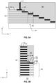
- FIGs. 3A-3D illustrates a detailed cross-sectional view of an exemplary conductor portion.
- FIGs. 3A-3D can also represent the cross-sectional views of staircase structure 202-1/202-2 along the same directions (as shown in FIG. 2B ), except that the bridge structure may have a different number of conductor/dielectric layer pairs along the z-direction.
- a staircase structure may include a staircase and a bridge structure in contact with the staircase.
- the staircase structure may include a staircase 306 and a bridge structure 308 (only a portion depicted in FIG. 3B ) in contact with staircase 306.
- the staircase structure may be formed over a substrate 302, similar to that in 3D memory device 100.
- An insulating structure 350 may be over at least staircase 306 such that at least staircase 306 is positioned in insulating structure 350.
- a word line VIA contact 316 may be formed in insulating structure 350 and landed on the landing area of a respective stair. For ease of illustration, only one word line VIA contact 316 is depicted.
- staircase 306 includes a plurality of stairs 314 extending along the x-direction, e.g., the word line direction. Each stair 314 may have a different depth along the z-direction. In some embodiments, except for the top stair, staircase 306 includes a conductor portion 320 at the top surface of at least one stair 314 and electrically and physically connected to a conductor layer 330 at the same level in bridge structure 308. In some embodiments, each stair 314 in staircase 306 may include a respective conductor portion 320. Conductor portion 320 may be in contact with a dielectric portion 324 (e.g., extending along the x-direction) of the same level.
- a dielectric portion 324 e.g., extending along the x-direction
- conductor portion 320 may be on and in contact with another dielectric portion, which is on and in contact with a dielectric layer 326 underneath. In some embodiments, in a respective stair 314, conductor portion 320 may be on and in contact with dielectric layer 326 without any other dielectric portion in between. In some embodiments, each dielectric layer 326 in staircase 306 is in contact with a dielectric layer 336 at the same level in bridge structure 308. In some embodiments, conductor portion 320 may be over more than one dielectric layer 336 in the respective stair 314.
- conductor portion 320 extends in the landing area of the respective stair 314.
- the non-overlapping portion (shown in FIG. 3D ) of conductor portion 320 may be cut off (e.g., not extending into) at the edge of an upper stair 314 (e.g., an immediately-above stair 314). That is, along the x-direction, little or no overlap is formed between the non-overlapping portions of adjacent conductor portions 320. In some embodiments, along the x-direction, no overlap is formed between the non-overlapping portion of any conductor portion 320.
- dielectric portion 324 and the other dielectric portion (if formed) may have the same material(s), which is different from the material(s) of dielectric layer 326.
- dielectric layer 326 includes silicon oxide.
- dielectric portion 324 includes silicon nitride.
- the other dielectric portion (if formed) has the same dimension along the x-direction as conductor portion 320.
- bottom surfaces of dielectric portion 324 and the other dielectric portion may be coplanar along the z-direction.
- a thickness of conductor portion 320 may be equal to or less than that of dielectric portion 324, and a thickness of the other dielectric portion (if formed) may be less than that of dielectric portion 324.
- a length D of conductor portion 320 may be equal to or less than the dimension of the respective stair 314.
- length D is equal to the dimension of the respective stair 314 along the y-direction.
- length D is less than the dimension of respective stair 314, and a second dielectric portion 323 is formed at the end of stair 314 away from bridge structure 308.
- Second dielectric portion 323 may have the same thickness as dielectric portion 324 along the z- direction, and may have the same material as dielectric portion 324.
- a width of second dielectric portion 323 may be less than, equal to, or greater than width d of conductor portion 320. Length D and width d of conductor portion 320 may each be sufficiently large to cover the landing area of the respective stair 314 and allow a respective word line VIA contact 316 to be formed at a desired location.
- the dielectric layers 326 may include the respective dielectric layer 326 in the same stair and one or more dielectric layers 326 in lower stairs 314.
- the dielectric portions 324 may include one or more dielectric portions 324 in lower stairs 314.
- the at least one conductor portion 320 is also over the other dielectric portion in the same stair 314.
- all the dielectric portions 324 and dielectric layers 326 underlying conductor portion 320 may be referred to as a dielectric structure 340, of which a thickness along the z-direction is equal to the distance between the bottom surface of the respective conductor portion 320 and the top surface of substrate 302.
- a length of dielectric structure 340, along the y-direction, is equal to that (e.g., length D) of conductor portion 320.
- a width of dielectric structure 340, along the x-direction is equal to that (e.g., width d) of conductor portion 320.
- dielectric structure 340 includes at least one pair of dielectric portion 324 and dielectric layer 326 corresponding to a lower stair 314 (e.g., stair 314 at a lower elevation/greater depth along the negative z-direction).
- each dielectric structure 340 includes at least one pair of dielectric portion 324 and dielectric layer 326 corresponding to a lower stair 314, and the dielectric layer 326 in the respective stair 314.
- FIG. 3C illustrates a lateral cross-sectional view of the staircase structure, showing the spatial relationships of a GLS 310, conductor layer 330, conductor portion 320, and dielectric portion 324.
- staircase 306 includes a connecting structure 321 in contact with bridge structure 308.
- Connecting structure 321, being a part of staircase 306 and extending along the x-direction, may include interleaved at least one conductor strip and at least one dielectric strip over substrate 302.
- a length L of connecting structure 321, along the y-direction is equal to or greater than zero.
- Each conductor strip may be in contact with conductor layer 330 and dielectric portion 324 of the same level, and each dielectric strip may be in contact with dielectric layer 336 and dielectric layer 326 of the same level.
- the material(s) of the conductor strip may be the same as that of conductor layer 330, and the material(s) of the dielectric strip may be the same as that of dielectric layer 336.
- the top conductor strip may also be in contact with the respective conductor portion 320, thus electrically connecting conductor portion 320 and conductor layer 330 of the same level.
- the thickness of each conductor strip may be the same as that of the respective conductor layer 330.
- conductor and dielectric strips, being a part of staircase 306, can be regarded as extensions of conductor layers 330 and dielectric layers 336 along the y-direction and into staircase 306.
- dielectric structure 340 is in contact with the respective connecting structure 321.
- the sum of d1 and d2 may be equal to D, if no connecting structure 321 is formed, and may be equal to (D-L), if connecting structure 321 is formed.
- d1 is desirably small such that it may be negligible compared to d2.
- d1 may be about 2% to about 20% (e.g., 2%, 3%, 5%, 8%, 10%, 15%, 18%, 20%) of d2.
- FIG. 3D illustrates a detailed structure of conductor portion 320.
- conductor portion 320 may be divided into a non-overlapping portion 320-1 and overlapping portions 320-2 and 320-3.
- Overlapping portion 320-2 may represent the portion of conductor portion 320 overlapping with the immediately-above stair (or the conductor portion 320 of the immediately-above stair) along the z-direction.
- Overlapping portion 320-3 may represent the portion of conductor portion 320 overlapping with the immediately-below stair (or the conductor portion 320 of the immediately-below stair) along the z-direction.
- overlapping portions 320-2 and 320-3 may have nominally the same shape and/or nominally the same dimensions.
- overlapping portion 320-2 has a right-triangle shape, in which the right angle is formed by the edge of the immediately-above stair 314 and the boundary of dielectric portion 324 along the x-direction.
- the lateral dimension of overlapping portion 320-2 may gradually decrease along the negative y-direction.
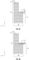
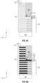
- FIGs. 4A-4D illustrate a fabrication process for forming an exemplary staircase structure of a 3D memory device, according to various embodiments of the present disclosure.
- FIGs. 5A and 5B illustrate a staircase before and after an ion implantation process, according to some embodiments.
- FIG. 6 is a flowchart of a method 600 for forming an exemplary staircase structure of a 3D memory device, according to some embodiments. It is understood that the operations shown in method 600 are not exhaustive and that other operations can be performed as well before, after, or between any of the illustrated operations. Further, some of the operations may be performed simultaneously, or in a different order than shown in FIG. 6 .
- method 600 starts at operation 602, in which a staircase structure having a staircase and a bridge structure is formed.
- FIG. 4A illustrates a corresponding structure.
- a staircase structure having a staircase 406 and a bridge structure 408 is formed over a substrate 402.
- Staircase 406 may be in contact with bridge structure 408.
- Staircase 406 may include interleaved a plurality of sacrificial layers 429 and a plurality of dielectric layers 426, forming a plurality of stairs 414 extending along the x-direction (e.g., referring to stairs 314 in FIG. 3A ).
- Each stair 414 may include at least one pair of sacrificial layer 429/dielectric layer 426.
- Bridge structure 408 may include interleaved a plurality of sacrificial layers 439 and a plurality of dielectric layers 436.
- each sacrificial layer 439 is in contact with a respective sacrificial layer 429 of the same level, and each dielectric layer 436 is in contact with a respective dielectric layer 436 of the same level.
- sacrificial layers 439 and 429 include the same material, such as silicon nitride.
- dielectric layers 436 and 426 include the same material, such as silicon oxide.
- a portion of the material stack may be patterned to form the stack structure.
- separate masks e.g., separate etching processes, can be used to form staircase 406 and bridge structure 408.
- the formation of staircase 406, in some embodiments, includes repetitive etching of the material stack using an etch mask (e.g., a patterned photoresist or PR layer) over the material stack.
- the etch mask can be repetitively trimmed inwardly and incrementally, often from all directions, to expose the portions of the material stack to be etched.
- the amount of trimmed PR can be directly related (e.g., determinant) to the dimensions of the stairs.
- the amount of trimmed PR along the x-direction may determine the width of stair 414 along the x-direction.
- the trimming of the PR layer can be obtained using a suitable etch, e.g., isotropic etch such as a wet etch.
- One or more PR layers can be formed and trimmed consecutively for the formation of the stairs.
- the etching of the material stack e.g., using a suitable etching process such as dry etch and/or wet etch, follows the trimming of the PR layer.
- the material stack is etched by a stair depth along the z-direction following each trimming of the PR layer.
- the stair depth may be equal to the number of dielectric material layer pairs (e.g., the number of first dielectric material layer/second dielectric material layer) included in a stair. In some embodiments, the number of dielectric material layer pairs is one.
- the trimming process of a photoresist mask, followed by the etching process of a material stack, is referred to herein as a trim-etch cycle.
- the number of trim-etch cycles can determine the number of stairs formed in the material along they-axis.
- the first dielectric material layers may form sacrificial layers 429, and the second dielectric material layers may form dielectric layers 426.
- Staircase 406 may be formed.
- each stair 414 includes a pair of sacrificial layer 429 and an underlying dielectric layer 426 (e.g., one sacrificial/dielectric pair).
- bridge structure 408 can be formed by patterning another portion of the material stack. An etch mask may or may not be used, depending on the design of bridge structure 408.
- bridge structure 408 may have the "wall-shape" structure as shown in FIG. 1B , or a staircase shape as shown in FIG. 2B .
- Bridge structure 408 may be formed with staircase 406 by the same etching process or by a different etching process.
- the formation of bridge structure 408 includes a photolithography process followed by a suitable etching process, such as dry etch and/or wet etch.
- the staircase structure, having staircase 406 and bridge structure 408, may be formed.
- sacrificial layer 429 is exposed at the top surface of the respective stair 414, after the formation of staircase 406.
- dielectric layer 426 may be under sacrificial layer 429.
- a protection layer 425 can be formed on the top surface of stair 414 to provide buffering and protection during the subsequent ion implantation process on stairs 414 such that the underlying sacrificial layer 429 can have the optimized physical properties. Protection layer 425 may cover at least the portion of stair 414 (i.e., sacrificial layer 429) that is to undergo the ion implantation process.
- protection layer 425 may cover at least the landing area (or possible landing area) of stair 414 (e.g., sacrificial layer 429). Protection layer 425 may include any suitable material with a suitable thickness along the z-direction, and may be formed with any suitable methods. In some embodiments, protection layer 425 includes a layer of dielectric material(s). In some embodiments, protection layer 425 includes a part of the second dielectric material layer (e.g., silicon oxide) that is not fully etched away during the formation of stairs 414. That is, at least a portion of second dielectric material layer immediately above the first dielectric material layer in staircase 406 may be retained during the etching of the material stack.
- the second dielectric material layer e.g., silicon oxide
- method 600 proceeds to operation 604, in which an ion implantation process is performed to form a sacrificial portion on the top surface of the respective stair.
- FIG. 4B illustrates a corresponding structure.
- an ion implantation process can be performed to form a sacrificial portion 419 on the top surface of at least one stair 414.
- a plurality of sacrificial portions 419 are formed, each on a respective stair 414.
- Sacrificial portion 419 may cover at least the landing area of the respective stair 414.
- sacrificial portion 419 covers the full width d (e.g., along the x-direction, referring back to FIG. 3A ) of the respective stair 414.
- Sacrificial portion 419 may be cut off at the edge of the immediately-above stair 414, such that sacrificial portion 419 does not extend under upper stair 414 along the x-direction.
- sacrificial portion 419 having a length D, may or may not cover the full length (e.g., along the y-direction, referring back to FIG. 3B ) of the respective stair 414.
- Sacrificial portion 419 may or may not be cut off at the boundary between bridge structure 408 and staircase 406, depending on the ion implantation process.
- a thickness of sacrificial portion 419 may be less than or equal to the thickness of sacrificial layer 429. In some embodiments, the thickness of sacrificial portion 419 is equal to the thickness of sacrificial layer 429.
- the ion implantation may change the physical properties of the treated portion of sacrificial layer 429 (i.e., sacrificial portion 419).
- sacrificial portion 419 may be bombarded by the ions to have higher porosity such that, in the subsequent gate-replacement process, an etchant to remove sacrificial layers 429 may have a higher etch rate on sacrificial portion 419 over sacrificial layers 429. That is, the etchant to remove sacrificial layers 429 may selectively etch sacrificial portion 419 over sacrificial layers 429.
- sacrificial portion 419 has a lower density than sacrificial layers 429, making it easier to be etched. In some embodiments, the ratio between the etch rate on sacrificial portion 419, and the etch rate on sacrificial layer 429 may be about 3: 1.
- the ion implantation process employs a tilted ion implantation process, at any suitable energy and with suitable ions. In some embodiments, the tilted ion implantation process may also implant ions into bridge structure 408. In some embodiments, the ions include boron (B) ions.
- thermal treatment such as an annealing process, can be performed after the ion implantation.
- sacrificial portion 419 may not fully cover stair 414 along the y- direction, and a second dielectric portion 423 may be formed from the portion of sacrificial layer 429 outside of the portion undergone the ion implantation process.
- a width of second dielectric portion 423 along the x-direction may be less than, equal to, or greater than that of the respective stair 414 (e.g., width d).
- a thickness of second dielectric portion 423 along the z-direction may be equal to or less than that of the respective sacrificial layer 429.
- FIG. 5B illustrates an enlarged view 502 of stairs 414 after the ion implantation process.
- sacrificial portion 419 may be formed in each stair 414, underlying a respective protection layer 425. Sacrificial portions 419 of adjacent stairs 414 may have no overlap along any direction.
- protection layer 425 may be removed after the ion implantation process to expose the underlying sacrificial portion 419.
- a suitable etching process e.g., dry etch and/or wet etch, is performed to remove protection layer 425.
- Dielectric layer 426 of each stair 414 may thus be cut off at the edge of the respective stair 414.
- protection layer 425 is retained.
- method 600 proceeds to operation 606, in which a plurality of lateral recesses are formed in the bridge structure, and a lateral recess portion is formed from each sacrificial portion.
- FIG. 4C illustrates a corresponding structure.
- a plurality of lateral recesses 428 may be formed in bridge structure 408, and a lateral recess portion 418 may be formed from a respective sacrificial portion 419.
- a GLS e.g., a slit structure, referred back to GLS 310 in FIG. 3C
- the GLS may extend in the staircase structure in the x-z plane, exposing substrate 402 and sacrificial/dielectric pairs (439/436) in bridge structure 408.
- lateral recess portion 418 is exposed on the top surface of respective stair 414. In some embodiments, if protection layer 425 is retained, lateral recess portion 418 is formed underlying the respective protection layer 425. In some embodiments, lateral recess portion 418 is in contact with second dielectric portion 423 laterally (along the negative y-direction). In some embodiments, lateral recess portion 418 is in contact with the underlying dielectric layer 426.
- the etchant has a higher etch rate on sacrificial portion 419 over sacrificial layers 439.
- the ratio of the etch rate on sacrificial portion 419 over sacrificial layers 439 may be in a range of about 5:1 to about 2:1. In some embodiments, the ratio is approximately 3:1. Because the etchant approaches staircase 406 from the GLS, a portion of the dielectric portion may be over etched as a result of the higher etch rate on sacrificial portion 419.
- the over-etched portion of the dielectric portion may overlap with the immediately-above stair 414 and corresponds to an overlapping portion (e.g., referring back to overlapping portion 320-2 in FIG.3D ) of the subsequently-formed conductor portion.
- the over-etched portion may be a part of lateral recess portion 418.
- the etch time is controlled such that at least a desired portion (e.g., a desired length along the y-direction) of the dielectric materials under each lateral recess portion 418 is retained.
- the retained dielectric materials under lateral recess portion 418 may form a respective dielectric structure under (e.g., referring back to FIG. 3A ) the landing area on which a respective word line VIA contact is to be formed.
- the etchant also removes a portion of each initial other dielectric portion, forming a respective other dielectric portion in contact and under lateral recess portion 418.
- an insulating structure 450 is formed over the staircase structure before the etching process such that at least staircase 406 is in insulating structure 450.
- Insulating structure 450 may include a suitable dielectric material and deposited by any suitable deposition method(s) such as CVD, ALD, and/or PVD.
- insulating structure 450 includes silicon oxide and is deposited by CVD.
- the dielectric material may be deposited to be in contact with sacrificial portion 419, forming insulating structure 450.
- the deposited dielectric material may accumulate on protection layer 425.
- Insulating structure 450 may then include protection layer 425 and any deposited dielectric material thereon. It should be noted that insulating structure 450 can be formed at any suitable time after the formation of staircase 406 and before the formation of the word line VIA contacts. The specific timing to form insulating structure 450 should not be limited by the embodiments of the present disclosure.
- a word line VIA contact 416 is formed in insulating structure 450 and in contact with the respective conductor portion 420.
- word line VIA contact 416 is formed on the non-overlapping portion of the respective conductor portion 420.
- Word line VIA contact 416 may be formed by patterning insulating structure 450 to form an opening that exposes conductor portion 420 and depositing a suitable conductive material to fill in the opening.
- the patterning of insulating structure 450 includes a photolithography process followed by a suitable etching process, e.g., dry etch and/or wet etch.
- the conductive material includes tungsten, cobalt, copper, aluminum, polysilicon, doped silicon, silicides, or any combination thereof.
- an ACS is formed in the GLS after conductor layers 430 and conductor portions 420 are formed.
- Embodiments of the present disclosure provide a 3D memory device.
- the 3D memory device includes a memory array structure and a staircase structure.
- the staircase structure is located in an intermediate of the memory array structure and divides the memory array structure into a first memory array structure and a second memory array structure along a lateral direction.
- the staircase structure includes a plurality of stairs extending along the lateral direction, and a bridge structure in contact with the first memory array structure and the second memory array structure.
- the plurality of stairs includes a stair above one or more dielectric pairs.
- the stair includes a conductor portion on a top surface of the stair and in contact with and electrically connected to the bridge structure, and a dielectric portion at a same level and in contact with the conductor portion.
- the stair is electrically connected to at least one of the first memory array structure and the second memory array structure through the bridge structure.
- a width of the conductor portion decreases.
- a portion of the conductor portion overlaps with an upper stair.
- a lateral dimension of the portion of the conductor portion decreases along the second lateral direction.
- the portion of the conductor portion has a lateral shape of a right triangle.
- the stair further includes a dielectric layer under the conductor portion and the dielectric portion.
- the conductor portion and the dielectric layer is each above the one or more dielectric pairs.
- a width of another portion of the conductor portion is equal to a dimension of the stair.
- a length of the conductor portion is equal to or less than a second dimension of the stair.
- a thickness of the conductor portion is equal to or less than a thickness of the dielectric portion along a vertical direction.
- the conductor portion includes at least one of tungsten, cobalt, copper, aluminum, silicides, and polysilicon.
- the dielectric portion includes silicon nitride. In some embodiments, the dielectric layer includes silicon oxide.
- the bridge structure includes interleaved a plurality of conductor layers each in contact with the first and second memory array structures.
- the conductor portion is in contact with and electrically connected to a respective conductor layer at the same level.
- each of the one or more dielectric pairs includes a dielectric portion and a dielectric layer corresponding to a lower stair.
- Embodiments of the present disclosure provide a 3D memory device.
- the 3D memory device includes a memory array structure and a landing structure in contact with the memory array structure.
- the landing structure includes a plurality of landing areas each at a respective depth extending along a lateral direction, and a bridge structure in contact with the memory array structure.
- the plurality of landing areas each includes a conductor portion on a respective top surface and a dielectric portion at a same level and in contact with the conductor portion.
- the conductor portion is electrically connected to the memory array structure through the bridge structure.
- a width of the conductor portion decreases along a second lateral direction perpendicular to the lateral direction and away from the bridge structure.
- the plurality of landing areas are each above one or more dielectric pairs.
- a portion of the conductor portion overlaps with an upper landing area.
- a lateral dimension of the portion of the conductor portion decreases along the second lateral direction.
- the portion of the conductor portion has a lateral shape of a right triangle.
- the plurality of landing areas further includes a dielectric layer under the conductor portion and the dielectric portion.
- the conductor portion and the dielectric layer is each above the one or more dielectric pairs.
- a width of another portion the conductor portion is equal to a dimension of the respective landing area.
- a length of the conductor portion is equal to or less than a second dimension of the respective landing area.
- the landing structure includes a plurality of stairs extending the lateral direction. In some embodiments, each of the plurality of landing areas is on the top surface of the respective stair.
- a thickness of the conductor portion is equal to or less than a thickness of the dielectric portion along a vertical direction.
- the conductor portion includes at least one of tungsten, cobalt, copper, aluminum, silicides, and polysilicon.
- the dielectric portion includes silicon nitride. In some embodiments, the dielectric layer includes silicon oxide.
- the bridge structure includes interleaved a plurality of conductor layers each in contact with the memory array structure.
- the conductor portion is in contact with and electrically connected to a respective one of the second conductors at the same level.
- each of the one or more dielectric pairs includes a dielectric portion and a dielectric layer corresponding to a lower landing area.
- Embodiments of the present disclosure provide a 3D memory device.
- the 3D memory device includes a memory array structure and a staircase structure.
- the staircase structure includes a plurality of stairs extending along a lateral direction.
- the plurality of stairs includes a stair having a conductor portion on a top surface of the stair and a dielectric portion at a same level and in contact with the conductor portion.
- the conduction portion is electrically connected to the memory array structure.
- a width of the conductor portion varies.
- a portion of the conductor portion overlaps with an upper stair.
- a lateral dimension of the portion of the conductor portion decreases along the second lateral direction.
- the portion of the conductor portion has a lateral shape of a right triangle.
- the staircase structure further includes a dielectric layer under the conductor portion and the dielectric portion.
- the conductor portion and the dielectric layer are each above the one or more dielectric pairs.
- a width of another portion of the conductor portion is equal to a dimension of the stair.
- a length of the conductor portion is equal to or less than a second dimension of the stair.
- a thickness of the conductor portion is equal to or less than a thickness of the dielectric portion along a vertical direction.
- the conductor portion includes at least one of tungsten, cobalt, copper, aluminum, silicides, and polysilicon.
- the dielectric portion includes silicon nitride. In some embodiments, the dielectric layer include silicon oxide.
- the 3D memory device further includes a bridge structure in contact with the staircase structure and the memory array structure.
- the bridge structure includes interleaved a plurality of conductor layers each in contact with the memory array structure.
- the conductor portion is in contact with and electrically connected to one of the conductor layers at the same level.
- the staircase structure is electrically connected to the memory array structure through the bridge structure.
- each of the one or more dielectric pairs includes a dielectric portion and a dielectric layer corresponding to a lower stair.
- Embodiments of the present disclosure provide a method for forming a staircase structure of a 3D memory device.
- the method includes the following operations. First, a plurality of stairs are formed having interleaved a plurality of first sacrificial layers and a plurality of first dielectric layers in a plurality of stairs.
- a bridge structure is formed in contact with the plurality of stairs, the bridge structure having interleaved a plurality of second sacrificial layers and a plurality of second dielectric layers.
- Each first sacrificial layer is in contact with a respective second sacrificial layer of the same level
- each first dielectric layer is in contact with a respective second dielectric layer of the same level.
- a sacrificial portion is formed in the first sacrificial layer corresponding to at least one of the stairs.
- the sacrificial portion is at a top surface of the respective stair and being cut off at an edge of an upper stair.
- the second sacrificial layers and the sacrificial portion are removed by a same etching process to respectively form a plurality of lateral recesses and a lateral recess portion.
- a plurality of conductor layers are formed in the lateral recesses and a conductor portion is formed in the lateral recess portion and in contact with a respective one of the conductor layers.
- the method further includes forming a dielectric portion in the respective first sacrificial layer.
- the sacrificial portion is in contact and at a same level with the sacrificial portion.
- an etch rate on the sacrificial portion is higher than an etch rate on the second sacrificial layers.
- a ratio of etch rate on the sacrificial portion over the etch rate on the second sacrificial layers is approximately 3:1.
- forming the lateral recess portion further includes removing, by the etching process, a portion of the dielectric portion under the upper stair.
- forming the sacrificial portion includes performing an ion implantation process on an exposed portion of the first sacrificial layer of the at least one of the stairs to alter an etch rate of the exposed portion of the first sacrificial layer in the etching process.
- the ion implantation process includes a tilted ion implantation process with boron (B).
- the method further includes forming a protection layer on the first sacrificial layer before the ion implantation process.
- the method further includes removing the protection layer after the ion implantation process.
- the method further includes retaining a portion of the first sacrificial layers and first dielectric layers corresponding to a lower stair under the sacrificial portion.
- the method further includes removing, by the etching process, another portion of the first sacrificial layers and the first dielectric layers under the sacrificial portion.
- the method further includes forming a slit structure in the staircase structure and removing the plurality of second sacrificial layers and the sacrificial portion through the slit structure.
- forming the plurality of conductor and the conductor portion includes depositing a conductor material to fill in the lateral recesses and the lateral recess portion.
- the method further includes forming a contact on the conductor portion.
Landscapes
- Semiconductor Memories (AREA)
- Non-Volatile Memory (AREA)
- Physics & Mathematics (AREA)
- Engineering & Computer Science (AREA)
- Plasma & Fusion (AREA)
- Internal Circuitry In Semiconductor Integrated Circuit Devices (AREA)
Abstract
Description
- Embodiments of the present disclosure relate to three-dimensional (3D) memory devices and fabrication methods thereof.
- Planar memory cells are scaled to smaller sizes by improving process technology, circuit design, programming algorithm, and fabrication process. However, as feature sizes of the memory cells approach a lower limit, planar process and fabrication techniques become challenging and costly. As a result, memory density for planar memory cells approaches an upper limit.
- A 3D memory architecture can address the density limitation in planar memory cells. The 3D memory architecture includes a memory array and peripheral devices for controlling signals to and from the memory array.
- Embodiments of 3D memory devices having staircase structures and methods for forming the same are disclosed herein.
- In one example, the 3D memory device includes a memory array structure and a staircase structure. The staircase structure is located in an intermediate of the memory array structure and divides the memory array structure into a first memory array structure and a second memory array structure along a lateral direction. The staircase structure includes a plurality of stairs extending along the lateral direction, and a bridge structure in contact with the first memory array structure and the second memory array structure. The plurality of stairs includes a stair above one or more dielectric pairs. The stair includes a conductor portion on a top surface of the stair and in contact with and electrically connected to the bridge structure, and a dielectric portion at a same level and in contact with the conductor portion. The stair is electrically connected to at least one of the first memory array structure and the second memory array structure through the bridge structure. Along a second lateral direction perpendicular to the lateral direction and away from the bridge structure, a width of the conductor portion decreases.
- In another example, the 3D memory device includes a memory array structure and a landing structure in contact with the memory array structure. The landing structure includes a plurality of landing areas each at a respective depth extending along a lateral direction, and a bridge structure in contact with the memory array structure. The plurality of landing areas each includes a conductor portion on a respective top surface and a dielectric portion at a same level and in contact with the conductor portion. The conductor portion is electrically connected to the memory array structure through the bridge structure. A width of the conductor portion decreases along a second lateral direction perpendicular to the lateral direction and away from the bridge structure. The plurality of landing areas are each above one or more dielectric pairs.
- In still another example, the 3D memory device includes a memory array structure and a staircase structure. The staircase structure includes a plurality of stairs extending along a lateral direction. The plurality of stairs includes a stair having a conductor portion on a top surface of the stair and a dielectric portion at a same level and in contact with the conductor portion. The conduction portion is electrically connected to the memory array structure. Along a second lateral direction perpendicular to the lateral direction, a width of the conductor portion varies.
- In still another example, a method for forming a staircase structure of 3D memory device includes the following operations. First, a plurality of stairs are formed having interleaved a plurality of first sacrificial layers and a plurality of first dielectric layers in a plurality of stairs. A bridge structure is formed in contact with the plurality of stairs, the bridge structure having interleaved a plurality of second sacrificial layers and a plurality of second dielectric layers. Each first sacrificial layer is in contact with a respective second sacrificial layer of the same level, and each first dielectric layer is in contact with a respective second dielectric layer of the same level. A sacrificial portion is formed in the first sacrificial layer corresponding to at least one of the stairs. The sacrificial portion is at a top surface of the respective stair and being cut off at an edge of an upper stair. The second sacrificial layers and the sacrificial portion are removed by a same etching process to respectively form a plurality of lateral recesses and a lateral recess portion. A plurality of conductor layers are formed in the lateral recesses and a conductor portion is formed in the lateral recess portion and in contact with a respective one of the conductor layers.
- The accompanying drawings, which are incorporated herein and form a part of the specification, illustrate embodiments of the present disclosure and, together with the description, further serve to explain the principles of the present disclosure and to enable a person skilled in the pertinent art to make and use the present disclosure.
-
FIG. 1A illustrates a schematic diagram of an exemplary 3D memory device having staircase structures, according to some embodiments of the present disclosure. -
FIG. 1B illustrates a top front perspective view of an exemplary staircase structure of a 3D memory device shown inFIG. 1A , according to some embodiments of the present disclosure. -
FIG. 1C illustrates a plan view of an exemplary 3D memory device shown inFIG. 1A , according to some embodiments of the present disclosure. -
FIG 1D illustrates another plan view of an exemplary 3D memory device shown inFIG. 1A , according to some embodiments of the present disclosure. -
FIG. 1E illustrates a detailed top front perspective view of an exemplary staircase structure of a 3D memory device shown inFIG. 1A , according to some embodiments of the present disclosure. -
FIG. 2A illustrates a schematic diagram of another exemplary 3D memory device having staircase structures, according to some embodiments of the present disclosure. -
FIG. 2B illustrates a top front perspective view of an exemplary staircase structure of a 3D memory device shown inFIG. 2A , according to some embodiments of the present disclosure. -
FIG. 2C illustrates a plan view of an exemplary 3D memory device shown inFIG. 2A , according to some embodiments of the present disclosure. -
FIG. 3A illustrates a cross-sectional view of an exemplary 3D memory device having a staircase structure, according to some embodiments of the present disclosure. -
FIG. 3B illustrates another cross-sectional view of the 3D memory device shown inFIG. 3A , according to some embodiments of the present disclosure. -
FIG. 3C illustrates another cross-sectional view of the 3D memory device shown inFIG. 3A , according to some embodiments of the present disclosure. -
FIG. 3D illustrates a detailed cross-section view of a conductor portion shown inFIG. 3C , according to some embodiments of the present disclosure. -
FIGs. 4A - 4E illustrate a fabrication process for forming an exemplary staircase structure of a 3D memory device, according to some embodiments of the present disclosure. -
FIGs. 5A and 5B illustrate an exemplary staircase before and after an ion implantation process, according to some embodiments. -
FIG. 6 is a flowchart of a method for forming an exemplary staircase structure of a 3D memory device, according to some embodiments. - Embodiments of the present disclosure will be described with reference to the accompanying drawings.
- Although specific configurations and arrangements are discussed, it should be understood that this is done for illustrative purposes only. A person skilled in the pertinent art will recognize that other configurations and arrangements can be used without departing from the spirit and scope of the present disclosure. It will be apparent to a person skilled in the pertinent art that the present disclosure can also be employed in a variety of other applications.
- It is noted that references in the specification to "one embodiment," "an embodiment," "an example embodiment," "some embodiments," etc., indicate that the embodiment described may include a particular feature, structure, or characteristic, but every embodiment may not necessarily include the particular feature, structure, or characteristic. Moreover, such phrases do not necessarily refer to the same embodiment. Further, when a particular feature, structure or characteristic is described in connection with an embodiment, it would be within the knowledge of a person skilled in the pertinent art to effect such feature, structure or characteristic in connection with other embodiments whether or not explicitly described.
- In general, terminology may be understood at least in part from usage in context. For example, the term "one or more" as used herein, depending at least in part upon context, may be used to describe any feature, structure, or characteristic in a singular sense or may be used to describe combinations of features, structures or characteristics in a plural sense. Similarly, terms, such as "a," "an," or "the," again, may be understood to convey a singular usage or to convey a plural usage, depending at least in part upon context. In addition, the term "based on" may be understood as not necessarily intended to convey an exclusive set of factors and may, instead, allow for existence of additional factors not necessarily expressly described, again, depending at least in part on context.
- It should be readily understood that the meaning of "on," "above," and "over" in the present disclosure should be interpreted in the broadest manner such that "on" not only means "directly on" something but also includes the meaning of "on" something with an intermediate feature or a layer therebetween, and that "above" or "over" not only means the meaning of "above" or "over" something but can also include the meaning it is "above" or "over" something with no intermediate feature or layer therebetween (i.e., directly on something).
- Further, spatially relative terms, such as "beneath," "below," "lower," "above," "upper," and the like, may be used herein for ease of description to describe one element or feature's relationship to another element(s) or feature(s) as illustrated in the figures. The spatially relative terms are intended to encompass different orientations of the device in use or operation in addition to the orientation depicted in the figures. The apparatus may be otherwise oriented (rotated 90 degrees or at other orientations), and the spatially relative descriptors used herein may likewise be interpreted accordingly.
- As used herein, the term "substrate" refers to a material onto which subsequent material layers are added. The substrate itself can be patterned. Materials added on top of the substrate can be patterned or can remain unpatterned. Furthermore, the substrate can include a wide array of semiconductor materials, such as silicon, germanium, gallium arsenide, indium phosphide, etc. Alternatively, the substrate can be made from an electrically non-conductive material, such as a glass, a plastic, or a sapphire wafer.
- As used herein, the term "layer" refers to a material portion including a region with a thickness. A layer can extend over the entirety of an underlying or overlying structure or may have an extent less than the extent of an underlying or overlying structure. Further, a layer can be a region of a homogeneous or inhomogeneous continuous structure that has a thickness less than the thickness of the continuous structure. For example, a layer can be located between any pair of horizontal planes between, or at, a top surface and a bottom surface of the continuous structure. A layer can extend laterally, vertically, and/or along a tapered surface. A substrate can be a layer, can include one or more layers therein, and/or can have one or more layer thereupon, thereabove, and/or therebelow. A layer can include multiple layers. For example, an interconnect layer can include one or more conductor and contact layers (in which interconnect lines and/or vertical interconnect access (VIA) contacts are formed) and one or more dielectric layers.
- As used herein, the term "nominal/nominally" refers to a desired, or target, value of a characteristic or parameter for a component or a process operation, set during the design phase of a product or a process, together with a range of values above and/or below the desired value. The range of values can be due to slight variations in manufacturing processes or tolerances. As used herein, the term "about" indicates the value of a given quantity that can vary based on a particular technology node associated with the subject semiconductor device. Based on the particular technology node, the term "about" can indicate a value of a given quantity that varies within, for example, 10-30% of the value (e.g., ±10%, ±20%, or ±30% of the value).
- As used herein, the term "3D memory device" refers to a semiconductor device with vertically oriented strings of memory cell transistors (referred to herein as "memory strings," such as NAND memory strings) on a laterally-oriented substrate so that the memory strings extend in the vertical direction with respect to the substrate. As used herein, the term "vertical/vertically" means nominally perpendicular to the lateral surface of a substrate.
- In some 3D memory devices, memory cells for storing data are vertically stacked through a stacked storage structure (e.g., a memory stack). 3D memory devices usually include staircase structures formed in the vicinity of the stacked storage structure for purposes such as word line fan-out. As the demand for higher storage capacity continues to increase, the number of vertical levels of the stacked storage structure also increases, and it has become more difficult to form the word line VIA contacts on the stairs without punching through the contacts and causing short circuits. For example, the word line VIA contacts are often formed by forming openings in contact with the stairs (e.g., the landing area of the stairs) in an insulating structure in which the staircase structure is placed, and filling the openings with a conductive material. Conventionally, these openings, formed to be in contact with stairs at different depths/heights, are formed in the same etching process. Because of the variation in opening depths, the openings are often not etched evenly or desirably. For example, the openings in contact with lower stairs (e.g., the deeper openings) and the openings in contact with higher stairs (e.g., the shallower openings) undergo the same etching time, resulting the openings in contact with the higher stairs to be over etched. The over-etching can cause the conductor layers (e.g., word lines) on the top surfaces of the higher stairs to be undesirably damaged or even etched through. The word line VIA contacts can undesirably be in contact with other conductor layers underlying the respective conductor layers, causing a punch-through that leads to short circuits or undesirable leakage. To solve this issue, efforts, such as thickening the conductor layer for landing, have been made. However, a thicker landing area still cannot desirably reduce the possibility of punch-through, and the fabrication process becomes more challenging.
- Various embodiments in accordance with the present disclosure provide staircase structures and fabrication methods thereof. A staircase structure, having a plurality of stairs, can include a conductor portion at the top surface of at least one stair and a dielectric structure, including one or more dielectric pairs, under the conductor portion. The conductor portion covers at least the landing area of the respective stair (e.g., a portion of the stair) such that a word line VIA contact can be in contact with and electrically connected to the respective stair. The thickness of the dielectric structure can be equal to the distance from the bottom surface of the conductor portion to the top surface of the substrate and is desirably thick to prevent interference between conductor portions at different stairs due to punch-through. Along the lateral direction that is perpendicular to the direction the stairs extend, a width of each conductor portion may decrease gradually from an end.
- In embodiments of the present disclosure, the conductor portion includes an overlapping portion and a non-overlapping portion. The overlapping portions refer to the portions of the conductor portion that overlap with an immediately-above and/or an immediately-below stair (or the conductor portion of the immediately-above/immediately-below stair). The non-overlapping portion refers to the portion of the conductor portion not overlapping with an upper or a lower stair. A word line VIA contact can be formed on the non-overlapping portion of the conductor portion. The non-overlapping portion of the conductor portion can have a desirably large landing area for the respective word line VIA contact to be formed on. In some embodiments, along the direction the stairs extend, the dimension of the non-overlapping portion of the conductor portion becomes nominally the same as the dimension of the stair.
- In some embodiments, over the dielectric structure under the conductor portion includes a respective dielectric layer and one or more underlying dielectric pairs, each including a dielectric portion and a dielectric layer in a lower stair. In some embodiments, the number of dielectric pairs under the conductor portion of a respective stair is equal to the number of stairs/levels under the stair. Even if a punch-through occurs on any conductor portion, the word line VIA contact has no contact on the conductor portion (or word line) of any lower stairs, and leakage or short circuits can be reduced/eliminated. It might then be less difficult to form the openings.
- In various embodiments, the stairs are formed in a staircase structure that is located at the intermediate of memory array structures or on the side of a memory array structure. The staircase structure can include a bridge structure that has interleaved a plurality of conductor layers and dielectric layers. The conductor layers are conductively connected to the memory cells in the memory array structure(s). The conductor portions of each stair can be in contact with a conductor layer at the same level along a direction perpendicular to the direction the stairs extend such that voltages can be applied to the memory cells through the conductor portions and the conductor layers at the same levels.
- To form the conductor portion, an ion implantation process is performed before the gate-replacement. The ion implantation process is employed to form a sacrificial portion, which is an ion-implantation-treated portion of the respective sacrificial layer at the top surface of the stair. The ion implantation process can alter the physical properties of the treated portion such that the sacrificial portion can be etched at a higher rate than other parts of the sacrificial layer that are not treated with the ion implantation. One etching process can then be applied to remove the sacrificial layers (e.g., for forming word lines in the bridge structure) and the sacrificial portions simultaneously, such that lateral recesses and lateral recess portions can be formed. The dielectric structure under the sacrificial portion can be retained. In some embodiments, the lateral recess portion includes an over-etched portion of the sacrificial layer under the immediately-above stair due to the higher etch rate on the sacrificial portion. A conductor material is deposited to fill the lateral recess portion at each stair and lateral recesses in the bridge structure. A plurality of conductor layers can be formed in the bridge structure. A plurality of conductor portions, each at a respective stair and over a respective dielectric structure, can be formed in the staircase. In some embodiments, the over-etched portion, after being filled with the conductor portion, forms the overlapping portion between adjacent conductor portions.
-
FIGs. 1A-1C andFIGs. 2A-2C illustrate schematic views of3D memory devices FIGs. 1A-1C illustrate a layout in which the staircase structure is located at the intermediate of a memory plane, andFIGs. 2A-2C illustrate a layout in which the staircases are located on the two sides of a memory plane. The staircase structure of the present disclosure can be formed in both3D memory devices 3D memory device 100. In some embodiments, the staircase structures in3D memory device 200 may be formed in a similar fabrication process. It is noted that x and y axes are included inFIGs. 1A and2A to illustrate two orthogonal (perpendicular) directions in the wafer plane. The x-direction is the word line direction of the respective 3D memory device, and the y-direction is the bit line direction of the respective 3D memory device. It should be noted that the structures in the present disclosure are merely for illustration purposes only and thus, do not indicate the dimensions, ratios, or shapes in actual products. -
FIG. 1A illustrates a schematic diagram of an exemplary3D memory device 100 having astaircase structure 102, according to some embodiments of the present disclosure. In some embodiments,3D memory device 100 includes multiple memory planes. A memory plane can include a first memory array structure 104-1, a second memory array structure 104-2, and astaircase structure 102 in the intermediate of first and second memory array structures 104-1 and 104-2. First and second memory array structures 104-1 and 104-2, together regarded as a memory array structure, may or may not have the same area. In some embodiments,staircase structure 102 is in the middle of first and second memory array structures 104-1 and 104-2. For example, first and second memory array structures 104-1 and 104-2 may be symmetric in the x-direction with respect tostaircase structure 102. It is understood that in some examples,staircase structure 102 may be in the intermediate, but not in the middle (center), of first and second memory array structures 104-1/104-2, such that first and second memory array structures 104-1 and 104-2 may have different sizes and/or numbers of memory cells. In some embodiments,3D memory device 100 is a NAND Flash memory device in which memory cells are provided in the form of an array of NAND memory strings (not shown inFIG. 1A ) in first and second memory array structures 104-1 and 104-2. First and second memory array structures 104-1 and 104-2 can include any other suitable components including, but not limited to, gate line slits (GLSs), through array contacts (TACs), array common sources (ACSs), etc. - Each word line (not shown in
FIG. 1A ) of the memory plane extending laterally in the x-direction can be separated bystaircase structure 102 into two parts: a first word line part across first memory array structure 104-1, and a second word line part across second memory array structure 104-2. The two parts of each word line can be electrically connected by a bridge structure (shown asbridge structure 108 instaircase structure 102 inFIGs. 1B and1C ) at a respective stair instaircase structure 102. A row decoder (not shown) can be formed right above, below, or in proximity torespective staircase structure 102. Each row decoder can bilaterally drive word lines in opposite directions from the intermediate of the memory plane. - The detailed structure of
staircase structure 102 is illustrated inFIGs. 1B and1C .FIG. 1B illustrates a top front view ofstaircase structure 102 in3D memory device 100.FIG. 1C illustrates a top view ofstaircase structure 102 and its spatial relationship with adjacent first and second memory array structures 104-1 and 104-2. For ease of illustration,FIG. 1C only depicts onestaircase structure 102. In various embodiments,3D memory device 100 includes a plurality of staircase structures between first and second memory array structures 104-1 and 104-2, e.g., aligned withstaircase structure 102 along the y-direction. For example, another staircase structure may be the same asstaircase structure 102 andmirror staircase structure 102 along the y-direction. Also, other possible structures such as dummy staircases are omitted instaircase structure 102 for ease of illustration. -
FIG. 1B depictsstaircase structure 102 having astaircase 106 and abridge structure 108, in contact with each other.FIG. 1E illustrates a detailed 3D perspective view ofstaircase structure 102.Staircase structure 102 may be on a substrate 10 (shown inFIG. 1D ), which can include silicon (e.g., single crystalline silicon), silicon germanium (SiGe), gallium arsenide (GaAs), germanium (Ge), silicon on insulator (SOI), or any other suitable materials. -
Staircase 106 may include a plurality ofstairs 114 extending along the word line direction, e.g., the x-direction. Eachstair 114 may have a different depth along the z-direction and a landing area, e.g., for forming contact with a corresponding word line VIA contact. Each stair 114 (as shown as a "level") ofstaircase 106 can include one or more material layer pairs. In some embodiments, the top material layer of eachstair 114 includes a conductor portion for interconnection with a word line VIA contact in the vertical direction. In some embodiments, every twoadjacent stairs 114 ofstaircase 106 are offset by a nominally same distance in the z-direction and a nominally same distance in the x-direction. Each offset thus can form a "landing area" for interconnection with word line contacts of the 3D memory device in the z-direction direction. In some embodiments, eachstair 114 includes at least one dielectric layer under the conductor portion. -
Bridge structure 108 can include vertically interleaved conductor layers and dielectric layers (not shown), and the conductor layers (e.g., metal layers or polysilicon layers) can function as part of word lines. Different fromstaircase 106 in which the word lines therein are cut off from the memory array structure (e.g., 104-1 and/or 104-2) in the x-direction (e.g., in the positive x-direction, the negative x-direction, or both), the word lines inbridge structure 108 can be preserved to bridge the word line VIA contacts landed onstairs 114 and the memory array structures (e.g., 104-1 and/or 104-2) in order to achieve the bilateral word line-driving scheme. In some embodiments, at least onestair 114 in a staircase instaircase 106 is electrically connected to at least one of the first memory array structure 104-1 and the second memory array structure 104-2 throughbridge structure 108. At least one word line can extend laterally in the memory array structure (e.g., 104-1 and/or 104-2) andbridge structure 108, such that the at least onestair 114 can be electrically connected to the at least one of the first and second memory array structures (e.g., 104-1 and/or 104-2) throughbridge structure 108 by the at least one word line. In one example, astair 114 instaircase 106 may be electrically connected to first memory array structure 104-1 (in the negative x-direction) by a respective word line part extending in the negative x-direction throughbridge structure 108. In some embodiments, the at least onestair 114 instaircase 106 is electrically connected to each of first memory array structure 104-1 and second memory array structure 104-2 throughbridge structure 108, e.g., by the respective word line parts extending in the negative and positive x-directions, respectively. - The conductor portion in
staircase 106 and conductive layers inbridge structure 108 can each include conductive materials including, but not limited to, tungsten (W), cobalt (Co), copper (Cu), aluminum (Al), polycrystalline silicon (polysilicon), doped silicon, silicides, or any combination thereof. The dielectric layers instaircase 106 andbridge structure 108 can include dielectric materials including, but not limited to, silicon oxide, silicon nitride, silicon oxynitride, or any combination thereof. In some embodiments, the conductor portions and conductor layers include the same material, e.g., metals, such as tungsten, and the dielectric layers include the same material, such as silicon oxide. -
FIGs. 1C and1D illustratestaircase structure 102 between first and second memory array structures 104-1 and 104-2. As shown inFIGs. 1C and1D ,staircase 106 may include a plurality ofstairs 114 extending along the x-direction, and a wordline VIA contact 116 is formed on at least one (e.g., each)stair 114. Each of first and second memory array structures 104-1 and 104-2 may include one or more memory blocks, and each memory block includes one ormore memory fingers 120. In some embodiments,staircase structure 102 may be between a pair ofmemory fingers 120 along the y-direction. Eachmemory finger 120 may include a plurality ofmemory strings 112 extending along the z-direction.Memory string 112 may include a channel structure that has a blocking layer, a memory layer, a tunneling layer, a semiconductor layer, and optionally, a dielectric core in a channel hole and arranged radially from the sidewall towards the center of the channel hole. Memory strings 112 may intersect with a plurality of word lines (e.g., conductor layers in memory fingers 120), forming a plurality of memory cells. The memory cells may form a memory cell array in the respective memory array structure. In some embodiments,GLSs 110, extending along the x-direction and the z-direction, divides memory cells in first and second memory array structures 104-1 and 104-2 into a plurality ofmemory fingers 120 along the y-direction. - To achieve the bilateral word line-driving scheme,
bridge structure 108 connects (both physically and electrically) first memory array structure 104-1 and/or second memory array structure 104-2, according to some embodiments. That is,staircase structure 102 does not completely cut off the memory array structure in the intermediate, but instead leaves the first and second memory array structures 104-1 and 104-2 connected bybridge structure 108 thereof, according to some embodiments. Each word line thus can be bilaterally driven (in both positive and negative x-directions) from a respective wordline VIA contact 116 in the intermediate of3D memory device 100 throughbridge structures 108.FIGs. 1C and1D illustrate exemplary current paths of the bilateral word line-driving scheme withstaircase structures 102. Current paths indicated by the arrows represent currents passing through separate word lines at different levels, respectively. -
FIGs. 2A-2C illustrates a schematic diagram of a3D memory device 200 having staircase structures 202-1 and 202-2 each on a respective side of amemory array structure 204. Staircase structures 202-1 and 202-2, andmemory array structure 204 may be on asubstrate 101, similar to that in3D memory device 100.3D memory device 200 may include a memory plane that has a memory cell array in amemory array structure 204. Different from3D memory device 100,3D memory device 200 includes two staircase structures 202-1 and 202-2 at opposite sides in the x-direction ofmemory array structure 204. Each word line of the memory plane extends laterally in the x-direction across the entire memory plane to a respective stair (level) in staircase structure 202-1 or 202-2. A row decoder (not shown) is formed right above, below, or in proximity to the respective staircase structure. That is, each row decoder unilaterally (either in the positive or negative x-direction, but not both) drives one-half of the memory cells through one-half of the word lines, each of which crosses the entire memory plane. - Staircase structure 202-1 and 202-2 may have similar/same structures.
FIG. 2B illustrates a front top view of a staircase structure that can represent each of staircase structures 202-1 and 202-2. The staircase structure may include astaircase 206 that has a plurality ofstairs 214 extending along the x-direction, similar tostaircase 106. The staircase structure also includes abridge structure 208 electrically and physically connected tostaircase 206.Bridge structure 208 may include interleaved conductor layers and dielectric layers, similar to thatbridge structure 108. In some embodiments,bridge structure 208 includes a plurality of stairs extending along the x-direction, each of the stairs corresponding to a respective stair ofstaircase 206.Staircase 206 may be similar tostaircase 106, e.g., at least onestair 214 includes a conductor portion at the top surface and electrically connected to a conductor layer at the same level inbridge structure 208. Conductor layers inbridge structure 208 may be word line parts that are electrically connected to word lines (e.g., conductor layers) inmemory array structure 204. -
FIG. 2C illustrates staircase structures 202-1 and 202-2 each on a respective side ofmemory array structure 204. As shown inFIG. 2C ,staircase 206 may include a plurality ofstairs 214 extending along the x-direction, and a wordline VIA contact 216 is formed on at least one (e.g., each)stair 214.Memory array structures 204 may include one or more memory blocks, and each memory block includes one ormore memory fingers 220. Eachmemory finger 220 may include a plurality ofmemory strings 212, similar tomemory strings 112 in3D memory device 200. Memory strings 212 may intersect with a plurality of word lines (e.g., conductor layers in memory fingers 220), forming a plurality of memory cells, which form a memory cell array in the respective memory array structure. In some embodiments,GLSs 210, extending along the x-direction and the z-direction, divides memory cells inmemory array structure 204 into a plurality ofmemory fingers 220 along the y-direction. - To achieve the unilateral word line-driving scheme,
bridge structures 208 each connects (both physically and electrically)memory array structure 204, according to some embodiments. Each word line thus can be unilaterally driven (in positive or negative x-direction) from a respective wordline VIA contact 216 on one side of3D memory device 200 throughbridge structures 208. As shown inFIG. 2C , current paths indicated by the arrows represent currents passing through two separate word lines at different levels, respectively. -
FIGs. 3A-3D illustrates three cross-sectional views of a staircase structure (e.g., 102), each being orthogonal of one another. Specifically,FIGs. 3A and 3B respectively depict cross-sectional views ofstaircase structure 102 along the A-A' and the B-B' directions, as shown inFIG. 1B .FIG. 3A illustrates the cross-sectional view of thestaircase 106, which shows the non-overlapping portions of the conductor portions. As shown inFIG. 1B , A-A' direction represents the x-z plane, and B-B' direction represents the z-y plane.FIG. 3C illustrates the x-y cross-sectional view of a stair/level ofstaircase structure 102.FIG. 3D illustrates a detailed cross-sectional view of an exemplary conductor portion.FIGs. 3A-3D can also represent the cross-sectional views of staircase structure 202-1/202-2 along the same directions (as shown inFIG. 2B ), except that the bridge structure may have a different number of conductor/dielectric layer pairs along the z-direction. - As previously described, in a 3D memory device, a staircase structure may include a staircase and a bridge structure in contact with the staircase. As shown in
FIGs. 3A and 3B , the staircase structure may include astaircase 306 and a bridge structure 308 (only a portion depicted inFIG. 3B ) in contact withstaircase 306. The staircase structure may be formed over asubstrate 302, similar to that in3D memory device 100. An insulatingstructure 350 may be over atleast staircase 306 such that atleast staircase 306 is positioned in insulatingstructure 350. A wordline VIA contact 316 may be formed in insulatingstructure 350 and landed on the landing area of a respective stair. For ease of illustration, only one wordline VIA contact 316 is depicted. Insulatingstructure 350 may include any suitable dielectric material such as silicon oxide, silicon nitride, and/or silicon oxynitride. Wordline VIA contact 316 may include tungsten, cobalt, copper, aluminum, polysilicon, doped silicon, silicides, or any combination thereof.Bridge structure 308 may include interleaved a plurality of conductor layers 330 and dielectric layers 336, similar to those in3D memory device 100. - As shown in
FIGs. 3A and 3B ,staircase 306 includes a plurality ofstairs 314 extending along the x-direction, e.g., the word line direction. Eachstair 314 may have a different depth along the z-direction. In some embodiments, except for the top stair,staircase 306 includes aconductor portion 320 at the top surface of at least onestair 314 and electrically and physically connected to aconductor layer 330 at the same level inbridge structure 308. In some embodiments, eachstair 314 instaircase 306 may include arespective conductor portion 320.Conductor portion 320 may be in contact with a dielectric portion 324 (e.g., extending along the x-direction) of the same level. Optionally, in arespective stair 314,conductor portion 320 may be on and in contact with another dielectric portion, which is on and in contact with adielectric layer 326 underneath. In some embodiments, in arespective stair 314,conductor portion 320 may be on and in contact withdielectric layer 326 without any other dielectric portion in between. In some embodiments, eachdielectric layer 326 instaircase 306 is in contact with a dielectric layer 336 at the same level inbridge structure 308. In some embodiments,conductor portion 320 may be over more than one dielectric layer 336 in therespective stair 314. - As shown in
FIG. 3A , along the x-direction,conductor portion 320 extends in the landing area of therespective stair 314. The non-overlapping portion (shown inFIG. 3D ) ofconductor portion 320 may be cut off (e.g., not extending into) at the edge of an upper stair 314 (e.g., an immediately-above stair 314). That is, along the x-direction, little or no overlap is formed between the non-overlapping portions ofadjacent conductor portions 320. In some embodiments, along the x-direction, no overlap is formed between the non-overlapping portion of anyconductor portion 320. In some embodiments, along the x-direction, a width d of the non-overlapping portion ofconductor portion 320 may be equal to or less than the dimension ofstair 314. A respective word line VIA contact may be formed on the non-overlapping portion ofconductor portion 320. - In some embodiments, in
stair 314,dielectric portion 324 and the other dielectric portion (if formed) may have the same material(s), which is different from the material(s) ofdielectric layer 326. In some embodiments,dielectric layer 326 includes silicon oxide. In some embodiments,dielectric portion 324 includes silicon nitride. In some embodiments, the other dielectric portion (if formed) has the same dimension along the x-direction asconductor portion 320. Instair 314, bottom surfaces ofdielectric portion 324 and the other dielectric portion may be coplanar along the z-direction. Along the z-direction, a thickness ofconductor portion 320 may be equal to or less than that ofdielectric portion 324, and a thickness of the other dielectric portion (if formed) may be less than that ofdielectric portion 324. - As shown in
FIG. 3B , along the y-direction, a length D ofconductor portion 320 may be equal to or less than the dimension of therespective stair 314. In some embodiments, length D is equal to the dimension of therespective stair 314 along the y-direction. In some embodiments, length D is less than the dimension ofrespective stair 314, and a seconddielectric portion 323 is formed at the end ofstair 314 away frombridge structure 308.Second dielectric portion 323 may have the same thickness asdielectric portion 324 along the z-direction, and may have the same material asdielectric portion 324. Along the x-direction, a width of seconddielectric portion 323 may be less than, equal to, or greater than width d ofconductor portion 320. Length D and width d ofconductor portion 320 may each be sufficiently large to cover the landing area of therespective stair 314 and allow a respective wordline VIA contact 316 to be formed at a desired location. - As shown in
FIGs. 3A and 3B ,conductor portion 320 may be over at least arespective dielectric layer 326 in thesame stair 314. In some embodiments, in eachstair 314,conductor portion 320 is in contact with and on therespective dielectric layer 326. Meanwhile,dielectric portion 324 may extend instaircase 306, e.g., along the x-direction (e.g., along the negative x-direction), from the boundary with therespective conductor portion 320 to the boundary betweenstaircase 306 and a memory array structure. In some embodiments, along the z-direction, at least oneconductor portion 320 is over interleaved a plurality ofdielectric layers 326 anddielectric portions 324. For example, thedielectric layers 326 may include therespective dielectric layer 326 in the same stair and one or moredielectric layers 326 inlower stairs 314. Thedielectric portions 324 may include one or moredielectric portions 324 inlower stairs 314. In some embodiments, along the z-direction, the at least oneconductor portion 320 is also over the other dielectric portion in thesame stair 314. As shown inFIG. 3B , all thedielectric portions 324 anddielectric layers 326underlying conductor portion 320 may be referred to as adielectric structure 340, of which a thickness along the z-direction is equal to the distance between the bottom surface of therespective conductor portion 320 and the top surface ofsubstrate 302. In some embodiments, a length ofdielectric structure 340, along the y-direction, is equal to that (e.g., length D) ofconductor portion 320. In some embodiments, a width ofdielectric structure 340, along the x-direction, is equal to that (e.g., width d) ofconductor portion 320. In some embodiments, except for the bottom stair 314 (e.g.,stair 314 at the bottom of staircase 306),dielectric structure 340 includes at least one pair ofdielectric portion 324 anddielectric layer 326 corresponding to a lower stair 314 (e.g.,stair 314 at a lower elevation/greater depth along the negative z-direction). In some embodiments, except for thebottom stair 314, eachdielectric structure 340 includes at least one pair ofdielectric portion 324 anddielectric layer 326 corresponding to alower stair 314, and thedielectric layer 326 in therespective stair 314. -
FIG. 3C illustrates a lateral cross-sectional view of the staircase structure, showing the spatial relationships of aGLS 310,conductor layer 330,conductor portion 320, anddielectric portion 324. As shown inFIGs. 3B and3C , in some embodiments,staircase 306 includes a connectingstructure 321 in contact withbridge structure 308.Connecting structure 321, being a part ofstaircase 306 and extending along the x-direction, may include interleaved at least one conductor strip and at least one dielectric strip oversubstrate 302. In some embodiments, a length L of connectingstructure 321, along the y-direction, is equal to or greater than zero. For arespective stair 314, the dimension of connectingstructure 321, along the x-direction, may be the length of the respective dielectric layer 326 (e.g., the sum ofdielectric portion 324 and width d of conductor portion 320). That is, along the x-direction, the dimension of connectingstructure 321 may be the same as the length of the contact region betweenstair 314 andbridge structure 308. The thickness of connectingstructure 321 along the z-direction may be the same as the height of therespective stair 314. That is, the thickness of connectingstructure 321 may be equal to the distance from the top surface ofstair 314/conductor portion 320 to the top surface ofsubstrate 302. Each conductor strip may be in contact withconductor layer 330 anddielectric portion 324 of the same level, and each dielectric strip may be in contact with dielectric layer 336 anddielectric layer 326 of the same level. The material(s) of the conductor strip may be the same as that ofconductor layer 330, and the material(s) of the dielectric strip may be the same as that of dielectric layer 336. - For a
respective stair 314, the top conductor strip may also be in contact with therespective conductor portion 320, thus electrically connectingconductor portion 320 andconductor layer 330 of the same level. Along the z-direction, the thickness of each conductor strip may be the same as that of therespective conductor layer 330. In some embodiments, conductor and dielectric strips, being a part ofstaircase 306, can be regarded as extensions of conductor layers 330 and dielectric layers 336 along the y-direction and intostaircase 306. In some embodiments, of arespective stair 314,dielectric structure 340 is in contact with the respective connectingstructure 321. - As shown in
FIG. 3C ,GLS 310 may extend along the x-direction and be in contact with bridge structure 308 (e.g., or conductor layers 330 in bridge structure 308). In some embodiments,bridge structure 308 may be betweenGLS 310 andstaircase 306. In some embodiments, along the negative y-direction, width d ofconductor portion 320 may decrease. In various embodiments, along the negative y-direction, width d may keep decreasing by a first distance d1 (e.g., from the boundary ofbridge structure 308 or connecting structure 321 (if any)), and stay unchanged by a second distance d2. As shown inFIG. 3C , the sum of d1 and d2 may be equal to D, if no connectingstructure 321 is formed, and may be equal to (D-L), if connectingstructure 321 is formed. In some embodiments, d1 is desirably small such that it may be negligible compared to d2. For example, d1 may be about 2% to about 20% (e.g., 2%, 3%, 5%, 8%, 10%, 15%, 18%, 20%) of d2. -
FIG. 3D illustrates a detailed structure ofconductor portion 320. For ease of illustration, different patterns/shades are used inFIG. 3D to depict various portions ofconductor portion 320. In some embodiments,conductor portion 320 may be divided into a non-overlapping portion 320-1 and overlapping portions 320-2 and 320-3. Overlapping portion 320-2 may represent the portion ofconductor portion 320 overlapping with the immediately-above stair (or theconductor portion 320 of the immediately-above stair) along the z-direction. Overlapping portion 320-3 may represent the portion ofconductor portion 320 overlapping with the immediately-below stair (or theconductor portion 320 of the immediately-below stair) along the z-direction. Non-overlapping portion 320-1 may represent the portion ofconductor portion 320 that has no overlap with any upper or lower stairs. Non-overlapping portion 320-1 and overlapping portion 320-3 may together form the portion ofconductor portion 320 exposed on the top surface ofstair 314. The boundary between overlapping portion 320-2 and non-overlapping portion 320-1, although not physically formed, may be the edge of the immediately-above stair 314. As shown inFIGs. 3C and3D , non-overlapping portion 320-1 is in contact with each of overlapping portions 320-2 and 320-3. The total area ofconductor portion 320 may then be the sum of non-overlapping portion 320-1 and overlapping portions 320-2 and 320-3, along the x-y plane. - In some embodiments, overlapping portions 320-2 and 320-3 may have nominally the same shape and/or nominally the same dimensions. In some embodiments, as shown in
FIG. 3C , overlapping portion 320-2 has a right-triangle shape, in which the right angle is formed by the edge of the immediately-above stair 314 and the boundary ofdielectric portion 324 along the x-direction. The lateral dimension of overlapping portion 320-2 may gradually decrease along the negative y-direction. In some embodiments, the boundaries ofdielectric portion 324 may include the hypotenuse of the right-triangle (e.g., overlapping portion 320-2) as well as the boundaries along they-direction (e.g., aligned with the edge of the immediately-above stair 314) and along the x-direction (e.g., with connectingstructure 321 or bridge structure 308). In some embodiments, non-overlapping portion 320-1 may have a right-angle trapezoid shape. The lateral dimension of non-overlapping portion 320-1 may increase along the negative y-direction. That is, width d of conductor portion may decrease and stay unchanged along the negative y-direction. -
FIGs. 4A-4D illustrate a fabrication process for forming an exemplary staircase structure of a 3D memory device, according to various embodiments of the present disclosure.FIGs. 5A and 5B illustrate a staircase before and after an ion implantation process, according to some embodiments.FIG. 6 is a flowchart of amethod 600 for forming an exemplary staircase structure of a 3D memory device, according to some embodiments. It is understood that the operations shown inmethod 600 are not exhaustive and that other operations can be performed as well before, after, or between any of the illustrated operations. Further, some of the operations may be performed simultaneously, or in a different order than shown inFIG. 6 . - Referring to
FIG. 6 ,method 600 starts atoperation 602, in which a staircase structure having a staircase and a bridge structure is formed.FIG. 4A illustrates a corresponding structure. - As shown in
FIG. 4A , a staircase structure having astaircase 406 and abridge structure 408 is formed over asubstrate 402.Staircase 406 may be in contact withbridge structure 408.Staircase 406 may include interleaved a plurality ofsacrificial layers 429 and a plurality ofdielectric layers 426, forming a plurality ofstairs 414 extending along the x-direction (e.g., referring tostairs 314 inFIG. 3A ). Eachstair 414 may include at least one pair ofsacrificial layer 429/dielectric layer 426.Bridge structure 408 may include interleaved a plurality ofsacrificial layers 439 and a plurality ofdielectric layers 436. In some embodiments, eachsacrificial layer 439 is in contact with a respectivesacrificial layer 429 of the same level, and eachdielectric layer 436 is in contact with arespective dielectric layer 436 of the same level. In some embodiments,sacrificial layers dielectric layers - To form the stack structure, a material stack may first be formed. The material stack may include vertically interleaved first dielectric material layers and second dielectric material layers. In some embodiments, the material stack is a dielectric stack, and the first material layers and the second material layers include different dielectric materials. Interleaved first dielectric material layers and second dielectric material layers can be alternatingly deposited above
substrate 402. In some embodiments, first dielectric material layers include layers of silicon nitride, and second dielectric material layers include layers of silicon oxide. The material stack can be formed by one or more thin film deposition processes including, but not limited to, chemical vapor deposition (CVD), physical vapor deposition (PVD), atomic layer deposition (ALD), or any combination thereof. - A portion of the material stack may be patterned to form the stack structure. In some embodiments, separate masks, e.g., separate etching processes, can be used to form
staircase 406 andbridge structure 408. The formation ofstaircase 406, in some embodiments, includes repetitive etching of the material stack using an etch mask (e.g., a patterned photoresist or PR layer) over the material stack. The etch mask can be repetitively trimmed inwardly and incrementally, often from all directions, to expose the portions of the material stack to be etched. The amount of trimmed PR can be directly related (e.g., determinant) to the dimensions of the stairs. For example, the amount of trimmed PR along the x-direction may determine the width ofstair 414 along the x-direction. The trimming of the PR layer can be obtained using a suitable etch, e.g., isotropic etch such as a wet etch. One or more PR layers can be formed and trimmed consecutively for the formation of the stairs. In some embodiments, the etching of the material stack, e.g., using a suitable etching process such as dry etch and/or wet etch, follows the trimming of the PR layer. In some embodiments, the material stack is etched by a stair depth along the z-direction following each trimming of the PR layer. The stair depth may be equal to the number of dielectric material layer pairs (e.g., the number of first dielectric material layer/second dielectric material layer) included in a stair. In some embodiments, the number of dielectric material layer pairs is one. The trimming process of a photoresist mask, followed by the etching process of a material stack, is referred to herein as a trim-etch cycle. The number of trim-etch cycles can determine the number of stairs formed in the material along they-axis. In some embodiments, after the formation of stairs, the first dielectric material layers may formsacrificial layers 429, and the second dielectric material layers may formdielectric layers 426.Staircase 406 may be formed. In some embodiments, eachstair 414 includes a pair ofsacrificial layer 429 and an underlying dielectric layer 426 (e.g., one sacrificial/dielectric pair). - In various embodiments,
bridge structure 408 can be formed by patterning another portion of the material stack. An etch mask may or may not be used, depending on the design ofbridge structure 408. In various embodiments,bridge structure 408 may have the "wall-shape" structure as shown inFIG. 1B , or a staircase shape as shown inFIG. 2B .Bridge structure 408 may be formed withstaircase 406 by the same etching process or by a different etching process. In some embodiments, the formation ofbridge structure 408 includes a photolithography process followed by a suitable etching process, such as dry etch and/or wet etch. The staircase structure, havingstaircase 406 andbridge structure 408, may be formed. - In some embodiments,
sacrificial layer 429 is exposed at the top surface of therespective stair 414, after the formation ofstaircase 406. In eachstair 414,dielectric layer 426 may be undersacrificial layer 429. In some embodiments, as shown inFIG. 4A , aprotection layer 425 can be formed on the top surface ofstair 414 to provide buffering and protection during the subsequent ion implantation process onstairs 414 such that the underlyingsacrificial layer 429 can have the optimized physical properties.Protection layer 425 may cover at least the portion of stair 414 (i.e., sacrificial layer 429) that is to undergo the ion implantation process. For example,protection layer 425 may cover at least the landing area (or possible landing area) of stair 414 (e.g., sacrificial layer 429).Protection layer 425 may include any suitable material with a suitable thickness along the z-direction, and may be formed with any suitable methods. In some embodiments,protection layer 425 includes a layer of dielectric material(s). In some embodiments,protection layer 425 includes a part of the second dielectric material layer (e.g., silicon oxide) that is not fully etched away during the formation ofstairs 414. That is, at least a portion of second dielectric material layer immediately above the first dielectric material layer instaircase 406 may be retained during the etching of the material stack. In some embodiments, the etch time to formstairs 414 is controlled to ensureprotection layer 425 has a desired thickness. In some embodiments,protection layer 425 can also be formed by a suitable deposition process, e.g., CVD, ALD, and/or PVD, alone or in addition to the controlled etching, to deposit a layer of dielectric material(s), such as silicon oxide, on stairs 414 (i.e., sacrificial layers 429). -
FIG. 5A illustrates anenlarged view 500 ofstairs 414 before the ion implantation process. As shown inFIG. 5A , in some embodiments,sacrificial layer 429 in eachstair 414 may be covered byprotection layer 425, which includes the entire layer of second dielectric material immediately abovesacrificial layer 429. In some embodiments, before the ion implantation process,stair 414 includes aprotection layer 425 and an underlyingsacrificial layer 429.Dielectric layer 426 may be underlying the respectivesacrificial layer 429 and in contact withprotection layer 425 of the immediately-belowstair 414. - Referring to
FIG. 6 ,method 600 proceeds tooperation 604, in which an ion implantation process is performed to form a sacrificial portion on the top surface of the respective stair.FIG. 4B illustrates a corresponding structure. - As shown in
FIG. 4B , an ion implantation process can be performed to form asacrificial portion 419 on the top surface of at least onestair 414. In some embodiments, a plurality ofsacrificial portions 419 are formed, each on arespective stair 414.Sacrificial portion 419 may cover at least the landing area of therespective stair 414. In some embodiments,sacrificial portion 419 covers the full width d (e.g., along the x-direction, referring back toFIG. 3A ) of therespective stair 414.Sacrificial portion 419 may be cut off at the edge of the immediately-above stair 414, such thatsacrificial portion 419 does not extend underupper stair 414 along the x-direction. In various embodiments,sacrificial portion 419, having a length D, may or may not cover the full length (e.g., along the y-direction, referring back toFIG. 3B ) of therespective stair 414.Sacrificial portion 419 may or may not be cut off at the boundary betweenbridge structure 408 andstaircase 406, depending on the ion implantation process. Along the z-direction, a thickness ofsacrificial portion 419 may be less than or equal to the thickness ofsacrificial layer 429. In some embodiments, the thickness ofsacrificial portion 419 is equal to the thickness ofsacrificial layer 429. - The ion implantation may change the physical properties of the treated portion of sacrificial layer 429 (i.e., sacrificial portion 419). In some embodiments,
sacrificial portion 419 may be bombarded by the ions to have higher porosity such that, in the subsequent gate-replacement process, an etchant to removesacrificial layers 429 may have a higher etch rate onsacrificial portion 419 oversacrificial layers 429. That is, the etchant to removesacrificial layers 429 may selectively etchsacrificial portion 419 oversacrificial layers 429. In some embodiments,sacrificial portion 419 has a lower density thansacrificial layers 429, making it easier to be etched. In some embodiments, the ratio between the etch rate onsacrificial portion 419, and the etch rate onsacrificial layer 429 may be about 3: 1. In various embodiments, the ion implantation process employs a tilted ion implantation process, at any suitable energy and with suitable ions. In some embodiments, the tilted ion implantation process may also implant ions intobridge structure 408. In some embodiments, the ions include boron (B) ions. Optionally, thermal treatment, such as an annealing process, can be performed after the ion implantation. - In some embodiments, the portion of
sacrificial layer 429 that does not undergo the ion implantation process and under upper stairs 414 (referring back toFIG. 3A ), may form a dielectric portion in therespective stair 414. The dielectric portion may be in contact withsacrificial portion 419 at the edge of the immediately-above stair 414. In some embodiments, if the thickness ofsacrificial portion 419 is less than the thickness ofsacrificial layer 429, an initial other dielectric portion (not shown) is formed undersacrificial portion 419. The initial other dielectric portion may be formed by the portion ofsacrificial layer 429 undersacrificial portion 419 and not undergone the ion implantation process. In some embodiments, a width of the initial other dielectric portion along the x-direction is the same as the respectivesacrificial portion 419, and a thickness of the initial other dielectric portion along the z-direction is less than that of the respective dielectric portion (or sacrificial layer 429). In some embodiments, a length of the initial other dielectric portion along the y-direction may be equal to that of conductor portion 420 (e.g., length D). In some embodiments, along the z-direction, eachstair 414 includessacrificial portion 419 and at least the underlying dielectric layer 426 (and the initial other dielectric portion, if formed). Further, except for thebottom stair 414, eachstair 414 may be over one or more pairs of dielectric portion anddielectric layer 426 oflower stairs 414. - Optionally,
sacrificial portion 419 may not fully coverstair 414 along the y-direction, and a seconddielectric portion 423 may be formed from the portion ofsacrificial layer 429 outside of the portion undergone the ion implantation process. In some embodiments, a width of seconddielectric portion 423 along the x-direction may be less than, equal to, or greater than that of the respective stair 414 (e.g., width d). In some embodiments, a thickness of seconddielectric portion 423 along the z-direction may be equal to or less than that of the respectivesacrificial layer 429. -
FIG. 5B illustrates anenlarged view 502 ofstairs 414 after the ion implantation process. As shown inFIG. 5B ,sacrificial portion 419 may be formed in eachstair 414, underlying arespective protection layer 425.Sacrificial portions 419 ofadjacent stairs 414 may have no overlap along any direction. Optionally,protection layer 425 may be removed after the ion implantation process to expose the underlyingsacrificial portion 419. In some embodiments, a suitable etching process, e.g., dry etch and/or wet etch, is performed to removeprotection layer 425.Dielectric layer 426 of eachstair 414 may thus be cut off at the edge of therespective stair 414. In some embodiments,protection layer 425 is retained. - Referring to
FIG. 6 ,method 600 proceeds tooperation 606, in which a plurality of lateral recesses are formed in the bridge structure, and a lateral recess portion is formed from each sacrificial portion.FIG. 4C illustrates a corresponding structure. - As shown in
FIG. 4C , a plurality oflateral recesses 428 may be formed inbridge structure 408, and alateral recess portion 418 may be formed from a respectivesacrificial portion 419. In some embodiments, a GLS (e.g., a slit structure, referred back toGLS 310 inFIG. 3C ) may be formed in contact withbridge structure 408 before the formation oflateral recesses 428 andlateral recess portion 418. The GLS may extend in the staircase structure in the x-z plane, exposingsubstrate 402 and sacrificial/dielectric pairs (439/436) inbridge structure 408. A etching process, employing a suitable etchant, such as phosphoric acid, can be used to removesacrificial layers 439 andsacrificial portions 419 through the GLS. In some embodiments, the etching process includes an isotropic etching process such as a wet etch. The etchant removes allsacrificial layers 439 exposed on the sidewalls of the GLS as well assacrificial portions 419 in the same etching process, e.g., simultaneously.Dielectric layers 436 may be retained.Lateral recesses 428 may be formed from the removal ofsacrificial layers 439, andlateral recess portion 418 may be formed from the removal ofsacrificial portion 419. - In some embodiments, if
protection layer 425 is removed before the etching process, the respectivelateral recess portion 418 is exposed on the top surface ofrespective stair 414. In some embodiments, ifprotection layer 425 is retained,lateral recess portion 418 is formed underlying therespective protection layer 425. In some embodiments,lateral recess portion 418 is in contact with seconddielectric portion 423 laterally (along the negative y-direction). In some embodiments,lateral recess portion 418 is in contact with theunderlying dielectric layer 426. - In some embodiments, the etchant has a higher etch rate on
sacrificial portion 419 oversacrificial layers 439. The ratio of the etch rate onsacrificial portion 419 oversacrificial layers 439 may be in a range of about 5:1 to about 2:1. In some embodiments, the ratio is approximately 3:1. Because the etchant approachesstaircase 406 from the GLS, a portion of the dielectric portion may be over etched as a result of the higher etch rate onsacrificial portion 419. The over-etched portion of the dielectric portion may overlap with the immediately-above stair 414 and corresponds to an overlapping portion (e.g., referring back to overlapping portion 320-2 inFIG.3D ) of the subsequently-formed conductor portion. The over-etched portion may be a part oflateral recess portion 418. In some embodiments, the etch time is controlled such that at least a desired portion (e.g., a desired length along the y-direction) of the dielectric materials under eachlateral recess portion 418 is retained. The retained dielectric materials underlateral recess portion 418 may form a respective dielectric structure under (e.g., referring back toFIG. 3A ) the landing area on which a respective word line VIA contact is to be formed. - In some embodiments, a portion of
staircase 406 undersacrificial portion 419 may be removed in the etching process. As shown inFIG. 4C , the removed portion ofstaircase 406 may include portions of the dielectric portions and portions of dielectric layers 426 (e.g., in lower stairs 414) undersacrificial portion 419. In some embodiments, the removed portion ofstaircase 406 may nominally have a length L along the y-direction and have the same length assacrificial layer 429 along the x-direction. In some embodiments, if, along the z-direction, the thickness ofsacrificial portion 419 is less than that ofsacrificial layer 429, the etchant also removes a portion of each initial other dielectric portion, forming a respective other dielectric portion in contact and underlateral recess portion 418. - In some embodiments, an insulating
structure 450 is formed over the staircase structure before the etching process such that atleast staircase 406 is in insulatingstructure 450. Insulatingstructure 450 may include a suitable dielectric material and deposited by any suitable deposition method(s) such as CVD, ALD, and/or PVD. In some embodiments, insulatingstructure 450 includes silicon oxide and is deposited by CVD. In some embodiments, ifprotection layer 425 is removed before the formation of insulatingstructure 450, the dielectric material may be deposited to be in contact withsacrificial portion 419, forming insulatingstructure 450. In some embodiments, ifprotection layer 425 is retained, the deposited dielectric material may accumulate onprotection layer 425. Insulatingstructure 450 may then includeprotection layer 425 and any deposited dielectric material thereon. It should be noted that insulatingstructure 450 can be formed at any suitable time after the formation ofstaircase 406 and before the formation of the word line VIA contacts. The specific timing to form insulatingstructure 450 should not be limited by the embodiments of the present disclosure. - Referring to
FIG. 6 ,method 600 proceeds tooperation 608, in which a plurality of conductor layers are formed in the lateral recess, and a conductor portion is formed in the respective lateral recess portion.FIG. 4D illustrates a corresponding structure. - As shown in
FIG. 4C , a plurality of conductor layers 430 may be formed inbridge structure 408, and aconductor portion 420 may be formed in therespective stair 414 instaircase 406. In some embodiments, a suitable deposition process, such as ALD, CVD, and/or PVD, is performed to deposit a suitable conductor material to fill uplateral recesses 428 andlateral recess portion 418 in the same process. The conductor material may filllateral recesses 428 andlateral recess portion 418 from the GLS. The over-etched portion of a respectivelateral recess portion 418 may be filled with the conductor material to form an overlapping portion ofconductor portion 420 underlying the immediately-above stair 414. The other portion oflateral recess portion 418 may be filled with the conductor material to form the non-overlapping portion and the other overlapping portion (e.g., referring back to non-overlapping portion 320-1 and overlapping portion 320-3, respectively, inFIG. 3D ), both being on the top surface of therespective stair 414. In some embodiments, the conductor material may also fill the removed portion ofstaircase 406 under sacrificial portion 419 (or conductor portion 420), forming connecting structure 421 (referring back toFIG. 3C ). The conductor material may include tungsten, cobalt, copper, aluminum, polysilicon, doped silicon, silicides, or any combination thereof. - Referring to
FIG. 6 ,method 600 proceeds tooperation 610, in which a word line VIA contact is formed in contact with the respective conductor portion.FIG. 4E illustrates a corresponding structure. - As shown in
FIG. 4E , a wordline VIA contact 416 is formed in insulatingstructure 450 and in contact with therespective conductor portion 420. In some embodiments, wordline VIA contact 416 is formed on the non-overlapping portion of therespective conductor portion 420. Wordline VIA contact 416 may be formed by patterning insulatingstructure 450 to form an opening that exposesconductor portion 420 and depositing a suitable conductive material to fill in the opening. In some embodiments, the patterning of insulatingstructure 450 includes a photolithography process followed by a suitable etching process, e.g., dry etch and/or wet etch. The conductive material includes tungsten, cobalt, copper, aluminum, polysilicon, doped silicon, silicides, or any combination thereof. In some embodiments, an ACS is formed in the GLS after conductor layers 430 andconductor portions 420 are formed. - Embodiments of the present disclosure provide a 3D memory device. The 3D memory device includes a memory array structure and a staircase structure. The staircase structure is located in an intermediate of the memory array structure and divides the memory array structure into a first memory array structure and a second memory array structure along a lateral direction. The staircase structure includes a plurality of stairs extending along the lateral direction, and a bridge structure in contact with the first memory array structure and the second memory array structure. The plurality of stairs includes a stair above one or more dielectric pairs. The stair includes a conductor portion on a top surface of the stair and in contact with and electrically connected to the bridge structure, and a dielectric portion at a same level and in contact with the conductor portion. The stair is electrically connected to at least one of the first memory array structure and the second memory array structure through the bridge structure. Along a second lateral direction perpendicular to the lateral direction and away from the bridge structure, a width of the conductor portion decreases.
- In some embodiments, a portion of the conductor portion overlaps with an upper stair.
- In some embodiments, a lateral dimension of the portion of the conductor portion decreases along the second lateral direction.
- In some embodiments, the portion of the conductor portion has a lateral shape of a right triangle.
- In some embodiments, the stair further includes a dielectric layer under the conductor portion and the dielectric portion.
- In some embodiments, the conductor portion and the dielectric layer is each above the one or more dielectric pairs.
- In some embodiments, along the lateral direction, a width of another portion of the conductor portion is equal to a dimension of the stair.
- In some embodiments, along the second lateral direction, a length of the conductor portion is equal to or less than a second dimension of the stair.
- In some embodiments, a thickness of the conductor portion is equal to or less than a thickness of the dielectric portion along a vertical direction.
- In some embodiments, the conductor portion includes at least one of tungsten, cobalt, copper, aluminum, silicides, and polysilicon. In some embodiments, the dielectric portion includes silicon nitride. In some embodiments, the dielectric layer includes silicon oxide.
- In some embodiments, the bridge structure includes interleaved a plurality of conductor layers each in contact with the first and second memory array structures. In some embodiments, the conductor portion is in contact with and electrically connected to a respective conductor layer at the same level.
- In some embodiments, each of the one or more dielectric pairs includes a dielectric portion and a dielectric layer corresponding to a lower stair.
- Embodiments of the present disclosure provide a 3D memory device. The 3D memory device includes a memory array structure and a landing structure in contact with the memory array structure. The landing structure includes a plurality of landing areas each at a respective depth extending along a lateral direction, and a bridge structure in contact with the memory array structure. The plurality of landing areas each includes a conductor portion on a respective top surface and a dielectric portion at a same level and in contact with the conductor portion. The conductor portion is electrically connected to the memory array structure through the bridge structure. A width of the conductor portion decreases along a second lateral direction perpendicular to the lateral direction and away from the bridge structure. The plurality of landing areas are each above one or more dielectric pairs.
- In some embodiments, a portion of the conductor portion overlaps with an upper landing area.
- In some embodiments, a lateral dimension of the portion of the conductor portion decreases along the second lateral direction.
- In some embodiments, the portion of the conductor portion has a lateral shape of a right triangle.
- In some embodiments, the plurality of landing areas further includes a dielectric layer under the conductor portion and the dielectric portion.
- In some embodiments, the conductor portion and the dielectric layer is each above the one or more dielectric pairs.
- In some embodiments, along the lateral direction, a width of another portion the conductor portion is equal to a dimension of the respective landing area.
- In some embodiments, along the second lateral direction, a length of the conductor portion is equal to or less than a second dimension of the respective landing area.
- In some embodiments, the landing structure includes a plurality of stairs extending the lateral direction. In some embodiments, each of the plurality of landing areas is on the top surface of the respective stair.
- In some embodiments, a thickness of the conductor portion is equal to or less than a thickness of the dielectric portion along a vertical direction.
- In some embodiments, the conductor portion includes at least one of tungsten, cobalt, copper, aluminum, silicides, and polysilicon. In some embodiments, the dielectric portion includes silicon nitride. In some embodiments, the dielectric layer includes silicon oxide.
- In some embodiments, the bridge structure includes interleaved a plurality of conductor layers each in contact with the memory array structure. In some embodiments, the conductor portion is in contact with and electrically connected to a respective one of the second conductors at the same level.
- In some embodiments, each of the one or more dielectric pairs includes a dielectric portion and a dielectric layer corresponding to a lower landing area.
- Embodiments of the present disclosure provide a 3D memory device. The 3D memory device includes a memory array structure and a staircase structure. The staircase structure includes a plurality of stairs extending along a lateral direction. The plurality of stairs includes a stair having a conductor portion on a top surface of the stair and a dielectric portion at a same level and in contact with the conductor portion. The conduction portion is electrically connected to the memory array structure. Along a second lateral direction perpendicular to the lateral direction, a width of the conductor portion varies.
- In some embodiments, a portion of the conductor portion overlaps with an upper stair.
- In some embodiments, a lateral dimension of the portion of the conductor portion decreases along the second lateral direction.
- In some embodiments, the portion of the conductor portion has a lateral shape of a right triangle.
- In some embodiments, the staircase structure further includes a dielectric layer under the conductor portion and the dielectric portion.
- In some embodiments, the conductor portion and the dielectric layer are each above the one or more dielectric pairs.
- In some embodiments, along the lateral direction, a width of another portion of the conductor portion is equal to a dimension of the stair.
- In some embodiments, along the second lateral direction, a length of the conductor portion is equal to or less than a second dimension of the stair.
- In some embodiments, a thickness of the conductor portion is equal to or less than a thickness of the dielectric portion along a vertical direction.
- In some embodiments, the conductor portion includes at least one of tungsten, cobalt, copper, aluminum, silicides, and polysilicon. In some embodiments, the dielectric portion includes silicon nitride. In some embodiments, the dielectric layer include silicon oxide.
- In some embodiments, the 3D memory device further includes a bridge structure in contact with the staircase structure and the memory array structure. The bridge structure includes interleaved a plurality of conductor layers each in contact with the memory array structure. The conductor portion is in contact with and electrically connected to one of the conductor layers at the same level. The staircase structure is electrically connected to the memory array structure through the bridge structure.
- In some embodiments, each of the one or more dielectric pairs includes a dielectric portion and a dielectric layer corresponding to a lower stair.
- Embodiments of the present disclosure provide a method for forming a staircase structure of a 3D memory device. The method includes the following operations. First, a plurality of stairs are formed having interleaved a plurality of first sacrificial layers and a plurality of first dielectric layers in a plurality of stairs. A bridge structure is formed in contact with the plurality of stairs, the bridge structure having interleaved a plurality of second sacrificial layers and a plurality of second dielectric layers. Each first sacrificial layer is in contact with a respective second sacrificial layer of the same level, and each first dielectric layer is in contact with a respective second dielectric layer of the same level. A sacrificial portion is formed in the first sacrificial layer corresponding to at least one of the stairs. The sacrificial portion is at a top surface of the respective stair and being cut off at an edge of an upper stair. The second sacrificial layers and the sacrificial portion are removed by a same etching process to respectively form a plurality of lateral recesses and a lateral recess portion. A plurality of conductor layers are formed in the lateral recesses and a conductor portion is formed in the lateral recess portion and in contact with a respective one of the conductor layers.
- In some embodiments, the method further includes forming a dielectric portion in the respective first sacrificial layer. The sacrificial portion is in contact and at a same level with the sacrificial portion.
- In some embodiments, in the etching process, an etch rate on the sacrificial portion is higher than an etch rate on the second sacrificial layers.
- In some embodiments, a ratio of etch rate on the sacrificial portion over the etch rate on the second sacrificial layers is approximately 3:1.
- In some embodiments, forming the lateral recess portion further includes removing, by the etching process, a portion of the dielectric portion under the upper stair.
- In some embodiments, forming the sacrificial portion includes performing an ion implantation process on an exposed portion of the first sacrificial layer of the at least one of the stairs to alter an etch rate of the exposed portion of the first sacrificial layer in the etching process.
- In some embodiments, the ion implantation process includes a tilted ion implantation process with boron (B).
- In some embodiments, the method further includes forming a protection layer on the first sacrificial layer before the ion implantation process.
- In some embodiments, the method further includes removing the protection layer after the ion implantation process.
- In some embodiments, the method further includes retaining a portion of the first sacrificial layers and first dielectric layers corresponding to a lower stair under the sacrificial portion.
- In some embodiments, the method further includes removing, by the etching process, another portion of the first sacrificial layers and the first dielectric layers under the sacrificial portion.
- In some embodiments, the method further includes forming a slit structure in the staircase structure and removing the plurality of second sacrificial layers and the sacrificial portion through the slit structure.
- In some embodiments, forming the plurality of conductor and the conductor portion includes depositing a conductor material to fill in the lateral recesses and the lateral recess portion.
- In some embodiments, the method further includes forming a contact on the conductor portion.
- The foregoing description of the specific embodiments will so reveal the general nature of the present disclosure that others can, by applying knowledge within the skill of the art, readily modify and/or adapt for various applications such specific embodiments, without undue experimentation, without departing from the general concept of the present disclosure. Therefore, such adaptations and modifications are intended to be within the meaning and range of equivalents of the disclosed embodiments, based on the teaching and guidance presented herein. It is to be understood that the phraseology or terminology herein is for the purpose of description and not of limitation, such that the terminology or phraseology of the present specification is to be interpreted by the skilled artisan in light of the teachings and guidance.
- Embodiments of the present disclosure have been described above with the aid of functional building blocks illustrating the implementation of specified functions and relationships thereof. The boundaries of these functional building blocks have been arbitrarily defined herein for the convenience of the description. Alternate boundaries can be defined so long as the specified functions and relationships thereof are appropriately performed.
- The Summary and Abstract sections may set forth one or more but not all exemplary embodiments of the present disclosure as contemplated by the inventor(s), and thus, are not intended to limit the present disclosure and the appended claims in any way.
- The breadth and scope of the present disclosure should not be limited by any of the above-described exemplary embodiments, but should be defined only in accordance with the following claims and their equivalents.
Claims (15)
- A three-dimensional (3D) memory device, comprising:a memory array structure; anda staircase structure comprising a plurality of stairs extending along a first lateral direction, the plurality of stairs comprising a stair comprising a conductor portion on a top surface of the stair, the conduction portion being connected to the memory array structure, whereinwidths of conductor portions are different in a second lateral direction perpendicular to the first lateral direction.
- The 3D memory device of claim 1, wherein the stair further comprises a dielectric portion at a same level and in contact with the conductor portion.
- The 3D memory device of claim 2, wherein
a thickness of the conductor portion is equal to or less than a thickness of the dielectric portion along a vertical direction. - The 3D memory device of claim 2, wherein the stair further comprises a dielectric layer under the conductor portion and the dielectric portion.
- The 3D memory device of claim 4, wherein a thickness of the dielectric layer is less than the dielectric portion.
- The 3D memory device of claim 4, wherein the conductor portion and the dielectric layer is each above one or more dielectric pairs.
- The 3D memory device of claim 6, wherein each of the one or more dielectric pairs comprises a dielectric portion and a dielectric layer corresponding to a lower stair.
- The 3D memory device of claim 4, wherein:the conductor portion comprises at least one of tungsten, cobalt, copper, aluminum, silicides, and polysilicon; andthe dielectric layer comprises silicon oxide.
- The 3D memory device of any one of claims 1-8, wherein a portion of the conductor portion overlaps with an upper stair.
- The 3D memory device of claim 9, wherein the portion of the conductor portion has a lateral shape of a right triangle.
- The 3D memory device of claim 1-10, wherein the memory array structure further comprises a first memory array structure and a second memory array structure, the staircase structure is between the first memory array structure and the second memory structure.
- The 3D memory device of claim 11, further comprising a bridge structure in contact with the first memory array structure and the second memory array structure, wherein the bridge structure comprises interleaved a plurality of conductor layers each in contact with the first and second memory array structures; and
the conductor portion is in contact with and connected to a respective conductor layer at the same level. - A method for forming a three-dimensional (3D) memory device, comprising:forming stairs comprising interleaved first sacrificial layers and first dielectric layers;forming a bridge structure in contact with stairs, the bridge structure comprising interleaved second sacrificial layers and second dielectric layers, each first sacrificial layer being in contact with a respective second sacrificial layer of the same level, and each first dielectric layer being in contact with a respective second dielectric layer of the same level;removing the second sacrificial layers and sacrificial portions in the first sacrificial layers to respectively form lateral recesses and lateral recess portions, each sacrificial portion being at a top surface of the respective stair; andforming conductor layers in the lateral recesses and conductor portions in the lateral recess portions, each conductor portion being in contact with a respective one of the conductor layers.
- The method of claim 13, further comprising forming a dielectric portion in a respective first sacrificial layer, the dielectric portion being in contact and at a same level with the respective sacrificial portion.
- The method of claim 13 or claim 14, wherein forming the stairs along a first lateral direction, widths of the conductor portions are different in a second lateral direction perpendicular to the first lateral direction.
Priority Applications (1)
| Application Number | Priority Date | Filing Date | Title |
|---|---|---|---|
| EP24177978.4A EP4401116A3 (en) | 2020-06-05 | 2020-06-05 | Staircase structure in three-dimensional memory device and method for forming the same |
Applications Claiming Priority (3)
| Application Number | Priority Date | Filing Date | Title |
|---|---|---|---|
| EP24177978.4A EP4401116A3 (en) | 2020-06-05 | 2020-06-05 | Staircase structure in three-dimensional memory device and method for forming the same |
| PCT/CN2020/094649 WO2021243698A1 (en) | 2020-06-05 | 2020-06-05 | Staircase structure in three-dimensional memory device and method for forming the same |
| EP20922502.8A EP3953969B1 (en) | 2020-06-05 | 2020-06-05 | Staircase structure in three-dimensional memory device and method for forming the same |
Related Parent Applications (1)
| Application Number | Title | Priority Date | Filing Date |
|---|---|---|---|
| EP20922502.8A Division EP3953969B1 (en) | 2020-06-05 | 2020-06-05 | Staircase structure in three-dimensional memory device and method for forming the same |
Publications (2)
| Publication Number | Publication Date |
|---|---|
| EP4401116A2 true EP4401116A2 (en) | 2024-07-17 |
| EP4401116A3 EP4401116A3 (en) | 2024-09-04 |
Family
ID=72860045
Family Applications (2)
| Application Number | Title | Priority Date | Filing Date |
|---|---|---|---|
| EP20922502.8A Active EP3953969B1 (en) | 2020-06-05 | 2020-06-05 | Staircase structure in three-dimensional memory device and method for forming the same |
| EP24177978.4A Pending EP4401116A3 (en) | 2020-06-05 | 2020-06-05 | Staircase structure in three-dimensional memory device and method for forming the same |
Family Applications Before (1)
| Application Number | Title | Priority Date | Filing Date |
|---|---|---|---|
| EP20922502.8A Active EP3953969B1 (en) | 2020-06-05 | 2020-06-05 | Staircase structure in three-dimensional memory device and method for forming the same |
Country Status (7)
| Country | Link |
|---|---|
| US (4) | US11233007B2 (en) |
| EP (2) | EP3953969B1 (en) |
| JP (3) | JP7317989B2 (en) |
| KR (2) | KR102732926B1 (en) |
| CN (2) | CN111819690B (en) |
| TW (1) | TWI741696B (en) |
| WO (1) | WO2021243698A1 (en) |
Families Citing this family (20)
| Publication number | Priority date | Publication date | Assignee | Title |
|---|---|---|---|---|
| EP3953969B1 (en) * | 2020-06-05 | 2024-05-29 | Yangtze Memory Technologies Co., Ltd. | Staircase structure in three-dimensional memory device and method for forming the same |
| CN118354606A (en) | 2020-11-04 | 2024-07-16 | 长江存储科技有限责任公司 | Bottom select gate contact for center step structure in three-dimensional memory device |
| CN114175251B (en) * | 2021-02-22 | 2023-05-02 | 长江存储科技有限责任公司 | Contact structure of three-dimensional memory device and forming method thereof |
| US11665894B2 (en) | 2021-03-04 | 2023-05-30 | Micron Technology, Inc. | Microelectronic devices, memory devices, and electronic systems |
| US11696449B2 (en) * | 2021-04-16 | 2023-07-04 | Taiwan Semiconductor Manufacturing Company, Ltd. | Semiconductor devices and methods of manufacturing thereof |
| US11758717B2 (en) * | 2021-05-06 | 2023-09-12 | Taiwan Semiconductor Manufacturing Company, Ltd. | Semiconductor memory devices with one-sided staircase profiles and methods of manufacturing thereof |
| US12406926B2 (en) * | 2021-08-30 | 2025-09-02 | Micron Technology, Inc. | Microelectronic devices including stadium structures |
| CN114270515A (en) * | 2021-09-01 | 2022-04-01 | 长江存储科技有限责任公司 | Method for forming dielectric layer in forming semiconductor device |
| US11977766B2 (en) * | 2022-02-28 | 2024-05-07 | Nvidia Corporation | Hierarchical network for stacked memory system |
| CN114725118B (en) * | 2022-03-29 | 2025-12-16 | 长江存储科技有限责任公司 | Preparation method of semiconductor device and semiconductor device |
| CN115064435A (en) * | 2022-05-20 | 2022-09-16 | 长江存储科技有限责任公司 | Three-dimensional memory and preparation method thereof |
| US12603132B2 (en) | 2022-06-02 | 2026-04-14 | Micron Technology, Inc. | Methods of forming microelectronic devices, and related microelectronic devices, memory devices, and electronic systems each with a filled trench within a stadium structure of at least one block |
| US20240179906A1 (en) * | 2022-11-29 | 2024-05-30 | Sandisk Technologies Llc | Stairless three-dimensional memory device and method of making thereof by forming replacement word lines through memory openings |
| CN119365980A (en) * | 2022-11-29 | 2025-01-24 | 桑迪士克科技有限责任公司 | Staircase-free three-dimensional memory device and method for manufacturing the same by forming a replacement word line through a memory opening |
| CN118338658A (en) * | 2023-01-03 | 2024-07-12 | 长鑫存储技术有限公司 | Semiconductor structure and method for manufacturing the same |
| CN118901291A (en) | 2023-03-02 | 2024-11-05 | 长江存储科技有限责任公司 | Memory device with word line and contact landing |
| CN120958967A (en) * | 2024-03-11 | 2025-11-14 | 长江存储科技有限责任公司 | Three-dimensional storage devices and their formation methods |
| CN121713663A (en) * | 2024-03-25 | 2026-03-20 | 长江存储科技有限责任公司 | Systems, apparatus, and methods for managing select gates in semiconductor devices. |
| CN121128333A (en) * | 2024-04-12 | 2025-12-12 | 长江存储科技有限责任公司 | Managing contact structures in semiconductor devices |
| CN121605763A (en) * | 2024-06-14 | 2026-03-03 | 长江存储科技有限责任公司 | Three-dimensional memory device and method of forming the same |
Family Cites Families (56)
| Publication number | Priority date | Publication date | Assignee | Title |
|---|---|---|---|---|
| US7446924B2 (en) * | 2003-10-02 | 2008-11-04 | Donnelly Corporation | Mirror reflective element assembly including electronic component |
| US8530350B2 (en) | 2011-06-02 | 2013-09-10 | Micron Technology, Inc. | Apparatuses including stair-step structures and methods of forming the same |
| US9673389B2 (en) * | 2012-01-24 | 2017-06-06 | Kabushiki Kaisha Toshiba | Memory device |
| KR20140089793A (en) | 2013-01-07 | 2014-07-16 | 에스케이하이닉스 주식회사 | Semiconductor device and method of manufacturing the same |
| US9165937B2 (en) * | 2013-07-01 | 2015-10-20 | Micron Technology, Inc. | Semiconductor devices including stair step structures, and related methods |
| JP2015056452A (en) | 2013-09-10 | 2015-03-23 | 株式会社東芝 | Semiconductor memory device and manufacturing method thereof |
| KR20150104817A (en) * | 2014-03-06 | 2015-09-16 | 에스케이하이닉스 주식회사 | Semiconductor device and method of manufacturing the same |
| US9552991B2 (en) * | 2014-04-30 | 2017-01-24 | Sandisk Technologies Llc | Trench vertical NAND and method of making thereof |
| KR20160013756A (en) | 2014-07-28 | 2016-02-05 | 에스케이하이닉스 주식회사 | Interconnection structure, semiconductor device and manufaturing method thereof |
| KR20160024592A (en) * | 2014-08-26 | 2016-03-07 | 에스케이하이닉스 주식회사 | Nonvolatile memory device and method for manufacturing the same |
| US10074661B2 (en) * | 2015-05-08 | 2018-09-11 | Sandisk Technologies Llc | Three-dimensional junction memory device and method reading thereof using hole current detection |
| WO2016205078A2 (en) * | 2015-06-15 | 2016-12-22 | Sandisk Technologies Llc | Passive devices for integration with three-dimensional memory devices |
| US9543318B1 (en) * | 2015-08-21 | 2017-01-10 | Sandisk Technologies Llc | Three dimensional memory device with epitaxial semiconductor pedestal for peripheral transistors |
| DE112016004265T5 (en) * | 2015-09-21 | 2018-06-07 | Monolithic 3D Inc. | 3D SEMICONDUCTOR DEVICE AND STRUCTURE |
| KR102508897B1 (en) * | 2015-12-17 | 2023-03-10 | 삼성전자주식회사 | A vertical memory device and methods of forming the same |
| US10381371B2 (en) * | 2015-12-22 | 2019-08-13 | Sandisk Technologies Llc | Through-memory-level via structures for a three-dimensional memory device |
| US10373970B2 (en) * | 2016-03-02 | 2019-08-06 | Micron Technology, Inc. | Semiconductor device structures including staircase structures, and related methods and electronic systems |
| CN107293532B (en) * | 2016-04-11 | 2019-12-20 | 旺宏电子股份有限公司 | Semiconductor structure and manufacturing method thereof |
| KR102675911B1 (en) * | 2016-08-16 | 2024-06-18 | 삼성전자주식회사 | Semiconductor devices |
| WO2018063226A1 (en) * | 2016-09-29 | 2018-04-05 | Intel Corporation | Inverted staircase contact for density improvement to 3d stacked devices |
| US10134757B2 (en) * | 2016-11-07 | 2018-11-20 | Asm Ip Holding B.V. | Method of processing a substrate and a device manufactured by using the method |
| KR102800485B1 (en) * | 2016-12-14 | 2025-04-25 | 삼성전자주식회사 | vertical type semiconductor device |
| KR102508918B1 (en) * | 2016-12-22 | 2023-03-10 | 삼성전자주식회사 | Vertical semiconductor devices |
| TWI630709B (en) | 2017-03-14 | 2018-07-21 | 旺宏電子股份有限公司 | Three-dimensional semiconductor device and method of manufacturing the same |
| US9953992B1 (en) * | 2017-06-01 | 2018-04-24 | Sandisk Technologies Llc | Mid-plane word line switch connection for CMOS under three-dimensional memory device and method of making thereof |
| US10608011B2 (en) * | 2017-06-20 | 2020-03-31 | Sunrise Memory Corporation | 3-dimensional NOR memory array architecture and methods for fabrication thereof |
| US10224240B1 (en) | 2017-06-27 | 2019-03-05 | Sandisk Technologies Llc | Distortion reduction of memory openings in a multi-tier memory device through thermal cycle control |
| KR102423766B1 (en) | 2017-07-26 | 2022-07-21 | 삼성전자주식회사 | Three dimensional semiconductor device |
| CN107658309B (en) * | 2017-08-31 | 2019-01-01 | 长江存储科技有限责任公司 | A kind of MULTI CONTACT and its manufacturing method of 3 D memory array |
| CN107731845B (en) * | 2017-08-31 | 2020-09-11 | 长江存储科技有限责任公司 | Method for enlarging contact window of step region by ion implantation |
| JP2019057642A (en) | 2017-09-21 | 2019-04-11 | 東芝メモリ株式会社 | Semiconductor storage device |
| KR102403732B1 (en) | 2017-11-07 | 2022-05-30 | 삼성전자주식회사 | 3D nonvolatile memory device |
| US10622369B2 (en) * | 2018-01-22 | 2020-04-14 | Sandisk Technologies Llc | Three-dimensional memory device including contact via structures that extend through word lines and method of making the same |
| JP2019153735A (en) * | 2018-03-06 | 2019-09-12 | 東芝メモリ株式会社 | Semiconductor device |
| US10608010B2 (en) * | 2018-03-09 | 2020-03-31 | Sandisk Technologies Llc | Three-dimensional memory device containing replacement contact via structures and method of making the same |
| CN108428703A (en) * | 2018-04-17 | 2018-08-21 | 长江存储科技有限责任公司 | Three-dimensional storage and its manufacturing method |
| CN109196644B (en) * | 2018-04-18 | 2019-09-10 | 长江存储科技有限责任公司 | Method for forming a ladder structure of a three-dimensional memory device |
| KR102624625B1 (en) * | 2018-04-20 | 2024-01-12 | 삼성전자주식회사 | Vertical memory devices and methods of manufacturing the same |
| JP2019201028A (en) * | 2018-05-14 | 2019-11-21 | 東芝メモリ株式会社 | Semiconductor device |
| JP7089067B2 (en) * | 2018-05-18 | 2022-06-21 | 長江存儲科技有限責任公司 | 3D memory device and its formation method |
| US10998331B2 (en) * | 2018-06-27 | 2021-05-04 | Sandisk Technologies Llc | Three-dimensional inverse flat NAND memory device containing partially discrete charge storage elements and methods of making the same |
| WO2020000306A1 (en) * | 2018-06-28 | 2020-01-02 | Yangtze Memory Technologies Co., Ltd. | Staircase structures for three-dimensional memory device double-sided routing |
| WO2020000315A1 (en) * | 2018-06-28 | 2020-01-02 | Yangtze Memory Technologies Co., Ltd. | Method of forming staircase structures for three-dimensional memory device double-sided routing |
| KR102688512B1 (en) * | 2018-07-12 | 2024-07-26 | 에스케이하이닉스 주식회사 | Semiconductor memry device and method for forming the same |
| KR102788248B1 (en) * | 2018-08-03 | 2025-03-31 | 삼성전자주식회사 | Vertical memory devices and methods of manufacturing the same |
| JP2020027873A (en) * | 2018-08-10 | 2020-02-20 | キオクシア株式会社 | Semiconductor device |
| WO2020037489A1 (en) * | 2018-08-21 | 2020-02-27 | Yangtze Memory Technologies Co., Ltd. | Three-dimensional memory devices having through array contacts and methods for forming the same |
| KR102541001B1 (en) * | 2018-09-28 | 2023-06-07 | 삼성전자주식회사 | Vertical memory devices |
| US10971514B2 (en) * | 2018-10-17 | 2021-04-06 | Sandisk Technologies Llc | Multi-tier three-dimensional memory device with dielectric support pillars and methods for making the same |
| EP3827460B1 (en) * | 2018-10-18 | 2024-04-10 | Yangtze Memory Technologies Co., Ltd. | Methods for forming multi-division staircase structure of three-dimensional memory device |
| CN109844931B (en) * | 2019-01-02 | 2020-07-28 | 长江存储科技有限责任公司 | Three-dimensional memory device with through stepped contacts and method of forming the same |
| CN109906511B (en) * | 2019-01-31 | 2020-09-25 | 长江存储科技有限责任公司 | Method for forming a three-dimensional memory device free of concave-induced conductor residues |
| CN110391242B (en) | 2019-07-31 | 2021-08-20 | 中国科学院微电子研究所 | L-shaped stepped word line structure, method for fabricating the same, and three-dimensional memory |
| KR102666862B1 (en) * | 2019-11-05 | 2024-05-21 | 양쯔 메모리 테크놀로지스 씨오., 엘티디. | Method and structure for forming stairs in three-dimensional memory devices |
| WO2021127980A1 (en) * | 2019-12-24 | 2021-07-01 | Yangtze Memory Technologies Co., Ltd. | Three-dimensional nand memory device and method of forming the same |
| EP3953969B1 (en) * | 2020-06-05 | 2024-05-29 | Yangtze Memory Technologies Co., Ltd. | Staircase structure in three-dimensional memory device and method for forming the same |
-
2020
- 2020-06-05 EP EP20922502.8A patent/EP3953969B1/en active Active
- 2020-06-05 CN CN202080001205.5A patent/CN111819690B/en active Active
- 2020-06-05 JP JP2021559291A patent/JP7317989B2/en active Active
- 2020-06-05 KR KR1020217032124A patent/KR102732926B1/en active Active
- 2020-06-05 EP EP24177978.4A patent/EP4401116A3/en active Pending
- 2020-06-05 CN CN202110608548.4A patent/CN113345905B/en active Active
- 2020-06-05 KR KR1020247037863A patent/KR20240166600A/en active Pending
- 2020-06-05 WO PCT/CN2020/094649 patent/WO2021243698A1/en not_active Ceased
- 2020-07-27 TW TW109125302A patent/TWI741696B/en active
- 2020-07-31 US US16/944,857 patent/US11233007B2/en active Active
-
2021
- 2021-11-23 US US17/534,312 patent/US11699659B2/en active Active
-
2023
- 2023-04-17 US US18/135,596 patent/US12002757B2/en active Active
- 2023-07-19 JP JP2023117718A patent/JP7723043B2/en active Active
-
2024
- 2024-04-24 US US18/644,606 patent/US20240274535A1/en active Pending
-
2025
- 2025-07-30 JP JP2025127632A patent/JP2025166014A/en active Pending
Also Published As
| Publication number | Publication date |
|---|---|
| US20220084944A1 (en) | 2022-03-17 |
| EP3953969A1 (en) | 2022-02-16 |
| WO2021243698A1 (en) | 2021-12-09 |
| CN113345905A (en) | 2021-09-03 |
| JP2025166014A (en) | 2025-11-05 |
| JP7723043B2 (en) | 2025-08-13 |
| EP3953969A4 (en) | 2022-08-03 |
| JP2023143931A (en) | 2023-10-06 |
| EP3953969B1 (en) | 2024-05-29 |
| JP2022539644A (en) | 2022-09-13 |
| TWI741696B (en) | 2021-10-01 |
| KR102732926B1 (en) | 2024-11-20 |
| US20230253319A1 (en) | 2023-08-10 |
| US20240274535A1 (en) | 2024-08-15 |
| KR20210152471A (en) | 2021-12-15 |
| CN111819690B (en) | 2021-05-14 |
| US11699659B2 (en) | 2023-07-11 |
| CN111819690A (en) | 2020-10-23 |
| US20210384124A1 (en) | 2021-12-09 |
| KR20240166600A (en) | 2024-11-26 |
| JP7317989B2 (en) | 2023-07-31 |
| US12002757B2 (en) | 2024-06-04 |
| EP4401116A3 (en) | 2024-09-04 |
| US11233007B2 (en) | 2022-01-25 |
| TW202147582A (en) | 2021-12-16 |
| CN113345905B (en) | 2024-04-30 |
Similar Documents
| Publication | Publication Date | Title |
|---|---|---|
| US12002757B2 (en) | Staircase structure in three-dimensional memory device and method for forming the same | |
| US11450604B2 (en) | Staircase structure in three-dimensional memory device and method for forming the same | |
| CN113555370B (en) | Three-dimensional memory device with drain selection gate cut structure and method for forming the same | |
| US11729977B2 (en) | Multi-division staircase structure of three-dimensional memory device and method for forming the same |
Legal Events
| Date | Code | Title | Description |
|---|---|---|---|
| PUAI | Public reference made under article 153(3) epc to a published international application that has entered the european phase |
Free format text: ORIGINAL CODE: 0009012 |
|
| STAA | Information on the status of an ep patent application or granted ep patent |
Free format text: STATUS: REQUEST FOR EXAMINATION WAS MADE |
|
| 17P | Request for examination filed |
Effective date: 20240524 |
|
| AC | Divisional application: reference to earlier application |
Ref document number: 3953969 Country of ref document: EP Kind code of ref document: P |
|
| AK | Designated contracting states |
Kind code of ref document: A2 Designated state(s): AL AT BE BG CH CY CZ DE DK EE ES FI FR GB GR HR HU IE IS IT LI LT LU LV MC MK MT NL NO PL PT RO RS SE SI SK SM TR |
|
| PUAL | Search report despatched |
Free format text: ORIGINAL CODE: 0009013 |
|
| AK | Designated contracting states |
Kind code of ref document: A3 Designated state(s): AL AT BE BG CH CY CZ DE DK EE ES FI FR GB GR HR HU IE IS IT LI LT LU LV MC MK MT NL NO PL PT RO RS SE SI SK SM TR |
|
| RIC1 | Information provided on ipc code assigned before grant |
Ipc: H10B 43/50 20230101ALI20240731BHEP Ipc: H10B 43/27 20230101ALI20240731BHEP Ipc: H10B 43/10 20230101ALI20240731BHEP Ipc: H10B 41/50 20230101ALI20240731BHEP Ipc: H10B 41/27 20230101ALI20240731BHEP Ipc: H10B 41/10 20230101ALI20240731BHEP Ipc: H01L 21/311 20060101AFI20240731BHEP |
|
| STAA | Information on the status of an ep patent application or granted ep patent |
Free format text: STATUS: EXAMINATION IS IN PROGRESS |
|
| 17Q | First examination report despatched |
Effective date: 20260313 |