EP4400939A1 - Digital device having a reset pad circuit that may be subject to hacker attack - Google Patents
Digital device having a reset pad circuit that may be subject to hacker attack Download PDFInfo
- Publication number
- EP4400939A1 EP4400939A1 EP24305015.0A EP24305015A EP4400939A1 EP 4400939 A1 EP4400939 A1 EP 4400939A1 EP 24305015 A EP24305015 A EP 24305015A EP 4400939 A1 EP4400939 A1 EP 4400939A1
- Authority
- EP
- European Patent Office
- Prior art keywords
- reset
- input
- output
- coupled
- memory element
- Prior art date
- Legal status (The legal status is an assumption and is not a legal conclusion. Google has not performed a legal analysis and makes no representation as to the accuracy of the status listed.)
- Pending
Links
Images




Classifications
-
- G—PHYSICS
- G11—INFORMATION STORAGE
- G11C—STATIC STORES
- G11C7/00—Arrangements for writing information into, or reading information out from, a digital store
- G11C7/24—Memory cell safety or protection circuits, e.g. arrangements for preventing inadvertent reading or writing; Status cells; Test cells
-
- G—PHYSICS
- G11—INFORMATION STORAGE
- G11C—STATIC STORES
- G11C7/00—Arrangements for writing information into, or reading information out from, a digital store
- G11C7/20—Memory cell initialisation circuits, e.g. when powering up or down, memory clear, latent image memory
-
- G—PHYSICS
- G06—COMPUTING OR CALCULATING; COUNTING
- G06F—ELECTRIC DIGITAL DATA PROCESSING
- G06F1/00—Details not covered by groups G06F3/00 - G06F13/00 and G06F21/00
- G06F1/24—Resetting means
-
- G—PHYSICS
- G06—COMPUTING OR CALCULATING; COUNTING
- G06F—ELECTRIC DIGITAL DATA PROCESSING
- G06F11/00—Error detection; Error correction; Monitoring
- G06F11/07—Responding to the occurrence of a fault, e.g. fault tolerance
- G06F11/14—Error detection or correction of the data by redundancy in operations
- G06F11/1402—Saving, restoring, recovering or retrying
- G06F11/1415—Saving, restoring, recovering or retrying at system level
- G06F11/1441—Resetting or repowering
-
- G—PHYSICS
- G06—COMPUTING OR CALCULATING; COUNTING
- G06F—ELECTRIC DIGITAL DATA PROCESSING
- G06F21/00—Security arrangements for protecting computers, components thereof, programs or data against unauthorised activity
- G06F21/70—Protecting specific internal or peripheral components, in which the protection of a component leads to protection of the entire computer
- G06F21/71—Protecting specific internal or peripheral components, in which the protection of a component leads to protection of the entire computer to assure secure computing or processing of information
- G06F21/75—Protecting specific internal or peripheral components, in which the protection of a component leads to protection of the entire computer to assure secure computing or processing of information by inhibiting the analysis of circuitry or operation
Definitions
- the present invention relates to a digital device having a reset pad circuit that may be subject to hacker attack.
- present digital devices such as microcontrollers, Systems-On-Chip (SOC) and the like often have a pad that is open to the outside for activating a reset operation. For example, this may be useful in certain situations, where it is desired that the device is brought to a known status and/or when the device has to undergo a function interruption, and a re-start of the device is desired.
- SOC Systems-On-Chip
- a problem with reset pads accessible from the outside is that they may be subject to a hacker attack. Many different attacks are possible, including mechanical attack, chemical attack or focused ion beam attack.
- present devices often use the reset condition to perform security activities to avoid any propagation of the attack.
- the attack is directed against the reset pad circuit and causes a severe damage thereof, the device may not be in a condition to activate the reset procedures and enact safety procedures.
- an aim of the invention is overcome the drawbacks and limitations of the prior art, by providing a solution able to detect and/or protect the device from attacks directed the reset pad.
- a digital device and a method for activating a reset procedure of a digital device as defined in the attached claims.
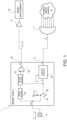
- Figure 1 shows a device 1 of digital type, for example a microcontroller, having a reset pad circuit 2.
- Device 1 may also represent a complex system, for example a system-on-chip, so-called SOC.
- SOC system-on-chip
- the reset pad circuit 2 and the reset structure shown in Figure 1 are generally integrated in a same die, although some parts may be integrated in different dice, as discussed below.
- Reset pad circuit 2 may be easily accessed and localized from the exterior, in order to allow activation of a reset from outside, for example by other devices of the same SOC or other devices operationally coupled thereto.
- Reset pad circuit 2 is coupled to an external access 3 that is configured to receive an external reset request IOFT.
- Reset pad circuit 2 has also an internal reset input 4 configured to receive an internal reset request A.
- Internal reset input 4 may be connected to a plurality of internal resources of the device 1, represented in Figure 1 as a whole as internal reset sources 5.
- Internal reset sources 5 may comprise any circuit, stage, unit, sub-device or even a software/firmware entity that can generate the internal reset request A.
- the internal reset source 5 may include reset sources that may not be or may not completely be integrated or contained in the same die as the reset pad circuit 2.
- Reset pad circuit 2 has also a pad output 10 outputting a reset state signal ZI and coupled, through an input buffer 11, to a portion of the device 1 configured to manage a reset operation, indicated generally as reset manager 12.
- the reset manager 12 may activate a reset operation of the device 1, as defined in a design step.
- reset manager 12 may activate and/or enact protection activities for the device 1 and any resource thereof.
- Reset manager 12 may be integrated in the same die as the reset pad circuit 2 or in a different die, and be coupled thereto through an output pad.
- Reset pad circuit 2 may have a general structure as shown in Figure 1 , where external access 3 is coupled to an input buffer 15 and to a terminal of a biasing element 16.
- Input buffer 15 is coupled to an inverted input of a reset NOR gate 18.
- a glitch filter 19 may be coupled between the input buffer 15 and reset NOR gate 18 to filter out noise existing on external access 3 and that may cause an undesired reset.
- Biasing element 16 is here formed by a transistor 20 that has a conduction terminal coupled to a reference potential line, for example power supply Vcc, through a resistor 21, and to external access 3; a second terminal coupled to another reference potential line, for example ground; and a control terminal coupled to internal reset input 4 through an analog stretch block 22.
- a reference potential line for example power supply Vcc
- Analog stretch block 22 may be any digital block or circuit that stretches the pulse length of the internal reset request A received on the internal reset input 4 to allow a sufficient time to perform reset (for example at least 20 ⁇ s).
- Stretched internal reset signal generated by analog stretch block 22 is indicated in the drawings by A'.
- control terminal of transistor 20 and the output of analog stretch block 22 are coupled to a second, straight (not inverted), input of reset NOR gate 18.
- the reset NOR gate 18 switches to low and passes this information, through reset state signal ZI, to the reset manager 12, that activates the reset procedure as well as any protection activity.
- reset request IOFT switches again to high, the circuit returns to the inactive state.
- the information of the reset state is propagated to the external access 3 by switching on of transistor 20 that causes external access 3 to switch to low state, thereby generating an information that an internal reset request is present, if useful.
- an attack on the reset pad circuit 2, which, as said, is easily accessed from the outside, may cause a disrupt of the standard operations and may jeopardise the device.
- an attack may cause the voltage level on the external access 3 to be unstable or undefined; propagation of this condition to the reset manager 12 may prevent activation of the reset procedure or cause invalidation of security actions based on system reset. If this happens while the device or system clock is running, this may cause execution of possible hacked firmware.
- Figure 2 shows a device 50 that avoids the above possible risky condition.
- Device 50 operates to assert the system reset independently from any state or condition on the reset pad circuit by introducing a by-pass path that anticipates the reset request to the reset manager 12.
- device 50 operates to maintain the reset condition, as started internally, until the reset condition progresses and is fed back by the external reset asserting path.
- device 50 is configured to allow saving of the system reset condition activated by an internal request during an external attack on the reset pad circuit, thus avoiding unstable or undefined states to the reset manager 12.
- device 50 is a digital device, analogously to device 1 of Figure 1 .
- Device 50 has a reset pad circuit 52 that may have the same structure as reset pad circuit 2 of Figure 1 . Therefore, parts of the device 50 corresponding to parts of the device 1 of Figure 1 have been designated with reference numbers increased by 50.
- reset pad circuit 52 includes an input buffer 65, a glitch filter 69, a reset NOR gate 68, an analog stretch block 72 (supplying stretched internal reset signal A'), a transistor 70 and a resistor 71, coupled as above described for the corresponding elements of Figure 1 ; transistor 70 forming a biasing element 66.
- Input buffer 65 (when present), glitch filter 69 and reset NOR gate 68 form a reset request propagating portion.
- Reset pad circuit 52 also has an external (input/output) access 53, receiving external reset request IOFT; an internal reset input 54, receiving an internal reset request A, and a reset pad output 60, outputting a reset state signal ZI (also called feedback reset state signal ZI).
- an external (input/output) access 53 receiving external reset request IOFT
- an internal reset input 54 receiving an internal reset request A
- a reset pad output 60 outputting a reset state signal ZI (also called feedback reset state signal ZI).
- ZI also called feedback reset state signal ZI
- device 50 has an internal resource OR gate 57 coupled to at least one, here a plurality of internal reset sources 55.
- Internal resource OR gate 57 forming an internal reset activation gate, may be integrated or not in the same die as reset pad circuit 52, analogously to what described for device 1 of Figure 1 .
- internal reset sources may include devices able to detect specific attacks; a software application; a watchdog in case the device 50 does not react anymore and other similar devices/applications.
- the internal resource OR gate 57 has its output (supplying internal reset signal IRS) coupled to a flip-flop 75 and to a feedback OR gate 76.
- Flip-flop 75 forms a memory, shadow register and acts as a reset keeper in case of damage of the reset pad circuit 52.
- flip-flop 75 acts to save a system reset instruction from only internal requests during an external attack on the reset pad circuit.
- Flip-flop 75 is a D-type flip-flop, having a data input 75A; a reset (asynchronous) input 75B; a set (inverted, asynchronous) input 75C; and an output 75D.
- Data input 75A is coupled to a reference potential line, here ground.
- Reset input 75B is coupled to the output of internal resource OR gate 57.
- Set input 75C is coupled to reset pad output 60.
- Output 75D of the flip-flop 75 (which supplies a secure reset signal SE_R, also called second reset state signal) is coupled to a first input of an AND gate 77; AND gate 77 has a second input coupled to reset pad output 60.
- AND gate 77 forms a reset forwarding gate and has an output 78 supplying a system reset signal SY_R.
- output 78 of AND gate 77 is coupled to a reset manager 62, that may be integrated in the same die as the reset pad circuit 52 or not, depending on the system design, and may comprise any hardware and/or software resource, as above discussed for device 1.
- Feedback OR gate 76 (forming an internal reset maintaining unit) has here a first (straight/not inverted) input coupled to the output of internal resource OR gate 57; a second (inverted) input coupled to output 75D of flip-flop 75; and an output (supplying the internal reset request A) coupled to internal reset input 54 of reset pad circuit 52.
- Device 50 operates as below discussed in detail, making also reference to Figure 3 , wherein times are not in scale and only represent the sequence of switching operations in device 50.
- Device 50 operates analogously to device 1 of Figure 1 in case of external reset (times t1-t6).
- the device 50 At time t0, in absence of any reset request ("idle state" of the reset portion), the device 50 is in a standard operative condition and the reset portion shown in Figure 2 is inactive.
- external reset request IOFT, reset state signal ZI, secure reset signal SE_R, and system reset signal SY_R are high, while internal reset signal IRS, internal reset request A and stretched internal reset signal A' are low.
- reset is ended and the device 50 returns back in its idle state.
- reset state signal ZI and system reset signal SY_R switch again to high.
- switching of internal reset signal IRS causes commutation of internal reset request A to high (this switching occurring independently from, but at about the same time as switching of secure reset signal SE_R and thus has been indicated in Figure 3 at the same time t8).
- stretched internal reset signal A' also switches to high, activating the reset pad circuit 52, as discussed below.
- the reset manager 12 activates all the actions connected with a reset state, including stopping all the operations of the various units/parts of device 50, including the internal reset source 55 that has started the reset procedure (except, of course, any parts that have been specifically designed to operate in reset condition).
- transistor 70 is turned on by stretched internal reset signal A' and causes external access 53 to go low (external reset request IOFT goes to "0"). Thus, any external resource coupled to external access 53 is informed of the reset state of device 50.
- the high level of stretched internal reset signal A' is also propagated to reset NOR gate 68, that causes reset state signal ZI to switch to low (also indicated at time t11, although generally not occurring simultaneous with switching of external reset request IOFT to low; generally occurring earlier).
- the device 50 is thus again in operative condition and the reset portion of Figure 2 is in the state discussed with reference to time t0.
- Figure 4 shows a digital device 80, wherein the output of internal resource OR gate 57 is directly connected to internal reset input 54 and thus no feedback connection exists from the output 75D of flip-flop 75.
- Digital device 80 has a similar behavior as discussed above with reference to Figure 3 .
- internal reset signal IRS switches to high, causing commutation of flip-flop 75; secure reset signal SE_R switches to low, causing also system reset signal SY_R to switch to low and to activate a reset operation.
- Propagation of the activation pulse of stretched internal reset signal A' to reset NOR gate 68 causes reset state signal ZI to switch to low and confirm a reset request at the second input of AND gate 77.
- This solution may be used when the reset request from the one of the internal reset sources 55 is maintained for a sufficient time to activate its propagation from the internal reset input 54 to the reset pad output 60 while system reset signal SY_R is already active (previously activated by flip-flop 75).
- FIG. 2-4 operate well in protecting devices 50 and 80 and activating a reset procedure when an internal request is received, as above demonstrated.
- the devices 50 and 80 are not completely protected; in particular this may happen when reset pad circuit 52 is damaged or even destroyed by an outside attack.
- external reset request IOFT and reset state signal ZI may be floating, thus set input 75C is floating, causing also secure reset signal SE_R and system reset signal SY_R to be floating.
- SE_R and system reset signal SY_R secure reset signal
- the embodiment of Figure 5 may be used, comprising a state keeping element that stores the level existing at the output of reset NOR gate 68 and is refreshed cyclically; in particular, when the device 50 operates correctly, reset state signal ZI adjourns the state of the state keeping element.
- Figure 5 shows a device 100 that has the same general structure as device 50 of Figure 2 , thus corresponding elements have been indicated with the same reference numbers.
- Device 100 includes a state keeping element 101 coupled to set input 75C of flip-flop 75 and possibly arranged in close proximity thereto, for example at a distance of a few nanometers.
- State keeping element 101 is formed for example by a bus-keeper, comprising here two inverters 102, that are antiparallel coupled.
- state keeping element 101 maintains the last logic value of reset state signal ZI.
- flip-flop 75 may be replaced by a temporary memory element.
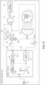
- Figure 6 shows a device 150 with the same general structure as device 50 of Figure 2 (thus, corresponding elements have been indicated with the same reference numbers), wherein flip-flop 75 has been replaced by a latch (L) 151.
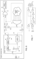
- latch 151 may be implemented as shown in Figure 7 .
- Latch 151 has a data input 151A (corresponding to input D of Figure 7 ) coupled to ground; reset input 151B (corresponding to clock input Clk in Figure 7 ) coupled to the output of internal resource OR gate 57; a set input 151C (corresponding to inverted reset input Rst in Figure 7 ) coupled to output of reset NOR gate 68; and an output 151D (corresponding to output Q in Figure 7 ) coupled to the first input of AND gate 77 and to inverted input of feedback OR gate 76 and supplying secure reset signal SE_R.
- latch 151 Since a latch is level, rather than edge sensitive, latch 151 does not switch in case of metastability on its set input 151C and there is a higher probability that any level instability at the output of reset NOR gate 68 is resolved before latch closure.
- latch 151 confirms a reset state by maintaining a high value at its output 151D; if not, it remains at its previous level and switches only when an internal reset source 55 activates the reset phase through internal resource OR gate 57.
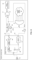
- Figure 8 shows a device 200 using a memory element where the reset input has priority on the set input; thereby a system reset may be generated by an internal reset source 55, independently on any metastability at the output of the reset pad circuit 52.
- Device 200 of Figure 8 has the same general structure as device 50 of Figure 2 (thus, corresponding elements have been indicated with the same reference numbers and only different parts will be described).
- device 200 comprises a flip-flop 201 of the S/R type, having a data input 201A, coupled to ground; a clock input 201B, also coupled to ground; an (asynchronous) set input 201C; an (asynchronous) reset input 201E coupled to output of internal resource OR gate 57; and an output 201D coupled to the first input of AND gate 77.
- Device 200 has an asynchronous reset AR(reset input 201E) that has priority on asynchronous set (set input 201C) that always allows a system reset assertion.
- asynchronous reset AR(reset input 201E) that has priority on asynchronous set (set input 201C) that always allows a system reset assertion.
- the internal reset signal IRS is maintained until the system reset signal SY_R is propagated internally and the device 200 is able to interrupt the reset condition. Thereby, the device 200 returns back to its default condition.
- the clock input 201C of flip-flop 201 may be connected to any other fixed voltage, for example power supply.
- the digital device may be useful for the digital device to receive a direct in-time information of an existing (possible) attack of the reset pad circuit 52.
- Figure 9 shows a device 250 that allows internal units, for example a central unit 251, to be immediately informed.
- Device 250 is here similar to device 80 of Figure 4 (thus, corresponding elements have been indicated with the same reference numbers) and thus has the output of internal resource OR gate 57 directly coupled to internal reset input 54 of reset pad circuit 52.
- device 250 of Figure 9 also includes state keeping element 101 as in Figure 5 .
- input 75C is an asynchronous reset input; and the output 75D of flip-flop 75 is coupled to a CPU 251, for example of a microcontroller.
- output 75D of flip-flop 75 may be coupled to an inverted input of AND gate 77.
- system reset signal SY_R may cause a pre-alarm situation to all parts, except for the CPU 251, so that the latter is completely operative and may manage the information coming directly, as above discussed.
- Device 250 of Figure 9 is not protected against an attack directed on the flip-flop 75, e.g., using electromagnetic, such as FIB (Focused Ion Beam) attacks which corrupt the output value of flip-flop 75.
- electromagnetic such as FIB (Focused Ion Beam) attacks which corrupt the output value of flip-flop 75.
- a solution for increasing the robustness of a digital device against FIB attacks includes introducing some sort of redundancy.
- Figure 10 shows a device 300 having the general structure of device 250 of Figure 9 (thus, corresponding elements have been indicated with the same reference numbers), but includes a first flip-flop 75.1 and a second flip-flop 75.2.
- input 75C is a reset input.
- First and second flip-flops 75.1, 75.2 have both their inputs 75C (asynchronous set input for first flip-flop 75.1, and asynchronous reset input for second flip-flop 75.2) coupled to the reset pad output 60; their other (clock) input 75B coupled to the output of internal resource OR gate 57; their data input 75A coupled to ground and, respectively, to power supply Vcc; and their outputs 75D coupled to respective inputs of an interrupt request OR gate 302 that is configured to generate an interrupt secure reset signal SE_R_IRQ.
- flip-flops 75.1, 75.2 are configured to have opposed logic set levels (and opposed reset levels).
- first and second flip-flops 75.1, 75.2 generating respective secure reset signal SE_R
- secure reset signal 302 is configured to generate a low level of interrupt secure reset signal SE_R_IRQ also when just one of outputs 75D of flip-flops 75.1, 75.2 switches at its set level (low at first flip-flop 75.1 and high at second flip-flop 75.2).
- interrupt request OR gate 302 is able to receive at least one correct secure reset signal SE_R and cause activation of reset (through interrupt secure reset signal SE_R_IRQ) in case of an attack is detected by any internal source 55.
- device 300 also has a state keeping element 101 for maintaining the last logic value of reset state signal ZI, although this is not mandatory.
- the protection module including first and second flip-flops 75.1, 75.2, interrupt request OR gate 302 and state keeping element 101 is indicated in Figure 10 by reference number 303.
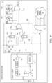
- Figure 11 shows a device 350 having a plurality of protection modules 303 whose outputs are coupled to a global reset OR gate 351 configured to generate a global secure reset signal SE_R_G.
- protection modules 303 each of which may activate a reset procedure
- device 303 has an increased robustness against electromagnetic attacks and also against net cut.
- the plurality of protection modules 303 may be distributed along the path coupling the reset pad output 60 to reset manager 62 (not shown in Figure 11 ), thereby increasing the ability of device 300 to resist to attacks.
- flip-flop 75 may have the data input 75A coupled to a different reference voltage, for example power supply, in which case it may be inverted before being provided to AND gate 77.
- a different reference voltage for example power supply
- a digital device (50; 80; 100; 150; 200; 250; 300; 350), comprising:
- Example 2 A digital device according to example 1, wherein the reset forwarding gate (77) is an AND gate.
- Example 3 A digital device according to example 1 or 2, wherein the internal reset activation gate (57) is an OR gate.
- Example 4 A digital device according to any of preceding examples, wherein the memory element (75; 151; 201; 75.1, 75.2) is a flip-flop or a latch having a reset input forming the first input (75B; 151B; 201B) of the memory element and a set input forming the second input (75C; 151C; 201C) of the memory element.
- Example 5 A digital device according to the preceding example, wherein the flip-flop (75; 201; 75.1, 75.2) is an asynchronous set, asynchronous reset D-type flip-flop (75) having a data input coupled to a reference potential, a clock input coupled to the output of the internal reset activation gate (57) and a set input coupled to the output of reset pad circuit (52), or an S/R flip-flop (201), having a data input and a clock input coupled together and to a reference potential, a reset input coupled to the output of the internal reset activation gate (57) and a set input coupled to the output of reset pad circuit (52).
- the flip-flop (75; 201; 75.1, 75.2 is an asynchronous set, asynchronous reset D-type flip-flop (75) having a data input coupled to a reference potential, a clock input coupled to the output of the internal reset activation gate (57) and a set input coupled to the output of reset pad circuit (52).
- Example 6 A digital device according any of the preceding examples, further comprising an internal reset maintaining unit (76) activated by the internal reset activation gate (57) and confirmed by the memory element (75; 151; 201; 75.1, 75.2), the internal reset maintaining unit (76) configured to generate an internal reset information supplied to the second input of the reset pad circuit (52).
- an internal reset maintaining unit (76) activated by the internal reset activation gate (57) and confirmed by the memory element (75; 151; 201; 75.1, 75.2
- the internal reset maintaining unit (76) configured to generate an internal reset information supplied to the second input of the reset pad circuit (52).
- Example 7 A digital device according to the preceding example, wherein reset maintaining unit (76) is an OR gate having a first input coupled to the output of the internal reset activation gate (57); a second input coupled to the output (75D; 151D; 201D; 75D) of the memory element (75; 151; 201; 75.1, 75.2) and an output directly coupled with the second input (54) of reset pad circuit (52).
- reset maintaining unit (76) is an OR gate having a first input coupled to the output of the internal reset activation gate (57); a second input coupled to the output (75D; 151D; 201D; 75D) of the memory element (75; 151; 201; 75.1, 75.2) and an output directly coupled with the second input (54) of reset pad circuit (52).
- Example 8 A digital device according to any of the preceding examples, further comprising a state keeping element (101) coupled to the second input (75C; 151C; 201C; 75C) of the memory element (75; 151; 201; 75.1, 75.2).
- a state keeping element (101) coupled to the second input (75C; 151C; 201C; 75C) of the memory element (75; 151; 201; 75.1, 75.2).
- Example 9 A digital device according to any of the preceding examples, wherein the output (75D; 151D; 201D) of the memory element (75; 151; 201; 75.1, 75.2) is coupled with a central processing unit (251).
- Example 10 A digital device according to any of the preceding examples, comprising a protective module (303) including:
- Example 11 A digital device according to the preceding example, comprising a plurality of protective modules (303).
- Example 12 A method for activating a reset procedure of a digital device, comprising a reset pad circuit (52); an internal reset activation gate (57); a memory element (75; 151; 201; 75.1, 75.2); and a reset forwarding gate (77), the reset pad having a first (53) and a second (54) input and an output (60), the method comprising:
- Example 13 A method according to the preceding example, wherein deactivating the reset procedure comprises supplying the feedback reset state signal (ZI) to a second input (75C; 151C; 201C; 75C) of the memory element (75; 151; 201; 75.1, 75.2) .
- Example 14 A method according to the preceding example, further comprising storing a logic level of the feedback reset state signal (ZI) on a state keeping element (101) coupled to the second input (75C; 151C; 201C) of the memory element (75; 151; 201; 75.1, 75.2).
- ZI feedback reset state signal
- Example 15 A method according to any of examples 12-14, further comprising generating a reset information on the first input (53) of the reset pad circuit (52) based on the reset request (IRS).
- Example 16 A method according example 12, wherein the memory element (75) directly informs a central processing unit (251), by means of an interrupt line, that an internal reset request is not correctly fed back through the reset pad circuit.
Landscapes
- Engineering & Computer Science (AREA)
- Theoretical Computer Science (AREA)
- Physics & Mathematics (AREA)
- General Engineering & Computer Science (AREA)
- General Physics & Mathematics (AREA)
- Computer Hardware Design (AREA)
- Mathematical Physics (AREA)
- Computer Security & Cryptography (AREA)
- Software Systems (AREA)
- Quality & Reliability (AREA)
- Electronic Switches (AREA)
Abstract
A digital device (50), wherein a reset pad circuit (52) has a first input coupled to a first reset access port (53) configured to receive a first reset request (IOFT), a second input coupled to a second reset access port (54), and an output (60), the reset pad circuit (52) configured to generate a first reset state signal (ZI) and having a reset request propagating portion (65, 68, 72) coupling the second input to the output of the reset pad circuit (52). An internal reset activation gate (57) has a plurality of inputs coupled to internal resources (55) and an output coupled with the second reset access port (54) of reset pad (circuit 52), the internal reset activation gate (57) configured to generate a reset request (IRS). A memory element (75) has a first input (75B) coupled to the output of the internal reset activation gate (57), a second input (75C) coupled to the output (60) of the reset pad circuit (52), and an output (75D), the memory element configured to generate a second reset state signal (SE_R) when receiving the reset request (IRS) until receiving the first reset state signal (ZI). A reset forward gate (77) is coupled to the outputs of the reset pad circuit (52) and the memory element (75) and configured to generate a system reset request (SY_R) in presence of the first reset state signal (ZI) and/or the second state signal (SE_R).
Description
- The present invention relates to a digital device having a reset pad circuit that may be subject to hacker attack.
- As is known, present digital devices, such as microcontrollers, Systems-On-Chip (SOC) and the like often have a pad that is open to the outside for activating a reset operation. For example, this may be useful in certain situations, where it is desired that the device is brought to a known status and/or when the device has to undergo a function interruption, and a re-start of the device is desired.
- A problem with reset pads accessible from the outside is that they may be subject to a hacker attack. Many different attacks are possible, including mechanical attack, chemical attack or focused ion beam attack.
- If an attack occurs when the device is not under reset, serious safety and security problems may occur and may affect the entire device or system they are integrated into.
- In fact, present devices often use the reset condition to perform security activities to avoid any propagation of the attack. However, if the attack is directed against the reset pad circuit and causes a severe damage thereof, the device may not be in a condition to activate the reset procedures and enact safety procedures.
- Thus, an aim of the invention is overcome the drawbacks and limitations of the prior art, by providing a solution able to detect and/or protect the device from attacks directed the reset pad.
- According to the present invention, there are provided a digital device and a method for activating a reset procedure of a digital device, as defined in the attached claims.
- For the understanding of the present invention, embodiments thereof are now described, purely as a non-limitative example, with reference to the enclosed drawings, wherein:
-
Figure 1 is a schematic block diagram of a digital device having a reset pad circuit that may subject to a reset pad circuit attack; -
Figure 2 is a schematic block diagram of an embodiment of the present digital device having a protection portion; -
Figure 3 shows the timing of signals in the digital device ofFigure 2 in two different operational conditions, where times are not in scale; -
Figures 4-6 are schematic block diagrams of other embodiments of the present digital device with a protection portion; -
Figure 7 is a circuit diagram of a possible implementation of a part of the digital device ofFigure 6 ; -
Figure 8 is a schematic block diagram of another embodiment of the present digital device having a protection portion; -
Figure 9 is a schematic block diagrams of a different embodiment of the present digital device having a detection portion; and -
Figures 10 and11 are schematic block diagrams of different embodiments of the present digital device. -
Figure 1 shows a device 1 of digital type, for example a microcontroller, having areset pad circuit 2. Device 1 may also represent a complex system, for example a system-on-chip, so-called SOC. In the latter case, thereset pad circuit 2 and the reset structure shown inFigure 1 are generally integrated in a same die, although some parts may be integrated in different dice, as discussed below. - Reset
pad circuit 2 may be easily accessed and localized from the exterior, in order to allow activation of a reset from outside, for example by other devices of the same SOC or other devices operationally coupled thereto. -
Reset pad circuit 2 is coupled to anexternal access 3 that is configured to receive an external reset request IOFT. -
Reset pad circuit 2 has also aninternal reset input 4 configured to receive an internal reset request A.Internal reset input 4 may be connected to a plurality of internal resources of the device 1, represented inFigure 1 as a whole asinternal reset sources 5. -
Internal reset sources 5 may comprise any circuit, stage, unit, sub-device or even a software/firmware entity that can generate the internal reset request A. - The
internal reset source 5 may include reset sources that may not be or may not completely be integrated or contained in the same die as thereset pad circuit 2. - In
Figure 1 , the requests of theinternal reset sources 5 are fed through an internal resource OR gate 7 having an output coupled tointernal reset input 4 of thereset pad circuit 2. -
Reset pad circuit 2 has also apad output 10 outputting a reset state signal ZI and coupled, through aninput buffer 11, to a portion of the device 1 configured to manage a reset operation, indicated generally asreset manager 12. - As above indicated, the
reset manager 12 may activate a reset operation of the device 1, as defined in a design step. In addition,reset manager 12 may activate and/or enact protection activities for the device 1 and any resource thereof. -
Reset manager 12 may be integrated in the same die as thereset pad circuit 2 or in a different die, and be coupled thereto through an output pad. -
Reset pad circuit 2 may have a general structure as shown inFigure 1 , whereexternal access 3 is coupled to aninput buffer 15 and to a terminal of abiasing element 16. -
Input buffer 15 is coupled to an inverted input of areset NOR gate 18. Aglitch filter 19 may be coupled between theinput buffer 15 and resetNOR gate 18 to filter out noise existing onexternal access 3 and that may cause an undesired reset. -
Biasing element 16 is here formed by atransistor 20 that has a conduction terminal coupled to a reference potential line, for example power supply Vcc, through aresistor 21, and toexternal access 3; a second terminal coupled to another reference potential line, for example ground; and a control terminal coupled tointernal reset input 4 through ananalog stretch block 22. -
Analog stretch block 22 may be any digital block or circuit that stretches the pulse length of the internal reset request A received on theinternal reset input 4 to allow a sufficient time to perform reset (for example at least 20 µs). - Stretched internal reset signal generated by
analog stretch block 22 is indicated in the drawings by A'. - The control terminal of
transistor 20 and the output ofanalog stretch block 22 are coupled to a second, straight (not inverted), input ofreset NOR gate 18. - In the device 1, starting from an inactive or rest state, wherein the
external access 3 is high and theinternal reset input 4 is low, when a reset input is received (falling edge of external reset request IOFT), thereset NOR gate 18 switches to low and passes this information, through reset state signal ZI, to thereset manager 12, that activates the reset procedure as well as any protection activity. When external reset request IOFT switches again to high, the circuit returns to the inactive state. - Analogously, as shown by hatched lines, when an internal reset request A is received at the
internal reset input 4, thereset NOR gate 18 switches to low, activating the reset procedure. The reset state is ended when the stretched internal reset signal A' generated by theanalog stretch block 22 switches back to low. - In addition, in case of generation of an internal reset request, the information of the reset state is propagated to the
external access 3 by switching on oftransistor 20 that causesexternal access 3 to switch to low state, thereby generating an information that an internal reset request is present, if useful. - In the device 1, an attack on the
reset pad circuit 2, which, as said, is easily accessed from the outside, may cause a disrupt of the standard operations and may jeopardise the device. - In addition, internal requests may be lost if an hacker attack damages the
reset pad circuit 2. - In fact, an attack may cause the voltage level on the
external access 3 to be unstable or undefined; propagation of this condition to thereset manager 12 may prevent activation of the reset procedure or cause invalidation of security actions based on system reset. If this happens while the device or system clock is running, this may cause execution of possible hacked firmware. -
Figure 2 shows adevice 50 that avoids the above possible risky condition. -
Device 50 operates to assert the system reset independently from any state or condition on the reset pad circuit by introducing a by-pass path that anticipates the reset request to thereset manager 12. - In addition,
device 50 operates to maintain the reset condition, as started internally, until the reset condition progresses and is fed back by the external reset asserting path. - In particular,
device 50 is configured to allow saving of the system reset condition activated by an internal request during an external attack on the reset pad circuit, thus avoiding unstable or undefined states to thereset manager 12. - In addition, it ensures that an internal reset request is propagated through the reset pad circuit back to the system, also in case of an attack, avoiding the internal request to be lost.
- In detail,
device 50 is a digital device, analogously to device 1 ofFigure 1 . -
Device 50 has areset pad circuit 52 that may have the same structure asreset pad circuit 2 ofFigure 1 . Therefore, parts of thedevice 50 corresponding to parts of the device 1 ofFigure 1 have been designated with reference numbers increased by 50. - In particular,
reset pad circuit 52 includes aninput buffer 65, aglitch filter 69, areset NOR gate 68, an analog stretch block 72 (supplying stretched internal reset signal A'), atransistor 70 and aresistor 71, coupled as above described for the corresponding elements ofFigure 1 ;transistor 70 forming abiasing element 66. - Input buffer 65 (when present),
glitch filter 69 and resetNOR gate 68 form a reset request propagating portion. -
Reset pad circuit 52 also has an external (input/output)access 53, receiving external reset request IOFT; aninternal reset input 54, receiving an internal reset request A, and areset pad output 60, outputting a reset state signal ZI (also called feedback reset state signal ZI). - In addition,
device 50 has an internal resource ORgate 57 coupled to at least one, here a plurality ofinternal reset sources 55. Internal resource ORgate 57, forming an internal reset activation gate, may be integrated or not in the same die asreset pad circuit 52, analogously to what described for device 1 ofFigure 1 . For example, internal reset sources may include devices able to detect specific attacks; a software application; a watchdog in case thedevice 50 does not react anymore and other similar devices/applications. - In
device 50 ofFigure 2 , the internal resource ORgate 57 has its output (supplying internal reset signal IRS) coupled to a flip-flop 75 and to a feedback ORgate 76. - Flip-
flop 75 forms a memory, shadow register and acts as a reset keeper in case of damage of thereset pad circuit 52. In particular, flip-flop 75 acts to save a system reset instruction from only internal requests during an external attack on the reset pad circuit. - Flip-
flop 75 is a D-type flip-flop, having adata input 75A; a reset (asynchronous)input 75B; a set (inverted, asynchronous)input 75C; and anoutput 75D. -
Data input 75A is coupled to a reference potential line, here ground. -
Reset input 75B is coupled to the output of internal resource ORgate 57. - Set
input 75C is coupled to resetpad output 60. -
Output 75D of the flip-flop 75 (which supplies a secure reset signal SE_R, also called second reset state signal) is coupled to a first input of an ANDgate 77; ANDgate 77 has a second input coupled to resetpad output 60. - AND
gate 77 forms a reset forwarding gate and has anoutput 78 supplying a system reset signal SY_R. InFigure 2 ,output 78 of ANDgate 77 is coupled to areset manager 62, that may be integrated in the same die as thereset pad circuit 52 or not, depending on the system design, and may comprise any hardware and/or software resource, as above discussed for device 1. - Feedback OR gate 76 (forming an internal reset maintaining unit) has here a first (straight/not inverted) input coupled to the output of internal resource OR
gate 57; a second (inverted) input coupled tooutput 75D of flip-flop 75; and an output (supplying the internal reset request A) coupled tointernal reset input 54 ofreset pad circuit 52. -
Device 50 operates as below discussed in detail, making also reference toFigure 3 , wherein times are not in scale and only represent the sequence of switching operations indevice 50. -
Device 50 operates analogously to device 1 ofFigure 1 in case of external reset (times t1-t6). - At time t0, in absence of any reset request ("idle state" of the reset portion), the
device 50 is in a standard operative condition and the reset portion shown inFigure 2 is inactive. In particular, external reset request IOFT, reset state signal ZI, secure reset signal SE_R, and system reset signal SY_R are high, while internal reset signal IRS, internal reset request A and stretched internal reset signal A' are low. - At time t1, an external request is applied to
external access 53, by switching external reset request IOFT to low; thus, at time t2, due to commutation of reset NORgate 68, reset state signal ZI also switches to low and, at time t3, due to commutation of ANDgate 77, system reset signal SY_R also switches to low, causingreset manager 62 to initiate a reset operation and to perform any security action provided for indevice 50. - In this period, generally, no reset request from the
internal reset sources 55 is generated; therefore, internal reset signal IRS remains low; and internal resource ORgate 57, flip-flop 75, and feedback ORgate 76 do not change state. - When external reset request IOFT switches back to the high state, reset is ended and the
device 50 returns back in its idle state. In particular, reset state signal ZI and system reset signal SY_R switch again to high. - In case of an internal reset request, when any of the
internal reset resources 55 generates a device reset pulse, internal reset signal IRS switches to high (time t7). - Switching of internal reset signal IRS, at reset (clock)
input 75B, causes flip-flop 75 to change state (time t8), also becauseset input 75C (which has priority, but is active when low) is at high level; thus, secure reset signal SE_R switches to low, causing system reset signal SY_R to switch to low (time t9) and to activate a reset operation. - In addition, switching of internal reset signal IRS causes commutation of internal reset request A to high (this switching occurring independently from, but at about the same time as switching of secure reset signal SE_R and thus has been indicated in
Figure 3 at the same time t8). - At time t9, stretched internal reset signal A' also switches to high, activating the
reset pad circuit 52, as discussed below. - In the meantime, after receiving the system reset signal SY_R, the
reset manager 12 activates all the actions connected with a reset state, including stopping all the operations of the various units/parts ofdevice 50, including theinternal reset source 55 that has started the reset procedure (except, of course, any parts that have been specifically designed to operate in reset condition). - As a consequence, internal reset signal IRS switches to low, time t10. However, flip-
flop 75 does not change state and secure reset signal SE_R remains low, due to the high value of reset state signal ZI. Thus, feedback ORgate 76 is maintained in its state and internal reset request A remains high. - At time t11,
transistor 70 is turned on by stretched internal reset signal A' and causesexternal access 53 to go low (external reset request IOFT goes to "0"). Thus, any external resource coupled toexternal access 53 is informed of the reset state ofdevice 50. - The high level of stretched internal reset signal A' is also propagated to reset NOR
gate 68, that causes reset state signal ZI to switch to low (also indicated at time t11, although generally not occurring simultaneous with switching of external reset request IOFT to low; generally occurring earlier). - System reset signal SY_R is thus confirmed low.
- Switching of the signal (reset state signal ZI) on
set input 75C of flip-flop 75 causes switching of theoutput 75D thereof to high, time t12. However, ANDgate 77 does not change state, due to low level of reset state signal ZI, as said. - Switching of secure reset signal SE_R to high at time t12 causes feedback OR
gate 76 to change state, also due to the low level of internal reset signal IRS; thus internal reset request A switches to low (time t13) and, after a while, also stretched internal reset signal A' switches to low (time t14), causing the end of the reset condition at reset pad circuit 52 (time t15, with external reset request IOFT and reset state signal ZI switching again to high, also here, generally not simultaneously) and, as a consequence, of the entire device 50 (switching of system reset signal SY_R to high, time t16). - The
device 50 is thus again in operative condition and the reset portion ofFigure 2 is in the state discussed with reference to time t0. -
Figure 4 shows adigital device 80, wherein the output of internal resource ORgate 57 is directly connected tointernal reset input 54 and thus no feedback connection exists from theoutput 75D of flip-flop 75. -
Digital device 80 has a similar behavior as discussed above with reference toFigure 3 . - In detail, when an internal reset request is generated by any of the
internal reset sources 55, internal reset signal IRS switches to high, causing commutation of flip-flop 75; secure reset signal SE_R switches to low, causing also system reset signal SY_R to switch to low and to activate a reset operation. - In addition, internal reset request A and stretched internal reset signal A' switch to high, activating the
reset pad circuit 52, analogously to what described above at time t11 ofFigure 3 . - Propagation of the activation pulse of stretched internal reset signal A' to reset NOR
gate 68 causes reset state signal ZI to switch to low and confirm a reset request at the second input of ANDgate 77. - Switching of reset state signal ZI on set
input 75C of flip-flop 75 causes the latter to be set; thereby, secure reset signal SE_R switches again to high, as discussed inFigure 3 at time t12. Also here, due to high level of reset state signal ZI, ANDgate 77 does not change state. - Differently from
device 50 ofFigure 2 , when the reset pulse of internal reset signal IRS ends and internal reset signal IRS switches back to high, after a while, due to the delayed falling edge of internal reset signal A', the reset condition atreset pad circuit 52 ends, with external reset request IOFT and reset state signal ZI switching again to high and, as a consequence, system reset signal SY_R switching to high, analogously to what described with reference toFigure 3 at times t15 and t16. - This solution may be used when the reset request from the one of the
internal reset sources 55 is maintained for a sufficient time to activate its propagation from theinternal reset input 54 to thereset pad output 60 while system reset signal SY_R is already active (previously activated by flip-flop 75). - The solution of
Figure 4 thus effectively protectsdevice 80 in case of an external attack, but is more sensitive to the length of the internal reset signal IRS; in this case, the internal reset signal IRS generated by theinternal reset sources 55 and the delay introduced byanalog stretch block 72 are to be designed to be long enough. - The embodiments of
Figures 2-4 operate well in protectingdevices - In some instances, however, the
devices reset pad circuit 52 is damaged or even destroyed by an outside attack. In this case, in fact, external reset request IOFT and reset state signal ZI may be floating, thus setinput 75C is floating, causing also secure reset signal SE_R and system reset signal SY_R to be floating. A metastability situation thus exists and may be propagated to the rest ofdevice 50 that thus may not operate correctly. - For protecting
device 50 also from the above metastability risk, the embodiment ofFigure 5 may be used, comprising a state keeping element that stores the level existing at the output of reset NORgate 68 and is refreshed cyclically; in particular, when thedevice 50 operates correctly, reset state signal ZI adjourns the state of the state keeping element. -
Figure 5 shows adevice 100 that has the same general structure asdevice 50 ofFigure 2 , thus corresponding elements have been indicated with the same reference numbers. -
Device 100 includes astate keeping element 101 coupled to setinput 75C of flip-flop 75 and possibly arranged in close proximity thereto, for example at a distance of a few nanometers. -
State keeping element 101 is formed for example by a bus-keeper, comprising here twoinverters 102, that are antiparallel coupled. - In case of metastability,
state keeping element 101 maintains the last logic value of reset state signal ZI. - Thus, in presence of an attack of
reset pad circuit 52, this condition may be discovered by aninternal reset source 55 which asserts a reset action through internal reset signal IRS and secure reset signal SE_R; thereby, system reset signal SY_R is still asserted by secure reset signal SE_R and is never released. - This solution works well when the
state keeping element 101 has time to register the state at the output of reset NORgate 68. - According to another solution, flip-
flop 75 may be replaced by a temporary memory element. - For example,
Figure 6 shows adevice 150 with the same general structure asdevice 50 ofFigure 2 (thus, corresponding elements have been indicated with the same reference numbers), wherein flip-flop 75 has been replaced by a latch (L) 151. - For example, latch 151 may be implemented as shown in
Figure 7 . - Latch 151 has a
data input 151A (corresponding to input D ofFigure 7 ) coupled to ground; resetinput 151B (corresponding to clock input Clk inFigure 7 ) coupled to the output of internal resource ORgate 57; aset input 151C (corresponding to inverted reset inputRst inFigure 7 ) coupled to output of reset NORgate 68; and anoutput 151D (corresponding to output Q inFigure 7 ) coupled to the first input of ANDgate 77 and to inverted input of feedback ORgate 76 and supplying secure reset signal SE_R. - Since a latch is level, rather than edge sensitive, latch 151 does not switch in case of metastability on its
set input 151C and there is a higher probability that any level instability at the output of reset NORgate 68 is resolved before latch closure. - In particular, if reset state signal ZI is low, latch 151 confirms a reset state by maintaining a high value at its
output 151D; if not, it remains at its previous level and switches only when aninternal reset source 55 activates the reset phase through internal resource ORgate 57. -
Figure 8 shows adevice 200 using a memory element where the reset input has priority on the set input; thereby a system reset may be generated by aninternal reset source 55, independently on any metastability at the output of thereset pad circuit 52. -
Device 200 ofFigure 8 has the same general structure asdevice 50 ofFigure 2 (thus, corresponding elements have been indicated with the same reference numbers and only different parts will be described). - In detail,
device 200 comprises a flip-flop 201 of the S/R type, having adata input 201A, coupled to ground; aclock input 201B, also coupled to ground; an (asynchronous) setinput 201C; an (asynchronous) resetinput 201E coupled to output of internal resource ORgate 57; and anoutput 201D coupled to the first input of ANDgate 77. -
Device 200 has an asynchronous reset AR(resetinput 201E) that has priority on asynchronous set (setinput 201C) that always allows a system reset assertion. In other words, independently on the signal level of reset state signal ZI (and thus, any presence of metastability), when anyinternal reset source 55 causes generation of a pulse of internal reset signal IRS (e.g., after discovering the metastability), the latter causes starting of a reset phase. - The internal reset signal IRS is maintained until the system reset signal SY_R is propagated internally and the
device 200 is able to interrupt the reset condition. Thereby, thedevice 200 returns back to its default condition. - Two cases may be thus possible:
- 1. The metastability causes the
output 201D of flip-flop 201 to evolve to the rest condition: the reset request initiated by secure reset signal SE_R is cancelled and thedevice 200 exits the reset condition; - 2. The
output 201D of flip-flop 201 does not switch and the device remains in the reset condition until situation above occurs. - Metastability conditions can be thus resolved.
- As an alternative to the solution shown in
Figure 8 , theclock input 201C of flip-flop 201 may be connected to any other fixed voltage, for example power supply. - In certain situations, it may be useful for the digital device to receive a direct in-time information of an existing (possible) attack of the
reset pad circuit 52. -
Figure 9 for example shows adevice 250 that allows internal units, for example acentral unit 251, to be immediately informed. -
Device 250 is here similar todevice 80 ofFigure 4 (thus, corresponding elements have been indicated with the same reference numbers) and thus has the output of internal resource ORgate 57 directly coupled tointernal reset input 54 ofreset pad circuit 52. - In addition,
device 250 ofFigure 9 also includesstate keeping element 101 as inFigure 5 . - In
Figure 9 ,input 75C is an asynchronous reset input; and theoutput 75D of flip-flop 75 is coupled to aCPU 251, for example of a microcontroller. - In addition, the
output 75D of flip-flop 75 may be coupled to an inverted input of ANDgate 77. - With the
device 250 ofFigure 9 , two situations may occur: - 1. Not damaged pad: when internal reset signal IRS switches to high, causing commutation of
output 75D of flip-flop 75 to high, secure reset signal SE_R directly informs theCPU 251 that it will soon receive a reset request, by activating an interrupt. If thereset pad circuit 52 operates correctly, the reset request is activated, the system gets in a default state, the interrupt is cancelled and theCPU 251 starts again from the default state; - 2. Damaged pad: the
CPU 251 receives the interrupt request (high level of internal reset signal IRS) and waits for the system reset. After a delay (that may be configured by software), if no reset request arrives, theCPU 251 may activate corrective measures to protect the device. - In the
device 250, if system reset signal SY_R is generated, it may cause a pre-alarm situation to all parts, except for theCPU 251, so that the latter is completely operative and may manage the information coming directly, as above discussed. -
Device 250 ofFigure 9 , however, is not protected against an attack directed on the flip-flop 75, e.g., using electromagnetic, such as FIB (Focused Ion Beam) attacks which corrupt the output value of flip-flop 75. - A solution for increasing the robustness of a digital device against FIB attacks includes introducing some sort of redundancy.
- For example,
Figure 10 shows adevice 300 having the general structure ofdevice 250 ofFigure 9 (thus, corresponding elements have been indicated with the same reference numbers), but includes a first flip-flop 75.1 and a second flip-flop 75.2. Here,input 75C is a reset input. - First and second flip-flops 75.1, 75.2 have both their
inputs 75C (asynchronous set input for first flip-flop 75.1, and asynchronous reset input for second flip-flop 75.2) coupled to thereset pad output 60; their other (clock)input 75B coupled to the output of internal resource ORgate 57; theirdata input 75A coupled to ground and, respectively, to power supply Vcc; and theiroutputs 75D coupled to respective inputs of an interrupt request ORgate 302 that is configured to generate an interrupt secure reset signal SE_R_IRQ. In practice, flip-flops 75.1, 75.2 are configured to have opposed logic set levels (and opposed reset levels). - The
outputs 75D of first and second flip-flops 75.1, 75.2, generating respective secure reset signal SE_R, are coupled to interrupt request ORgate 302 in an opposite way; in particular, inFigure 10 ,output 75D of first flip-flop 75.1 is inverted. Thus,secure reset signal 302 is configured to generate a low level of interrupt secure reset signal SE_R_IRQ also when just one ofoutputs 75D of flip-flops 75.1, 75.2 switches at its set level (low at first flip-flop 75.1 and high at second flip-flop 75.2). - Accordingly, even if one of first and second flip-flops 75.1, 75.2 is destroyed or damaged by an attack intended to avoid starting a reset operation (with its associated security actions), it is not probable that also the other is; thus, the interrupt request OR
gate 302 is able to receive at least one correct secure reset signal SE_R and cause activation of reset (through interrupt secure reset signal SE_R_IRQ) in case of an attack is detected by anyinternal source 55. - In addition, if an attacker is able to force any logic state on one of the flip-flops 75.1, 75.2, it cannot force two opposite levels. This is also represented in
Figure 10 by signals SE_R1 and SE_R2: if an attacker forces, e.g., a high level, secure reset signal SE_R1 at the output of first flip-flop 75.1 switches, but not secure reset signal SE_R2 at the output of second flip-flop 75.2, thereby interrupt request ORgate 302 is unaffected. - In the embodiment shown in
Figure 10 ,device 300 also has astate keeping element 101 for maintaining the last logic value of reset state signal ZI, although this is not mandatory. - The protection module including first and second flip-flops 75.1, 75.2, interrupt request OR
gate 302 andstate keeping element 101 is indicated inFigure 10 byreference number 303. - The presence of two flip-flops 75.1, 75.2 thus increases robustness of the
device 300 against attacks, for example laser attacks. -
Figure 11 shows adevice 350 having a plurality ofprotection modules 303 whose outputs are coupled to a global reset ORgate 351 configured to generate a global secure reset signal SE_R_G. - By having a plurality of
protection modules 303, each of which may activate a reset procedure,device 303 has an increased robustness against electromagnetic attacks and also against net cut. - Advantageously, the plurality of
protection modules 303 may be distributed along the path coupling thereset pad output 60 to reset manager 62 (not shown inFigure 11 ), thereby increasing the ability ofdevice 300 to resist to attacks. - Of course, the level of redundancy is to be considered in a trade-off with the high requested area.
- Finally, it is clear that numerous variations and modifications may be made to the device described and illustrated herein, all falling within the scope of the invention as defined in the attached claims.
- For example, flip-
flop 75 may have thedata input 75A coupled to a different reference voltage, for example power supply, in which case it may be inverted before being provided to ANDgate 77. - In general, different logic elements, operating on opposed logic level may be envisaged buy the person skilled in the art, for performing the same or similar functions.
- In addition, the various embodiments described above can be combined to provide further embodiments.
- Example embodiments of the present disclosure are summarized hereinbelow.
- Example 1. A digital device (50; 80; 100; 150; 200; 250; 300; 350), comprising:
- a reset pad circuit (52) having a first input coupled to a first reset access port (53) and configured to receive a first reset request (IOFT), a second input coupled to a second reset access port (54), and an output (60), the reset pad circuit (52) configured to generate a first reset state signal (ZI) and having a reset request propagating portion (65, 68, 72) coupling the second input to the output of the reset pad circuit (52);
- an internal reset activation gate (57) having at least one input coupled to an internal resource (55) and an output coupled with the second reset access port (54) of reset pad circuit (52), the internal reset activation gate (57) configured to generate a reset request (IRS);
- a memory element (75; 151; 201; 75.1, 75.2) having a first input (75B; 151B; 201B) coupled to the output of the internal reset activation gate (57), a second input (75C; 151C; 201C) coupled to the output (60) of the reset pad circuit (52), and an output (75D; 151D; 201D; 75D), the memory element configured to generate a second reset state signal (SE_R; SE_R1, SE_R2) when receiving the reset request (IRS) until receiving the first reset state signal (ZI);
- a reset forwarding gate (77) coupled to the outputs of the reset pad circuit (52) and the memory element (75; 151; 201; 75.1, 75.2) and configured to generate a system reset request (SY_R) in presence of the first reset state signal (ZI) and/or the second reset state signal (SE_R; SE_R1, SE_R2).
- Example 2. A digital device according to example 1, wherein the reset forwarding gate (77) is an AND gate.
- Example 3. A digital device according to example 1 or 2, wherein the internal reset activation gate (57) is an OR gate.
- Example 4. A digital device according to any of preceding examples, wherein the memory element (75; 151; 201; 75.1, 75.2) is a flip-flop or a latch having a reset input forming the first input (75B; 151B; 201B) of the memory element and a set input forming the second input (75C; 151C; 201C) of the memory element.
- Example 5. A digital device according to the preceding example, wherein the flip-flop (75; 201; 75.1, 75.2) is an asynchronous set, asynchronous reset D-type flip-flop (75) having a data input coupled to a reference potential, a clock input coupled to the output of the internal reset activation gate (57) and a set input coupled to the output of reset pad circuit (52), or an S/R flip-flop (201), having a data input and a clock input coupled together and to a reference potential, a reset input coupled to the output of the internal reset activation gate (57) and a set input coupled to the output of reset pad circuit (52).
- Example 6. A digital device according any of the preceding examples, further comprising an internal reset maintaining unit (76) activated by the internal reset activation gate (57) and confirmed by the memory element (75; 151; 201; 75.1, 75.2), the internal reset maintaining unit (76) configured to generate an internal reset information supplied to the second input of the reset pad circuit (52).
- Example 7. A digital device according to the preceding example, wherein reset maintaining unit (76) is an OR gate having a first input coupled to the output of the internal reset activation gate (57); a second input coupled to the output (75D; 151D; 201D; 75D) of the memory element (75; 151; 201; 75.1, 75.2) and an output directly coupled with the second input (54) of reset pad circuit (52).
- Example 8. A digital device according to any of the preceding examples, further comprising a state keeping element (101) coupled to the second input (75C; 151C; 201C; 75C) of the memory element (75; 151; 201; 75.1, 75.2).
- Example 9. A digital device according to any of the preceding examples, wherein the output (75D; 151D; 201D) of the memory element (75; 151; 201; 75.1, 75.2) is coupled with a central processing unit (251).
- Example 10. A digital device according to any of the preceding examples, comprising a protective module (303) including:
- the memory element, forming a first memory element (75.1) and configured to generate an own second reset state signal (SE_R1);
- a second memory element (75.2), the second memory element having a first input (75B) coupled to the output (60) of the internal reset activation gate (57), a second input (75C) coupled to the output (60) of the reset pad circuit (52), and an output (75D), the second memory element configured to generate an own second reset state signal (SE_R2) of an opposite logical level than the second reset state signal (SE_R1) of first memory element (75.1) when receiving the reset request (IRS) until receiving the first reset state signal (ZI); and
- an interrupt gate (302) having a first and a second inputs coupled to the outputs of the first and second memory elements and an output configured to generate a system reset in presence of the second reset state signal (SE_R1) of first memory element (75.1) and/or of the second memory element (75.2).
- Example 11. A digital device according to the preceding example, comprising a plurality of protective modules (303).
- Example 12. A method for activating a reset procedure of a digital device, comprising a reset pad circuit (52); an internal reset activation gate (57); a memory element (75; 151; 201; 75.1, 75.2); and a reset forwarding gate (77), the reset pad having a first (53) and a second (54) input and an output (60), the method comprising:
- generating a reset request (IRS) by the internal reset activation gate (57);
- forwarding the reset request (IRS) to a first input (75B; 151B; 201B; 75B) of the memory element (75; 151; 201; 75.1, 75.2) and to the second input (54) of reset pad;
- generating, by the memory element, a reset state signal (SE_R; SE_R1, SE_R2) when receiving the reset request (IRS);
- activating, by the reset forwarding gate (77), a reset procedure upon receiving the reset state signal (SE_R; SE_R1, SE_R2) ;
- propagating the reset request (IRS) in the reset pad circuit (52) to generate a feedback reset state signal (ZI); and
- deactivating, by the reset forwarding gate (77), the reset procedure upon receiving the feedback reset state signal (ZI).
- Example 13. A method according to the preceding example, wherein deactivating the reset procedure comprises supplying the feedback reset state signal (ZI) to a second input (75C; 151C; 201C; 75C) of the memory element (75; 151; 201; 75.1, 75.2) .
- Example 14. A method according to the preceding example, further comprising storing a logic level of the feedback reset state signal (ZI) on a state keeping element (101) coupled to the second input (75C; 151C; 201C) of the memory element (75; 151; 201; 75.1, 75.2).
- Example 15. A method according to any of examples 12-14, further comprising generating a reset information on the first input (53) of the reset pad circuit (52) based on the reset request (IRS).
- Example 16. A method according example 12, wherein the memory element (75) directly informs a central processing unit (251), by means of an interrupt line, that an internal reset request is not correctly fed back through the reset pad circuit.
Claims (15)
- A digital device (50; 80; 100; 150; 200; 250; 300; 350), comprising:a reset pad circuit (52) having a first input coupled to a first input/output reset access port (53) and configured to receive a first reset request (IOFT), a second input coupled to a second reset access port (54), and an output (60), the reset pad circuit (52) configured to generate a first reset state signal (ZI) and having a reset request propagating portion (65, 68, 72) coupling the second input to the output of the reset pad circuit (52);an internal reset activation gate (57) having at least one input coupled to an internal resource (55) and an output coupled to the second reset access port (54) of reset pad circuit (52), the internal reset activation gate (57) configured to generate a reset request (IRS);a memory element (75; 151; 201; 75.1, 75.2) having a first input (75B; 151B; 201B) coupled to the output of the internal reset activation gate (57), a second input (75C; 151C; 201C) coupled to the output (60) of the reset pad circuit (52), and an output (75D; 151D; 201D; 75D), the memory element configured to generate a second reset state signal (SE_R; SE_R1, SE_R2) when receiving the reset request (IRS) until receiving the first reset state signal (ZI);a reset forwarding gate (77) coupled to the outputs of the reset pad circuit (52) and the memory element (75; 151; 201; 75.1, 75.2) and configured to generate a system reset request (SY_R) in presence of the first reset state signal (ZI) and/or the second reset state signal (SE_R; SE_R1, SE_R2) .
- A digital device according to claim 1, wherein the reset forwarding gate (77) is an AND gate.
- A digital device according to claim 1 or 2, wherein the internal reset activation gate (57) is an OR gate.
- A digital device according to any of preceding claims, wherein the memory element (75; 151; 201; 75.1, 75.2) is a flip-flop or a latch having a reset input forming the first input (75B; 151B; 201B) of the memory element and a set input forming the second input (75C; 151C; 201C) of the memory element.
- A digital device according to the preceding claim, wherein the flip-flop (75; 201; 75.1, 75.2) is an asynchronous set, asynchronous reset D-type flip-flop (75) having a data input coupled to a reference potential, a clock input coupled to the output of the internal reset activation gate (57) and a set input coupled to the output of reset pad circuit (52), or an S/R flip-flop (201), having a data input and a clock input coupled together and to a reference potential, a reset input coupled to the output of the internal reset activation gate (57) and a set input coupled to the output of reset pad circuit (52).
- A digital device according any of the preceding claims, further comprising an internal reset maintaining unit (76) activated by the internal reset activation gate (57) and confirmed by the memory element (75; 151; 201; 75.1, 75.2), the internal reset maintaining unit (76) configured to generate an internal reset information supplied to the second input of the reset pad circuit (52).
- A digital device according to the preceding claim, wherein reset maintaining unit (76) is an OR gate having a first input coupled to the output of the internal reset activation gate (57); a second input coupled to the output (75D; 151D; 201D; 75D) of the memory element (75; 151; 201; 75.1, 75.2) and an output directly coupled with the second input (54) of reset pad circuit (52).
- A digital device according to any of the preceding claims, further comprising a state keeping element (101) coupled to the second input (75C; 151C; 201C; 75C) of the memory element (75; 151; 201; 75.1, 75.2).
- A digital device according to any of the preceding claims, wherein the output (75D; 151D; 201D) of the memory element (75; 151; 201; 75.1, 75.2) is coupled with a central processing unit (251).
- A digital device according to any of the preceding claims, comprising a protective module (303) including:the memory element, forming a first memory element (75.1) and configured to generate an own second reset state signal (SE_R1);a second memory element (75.2), the second memory element having a first input (75B) coupled to the output (60) of the internal reset activation gate (57), a second input (75C) coupled to the output (60) of the reset pad circuit (52), and an output (75D), the second memory element configured to generate an own second reset state signal (SE_R2) of an opposite logical level than the second reset state signal (SE_R1) generated by the first memory element (75.1) when receiving the reset request (IRS) until receiving the first reset state signal (ZI); andan interrupt gate (302) having a first input and a second input coupled, respectively, to outputs of the first and second memory elements and an output configured to generate a system reset in response to the second reset state signal (SE_R1) generated by the first memory element (75.1) and/or the second memory element (75.2).
- A digital device according to the preceding claim, comprising a plurality of protective modules (303).
- A method for activating a reset procedure of a digital device comprising a reset pad circuit (52); an internal reset activation gate (57); a memory element (75; 151; 201; 75.1, 75.2); and a reset forwarding gate (77), the reset pad circuit having a first (53) and a second (54) input and an output (60), the method comprising:generating a reset request (IRS) by the internal reset activation gate (57);forwarding the reset request (IRS) to a first input (75B; 151B; 201B; 75B) of the memory element (75; 151; 201; 75.1, 75.2) and to the second input (54) of reset pad;generating, by the memory element, a reset state signal (SE_R; SE_R1, SE_R2) in response to receipt of the reset request (IRS);activating, by the reset forwarding gate (77), a reset procedure in response to receipt of the reset state signal (SE_R; SE_R1, SE_R2);propagating the reset request (IRS) in the reset pad circuit (52) to generate a feedback reset state signal (ZI); anddeactivating, by the reset forwarding gate (77), the reset procedure in response to receipt of the feedback reset state signal (ZI).
- A method according to the preceding claim, wherein disactivating the reset procedure comprises supplying the feedback reset state signal (ZI) to a second input (75C; 151C; 201C; 75C) of the memory element (75; 151; 201; 75.1, 75.2) .
- A method according to the preceding claim, further comprising storing a logic level of the feedback reset state signal (ZI) on a state keeping element (101) coupled to the second input (75C; 151C; 201C) of the memory element (75; 151; 201; 75.1, 75.2).
- A method according to any of claims 12-14, further comprising generating a reset information on the first input (53) of the reset pad circuit (52) based on the reset request (IRS).
Applications Claiming Priority (1)
| Application Number | Priority Date | Filing Date | Title |
|---|---|---|---|
| IT202300000327 | 2023-01-12 |
Publications (1)
| Publication Number | Publication Date |
|---|---|
| EP4400939A1 true EP4400939A1 (en) | 2024-07-17 |
Family
ID=85685809
Family Applications (1)
| Application Number | Title | Priority Date | Filing Date |
|---|---|---|---|
| EP24305015.0A Pending EP4400939A1 (en) | 2023-01-12 | 2024-01-05 | Digital device having a reset pad circuit that may be subject to hacker attack |
Country Status (2)
| Country | Link |
|---|---|
| US (1) | US12586622B2 (en) |
| EP (1) | EP4400939A1 (en) |
Families Citing this family (1)
| Publication number | Priority date | Publication date | Assignee | Title |
|---|---|---|---|---|
| FR3145431B1 (en) * | 2023-01-27 | 2025-10-17 | St Microelectronics Int Nv | Reset circuit |
Citations (5)
| Publication number | Priority date | Publication date | Assignee | Title |
|---|---|---|---|---|
| US5748948A (en) * | 1994-09-10 | 1998-05-05 | Holtek Microelectronics Inc. | Reset signal generator |
| CN205263743U (en) * | 2015-12-22 | 2016-05-25 | 无锡芯响电子科技有限公司 | Controllable reset circuit of bandwidth is released in step to asynchronous reseing |
| US20170061137A1 (en) * | 2014-09-08 | 2017-03-02 | Arm Limited | Apparatus and method for providing resilience to attacks on reset of the apparatus |
| CN105404374B (en) * | 2015-11-06 | 2018-11-02 | 中国电子科技集团公司第四十四研究所 | Reset system and repositioning method in the piece of on-chip system chip |
| US20210192089A1 (en) * | 2019-12-20 | 2021-06-24 | Arm Limited | Security measures for signal paths with tree structures |
Family Cites Families (6)
| Publication number | Priority date | Publication date | Assignee | Title |
|---|---|---|---|---|
| US7586350B2 (en) * | 2005-09-28 | 2009-09-08 | Hynix Semiconductor Inc. | Circuit and method for initializing an internal logic unit in a semiconductor memory device |
| US8601254B1 (en) * | 2009-04-30 | 2013-12-03 | Cypress Semiconductor Corp. | Configurable reset pin for input/output port |
| KR101962907B1 (en) * | 2012-06-28 | 2019-03-28 | 에스케이하이닉스 주식회사 | Integrated circuit chip and memory device |
| KR102070203B1 (en) * | 2012-08-29 | 2020-01-29 | 에스케이하이닉스 주식회사 | Semiconductor Memory Apparatus |
| KR102724327B1 (en) * | 2019-03-29 | 2024-11-01 | 에스케이하이닉스 주식회사 | Semiconductor memory device |
| IT202100007475A1 (en) * | 2021-03-26 | 2022-09-26 | Stmicroelectronics Application Gmbh | COMPUTING SYSTEM, RELATED INTEGRATED CIRCUIT, DEVICE AND PROCEDURE |
-
2024
- 2024-01-05 EP EP24305015.0A patent/EP4400939A1/en active Pending
- 2024-01-11 US US18/410,049 patent/US12586622B2/en active Active
Patent Citations (5)
| Publication number | Priority date | Publication date | Assignee | Title |
|---|---|---|---|---|
| US5748948A (en) * | 1994-09-10 | 1998-05-05 | Holtek Microelectronics Inc. | Reset signal generator |
| US20170061137A1 (en) * | 2014-09-08 | 2017-03-02 | Arm Limited | Apparatus and method for providing resilience to attacks on reset of the apparatus |
| CN105404374B (en) * | 2015-11-06 | 2018-11-02 | 中国电子科技集团公司第四十四研究所 | Reset system and repositioning method in the piece of on-chip system chip |
| CN205263743U (en) * | 2015-12-22 | 2016-05-25 | 无锡芯响电子科技有限公司 | Controllable reset circuit of bandwidth is released in step to asynchronous reseing |
| US20210192089A1 (en) * | 2019-12-20 | 2021-06-24 | Arm Limited | Security measures for signal paths with tree structures |
Also Published As
| Publication number | Publication date |
|---|---|
| US12586622B2 (en) | 2026-03-24 |
| US20240242749A1 (en) | 2024-07-18 |
Similar Documents
| Publication | Publication Date | Title |
|---|---|---|
| CA2147568C (en) | Reset circuit of electronic device | |
| TWI801468B (en) | Apparatus, methods, and systems for protecting the security of an electronic device, and related microcontrollers | |
| EP3430627B1 (en) | Controlling a transition between a functional mode and a test mode | |
| US6948103B2 (en) | Watchdog timer and method for detecting abnormal operation of computer, and computer including the timer | |
| US12586622B2 (en) | Digital device having a reset pad circuit that may be subject to hacker attack | |
| US20190050570A1 (en) | Computer resource access control based on the state of a non-accessing component | |
| JP2009532779A (en) | Multi-mode, uniform latency clock generator circuit device | |
| Aliaj et al. | GAROTA: generalized active root-of-trust architecture | |
| JP4294503B2 (en) | Operation mode control circuit, microcomputer including operation mode control circuit, and control system using the microcomputer | |
| CN118332619A (en) | Digital devices with reset pad circuits that could be hacked | |
| US5677891A (en) | Circuitry and method that allows for external control of a data security device | |
| US20250377970A1 (en) | Protection in asynchronous finite state machine | |
| JP3655648B2 (en) | Process switch control device and process control method | |
| CN113535613A (en) | Interrupt controller and method of managing interrupt controller | |
| US10445500B2 (en) | Reset attack detection | |
| EP4664290A2 (en) | Improved root cause analysis (rca) -based node recovery | |
| US6552570B2 (en) | Input circuit with non-delayed time blanking | |
| JP2870083B2 (en) | Microcomputer with built-in watchdog timer | |
| JPH0756774A (en) | Watching timer | |
| US8316017B2 (en) | Apparatus and method for the detection of and recovery from inappropriate bus access in microcontroller circuits | |
| KR100703711B1 (en) | A control signal generator for controlling the operation of the data transfer buffer, a semiconductor device having the control signal generator, and a method for controlling the operation of the transfer buffer | |
| JPH1078920A (en) | Microcomputer | |
| US20150302209A1 (en) | Control apparatus | |
| JP2988139B2 (en) | Interrupt control device | |
| JP5045692B2 (en) | Operation mode control circuit and microcomputer |
Legal Events
| Date | Code | Title | Description |
|---|---|---|---|
| PUAI | Public reference made under article 153(3) epc to a published international application that has entered the european phase |
Free format text: ORIGINAL CODE: 0009012 |
|
| STAA | Information on the status of an ep patent application or granted ep patent |
Free format text: STATUS: REQUEST FOR EXAMINATION WAS MADE |
|
| 17P | Request for examination filed |
Effective date: 20240105 |
|
| AK | Designated contracting states |
Kind code of ref document: A1 Designated state(s): AL AT BE BG CH CY CZ DE DK EE ES FI FR GB GR HR HU IE IS IT LI LT LU LV MC ME MK MT NL NO PL PT RO RS SE SI SK SM TR |
|
| STAA | Information on the status of an ep patent application or granted ep patent |
Free format text: STATUS: EXAMINATION IS IN PROGRESS |
|
| 17Q | First examination report despatched |
Effective date: 20250725 |