EP4398685A2 - Connector cable - Google Patents
Connector cable Download PDFInfo
- Publication number
- EP4398685A2 EP4398685A2 EP24171954.1A EP24171954A EP4398685A2 EP 4398685 A2 EP4398685 A2 EP 4398685A2 EP 24171954 A EP24171954 A EP 24171954A EP 4398685 A2 EP4398685 A2 EP 4398685A2
- Authority
- EP
- European Patent Office
- Prior art keywords
- connector
- cable
- relay substrate
- contact
- inner conductor
- Prior art date
- Legal status (The legal status is an assumption and is not a legal conclusion. Google has not performed a legal analysis and makes no representation as to the accuracy of the status listed.)
- Granted
Links
Images











Classifications
-
- H—ELECTRICITY
- H01—ELECTRIC ELEMENTS
- H01R—ELECTRICALLY-CONDUCTIVE CONNECTIONS; STRUCTURAL ASSOCIATIONS OF A PLURALITY OF MUTUALLY-INSULATED ELECTRICAL CONNECTING ELEMENTS; COUPLING DEVICES; CURRENT COLLECTORS
- H01R9/00—Structural associations of a plurality of mutually-insulated electrical connecting elements, e.g. terminal strips or terminal blocks; Terminals or binding posts mounted upon a base or in a case; Bases therefor
- H01R9/03—Connectors arranged to contact a plurality of the conductors of a multiconductor cable, e.g. tapping connections
- H01R9/05—Connectors arranged to contact a plurality of the conductors of a multiconductor cable, e.g. tapping connections for coaxial cables
- H01R9/0515—Connection to a rigid planar substrate, e.g. printed circuit board
-
- H—ELECTRICITY
- H01—ELECTRIC ELEMENTS
- H01R—ELECTRICALLY-CONDUCTIVE CONNECTIONS; STRUCTURAL ASSOCIATIONS OF A PLURALITY OF MUTUALLY-INSULATED ELECTRICAL CONNECTING ELEMENTS; COUPLING DEVICES; CURRENT COLLECTORS
- H01R13/00—Details of coupling devices of the kinds covered by groups H01R12/70 or H01R24/00 - H01R33/00
- H01R13/646—Details of coupling devices of the kinds covered by groups H01R12/70 or H01R24/00 - H01R33/00 specially adapted for high-frequency, e.g. structures providing an impedance match or phase match
- H01R13/6473—Impedance matching
-
- H—ELECTRICITY
- H01—ELECTRIC ELEMENTS
- H01R—ELECTRICALLY-CONDUCTIVE CONNECTIONS; STRUCTURAL ASSOCIATIONS OF A PLURALITY OF MUTUALLY-INSULATED ELECTRICAL CONNECTING ELEMENTS; COUPLING DEVICES; CURRENT COLLECTORS
- H01R12/00—Structural associations of a plurality of mutually-insulated electrical connecting elements, specially adapted for printed circuits, e.g. printed circuit boards [PCB], flat or ribbon cables, or like generally planar structures, e.g. terminal strips, terminal blocks; Coupling devices specially adapted for printed circuits, flat or ribbon cables, or like generally planar structures; Terminals specially adapted for contact with, or insertion into, printed circuits, flat or ribbon cables, or like generally planar structures
- H01R12/50—Fixed connections
- H01R12/51—Fixed connections for rigid printed circuits or like structures
- H01R12/53—Fixed connections for rigid printed circuits or like structures connecting to cables except for flat or ribbon cables
-
- H—ELECTRICITY
- H01—ELECTRIC ELEMENTS
- H01R—ELECTRICALLY-CONDUCTIVE CONNECTIONS; STRUCTURAL ASSOCIATIONS OF A PLURALITY OF MUTUALLY-INSULATED ELECTRICAL CONNECTING ELEMENTS; COUPLING DEVICES; CURRENT COLLECTORS
- H01R12/00—Structural associations of a plurality of mutually-insulated electrical connecting elements, specially adapted for printed circuits, e.g. printed circuit boards [PCB], flat or ribbon cables, or like generally planar structures, e.g. terminal strips, terminal blocks; Coupling devices specially adapted for printed circuits, flat or ribbon cables, or like generally planar structures; Terminals specially adapted for contact with, or insertion into, printed circuits, flat or ribbon cables, or like generally planar structures
- H01R12/50—Fixed connections
- H01R12/51—Fixed connections for rigid printed circuits or like structures
- H01R12/55—Fixed connections for rigid printed circuits or like structures characterised by the terminals
- H01R12/57—Fixed connections for rigid printed circuits or like structures characterised by the terminals surface mounting terminals
-
- H—ELECTRICITY
- H01—ELECTRIC ELEMENTS
- H01R—ELECTRICALLY-CONDUCTIVE CONNECTIONS; STRUCTURAL ASSOCIATIONS OF A PLURALITY OF MUTUALLY-INSULATED ELECTRICAL CONNECTING ELEMENTS; COUPLING DEVICES; CURRENT COLLECTORS
- H01R13/00—Details of coupling devices of the kinds covered by groups H01R12/70 or H01R24/00 - H01R33/00
- H01R13/40—Securing contact members in or to a base or case; Insulating of contact members
-
- H—ELECTRICITY
- H01—ELECTRIC ELEMENTS
- H01R—ELECTRICALLY-CONDUCTIVE CONNECTIONS; STRUCTURAL ASSOCIATIONS OF A PLURALITY OF MUTUALLY-INSULATED ELECTRICAL CONNECTING ELEMENTS; COUPLING DEVICES; CURRENT COLLECTORS
- H01R13/00—Details of coupling devices of the kinds covered by groups H01R12/70 or H01R24/00 - H01R33/00
- H01R13/46—Bases; Cases
-
- H—ELECTRICITY
- H01—ELECTRIC ELEMENTS
- H01R—ELECTRICALLY-CONDUCTIVE CONNECTIONS; STRUCTURAL ASSOCIATIONS OF A PLURALITY OF MUTUALLY-INSULATED ELECTRICAL CONNECTING ELEMENTS; COUPLING DEVICES; CURRENT COLLECTORS
- H01R13/00—Details of coupling devices of the kinds covered by groups H01R12/70 or H01R24/00 - H01R33/00
- H01R13/46—Bases; Cases
- H01R13/502—Bases; Cases composed of different pieces
-
- H—ELECTRICITY
- H01—ELECTRIC ELEMENTS
- H01R—ELECTRICALLY-CONDUCTIVE CONNECTIONS; STRUCTURAL ASSOCIATIONS OF A PLURALITY OF MUTUALLY-INSULATED ELECTRICAL CONNECTING ELEMENTS; COUPLING DEVICES; CURRENT COLLECTORS
- H01R13/00—Details of coupling devices of the kinds covered by groups H01R12/70 or H01R24/00 - H01R33/00
- H01R13/648—Protective earth or shield arrangements on coupling devices, e.g. anti-static shielding
-
- H—ELECTRICITY
- H01—ELECTRIC ELEMENTS
- H01R—ELECTRICALLY-CONDUCTIVE CONNECTIONS; STRUCTURAL ASSOCIATIONS OF A PLURALITY OF MUTUALLY-INSULATED ELECTRICAL CONNECTING ELEMENTS; COUPLING DEVICES; CURRENT COLLECTORS
- H01R13/00—Details of coupling devices of the kinds covered by groups H01R12/70 or H01R24/00 - H01R33/00
- H01R13/648—Protective earth or shield arrangements on coupling devices, e.g. anti-static shielding
- H01R13/658—High frequency shielding arrangements, e.g. against EMI [Electro-Magnetic Interference] or EMP [Electro-Magnetic Pulse]
- H01R13/6591—Specific features or arrangements of connection of shield to conductive members
- H01R13/6592—Specific features or arrangements of connection of shield to conductive members the conductive member being a shielded cable
-
- H—ELECTRICITY
- H01—ELECTRIC ELEMENTS
- H01R—ELECTRICALLY-CONDUCTIVE CONNECTIONS; STRUCTURAL ASSOCIATIONS OF A PLURALITY OF MUTUALLY-INSULATED ELECTRICAL CONNECTING ELEMENTS; COUPLING DEVICES; CURRENT COLLECTORS
- H01R13/00—Details of coupling devices of the kinds covered by groups H01R12/70 or H01R24/00 - H01R33/00
- H01R13/648—Protective earth or shield arrangements on coupling devices, e.g. anti-static shielding
- H01R13/658—High frequency shielding arrangements, e.g. against EMI [Electro-Magnetic Interference] or EMP [Electro-Magnetic Pulse]
- H01R13/6591—Specific features or arrangements of connection of shield to conductive members
- H01R13/6594—Specific features or arrangements of connection of shield to conductive members the shield being mounted on a PCB and connected to conductive members
-
- H—ELECTRICITY
- H05—ELECTRIC TECHNIQUES NOT OTHERWISE PROVIDED FOR
- H05K—PRINTED CIRCUITS; CASINGS OR CONSTRUCTIONAL DETAILS OF ELECTRIC APPARATUS; MANUFACTURE OF ASSEMBLAGES OF ELECTRICAL COMPONENTS
- H05K2201/00—Indexing scheme relating to printed circuits covered by H05K1/00
- H05K2201/10—Details of components or other objects attached to or integrated in a printed circuit board
- H05K2201/10007—Types of components
- H05K2201/10189—Non-printed connector
-
- H—ELECTRICITY
- H05—ELECTRIC TECHNIQUES NOT OTHERWISE PROVIDED FOR
- H05K—PRINTED CIRCUITS; CASINGS OR CONSTRUCTIONAL DETAILS OF ELECTRIC APPARATUS; MANUFACTURE OF ASSEMBLAGES OF ELECTRICAL COMPONENTS
- H05K2201/00—Indexing scheme relating to printed circuits covered by H05K1/00
- H05K2201/10—Details of components or other objects attached to or integrated in a printed circuit board
- H05K2201/10227—Other objects, e.g. metallic pieces
- H05K2201/10356—Cables
-
- H—ELECTRICITY
- H05—ELECTRIC TECHNIQUES NOT OTHERWISE PROVIDED FOR
- H05K—PRINTED CIRCUITS; CASINGS OR CONSTRUCTIONAL DETAILS OF ELECTRIC APPARATUS; MANUFACTURE OF ASSEMBLAGES OF ELECTRICAL COMPONENTS
- H05K3/00—Apparatus or processes for manufacturing printed circuits
- H05K3/30—Assembling printed circuits with electric components, e.g. with resistors
- H05K3/32—Assembling printed circuits with electric components, e.g. with resistors electrically connecting electric components or wires to printed circuits
- H05K3/34—Assembling printed circuits with electric components, e.g. with resistors electrically connecting electric components or wires to printed circuits by soldering
- H05K3/3405—Edge mounted components, e.g. terminals
Definitions
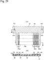
- Japanese Patent Laid-Open No. 8-167457 discloses a conventional example of a high-speed connector cable in which contacts (3) of electric connectors (1) are connected to coaxial cables (5) via relay substrates (4), as shown in FIGS. 27 to 30 .
- the high-speed connector cable disclosed in Japanese Patent Laid-Open No. 8-167457 discloses a conventional example of a high-speed connector cable in which contacts (3) of electric connectors (1) are connected to coaxial cables (5) via relay substrates (4), as shown in FIGS. 27 to 30 .
- a connector cable 100 of the first embodiment includes a connector 10, a shielded cable 20, and a relay substrate 30.
- the connector cable 100 has a configuration in which the connector 10 and the shielded cable 20 are connected via the relay substrate 30.
- the first embodiment has a configuration such that: the GND conductor layer 32 on the front surface of the relay substrate 30 extends to a position directly under the contact 111 for high-speed signals of the connector 10 and the exposed inner conductor 21 of the shielded cable 20; and the GND conductor layer 32 on the front surface of the relay substrate 30, which extends to the positions directly under the contact 111 for high-speed signals of the connector 10 and the exposed inner conductor 21 of the shielded cable 20, is also covered with the insulating member 31 made of a resist.
- the following describes the detailed structure of the connector cable 100 of the first embodiment with reference to FIG. 4 .
- soldering the shield member 23 of the shielded cable 20 to the GND conductor layer 32 on the front surface of the relay substrate 30 brings about effects such as noise prevention.
- the GND conductor layer 32 on the front surface of the relay substrate 30 is arranged at a position directly under the shield member 23 in a state in which the GND conductor layer 32 is not covered with the insulating member 31 made of a resist.
- the GND conductor layer 32 on the front surface of the relay substrate 30 has a boundary at a position indicated by reference character C in FIG. 4 .
- the one side of the boundary, where the connector 10 is arranged, is coated with an insulating member 31 made of a resist, and the other side thereof, where the shield member 23 of the shielded cable 20 is located, is not coated with an insulating member 31 made of a resist.
- the connection part between the contact 111 for high-speed signals of the connector 10 and the exposed inner conductor 21 of the shielded cable 20 is connected by soldering, as in the case of the first embodiment described above.
- the connector cable 200 of the second embodiment has the GND conductor layer 32 on the front surface of the relay substrate 30.
- the GND conductor layer 32 located directly under the connection part between the contact 111 for high-speed signals and the inner conductor 21 is cut out in the range of arrow indicated by reference character E in FIG. 8 .
- the connector cable 200 has a structural feature in which there is formed a GND cut-out region 321 where the GND conductor layer 32 is absent.
- the connection part between the contact 111 for high-speed signals of the connector 10 and the exposed inner conductor 21 of the shielded cable 20 is connected by soldering, as in the case of the first embodiment described above.
- the relay substrate 30 itself located directly under the connection part between the contact 111 for high-speed signals and the inner conductor 21 is cut out, as shown in FIGS. 9 to 12 .
- the connector cable 300 has a structural feature in which there is formed a substrate cut-out region 35 where the relay substrate 30 itself is absent.
- connection part between the contact 111 for high-speed signals of the connector 10 and the exposed inner conductor 21 of the shielded cable 20 is connected by soldering, as in the case of the first embodiment described above.
- the connector mold 14 that configures the connector 10 by installation of the contact 11 includes a contact 11 of the connector 10 and a connector mold extension portion 15 extending to directly under the connection part, as shown in FIGS. 13-15 .
- the following describes a connector cable 500 of a fifth embodiment with reference to FIGS. 16 to 20 .
- the connector cable 500 of the fifth embodiment shows a configuration example in which types of the contact 11 of the connector 10 are various, and a plurality of types of the contact 11 are mixed as compared to the case of the first embodiment described above.
- the connector 10 of the fifth embodiment has five contacts 11 installed therein.
- the five contacts 11 include one contact 112 for one GND (ground), two contacts 111 for high-speed signals, one contact 112 for one GND (ground), and one contact 113 for the power supply (or for low-speed signals), which are arranged in this order from the left end to the right end.
Landscapes
- Coupling Device And Connection With Printed Circuit (AREA)
- Details Of Connecting Devices For Male And Female Coupling (AREA)
- Multi-Conductor Connections (AREA)
- Insulated Conductors (AREA)
Abstract
Description
- The present invention relates to a connector cable.
- Conventionally, a connector cable in which a connector and a shielded cable are connected via a relay substrate is known. For example,
Japanese Patent Laid-Open No. 8-167457 FIGS. 27 to 30 . In the high-speed connector cable disclosed inJapanese Patent Laid-Open No. 8-167457 - Note that the reference numerals related to the description of the prior art document are distinguished from the embodiments of the present invention by adding parentheses.
- However, a part where the braided shield (53) of the coaxial cable (5) is removed to expose the core wire (51) and the intermediate insulator (52) (see
FIG. 30 ) is far from both the ground pattern on the front surface side (44) and the ground pattern on the back surface side (45). Therefore, this part has increase in impedance. Then, a countermeasure to reduce the increase in impedance might be removing the braided shield (53) to expose the core wire (51) and the intermediate insulator (52), and extending the ground pattern on the front surface side (44) to directly under the exposed part. However, this countermeasure would have difficulty in extending the ground pattern on the front surface side (44) because the extended ground pattern on the front surface side (44) may be short-circuited with the core wire (51) soldered to the adjacent signal pattern (43). In other words, the prior art represented by the high-speed connector cable disclosed inJapanese Patent Laid-Open No. 8-167457 - Therefore, it is an object of the present invention to provide a connector cable that prevents both increase in impedance and a short circuit in a connector cable that connects a connector and a shielded cable via a relay substrate.
- A connector cable of the present invention is a connector cable including a connector, a shielded cable, and a relay substrate, the connector and the shielded cable being connected via the relay substrate, wherein: the shielded cable includes at least an inner conductor, a dielectric covering the inner conductor, and a shield member covering the dielectric; the inner conductor is connected to a contact of the connector at a part where the shield member and the dielectric are removed to expose the inner conductor; at least directly under a part where the shield member is removed to expose the dielectric, a ground (GND) conductor layer on a front surface of the relay substrate is arranged; and the GND conductor layer on the front surface of the relay substrate, which is arranged directly under the part where the shield member is removed, is covered with an insulating member.
- In other words, the connector cable of the present invention has the insulating member and the GND conductor layer on the front surface of the relay substrate directly under the part where the shield member of the shielded cable is removed. This effectively prevents increase in impedance. In addition, in the connector cable of the present invention, the contact of the connector is directly connected to the inner conductor of the shielded cable. Therefore, the present invention does not need process of bending (forming) the inner conductor to the front surface of the substrate. Further, the GND conductor layer on the front surface of the wiring substrate, arranged directly under the part where the shield member is removed, is not adjacent to the inner conductor of the shielded cable. Specifically, the GND conductor layer is separated from the inner conductor in the vertical direction, and an insulating member is interposed between them, so that it is hard to short-circuit.
- Further, the connector cable of the present invention may be configured such that the insulating member is a resist coated to the front surface of the GND conductor layer.
- Further, the connector cable of the present invention may be configured such that: a connection part between the contact of the connector and the exposed inner conductor of the shielded cable is connected by soldering; the GND conductor layer on the front surface of the relay substrate is extended to directly under the contact of the connector and the connection part; and the GND conductor layer directly under the connection part is cut out.
- Further, the connector cable of the present invention may be configured such that: the connection part between the contact of the connector and the exposed inner conductor of the shielded cable is connected by soldering; and the relay substrate is cut out at a part directly under the contact of the connector and the exposed inner conductor of the shielded cable.
- Further, the connector cable of the present invention may be configured such that: the contact of the connector is held in an insulation connector mold; the connection part between the contact of the connector and the exposed inner conductor of the shielded cable is connected by soldering; and the connector mold extends to directly under the contact of the connector and the connection part.
- In other words, the connector cable of the present invention has the connection part between the contact of the connector and the exposed inner conductor of the shielded cable. At the connection part, the impedance decreases locally due to soldering. However, the present invention has a configuration in which the part directly under the connection part does not have the GND conductor layer, which allows the local decrease in impedance to be smaller. This leads to an advantage of better impedance matching.
- Further, the connector cable of the present invention may be configured such that: one or more unshielded cables are connected to the connector; and at least one of the unshielded cables is connected to the contact of the connector via a conductor of the relay substrate.
- Further, the connector cable of the present invention may be configured such that: the relay substrate also has a GND conductor layer on a back surface side; and the contact of the connector, the shielded cable, and the GND conductor layer are arranged so as to be mirror image symmetric with the front surface side.
- According to the present invention, there can be provided a connector cable that prevents both increase in impedance and a short circuit in a connector cable that connects a connector and a shielded cable via a relay substrate.
-
-
FIG. 1 is a perspective view of a connector cable of a first embodiment as viewed from the upper left side of a rear surface; -
FIG. 2 is a top view of the connector cable of the first embodiment; -
FIG. 3 is a left side view of the connector cable of the first embodiment; -
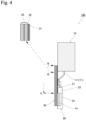
FIG. 4 is a longitudinal cross-sectional view showing a cross section taken along line A-A inFIG. 2 , and the upper left part of the paper in this figure shows an enlarged cross-sectional view of a range between two arrows represented by reference characters B-B; -
FIG. 5 is an exploded perspective view of the connector cable of the first embodiment as viewed from the upper left side of the rear surface; -
FIG. 6 is a perspective view of a connector cable of a second embodiment as viewed from the upper left side of a rear surface; -
FIG. 7 is a top view of the connector cable of the second embodiment; -
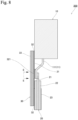
FIG. 8 is a longitudinal cross-sectional view showing a cross section taken along line D-D inFIG. 7 ; -
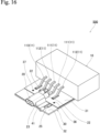
FIG. 9 is a perspective view of a connector cable of a third embodiment as viewed from the upper left side of a rear surface; -
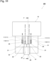
FIG. 10 is a top view of the connector cable of the third embodiment; -
FIG. 11 is a longitudinal cross-sectional view showing a cross section taken along line F-F inFIG. 10 ; -
FIG. 12 is a bottom view of the connector cable of the third embodiment; -
FIG. 13 is a perspective view of a connector cable of a fourth embodiment as viewed from the upper left side of a rear surface; -
FIG. 14 is a top view of the connector cable of the fourth embodiment; -
FIG. 15 is a longitudinal cross-sectional view showing a cross section taken along line G-G inFIG. 14 ; -
FIG. 16 is a perspective view of a connector cable of a fifth embodiment as viewed from the upper left side of a rear surface; -
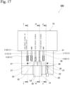
FIG. 17 is a top view of the connector cable of the fifth embodiment; -
FIG. 18 is a longitudinal cross-sectional view showing a cross section taken along line H-H inFIG. 17 ; -
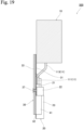
FIG. 19 is a longitudinal cross-sectional view showing a cross section taken along line I-I inFIG. 17 ; -
FIG. 20 is a longitudinal cross-sectional view showing a cross section taken along line J-J inFIG. 17 ; -
FIG. 21 is a perspective view of a connector cable of a sixth embodiment as viewed from the upper left side of a rear surface; -
FIG. 22 is a top view of the connector cable of the sixth embodiment; -
FIG. 23 is a right side view of the connector cable of the sixth embodiment; -
FIG. 24 is a longitudinal cross-sectional view showing a cross section taken along line K-K inFIG. 22 ; -
FIG. 25 is a diagram showing one specific example in various possible examples of the connector cable of the present invention; -
FIG. 26 is a diagram showing another specific example in various possible examples of the connector cable of the present invention; -
FIG. 27 is a perspective view showing an exploded state of a high-speed connector cable according to the invention ofJapanese Patent Laid-Open No. 8-167457 -
FIG. 28 is a perspective view showing a housing and a relay substrate configuring the high-speed connector cable according to the invention ofJapanese Patent Laid-Open No. 8-167457 -
FIG. 29(A) is a front view singly showing a board configuring a relay substrate for a high-speed connector cable according to the invention ofJapanese Patent Laid-Open No. 8-167457 FIG. 29(B) is a cross-sectional view showing a cross section taken along line III-III inFIG. 29A ; and -
FIG. 30 is a perspective view showing a relay substrate and a coaxial cable for a high-speed connector cable according to the invention ofJapanese Patent Laid-Open No. 8-167457 - The following describes suitable embodiments for carrying out the present invention with reference to drawings. Note that: the following embodiments do not limit the invention according to each claim; and not all combinations of characteristics described in the embodiments are essential to the solution of the invention.
- The following describes a first embodiment, which is one possible embodiment of a connector cable of the present invention with reference to
FIGS. 1 to 5 . - As shown in
FIGS. 1 to 5 , aconnector cable 100 of the first embodiment includes aconnector 10, a shieldedcable 20, and arelay substrate 30. Theconnector cable 100 has a configuration in which theconnector 10 and the shieldedcable 20 are connected via therelay substrate 30. - The
connector 10 has a fitting portion (not shown) on a front side, and has aconductive metal contact 11 on a rear side, which is a connection portion. In theconnector 10 of the first embodiment, the fitting portion (not shown) is fitted with a mating connector, and this can make a connection including telecommunications or optical communications between theconnector 10 and the mating connector. Further, theconnector 10 of the first embodiment has fourcontacts 11. As shown inFIG. 2 , in the fourcontacts 11, the twocontacts 111 arranged in the center are used as connection portions for high-speed signals, and twocontacts 112 arranged at both left and right ends are used as connection portions for ground (GND). - The shielded
cable 20 includes aninner conductor 21, a dielectric 22 that covers theinner conductor 21, and ashield member 23 that covers the dielectric 22. Theinner conductor 21 of the first embodiment is used as a conductor for transmitting high-speed signals. The dielectric 22 of the first embodiment is made of an insulating material such as polyethylene, and covers the entire circumference of theinner conductor 21 to protect theinner conductor 21. Theshield member 23 of the first embodiment is a member that further covers the entire circumference of the dielectric 22, and is formed of, for example, a braided wire formed of a braided copper wire or an aluminum strip. Theshield member 23 serves as an electromagnetic shield to protect theinner conductor 21 that transmits high-speed signals, from the influence of electromagnetic waves etc. arriving from the outside. - Note that, in the shielded
cable 20 of the first embodiment shown inFIGS. 1 to 5 , a configuration is illustrated in which twoinner conductors 21 are respectively covered with twodielectrics 22, and the twodielectrics 22 covering theinner conductors 21 are covered with oneshield member 23. However, the form of the shielded cable applicable to the present invention is not limited to that shown inFIGS. 1 to 5 . Examples of shielded cable of the present invention to be used may include: a coaxial cable in which one inner conductor is covered with a dielectric and a shield member; a micro coaxial cable; as well as a high-speed signal cable of a type called STP (shielded twisted pair) cable or SPP (shielded parallel pair) cable. Further, the shielded cable of the present invention includes: a cable having a wire, called a drain wire, built-in over the entire length of the cable; and a cable having no built-in wire. - As shown in
FIG. 4 , on the bottom surface part of therelay substrate 30, there is formed asubstrate layer 33 having two substrates attached therein, and on the front surface of thesubstrate layer 33, there is formed aGND conductor layer 32. Further, on the upper surface of theGND conductor layer 32, which is formed on the front surface of thesubstrate layer 33, there is formed an insulatingmember 31 made of an insulating material. - For the
substrate layer 33 of the first embodiment, any conventionally known substrate material can be used. The substrate material includes, for example, a material using a phenol resin-based resin material, an epoxy resin-based resin material, a glass non-woven fabric impregnated with an epoxy resin, and an aluminum-based plate material. Further, the insulatingmember 31 of the first embodiment to be used includes a resist coated to the front surface of theGND conductor layer 32. The resist, which is the insulatingmember 31 of the first embodiment, is a coating material also called a solder resist. The resist demonstrates a function to prevent solder from adhering to unnecessary parts during soldering, and at the same time, protect therelay substrate 30 from dust, heat, moisture, etc. as a permanent protective film to maintain insulation. - The
connector cable 100 of the first embodiment includes the above-describedconnector 10, the shieldedcable 20, and therelay substrate 30. Theconnector 10 and the shieldedcable 20 are connected via therelay substrate 30. Then, in theconnector cable 100 of the first embodiment, as shown inFIGS. 1 to 4 , theshield member 23 and the dielectric 22 of the shieldedcable 20 are removed to expose theinner conductor 21. With this state, the exposedinner conductor 21 is directly connected to thecontact 111 for high-speed signals of theconnector 10. Here, the connection between theinner conductor 21 and thecontact 111 for high-speed signals uses soldering. Thus directly connecting theinner conductor 21 and thecontact 111 for high-speed signals can significantly reduce the substrate wiring loss as compared with the conventional connection via the substrate. - Further, as shown in
FIG. 5 , theGND contact 112 provided in theconnector 10 can be connected to theGND conductor layer 32 by means of: providing a GND conductor layer exposedportion 34, where no insulatingmember 31 made of a resist is coated, in a part of theGND conductor layer 32 on the front surface of therelay substrate 30; and placing theGND contact 112 at the position of the GND conductor layer exposedportion 34 and soldering it there. - As shown in
FIG. 4 , the first embodiment has a configuration such that: theGND conductor layer 32 on the front surface of therelay substrate 30 is arranged directly under a position where theshield member 23 is removed to expose the dielectric 22; and theGND conductor layer 32 on the front surface of therelay substrate 30, arranged directly under the part where theshield member 23 is removed, is covered with the insulatingmember 31 made of a resist. Further, as shown inFIG. 4 , the first embodiment has a configuration such that: theGND conductor layer 32 on the front surface of therelay substrate 30 extends to a position directly under thecontact 111 for high-speed signals of theconnector 10 and the exposedinner conductor 21 of the shieldedcable 20; and theGND conductor layer 32 on the front surface of therelay substrate 30, which extends to the positions directly under thecontact 111 for high-speed signals of theconnector 10 and the exposedinner conductor 21 of the shieldedcable 20, is also covered with the insulatingmember 31 made of a resist. - Further, as shown in
FIG. 4 , the first embodiment has a configuration such that: theGND conductor layer 32 on the front surface of therelay substrate 30 is exposed at the position directly under theshield member 23 of the shieldedcable 20. With this state, theGND conductor layer 32 is not covered with the insulatingmember 31 made of a resist. Then theshield member 23 of the shieldedcable 20 and theGND conductor layer 32 on the front surface of therelay substrate 30 are fixedly connected by thesolder 41. - The following describes the detailed structure of the
connector cable 100 of the first embodiment with reference toFIG. 4 . Thus soldering theshield member 23 of the shieldedcable 20 to theGND conductor layer 32 on the front surface of therelay substrate 30 brings about effects such as noise prevention. In other words, theGND conductor layer 32 on the front surface of therelay substrate 30 is arranged at a position directly under theshield member 23 in a state in which theGND conductor layer 32 is not covered with the insulatingmember 31 made of a resist. - On the other hand, at the part where the
shield member 23 of the shieldedcable 20 is removed and the dielectric 22 is exposed, the impedance increases because the dielectric 22 has no covering. The countermeasure is arranging theGND conductor layer 32 on the front surface of therelay substrate 30 in a state of being covered with an insulatingmember 31 made of a resist at a position directly under the exposeddielectric 22, to obtain the effect of lowering impedance. - In other words, the
GND conductor layer 32 on the front surface of therelay substrate 30 has a boundary at a position indicated by reference character C inFIG. 4 . The one side of the boundary, where theconnector 10 is arranged, is coated with an insulatingmember 31 made of a resist, and the other side thereof, where theshield member 23 of the shieldedcable 20 is located, is not coated with an insulatingmember 31 made of a resist. This countermeasure achieves impedance matching in theconnector cable 100 of the first embodiment. - In other words, the
connector cable 100 of the first embodiment has the insulatingmember 31 and theGND conductor layer 32 on the front surface of therelay substrate 30, directly under the part where theshield member 23 of the shieldedcable 20 has been removed. This effectively prevents increase in impedance. Additionally, in theconnector cable 100 of the first embodiment, thecontact 111 for high-speed signals of theconnector 10 and theinner conductor 21 of the shieldedcable 20 are connected directly by soldering. This eliminates, for example, need for process of bending (forming) theinner conductor 21 to the front surface of the substrate. Further,GND conductor layer 32 on the front surface of therelay substrate 30, arranged directly under the part where theshield member 23 is removed, is not adjacent to theinner conductor 21 of the shieldedcable 20. Specifically, theGND conductor layer 32 is separated from the inner conductor 24 in the vertical direction, and the insulatingmember 31 is interposed between the two members. As a result, there is no short circuit. Thus, theconnector cable 100 of the first embodiment can bring the effects described above. From the above, according to theconnector cable 100 of the first embodiment, there can be provided a connector cable that prevents both increase in impedance and a short circuit. - The above has described the first embodiment, which is one possible embodiment of the connector cable of the present invention, with reference to
FIGS. 1 to 5 . However, the technical scope of the present invention is not limited to the scope described in the first embodiment. Various modifications or improvements can be made to the first embodiment. Then, the following describes various possible embodiments of the connector cable of the present invention. In each of the embodiments described below, the same or similar members as those in the above-described first embodiment are designated by the same reference numerals and characters, and the description thereof is to be omitted. - The following describes a
connector cable 200 of a second embodiment with reference toFIGS. 6 to 8 . - In the
connector cable 200 of the second embodiment, the connection part between thecontact 111 for high-speed signals of theconnector 10 and the exposedinner conductor 21 of the shieldedcable 20 is connected by soldering, as in the case of the first embodiment described above. Additionally, as shown in more detail inFIG. 8 , theconnector cable 200 of the second embodiment has theGND conductor layer 32 on the front surface of therelay substrate 30. TheGND conductor layer 32 located directly under the connection part between thecontact 111 for high-speed signals and theinner conductor 21 is cut out in the range of arrow indicated by reference character E inFIG. 8 . Thus, theconnector cable 200 has a structural feature in which there is formed a GND cut-outregion 321 where theGND conductor layer 32 is absent. - Here, the connection part between the
contact 111 for high-speed signals and theinner conductor 21 is connected by soldering, so that a problem arises in which the impedance decreases only at this part. To solve this problem, in the second embodiment, theGND conductor layer 32 on the front surface of therelay substrate 30 is cut out directly under the connection part between thecontact 111 for high-speed signals and theinner conductor 21. This forms a GND cut-outregion 321 where theGND conductor layer 32 is absent, to increase the impedance. As a result, the second embodiment can achieve impedance matching of theconnector cable 200 as a whole. In other words, according to theconnector cable 200 of the second embodiment, there can be provided a connector cable that prevents both increase in impedance and a short circuit, and achieves more suitable impedance matching. - The following describes a
connector cable 300 of a third embodiment with reference toFIGS. 9 to 12 . - In the
connector cable 300 of the third embodiment, the connection part between thecontact 111 for high-speed signals of theconnector 10 and the exposedinner conductor 21 of the shieldedcable 20 is connected by soldering, as in the case of the first embodiment described above. Additionally, in theconnector cable 300 of the third embodiment, therelay substrate 30 itself located directly under the connection part between thecontact 111 for high-speed signals and theinner conductor 21 is cut out, as shown inFIGS. 9 to 12 . Thus, theconnector cable 300 has a structural feature in which there is formed a substrate cut-outregion 35 where therelay substrate 30 itself is absent. - Here, the connection part between the
contact 111 for high-speed signals and theinner conductor 21 is connected by soldering, so that a problem arises in which the impedance decreases only at this part. To solve this problem, therelay substrate 30 itself is cut out directly under the connection part between thecontact 111 for high-speed signals and theinner conductor 21 in the third embodiment. This forms a substrate cut-outregion 35 where the substrate including theGND conductor layer 32 is absent to increase the impedance. As a result, the third embodiment can achieve the impedance matching of theconnector cable 300 as a whole. In other words, according to theconnector cable 300 of the third embodiment, there can be provided a connector cable that prevents both increase in impedance and a short circuit, and achieves more suitable impedance matching, as in the second embodiment described above. - The following describes a
connector cable 400 of a fourth embodiment with reference toFIGS. 13 to 15 . - In the
connector cable 400 of the fourth embodiment, the connection part between thecontact 111 for high-speed signals of theconnector 10 and the exposedinner conductor 21 of the shieldedcable 20 is connected by soldering, as in the case of the first embodiment described above. Additionally, in theconnector cable 400 of a fourth embodiment, theconnector mold 14 that configures theconnector 10 by installation of thecontact 11 includes acontact 11 of theconnector 10 and a connectormold extension portion 15 extending to directly under the connection part, as shown inFIGS. 13-15 . - Then, the connection part between the
contact 111 for high-speed signals and theinner conductor 21 is connected by soldering, so that a problem arises in which the impedance decreases only at this part. To solve this problem, in the fourth embodiment, a connectormold extension portion 15, which is a part of theconnector mold 14, is formed up to a position directly under the connection part between thecontact 111 for high-speed signals and theinner conductor 21. This forms a region where the substrate including theGND conductor layer 32 is absent, to increase the impedance. As a result, the fourth embodiment can achieve the impedance matching of theconnector cable 400 as a whole. In other words, according to theconnector cable 400 of the fourth embodiment, there can be provided a connector cable that prevents both increase in impedance and a short circuit, and achieves more suitable impedance matching, as in the case of the second and third embodiments described above. - Therefore, the
connector cable 200 of the second embodiment, theconnector cable 300 of the third embodiment, and theconnector cable 400 of the fourth embodiment can have the advantage of preventing local impedance reduction and providing more suitable impedance matching. - The following describes a
connector cable 500 of a fifth embodiment with reference toFIGS. 16 to 20 . - The
connector cable 500 of the fifth embodiment shows a configuration example in which types of thecontact 11 of theconnector 10 are various, and a plurality of types of thecontact 11 are mixed as compared to the case of the first embodiment described above. - Specifically, the
connector 10 of the fifth embodiment has fivecontacts 11 installed therein. As shown inFIG. 17 , the fivecontacts 11 include onecontact 112 for one GND (ground), twocontacts 111 for high-speed signals, onecontact 112 for one GND (ground), and onecontact 113 for the power supply (or for low-speed signals), which are arranged in this order from the left end to the right end. - On the other hand, the shielded
cable 20 is installed in the same arrangement as in the first to third embodiments described above, which achieves appropriate impedance matching. However, theconnector cable 500 of the fifth embodiment includesunshielded cables 25 such as cables for power supply or cables for low-speed signals. Therefore, it is necessary to connect theunshielded cable 25 to thecontact 113 for power supply (or for low-speed signals). However, the specifications and usage conditions of theconnector cable 500 may arrange theunshielded cable 25 and thecontact 113 for power supply (or for low-speed signals) at separate positions, as shown inFIG. 17 etc. - A countermeasure for this case in the
connector cable 500 of the fifth embodiment is forming twovias relay substrate 30, and providing a substrateinner conductor 38 connecting these twovias relay substrate 30. Such a configuration allows theunshielded cable 25 to connect to thecontact 113 for power supply (or low-speed signals) of theconnector 10 via the substrateinner conductor 38 provided inside therelay substrate 30. In other words, theconnector cable 500 of the fifth embodiment does not disturb the impedance matched connection between thecontact 111 for high-speed signals and the exposedinner conductor 21 of the shieldedcable 20, and can connect anunshielded cable 25 to thecontact 113 for power supply (or for low-speed signals) of theconnector 10. Therefore, according to the fifth embodiment, there can be provided aconnector cable 500 in which cable routing is easy. - Note that the
vias inner conductor 38 of the fifth embodiment configures the conductor of the present invention provided inside therelay substrate 30. In addition, thevias - The following describes a
connector cable 600 of a sixth embodiment with reference toFIGS. 21 to 24 . - The
connector cable 600 of the sixth embodiment shown inFIGS. 21 to 24 is configured such that: there are prepared twoconnector cables 100 of the first embodiment described above; the twoconnector cables 100 are attached to each other at their bottom surfaces of therelay substrates 30; and theconnector cable 100 on the back surface side and theconnector cable 100 on the front surface side are arranged so as to be mirror image symmetric. - In other words, the
connector cable 600 of the sixth embodiment is configured such that: therelay substrate 30 also has theGND conductor layer 32 provided on the back surface side; and thecontact 11 of theconnector 10, the shieldedcable 20, and theGND conductor layer 32 are arranged on the back surface side and the front surface side so as to be mirror image symmetric. Also according to theconnector cable 600 of the sixth embodiment having such an arrangement configuration, there can be provided a connector cable that prevent both increase in impedance and a short circuit. - With reference to
FIGS. 1 to 24 , the above has described various possible embodiments of the present invention including theconnector cables FIGS. 25 and26 . Note that various electronic components may be mounted on the relay substrate of the present invention, and in such a case, the unshielded cable and the contact may be connected via the various electronic components. - The example shown in
FIG. 25 is an example in which theconnector cable 200 of the second embodiment and theconnector cable 500 of the fifth embodiment are combined. The connector cable of this example allows easy cable routing if types ofcontacts 11 of theconnector 10 are various and a plurality of types ofcontacts 11 are mixed. This can make the connector cable highly expandable. In addition, direct connection of theinner conductor 21 of the shieldedcable 20 to thecontact 111 for high-speed signals of theconnector 10 can reduce transmission loss on therelay substrate 30. At the same time, making therelay substrate 30 smaller in the depth direction can bring about an effect of expanding the applicable range and reducing the cost. - The example shown in
FIG. 26 is an example in which theconnector cable 300 of the third embodiment and theconnector cable 500 of the fifth embodiment are combined. The connector cable of this example can obtain the same effect as that of the example shown inFIG. 25 . Additionally, if thecontact 11 of theconnector 10 is displaced in the vertical direction, for example, the substrate cut-outregion 35 facilitates correcting the position of thecontact 111 for high-speed signals and theinner conductor 21, which leads to an advantage of high degree of freedom in connection. Further, adjusting the shape of thecontact 111 for high-speed signals and the substrate cut-outregion 35 can adjust impedance matching. - The present invention relates to a connector cable in which a connector and a shielded cable are connected via a relay substrate, and is particularly useful for connector cables that transmit high-speed signals.
-
- 100
- connector cable (of the first embodiment)
- 200
- connector cable (of the second embodiment)
- 300
- connector cable (of the third embodiment)
- 400
- connector cable (of the fourth embodiment)
- 500
- connector cable (of the fifth embodiment)
- 600
- connector cable (of the sixth embodiment)
- 10
- connector
- 11
- contact
- 14
- connector mold
- 15
- connector mold extension portion
- 111
- contact for high-speed signals
- 112
- contact for GND
- 113
- contact for power supply (or for low-speed signals)
- 20
- shielded cable
- 21
- inner conductor
- 22
- dielectric
- 23
- shield member
- 25
- unshielded cable
- 30
- relay substrate
- 31
- insulating member
- 32
- GND conductor layer
- 321
- GND cut-out region
- 33
- substrate layer
- 34
- GND conductor layer exposed portion
- 35
- substrate cut-out region
- 36, 37
- via (conductor)
- 38
- substrate inner conductor (conductor)
- 41
- solder
- THE FOLLOWING ASPECTS ARE PREFERRED EMBODIMENTS OF THE INVENTION
- 1. A connector cable comprising:
- a connector;
- a shielded cable; and
- a relay substrate, the connector and the shielded cable being connected via the relay substrate,
- wherein: the shielded cable includes at least an inner conductor, a dielectric covering the inner conductor, and a shield member covering the dielectric;
- the inner conductor is connected to a contact of the connector at a part where the shield member and the dielectric are removed to expose the inner conductor;
- at least directly under a part where the shield member is removed to expose the dielectric, a ground (GND) conductor layer on a front surface of the relay substrate is arranged; and
- the GND conductor layer on the front surface of the relay substrate, which is arranged directly under the part where the shield member is removed, is covered with an insulating member.
- 2. The connector cable according to aspect 1, wherein
the insulating member is a resist coated to the front surface of the GND conductor layer. - 3. The connector cable according to
aspect 1 or 2, wherein- a connection part between the contact of the connector and the exposed inner conductor of the shielded cable is connected by soldering,
- the GND conductor layer on the front surface of the relay substrate is extended to directly under the contact of the connector and the connection part, and
- the GND conductor layer directly under the connection part is cut out.
- 4. The connector cable according to
aspect 1 or 2, wherein- the connection part between the contact of the connector and the exposed inner conductor of the shielded cable is connected by soldering, and
- the relay substrate is cut out at a part directly under the contact of the connector and the exposed inner conductor of the shielded cable.
- 5. The connector cable according to
aspect 1 or 2, wherein- the contact of the connector is held in an insulation connector mold,
- the connection part between the contact of the connector and the exposed inner conductor of the shielded cable is connected by soldering, and
- the connector mold extends to directly under the contact of the connector and the connection part.
- 6. The connector cable according to any one of aspects 1 to 5, wherein
- one or more unshielded cables are connected to the connector, and
- at least one of the unshielded cables is connected to the contact of the connector via a conductor of the relay substrate.
- 7. The connector cable according to any one of aspects 1 to 6, wherein
- the relay substrate also has a GND conductor layer on a back surface side, and
- the contact of the connector, the shielded cable, and the GND conductor layer are arranged so as to be mirror image symmetric with the front surface side.
Claims (5)
- A connector cable (300, 500, 600) comprising:a connector (10);a shielded cable (20); anda relay substrate (30), the connector (10) and the shielded cable (20) being connected via the relay substrate (30),wherein: the shielded cable (20) includes at least an inner conductor (21), a dielectric (22) covering the inner conductor (21), and a shield member (23) covering the dielectric (22);the inner conductor (21) is connected to a contact (11) of the connector (10) at a part where the shield member (23) and the dielectric (22) are removed to expose the inner conductor (21);at least directly under a part where the shield member (23) is removed to expose the dielectric (22), a ground conductor layer (32) on a front surface of the relay substrate (30) is arranged; andthe ground conductor layer (32) on the front surface of the relay substrate (30), which is arranged directly under the part where the shield member (23) is removed, is covered with an insulating member (31),wherein the connection part between the contact (11) of the connector (10) and the exposed inner conductor (21) of the shielded cable (20) is connected by soldering, andthe relay substrate (30) is cut out at a part directly under the contact (11) of the connector (10) and the exposed inner conductor (21) of the shielded cable (20) for forming a cut-out region where the relay substrate (30) including the ground conductor layer (32) is absent.
- A connector cable (400, 500, 600) comprising:a connector (10);a shielded cable (20); anda relay substrate (30), the connector (10) and the shielded cable (20) being connected via the relay substrate (30),wherein: the shielded cable (20) includes at least an inner conductor (21), a dielectric (22) covering the inner conductor (21), and a shield member (23) covering the dielectric (22);the inner conductor (21) is connected to a contact (11) of the connector (10) at a part where the shield member (23) and the dielectric (22) are removed to expose the inner conductor (21);at least directly under a part where the shield member (23) is removed to expose the dielectric (22), a ground conductor layer (32) on a front surface of the relay substrate (30) is arranged; andthe ground conductor layer (32) on the front surface of the relay substrate (30), which is arranged directly under the part where the shield member (23) is removed, is covered with an insulating member (31),wherein the contact (11) of the connector (10) is held in an insulation connector mold (14),the connection part between the contact (11) of the connector (10) and the exposed inner conductor (21) of the shielded cable (20) is connected by soldering, andthe connector mold (14) extends to directly under the contact (11) of the connector (10) and the connection part for forming a region where the relay substrate (30) including the ground conductor layer (32) is absent.
- The connector cable (300, 400, 500, 600) according to claim 1, wherein
the insulating member (31) is a resist coated to the front surface of the GND conductor layer (32). - The connector cable (500) according to any one of claims 1 to 5, whereinone or more unshielded cables (25) are connected to the connector (10), andat least one of the unshielded cables (25) is connected to the contact (11) of the connector (10) via a conductor (36, 37) of the relay substrate (30).
- The connector cable (500) according to any one of claims 1 to 6, whereinthe relay substrate (30) also has a ground conductor layer (32) on a back surface side, andthe contact (11) of the connector (10), the shielded cable (20), and the ground conductor layer (32) are arranged so as to be mirror image symmetric with the front surface side.
Applications Claiming Priority (2)
| Application Number | Priority Date | Filing Date | Title |
|---|---|---|---|
| JP2021081890A JP7608265B2 (en) | 2021-05-13 | 2021-05-13 | Connectors and Cables |
| EP22164574.0A EP4089842B1 (en) | 2021-05-13 | 2022-03-25 | Connector cable |
Related Parent Applications (2)
| Application Number | Title | Priority Date | Filing Date |
|---|---|---|---|
| EP22164574.0A Division EP4089842B1 (en) | 2021-05-13 | 2022-03-25 | Connector cable |
| EP22164574.0A Division-Into EP4089842B1 (en) | 2021-05-13 | 2022-03-25 | Connector cable |
Publications (3)
| Publication Number | Publication Date |
|---|---|
| EP4398685A2 true EP4398685A2 (en) | 2024-07-10 |
| EP4398685A3 EP4398685A3 (en) | 2024-09-11 |
| EP4398685B1 EP4398685B1 (en) | 2025-05-21 |
Family
ID=80952175
Family Applications (2)
| Application Number | Title | Priority Date | Filing Date |
|---|---|---|---|
| EP22164574.0A Active EP4089842B1 (en) | 2021-05-13 | 2022-03-25 | Connector cable |
| EP24171954.1A Active EP4398685B1 (en) | 2021-05-13 | 2022-03-25 | Connector cable |
Family Applications Before (1)
| Application Number | Title | Priority Date | Filing Date |
|---|---|---|---|
| EP22164574.0A Active EP4089842B1 (en) | 2021-05-13 | 2022-03-25 | Connector cable |
Country Status (6)
| Country | Link |
|---|---|
| US (1) | US11978993B2 (en) |
| EP (2) | EP4089842B1 (en) |
| JP (1) | JP7608265B2 (en) |
| CN (1) | CN115347421B (en) |
| ES (2) | ES2982899T3 (en) |
| TW (1) | TWI806435B (en) |
Families Citing this family (7)
| Publication number | Priority date | Publication date | Assignee | Title |
|---|---|---|---|---|
| JP2023107606A (en) | 2022-01-24 | 2023-08-03 | 日本航空電子工業株式会社 | Connector/Cable |
| US12476398B2 (en) | 2022-08-02 | 2025-11-18 | Te Connectivity Solutions Gmbh | Cable assembly for a cable connector module |
| US12489231B2 (en) | 2022-08-02 | 2025-12-02 | Te Connectivity Solutions Gmbh | Cable assembly for a cable connector module |
| US12482969B2 (en) | 2022-08-02 | 2025-11-25 | Te Connectivity Solutions Gmbh Et Al. | Cable assembly for a cable connector module |
| US11924970B2 (en) * | 2022-08-02 | 2024-03-05 | Te Connectivity Solutions Gmbh | Cable assembly for a cable connector module |
| US12388205B2 (en) | 2022-08-02 | 2025-08-12 | Te Connectivity Solutions Gmbh | Electronic assembly having a cable connector module |
| JP7857541B2 (en) * | 2022-12-26 | 2026-05-13 | 株式会社オートネットワーク技術研究所 | Connection structure between electric wire and circuit board, and temperature measuring unit |
Citations (1)
| Publication number | Priority date | Publication date | Assignee | Title |
|---|---|---|---|---|
| JPH08167457A (en) | 1994-12-15 | 1996-06-25 | Kel Corp | Electrical connector |
Family Cites Families (20)
| Publication number | Priority date | Publication date | Assignee | Title |
|---|---|---|---|---|
| JPS61161763U (en) * | 1985-03-29 | 1986-10-07 | ||
| JP2003045577A (en) * | 2001-08-03 | 2003-02-14 | Smk Corp | Connector cable |
| WO2007004773A1 (en) * | 2005-06-30 | 2007-01-11 | Yoowon Com-Tech Co., Ltd | Connecting structure of printed circuit board including patterned grounding contact |
| JP2009123500A (en) * | 2007-11-14 | 2009-06-04 | Hosiden Corp | Base board assembly |
| US7651379B1 (en) * | 2008-10-23 | 2010-01-26 | Hon Hai Precision Ind. Co., Ltd | Cable assembly with improved termination disposition |
| EP2519086B1 (en) * | 2011-04-26 | 2016-03-23 | Tyco Electronics Belgium EC BVBA | High speed input/output connection interface element, cable assembly and interconnection system with reduced cross-talk |
| JP2013114999A (en) | 2011-11-30 | 2013-06-10 | Sumitomo Electric Ind Ltd | Cable module and method of manufacturing the same |
| US9356400B2 (en) * | 2013-07-19 | 2016-05-31 | Foxconn Interconnect Technology Limited | Flippable electrical connector |
| US10109937B2 (en) * | 2013-10-25 | 2018-10-23 | Fci Usa Llc | Electrical cable connector |
| CN106105407A (en) * | 2014-03-20 | 2016-11-09 | 奥林巴斯株式会社 | Cable connecting structure and endoscope apparatus |
| US20160218455A1 (en) * | 2015-01-26 | 2016-07-28 | Samtec, Inc. | Hybrid electrical connector for high-frequency signals |
| US9401573B1 (en) * | 2015-12-29 | 2016-07-26 | Xentris Wireless Llc | Electrical plug connector |
| CN106998016B (en) * | 2016-01-25 | 2021-05-25 | 富士康(昆山)电脑接插件有限公司 | Cable assembly with improved cable retention |
| JP6132963B2 (en) * | 2016-06-01 | 2017-05-24 | オリンパス株式会社 | Cable connection structure, ultrasound probe and ultrasound endoscope system |
| CN109565122B (en) | 2016-08-18 | 2021-03-02 | 申泰公司 | Direct-attach connector |
| JP6801306B2 (en) * | 2016-08-31 | 2020-12-16 | 住友電気工業株式会社 | Shielded flat cable |
| US20170221604A1 (en) | 2017-04-14 | 2017-08-03 | Apple Inc. | Ground bar for micro-coaxial wires in hdmi cables |
| CN109149279B (en) * | 2017-06-16 | 2024-07-16 | 泰科电子(上海)有限公司 | Connector components |
| US11410790B2 (en) * | 2018-04-27 | 2022-08-09 | Sumitomo Electric Industries, Ltd. | Substrate-mounted electrical connector for connecting to a shielded flat cable |
| CN119297666A (en) * | 2019-07-01 | 2025-01-10 | 安费诺富加宜(亚洲)私人有限公司 | Wire-to-board connector with low profile |
-
2021
- 2021-05-13 JP JP2021081890A patent/JP7608265B2/en active Active
-
2022
- 2022-01-19 CN CN202210063252.3A patent/CN115347421B/en active Active
- 2022-02-10 US US17/668,518 patent/US11978993B2/en active Active
- 2022-02-18 TW TW111105949A patent/TWI806435B/en active
- 2022-03-25 EP EP22164574.0A patent/EP4089842B1/en active Active
- 2022-03-25 EP EP24171954.1A patent/EP4398685B1/en active Active
- 2022-03-25 ES ES22164574T patent/ES2982899T3/en active Active
- 2022-03-25 ES ES24171954T patent/ES3033911T3/en active Active
Patent Citations (1)
| Publication number | Priority date | Publication date | Assignee | Title |
|---|---|---|---|---|
| JPH08167457A (en) | 1994-12-15 | 1996-06-25 | Kel Corp | Electrical connector |
Also Published As
| Publication number | Publication date |
|---|---|
| EP4398685B1 (en) | 2025-05-21 |
| US11978993B2 (en) | 2024-05-07 |
| CN115347421A (en) | 2022-11-15 |
| EP4398685A3 (en) | 2024-09-11 |
| JP7608265B2 (en) | 2025-01-06 |
| ES3033911T3 (en) | 2025-08-11 |
| EP4089842A1 (en) | 2022-11-16 |
| US20220368041A1 (en) | 2022-11-17 |
| ES2982899T3 (en) | 2024-10-18 |
| EP4089842B1 (en) | 2024-05-29 |
| TW202245356A (en) | 2022-11-16 |
| TWI806435B (en) | 2023-06-21 |
| JP2022175488A (en) | 2022-11-25 |
| CN115347421B (en) | 2026-01-16 |
Similar Documents
| Publication | Publication Date | Title |
|---|---|---|
| EP4398685B1 (en) | Connector cable | |
| EP2519086B1 (en) | High speed input/output connection interface element, cable assembly and interconnection system with reduced cross-talk | |
| US10069258B2 (en) | Crosstail-shaped conductive spacer extending rearwardly from a printed circuit board | |
| US7204722B2 (en) | Communications jack with compensation for differential to differential and differential to common mode crosstalk | |
| CA2313679C (en) | Electrical connector system with cross-talk compensation | |
| US7677927B2 (en) | High bandwidth connector | |
| US10178762B2 (en) | Device and method for transmitting differential data signals | |
| EP4195426A1 (en) | Communications plugs having capacitors that inject offending crosstalk after a plug-jack mating point and related connectors and methods | |
| EP4099510A1 (en) | Multiple coaxial connector | |
| KR100418452B1 (en) | High frequency signal switching unit | |
| KR100421434B1 (en) | Electrical connector with enhanced grounding characteristics | |
| US20240322497A1 (en) | Connector Assembly Including Receptacle Connector and Plug Connector, and Plug Connector | |
| US7382214B2 (en) | Printed board | |
| US6971896B2 (en) | Flex strips for high frequency connectors | |
| WO2023199827A1 (en) | Cable assembly and connector | |
| FI90935C (en) | Method of installing a coaxial transmission line on a printed circuit board | |
| JP2014067561A (en) | Optical module | |
| JP4421243B2 (en) | Combined structure consisting of chassis and printed circuit board | |
| JPH07111468A (en) | High frequency separator between multiple metal enclosures | |
| KR19990000169A (en) | Flexible PC Cable for Backboard Connection |
Legal Events
| Date | Code | Title | Description |
|---|---|---|---|
| PUAI | Public reference made under article 153(3) epc to a published international application that has entered the european phase |
Free format text: ORIGINAL CODE: 0009012 |
|
| STAA | Information on the status of an ep patent application or granted ep patent |
Free format text: STATUS: THE APPLICATION HAS BEEN PUBLISHED |
|
| AC | Divisional application: reference to earlier application |
Ref document number: 4089842 Country of ref document: EP Kind code of ref document: P |
|
| AK | Designated contracting states |
Kind code of ref document: A2 Designated state(s): AL AT BE BG CH CY CZ DE DK EE ES FI FR GB GR HR HU IE IS IT LI LT LU LV MC MK MT NL NO PL PT RO RS SE SI SK SM TR |
|
| REG | Reference to a national code |
Ref country code: DE Ref legal event code: R079 Free format text: PREVIOUS MAIN CLASS: H05K0003340000 Ipc: H01R0009050000 Ref country code: DE Ref legal event code: R079 Ref document number: 602022015092 Country of ref document: DE Free format text: PREVIOUS MAIN CLASS: H05K0003340000 Ipc: H01R0009050000 |
|
| PUAL | Search report despatched |
Free format text: ORIGINAL CODE: 0009013 |
|
| AK | Designated contracting states |
Kind code of ref document: A3 Designated state(s): AL AT BE BG CH CY CZ DE DK EE ES FI FR GB GR HR HU IE IS IT LI LT LU LV MC MK MT NL NO PL PT RO RS SE SI SK SM TR |
|
| RIC1 | Information provided on ipc code assigned before grant |
Ipc: H05K 3/34 20060101ALN20240805BHEP Ipc: H05K 1/11 20060101ALI20240805BHEP Ipc: H01R 13/6594 20110101ALI20240805BHEP Ipc: H01R 12/53 20110101ALI20240805BHEP Ipc: H01R 9/05 20060101AFI20240805BHEP |
|
| RAP3 | Party data changed (applicant data changed or rights of an application transferred) |
Owner name: JAPAN AVIATION ELECTRONICS INDUSTRY, LIMITED |
|
| STAA | Information on the status of an ep patent application or granted ep patent |
Free format text: STATUS: REQUEST FOR EXAMINATION WAS MADE |
|
| 17P | Request for examination filed |
Effective date: 20241205 |
|
| GRAP | Despatch of communication of intention to grant a patent |
Free format text: ORIGINAL CODE: EPIDOSNIGR1 |
|
| STAA | Information on the status of an ep patent application or granted ep patent |
Free format text: STATUS: GRANT OF PATENT IS INTENDED |
|
| RIC1 | Information provided on ipc code assigned before grant |
Ipc: H05K 3/34 20060101ALN20250212BHEP Ipc: H05K 1/11 20060101ALI20250212BHEP Ipc: H01R 13/6594 20110101ALI20250212BHEP Ipc: H01R 12/53 20110101ALI20250212BHEP Ipc: H01R 9/05 20060101AFI20250212BHEP |
|
| INTG | Intention to grant announced |
Effective date: 20250226 |
|
| GRAS | Grant fee paid |
Free format text: ORIGINAL CODE: EPIDOSNIGR3 |
|
| GRAA | (expected) grant |
Free format text: ORIGINAL CODE: 0009210 |
|
| STAA | Information on the status of an ep patent application or granted ep patent |
Free format text: STATUS: THE PATENT HAS BEEN GRANTED |
|
| RIN1 | Information on inventor provided before grant (corrected) |
Inventor name: NEMOTO, TAKASHI Inventor name: TANAKA, YUKITAKA Inventor name: KUROKI, YOSHIHIDE Inventor name: KIUCHI, HIDEKI |
|
| AC | Divisional application: reference to earlier application |
Ref document number: 4089842 Country of ref document: EP Kind code of ref document: P |
|
| AK | Designated contracting states |
Kind code of ref document: B1 Designated state(s): AL AT BE BG CH CY CZ DE DK EE ES FI FR GB GR HR HU IE IS IT LI LT LU LV MC MK MT NL NO PL PT RO RS SE SI SK SM TR |
|
| REG | Reference to a national code |
Ref country code: GB Ref legal event code: FG4D |
|
| REG | Reference to a national code |
Ref country code: CH Ref legal event code: EP |
|
| REG | Reference to a national code |
Ref country code: DE Ref legal event code: R096 Ref document number: 602022015092 Country of ref document: DE |
|
| REG | Reference to a national code |
Ref country code: IE Ref legal event code: FG4D |
|
| REG | Reference to a national code |
Ref country code: ES Ref legal event code: FG2A Ref document number: 3033911 Country of ref document: ES Kind code of ref document: T3 Effective date: 20250811 |
|
| REG | Reference to a national code |
Ref country code: NL Ref legal event code: MP Effective date: 20250521 |
|
| PG25 | Lapsed in a contracting state [announced via postgrant information from national office to epo] |
Ref country code: FI Free format text: LAPSE BECAUSE OF FAILURE TO SUBMIT A TRANSLATION OF THE DESCRIPTION OR TO PAY THE FEE WITHIN THE PRESCRIBED TIME-LIMIT Effective date: 20250521 Ref country code: PT Free format text: LAPSE BECAUSE OF FAILURE TO SUBMIT A TRANSLATION OF THE DESCRIPTION OR TO PAY THE FEE WITHIN THE PRESCRIBED TIME-LIMIT Effective date: 20250922 |
|
| REG | Reference to a national code |
Ref country code: LT Ref legal event code: MG9D |
|
| PG25 | Lapsed in a contracting state [announced via postgrant information from national office to epo] |
Ref country code: NO Free format text: LAPSE BECAUSE OF FAILURE TO SUBMIT A TRANSLATION OF THE DESCRIPTION OR TO PAY THE FEE WITHIN THE PRESCRIBED TIME-LIMIT Effective date: 20250821 Ref country code: GR Free format text: LAPSE BECAUSE OF FAILURE TO SUBMIT A TRANSLATION OF THE DESCRIPTION OR TO PAY THE FEE WITHIN THE PRESCRIBED TIME-LIMIT Effective date: 20250822 |
|
| PG25 | Lapsed in a contracting state [announced via postgrant information from national office to epo] |
Ref country code: NL Free format text: LAPSE BECAUSE OF FAILURE TO SUBMIT A TRANSLATION OF THE DESCRIPTION OR TO PAY THE FEE WITHIN THE PRESCRIBED TIME-LIMIT Effective date: 20250521 Ref country code: PL Free format text: LAPSE BECAUSE OF FAILURE TO SUBMIT A TRANSLATION OF THE DESCRIPTION OR TO PAY THE FEE WITHIN THE PRESCRIBED TIME-LIMIT Effective date: 20250521 |
|
| PG25 | Lapsed in a contracting state [announced via postgrant information from national office to epo] |
Ref country code: BG Free format text: LAPSE BECAUSE OF FAILURE TO SUBMIT A TRANSLATION OF THE DESCRIPTION OR TO PAY THE FEE WITHIN THE PRESCRIBED TIME-LIMIT Effective date: 20250521 |
|
| PG25 | Lapsed in a contracting state [announced via postgrant information from national office to epo] |
Ref country code: HR Free format text: LAPSE BECAUSE OF FAILURE TO SUBMIT A TRANSLATION OF THE DESCRIPTION OR TO PAY THE FEE WITHIN THE PRESCRIBED TIME-LIMIT Effective date: 20250521 |
|
| PG25 | Lapsed in a contracting state [announced via postgrant information from national office to epo] |
Ref country code: RS Free format text: LAPSE BECAUSE OF FAILURE TO SUBMIT A TRANSLATION OF THE DESCRIPTION OR TO PAY THE FEE WITHIN THE PRESCRIBED TIME-LIMIT Effective date: 20250821 |
|
| PG25 | Lapsed in a contracting state [announced via postgrant information from national office to epo] |
Ref country code: IS Free format text: LAPSE BECAUSE OF FAILURE TO SUBMIT A TRANSLATION OF THE DESCRIPTION OR TO PAY THE FEE WITHIN THE PRESCRIBED TIME-LIMIT Effective date: 20250921 |
|
| PG25 | Lapsed in a contracting state [announced via postgrant information from national office to epo] |
Ref country code: LV Free format text: LAPSE BECAUSE OF FAILURE TO SUBMIT A TRANSLATION OF THE DESCRIPTION OR TO PAY THE FEE WITHIN THE PRESCRIBED TIME-LIMIT Effective date: 20250521 |
|
| REG | Reference to a national code |
Ref country code: AT Ref legal event code: MK05 Ref document number: 1797628 Country of ref document: AT Kind code of ref document: T Effective date: 20250521 |
|
| PG25 | Lapsed in a contracting state [announced via postgrant information from national office to epo] |
Ref country code: SM Free format text: LAPSE BECAUSE OF FAILURE TO SUBMIT A TRANSLATION OF THE DESCRIPTION OR TO PAY THE FEE WITHIN THE PRESCRIBED TIME-LIMIT Effective date: 20250521 Ref country code: DK Free format text: LAPSE BECAUSE OF FAILURE TO SUBMIT A TRANSLATION OF THE DESCRIPTION OR TO PAY THE FEE WITHIN THE PRESCRIBED TIME-LIMIT Effective date: 20250521 Ref country code: AT Free format text: LAPSE BECAUSE OF FAILURE TO SUBMIT A TRANSLATION OF THE DESCRIPTION OR TO PAY THE FEE WITHIN THE PRESCRIBED TIME-LIMIT Effective date: 20250521 |
|
| PG25 | Lapsed in a contracting state [announced via postgrant information from national office to epo] |
Ref country code: CZ Free format text: LAPSE BECAUSE OF FAILURE TO SUBMIT A TRANSLATION OF THE DESCRIPTION OR TO PAY THE FEE WITHIN THE PRESCRIBED TIME-LIMIT Effective date: 20250521 |
|
| PG25 | Lapsed in a contracting state [announced via postgrant information from national office to epo] |
Ref country code: EE Free format text: LAPSE BECAUSE OF FAILURE TO SUBMIT A TRANSLATION OF THE DESCRIPTION OR TO PAY THE FEE WITHIN THE PRESCRIBED TIME-LIMIT Effective date: 20250521 |
|
| PG25 | Lapsed in a contracting state [announced via postgrant information from national office to epo] |
Ref country code: SK Free format text: LAPSE BECAUSE OF FAILURE TO SUBMIT A TRANSLATION OF THE DESCRIPTION OR TO PAY THE FEE WITHIN THE PRESCRIBED TIME-LIMIT Effective date: 20250521 |
|
| REG | Reference to a national code |
Ref country code: DE Ref legal event code: R097 Ref document number: 602022015092 Country of ref document: DE |
|
| PLBE | No opposition filed within time limit |
Free format text: ORIGINAL CODE: 0009261 |
|
| STAA | Information on the status of an ep patent application or granted ep patent |
Free format text: STATUS: NO OPPOSITION FILED WITHIN TIME LIMIT |
|
| REG | Reference to a national code |
Ref country code: CH Ref legal event code: L10 Free format text: ST27 STATUS EVENT CODE: U-0-0-L10-L00 (AS PROVIDED BY THE NATIONAL OFFICE) Effective date: 20260402 |
|
| PGFP | Annual fee paid to national office [announced via postgrant information from national office to epo] |
Ref country code: GB Payment date: 20260202 Year of fee payment: 5 |
|
| PGFP | Annual fee paid to national office [announced via postgrant information from national office to epo] |
Ref country code: DE Payment date: 20260128 Year of fee payment: 5 |
|
| PGFP | Annual fee paid to national office [announced via postgrant information from national office to epo] |
Ref country code: IT Payment date: 20260220 Year of fee payment: 5 |
|
| PGFP | Annual fee paid to national office [announced via postgrant information from national office to epo] |
Ref country code: FR Payment date: 20260209 Year of fee payment: 5 |
|
| 26N | No opposition filed |
Effective date: 20260224 |
|
| PG25 | Lapsed in a contracting state [announced via postgrant information from national office to epo] |
Ref country code: LT Free format text: LAPSE BECAUSE OF FAILURE TO SUBMIT A TRANSLATION OF THE DESCRIPTION OR TO PAY THE FEE WITHIN THE PRESCRIBED TIME-LIMIT Effective date: 20250521 |
|
| PGFP | Annual fee paid to national office [announced via postgrant information from national office to epo] |
Ref country code: ES Payment date: 20260402 Year of fee payment: 5 |
|
| PG25 | Lapsed in a contracting state [announced via postgrant information from national office to epo] |
Ref country code: SE Free format text: LAPSE BECAUSE OF FAILURE TO SUBMIT A TRANSLATION OF THE DESCRIPTION OR TO PAY THE FEE WITHIN THE PRESCRIBED TIME-LIMIT Effective date: 20250521 |