EP4398453A1 - Elektronische vorrichtung mit schaltladegerät und betriebsverfahren dafür - Google Patents
Elektronische vorrichtung mit schaltladegerät und betriebsverfahren dafür Download PDFInfo
- Publication number
- EP4398453A1 EP4398453A1 EP23802137.2A EP23802137A EP4398453A1 EP 4398453 A1 EP4398453 A1 EP 4398453A1 EP 23802137 A EP23802137 A EP 23802137A EP 4398453 A1 EP4398453 A1 EP 4398453A1
- Authority
- EP
- European Patent Office
- Prior art keywords
- power transmission
- electronic device
- current
- reception circuit
- switching charger
- Prior art date
- Legal status (The legal status is an assumption and is not a legal conclusion. Google has not performed a legal analysis and makes no representation as to the accuracy of the status listed.)
- Pending
Links
Images


Classifications
-
- H—ELECTRICITY
- H02—GENERATION; CONVERSION OR DISTRIBUTION OF ELECTRIC POWER
- H02J—ELECTRIC POWER NETWORKS; CIRCUIT ARRANGEMENTS OR SYSTEMS FOR SUPPLYING OR DISTRIBUTING ELECTRIC POWER; SYSTEMS FOR STORING ELECTRIC ENERGY
- H02J50/00—Circuit arrangements or systems for wireless supply or distribution of electric power
- H02J50/10—Circuit arrangements or systems for wireless supply or distribution of electric power using inductive coupling
- H02J50/12—Circuit arrangements or systems for wireless supply or distribution of electric power using inductive coupling of the resonant type
-
- H—ELECTRICITY
- H02—GENERATION; CONVERSION OR DISTRIBUTION OF ELECTRIC POWER
- H02J—ELECTRIC POWER NETWORKS; CIRCUIT ARRANGEMENTS OR SYSTEMS FOR SUPPLYING OR DISTRIBUTING ELECTRIC POWER; SYSTEMS FOR STORING ELECTRIC ENERGY
- H02J7/00—Circuit arrangements for charging or discharging batteries or for supplying loads from batteries
- H02J7/855—Circuit arrangements for charging or discharging batteries or for supplying loads from batteries with circuits adapted for supplying loads from the battery
-
- H—ELECTRICITY
- H02—GENERATION; CONVERSION OR DISTRIBUTION OF ELECTRIC POWER
- H02J—ELECTRIC POWER NETWORKS; CIRCUIT ARRANGEMENTS OR SYSTEMS FOR SUPPLYING OR DISTRIBUTING ELECTRIC POWER; SYSTEMS FOR STORING ELECTRIC ENERGY
- H02J50/00—Circuit arrangements or systems for wireless supply or distribution of electric power
- H02J50/10—Circuit arrangements or systems for wireless supply or distribution of electric power using inductive coupling
-
- H—ELECTRICITY
- H02—GENERATION; CONVERSION OR DISTRIBUTION OF ELECTRIC POWER
- H02J—ELECTRIC POWER NETWORKS; CIRCUIT ARRANGEMENTS OR SYSTEMS FOR SUPPLYING OR DISTRIBUTING ELECTRIC POWER; SYSTEMS FOR STORING ELECTRIC ENERGY
- H02J50/00—Circuit arrangements or systems for wireless supply or distribution of electric power
- H02J50/80—Circuit arrangements or systems for wireless supply or distribution of electric power involving the exchange of data, concerning supply or distribution of electric power, between transmitting devices and receiving devices
-
- H—ELECTRICITY
- H02—GENERATION; CONVERSION OR DISTRIBUTION OF ELECTRIC POWER
- H02J—ELECTRIC POWER NETWORKS; CIRCUIT ARRANGEMENTS OR SYSTEMS FOR SUPPLYING OR DISTRIBUTING ELECTRIC POWER; SYSTEMS FOR STORING ELECTRIC ENERGY
- H02J7/00—Circuit arrangements for charging or discharging batteries or for supplying loads from batteries
- H02J7/34—Parallel operation in networks using both storage and other DC sources, e.g. providing buffering
- H02J7/342—The other DC source being a battery actively interacting with the first one, i.e. battery to battery charging
-
- H—ELECTRICITY
- H02—GENERATION; CONVERSION OR DISTRIBUTION OF ELECTRIC POWER
- H02J—ELECTRIC POWER NETWORKS; CIRCUIT ARRANGEMENTS OR SYSTEMS FOR SUPPLYING OR DISTRIBUTING ELECTRIC POWER; SYSTEMS FOR STORING ELECTRIC ENERGY
- H02J7/00—Circuit arrangements for charging or discharging batteries or for supplying loads from batteries
- H02J7/865—Battery or charger load switching, e.g. concurrent charging and load supply
-
- H—ELECTRICITY
- H02—GENERATION; CONVERSION OR DISTRIBUTION OF ELECTRIC POWER
- H02J—ELECTRIC POWER NETWORKS; CIRCUIT ARRANGEMENTS OR SYSTEMS FOR SUPPLYING OR DISTRIBUTING ELECTRIC POWER; SYSTEMS FOR STORING ELECTRIC ENERGY
- H02J7/00—Circuit arrangements for charging or discharging batteries or for supplying loads from batteries
- H02J7/90—Regulation of charging or discharging current or voltage
- H02J7/933—Regulation of charging or discharging current or voltage the cycle being controlled or terminated in response to electric parameters
-
- H—ELECTRICITY
- H02—GENERATION; CONVERSION OR DISTRIBUTION OF ELECTRIC POWER
- H02M—APPARATUS FOR CONVERSION BETWEEN AC AND AC, BETWEEN AC AND DC, OR BETWEEN DC AND DC, AND FOR USE WITH MAINS OR SIMILAR POWER SUPPLY SYSTEMS; CONVERSION OF DC OR AC INPUT POWER INTO SURGE OUTPUT POWER; CONTROL OR REGULATION THEREOF
- H02M3/00—Conversion of DC power input into DC power output
- H02M3/02—Conversion of DC power input into DC power output without intermediate conversion into AC
- H02M3/04—Conversion of DC power input into DC power output without intermediate conversion into AC by static converters
- H02M3/10—Conversion of DC power input into DC power output without intermediate conversion into AC by static converters using discharge tubes with control electrode or semiconductor devices with control electrode
- H02M3/145—Conversion of DC power input into DC power output without intermediate conversion into AC by static converters using discharge tubes with control electrode or semiconductor devices with control electrode using devices of a triode or transistor type requiring continuous application of a control signal
- H02M3/155—Conversion of DC power input into DC power output without intermediate conversion into AC by static converters using discharge tubes with control electrode or semiconductor devices with control electrode using devices of a triode or transistor type requiring continuous application of a control signal using semiconductor devices only
-
- H—ELECTRICITY
- H02—GENERATION; CONVERSION OR DISTRIBUTION OF ELECTRIC POWER
- H02J—ELECTRIC POWER NETWORKS; CIRCUIT ARRANGEMENTS OR SYSTEMS FOR SUPPLYING OR DISTRIBUTING ELECTRIC POWER; SYSTEMS FOR STORING ELECTRIC ENERGY
- H02J2105/00—Networks for supplying or distributing electric power characterised by their spatial reach or by the load
- H02J2105/40—Networks for supplying or distributing electric power characterised by their spatial reach or by the load characterised by the loads connecting to the networks or being supplied by the networks
- H02J2105/44—Portable electronic devices
-
- H—ELECTRICITY
- H02—GENERATION; CONVERSION OR DISTRIBUTION OF ELECTRIC POWER
- H02J—ELECTRIC POWER NETWORKS; CIRCUIT ARRANGEMENTS OR SYSTEMS FOR SUPPLYING OR DISTRIBUTING ELECTRIC POWER; SYSTEMS FOR STORING ELECTRIC ENERGY
- H02J2207/00—Details of circuit arrangements for charging or discharging batteries or supplying loads from batteries
- H02J2207/20—Charging or discharging characterised by the power electronics converter
-
- H—ELECTRICITY
- H02—GENERATION; CONVERSION OR DISTRIBUTION OF ELECTRIC POWER
- H02J—ELECTRIC POWER NETWORKS; CIRCUIT ARRANGEMENTS OR SYSTEMS FOR SUPPLYING OR DISTRIBUTING ELECTRIC POWER; SYSTEMS FOR STORING ELECTRIC ENERGY
- H02J2207/00—Details of circuit arrangements for charging or discharging batteries or supplying loads from batteries
- H02J2207/40—Details of circuit arrangements for charging or discharging batteries or supplying loads from batteries adapted for charging from various sources, e.g. AC, DC or multivoltage
Definitions
- Embodiments of the present invention relate to an electronic device including a switching charger and a method for operating the same.
- An electronic device such as a smartphone, has a wired charging port and a wireless charging port and, depending on operating conditions, receives power through each port to charge the battery or receives power from the battery to supply power to an external device through each port.
- the electronic device uses the wired charging port or the wireless charging port alone or may supply power to the external device through the wired charging port during wireless charging using the wireless charging port or supply power to the external device through the wireless charging port during battery charging through the wired port.
- such multiuse condition requires a control scheme for enabling seamless operation of charging the battery with the switching charger or receiving power from the battery to supply power to a required port depending on the difference in power between the power supplying port and the power receiving port.
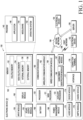
- the electronic device 101 may include a processor 120, memory 130, an input module 150, a sound output module 155, a display module 160, an audio module 170, a sensor module 176, an interface 177, a connecting terminal
- the display module 160 may include a first display module 351 corresponding to the user's left eye and/or a second display module 353 corresponding to the user's right eye., a haptic module 179, a camera module 180, a power management module 188, a battery 189, a communication module 190, a subscriber identification module (SIM) 196, or an antenna module 197.
- SIM subscriber identification module
- At least one (e.g., the connecting terminal 178) of the components may be omitted from the electronic device 101, or one or more other components may be added in the electronic device 101.
- some (e.g., the sensor module 176, the camera module 180, or the antenna module 197) of the components may be integrated into a single component (e.g., the display module 160).
- the processor 120 may execute, for example, software (e.g., a program 140) to control at least one other component (e.g., a hardware or software component) of the electronic device 101 coupled with the processor 120, and may perform various data processing or computation.
- the processor 120 may store a command or data received from another component (e.g., the sensor module 176 or the communication module 190) in volatile memory 132, process the command or the data stored in the volatile memory 132, and store resulting data in non-volatile memory 134.
- the processor 120 may include a main processor 121 (e.g., a central processing unit (CPU) or an application processor (AP)), or an auxiliary processor 123 (e.g., a graphics processing unit (GPU), a neural processing unit (NPU), an image signal processor (ISP), a sensor hub processor, or a communication processor (CP)) that is operable independently from, or in conjunction with, the main processor 121.
- a main processor 121 e.g., a central processing unit (CPU) or an application processor (AP)
- auxiliary processor 123 e.g., a graphics processing unit (GPU), a neural processing unit (NPU), an image signal processor (ISP), a sensor hub processor, or a communication processor (CP)
- the main processor 121 may be configured to use lower power than the main processor 121 or to be specified for a designated function.
- the auxiliary processor 123 may be implemented as separate from, or as part of the main processor 121.
- the auxiliary processor 123 may control at least some of functions or states related to at least one component (e.g., the display module 160, the sensor module 176, or the communication module 190) among the components of the electronic device 101, instead of the main processor 121 while the main processor 121 is in an inactive (e.g., sleep) state, or together with the main processor 121 while the main processor 121 is in an active state (e.g., executing an application).
- the auxiliary processor 123 e.g., an image signal processor or a communication processor
- the camera module 180 may capture a still image or moving images.
- the camera module 180 may include one or more lenses, image sensors, image signal processors, or flashes.
- the wireless communication module 192 may identify or authenticate the electronic device 101 in a communication network, such as the first network 198 or the second network 199, using subscriber information (e.g., international mobile subscriber identity (IMSI)) stored in the subscriber identification module 196.
- subscriber information e.g., international mobile subscriber identity (IMSI)
- the signal or the power may then be transmitted or received between the communication module 190 and the external electronic device via the selected at least one antenna.
- other parts e.g., radio frequency integrated circuit (RFIC)
- RFIC radio frequency integrated circuit
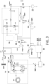
- the load switch 230 may be electrically connected to the wired power transmission/reception port 220.
- power provided from the wired power transmission/reception port 220 may be transferred to the switching charger 240 and/or the wireless power transmission/reception circuit 210.
- Power provided from the switching charger 240 may be transferred to the wired power transmission/reception port 220 through the load switch 230.
- Power provided from the wireless power transmission/reception circuit 210 may be transferred to the wired power transmission/reception port 220 through the load switch 230.
- the processor 120 may control the transfer of power between the wired power transmission/reception port 220 and the switching charger 240 by controlling the load switch 230.
- the processor 120 may control the transfer of power between the wired power transmission/reception port 220 and the wireless power transmission/reception circuit 210 by controlling the load switch 230.
- the configuration of the load switch 230 is not limited.
- the processor 120 may identify the magnitude of the current flowing from the wired power transmission/reception port 220 to the load switch 230 or the magnitude of the current flowing from the load switch 230 to the wired power transmission/reception port 220.
- the processor 120 may identify the magnitude of the current flowing through the load switch 230 by using a current mirror.
- the processor 120 may identify the voltage of the output end of the load switch 230 electrically connected to the switching charger 240. The identification of current and/or voltage is described below.
- the electronic device 101 may identify the efficiency of the switching charger 240 (for example, the efficiency may be an efficiency value or factor).
- the efficiency of the switching charger 240 may be the magnitude of the power output from the switching charger 240 relative to the magnitude of the power input to the switching charger 240 (for example, the efficiency may be a value or factor corresponding to the magnitude of the power input to the switching charger 240).
- At least some of the operations of FIG. 5 may be omitted.
- the operation order of the operations of FIG. 5 may be changed. Operations other than the operations of FIG. 5 may be performed before, during, or after the operations of FIG. 5 . At least some of the operations of FIG. 5 may correspond to at least some of the operations of FIG. 4 .
- the operations of FIG. 5 may be performed organically with the operations of FIG. 4 .
- the electronic device 101 may compare the digital information in operation 503 with the predicted (or calculated or determined or estimated) current in operation 501.
- the electronic device 101 e.g., the processor 120
- FIG. 6 is a flowchart illustrating an operation method of an electronic device according to embodiments.
- the electronic device 101 may identify (or calculate or estimate or determine) at least one error value provided by at least one error amplifier (e.g., 301, 302, 303, or 304).
- the electronic device 101 e.g., the processor 120
- a current e.g., a current between the wired power transmission/reception port 220 and the load switch 230
- a reference value e.g., a first reference value
- the electronic device 101 may identify the second error value output from the second error amplifier 302 that compares the voltage at the output end of the load switch 230 (e.g., the voltage at the end toward the switching charger 240 of the two opposite ends of the load switch 230) (e.g., the VBUS of FIG. 3 ) with a reference value (e.g., the second reference value) (e.g., the VREF2 of FIG. 3 ).
- the electronic device 101 e.g., the processor 120
- the electronic device 101 may identify a fourth error value output from the fourth error amplifier 304 that compares the current (e.g., V_I BATT of FIG. 3 ) between the switching charger 240 and the battery 250 with a reference value (e.g., a fourth reference value) (e.g., VREF4 of FIG. 3 ).
- a reference value e.g., a fourth reference value
- the electronic device 101 may select one error value from among the at least one error value (e.g., a first error value, a second error value, a third error value, and a fourth error value) provided by the at least one error amplifier (e.g., 301, 302, 303, and 304).
- the electronic device 101 e.g., the processor 120
- the electronic device 101 may control the switching charger 240 based on the error value (e.g., the minimum error value) selected in operation 603.
- the electronic device 101 e.g., the processor 120
- PWM pulse width modulation
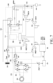
- FIG. 7 is a view illustrating operations of an electronic device according to embodiments.
- charging of the battery 250 of the electronic device 101 may be described.
- the electronic device 101 may simultaneously or separately receive the power 720 through the wired power transmission/reception port 220 and the power 710 through the wireless power transmission/reception circuit 210, and may charge the battery 250 based on the received power (e.g., 710 and/or 720).
- the electronic device 101 e.g., the processor 120
- FIG. 8 is a view illustrating operations of an electronic device according to embodiments.
- an embodiment of wirelessly transmitting power to an external device e.g., the electronic device 102 and/or the electronic device 104 of FIG. 1
- the wireless power transmission/reception circuit 210 based on power input through the wired power transmission/reception port 220 may be described.
- the electronic device 101 may provide power to the wireless power transmission/reception circuit 210, based on the power 821 input through the wired power transmission/reception port 220.
- the electronic device 101 e.g., the processor 120
- the electronic device 101 may control the switching charger 240, the load switch 230, and the wireless power transmission/reception circuit 210 to provide power to the wireless power transmission/reception circuit 210, based on the power 821 input through the wired power transmission/reception port 220.
- the electronic device 101 e.g., the processor 120
- FIG. 9 is a view illustrating operations of an electronic device according to embodiments.
- an embodiment of wiredly transmitting power to an external device e.g., the electronic device 102 of FIG. 1
- an external device e.g., the electronic device 102 of FIG. 1
- the wired power transmission/reception port 220 based on power received through the wireless power transmission/reception circuit 210 may be described.
- the electronic device 101 may provide power to the wired power transmission/reception port 220, based on the power 912 received through the wireless power transmission/reception circuit 210.
- the electronic device 101 e.g., the processor 120
- the electronic device 101 may control the switching charger 240, the load switch 230, and the wireless power transmission/reception circuit 210 to provide power to the wired power transmission/reception port 220, based on the power 912 received through the wireless power transmission/reception circuit 210.
- the electronic device 101 e.g., the processor 120
- FIG. 10 is a view illustrating operations of an electronic device according to embodiments.
- the electronic device 101 may provide power to the wired power transmission/reception port 220 and/or the wireless power transmission/reception circuit 210, based on power provided from the battery 250.
- the electronic device 101 e.g., the processor 120
- the electronic device 101 e.g., the processor 120
- the electronic device 101 may simultaneously or separately provide power to the wired power transmission/reception port 220 and the wireless power transmission/reception circuit 210, based on power provided from the battery 250.
- the electronic device 101 e.g., the processor 120
- an electronic device 101 may comprise a wireless power transmission/reception circuit 210, a wired power transmission/reception port 220, a load switch 230 electrically connected to the wired power transmission/reception port 220, a switching charger 240 electrically connected to the load switch 230 and the wireless power transmission/reception circuit 210, a battery 250 electrically connected to the switching charger 240, and a processor 120.
- the minimum selector 305 may be configured to select a smallest error value among the at least one error value.
- the processor 120 may be configured to control the switching charger 240, the load switch 230, and the wireless power transmission/reception circuit 210 to charge the battery 250 based on power input through the wired power transmission/reception port 220 and/or power received through the wireless power transmission/reception circuit 210.
- the processor 120 may be configured to control the switching charger 240, the load switch 230, and the wireless power transmission/reception circuit 210 to provide power to the wireless power transmission/reception circuit 210 based on power input through the wired power transmission/reception port 220.
- the processor 120 may be configured to control the switching charger 240, the load switch 230, and the wireless power transmission/reception circuit 210 to provide power to the wired power transmission/reception port 220 based on power received through the wireless power transmission/reception circuit 210.
- the processor 120 may be configured to control the switching charger 240, the load switch 230, and the wireless power transmission/reception circuit 210 to provide power to the wired power transmission/reception port 220 and/or the wireless power transmission/reception circuit 210 based on power provided from the battery 250.
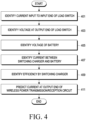
- a method for operating an electronic device 101 may comprise identifying a first current input to an input end of a load switch 230 electrically connected to a wired power transmission/reception port 220 of the electronic device 101.
- the method may comprise identifying a first voltage at an output end of the load switch 230.
- the method may comprise identifying a second voltage of a battery 250 of the electronic device 101.
- the method may comprise identifying a second current between a switching charger 240 of the electronic device 101 and the battery 250.
- the switching charger 240 may be electrically connected to a wireless power transmission/reception circuit 210 of the electronic device 101 and the load switch 230.
- the method may comprise identifying efficiency of the switching charger 240.
- the method may comprise predicting a third current at an output end 355 of the wireless power transmission/reception circuit 210 based on the first current, the first voltage, the second voltage, the second current, and the efficiency.
- the method may comprise re-predicting the third current at the output end 355 of the wireless power transmission/reception circuit 210 based on the adjusted efficiency.
- selecting the one error value may include selecting a smallest error value among the at least one error value.
- the method may comprise providing power to the wireless power transmission/reception circuit 210 based on power input through the wired power transmission/reception port 220.
- the method may comprise providing power to the wired power transmission/reception port 220 based on power received through the wireless power transmission/reception circuit 210.
- the method may comprise providing power to the wired power transmission/reception port 220 and/or the wireless power transmission/reception circuit 210 based on power provided from the battery 250.
- the at least one operation may include identifying a first current input to an input end of a load switch 230 electrically connected to a wired power transmission/reception port 220 of the electronic device 101.
- the at least one operation may include identifying a first voltage at an output end of the load switch 230.
- the at least one operation may include identifying a second voltage of a battery 250 of the electronic device 101.
- the at least one operation may include identifying a second current between a switching charger 240 of the electronic device 101 and the battery 250.
- the switching charger 240 may be electrically connected to a wireless power transmission/reception circuit 210 of the electronic device 101 and the load switch 230.
- the at least one operation may include identifying efficiency of the switching charger 240.
- the at least one operation may include predicting a third current at an output end 355 of the wireless power transmission/reception circuit 210 based on the first current, the first voltage, the second voltage, the second current, and the efficiency.
- an electronic device comprising: a wireless power transmission/reception circuit; a wired power transmission/reception port; a load switch electrically connected to the wired power transmission/reception port; a switching charger electrically connected to the load switch and the wireless power transmission/reception circuit; a battery electrically connected to the switching charger; and a processor, wherein the processor is configured to: identify a first current input to an input end of the load switch; identify a first voltage at an output end of the load switch; identify a second voltage of the battery; identify a second current between the switching charger and the battery; identify an efficiency of the switching charger, wherein the efficiency of the switching charger is the magnitude of the power output from the switching charger relative to the magnitude of the power input to the switching charger; predict a third current at an output end of the wireless power transmission/reception circuit based on the first current input, the first voltage, the second voltage, the second current, and the efficiency of the switching charger.
- the electronic device of any one of the first to the fifth example wherein the processor is configured to control the switching charger, the load switch, and the wireless power transmission/reception circuit to charge the battery based on power input through the wired power transmission/reception port and/or power received through the wireless power transmission/reception circuit.
- the electronic device of any one of the first to the sixth example is provided, wherein the processor is configured to control the switching charger, the load switch, and the wireless power transmission/reception circuit to provide power to the wireless power transmission/reception circuit based on power input through the wired power transmission/reception port.
- the electronic device of any one of the first to the seventh example wherein the processor is configured to control the switching charger, the load switch, and the wireless power transmission/reception circuit to provide power to the wired power transmission/reception port based on power received through the wireless power transmission/reception circuit.
- the electronic device of any one of the first to the eighth example is provided, wherein the processor is configured to control the switching charger, the load switch, and the wireless power transmission/reception circuit to provide power to the wired power transmission/reception port and/or the wireless power transmission/reception circuit based on power provided from the battery.
- a method for operating an electronic device comprising: identifying a first current input to an input end of a load switch electrically connected to a wired power transmission/reception port of the electronic device; identifying a first voltage at an output end of the load switch; identifying a second voltage of a battery of the electronic device; identifying a second current between a switching charger of the electronic device and the battery, the switching charger being electrically connected to a wireless power transmission/reception circuit of the electronic device and the load switch; identifying an efficiency of the switching charger; and predicting a third current at an output end of the wireless power transmission/reception circuit based on the first current, the first voltage, the second voltage, the second current, and the efficiency of the switching charger.
Landscapes
- Engineering & Computer Science (AREA)
- Power Engineering (AREA)
- Computer Networks & Wireless Communication (AREA)
- Charge And Discharge Circuits For Batteries Or The Like (AREA)
Applications Claiming Priority (3)
| Application Number | Priority Date | Filing Date | Title |
|---|---|---|---|
| KR20220155188 | 2022-11-18 | ||
| KR1020220170727A KR20240074598A (ko) | 2022-11-18 | 2022-12-08 | 스위칭 차저를 포함하는 전자 장치 및 그 동작 방법 |
| PCT/KR2023/012080 WO2024106699A1 (ko) | 2022-11-18 | 2023-08-16 | 스위칭 차저를 포함하는 전자 장치 및 그 동작 방법 |
Publications (2)
| Publication Number | Publication Date |
|---|---|
| EP4398453A1 true EP4398453A1 (de) | 2024-07-10 |
| EP4398453A4 EP4398453A4 (de) | 2025-07-16 |
Family
ID=89030032
Family Applications (1)
| Application Number | Title | Priority Date | Filing Date |
|---|---|---|---|
| EP23802137.2A Pending EP4398453A4 (de) | 2022-11-18 | 2023-08-16 | Elektronische vorrichtung mit schaltladegerät und betriebsverfahren dafür |
Country Status (3)
| Country | Link |
|---|---|
| US (1) | US20250141273A1 (de) |
| EP (1) | EP4398453A4 (de) |
| WO (1) | WO2024106699A1 (de) |
Family Cites Families (6)
| Publication number | Priority date | Publication date | Assignee | Title |
|---|---|---|---|---|
| KR101868445B1 (ko) * | 2016-02-05 | 2018-06-18 | 주식회사 알에프텍 | 유무선 충전 장치 |
| KR102269111B1 (ko) * | 2016-12-08 | 2021-06-24 | 주식회사 엘지화학 | 충전용 배터리가 구비된 무선 전자 디바이스 |
| US10523032B2 (en) * | 2017-06-22 | 2019-12-31 | Richtek Technology Corporation | Charging apparatus with multiple power paths |
| KR102584438B1 (ko) * | 2017-11-13 | 2023-10-05 | 삼성전자주식회사 | 전력의 경로를 조정하는 장치 및 그 동작 방법 |
| CN109672254B (zh) * | 2019-02-22 | 2021-01-29 | 维沃移动通信有限公司 | 一种充电控制电路、终端设备及控制方法 |
| WO2022159927A1 (en) * | 2021-01-19 | 2022-07-28 | Qualcomm Incorporated | Multi-output switched-mode power supply for multi- cell-in-series battery charging |
-
2023
- 2023-08-16 EP EP23802137.2A patent/EP4398453A4/de active Pending
- 2023-08-16 WO PCT/KR2023/012080 patent/WO2024106699A1/ko not_active Ceased
-
2025
- 2025-01-03 US US19/008,983 patent/US20250141273A1/en active Pending
Also Published As
| Publication number | Publication date |
|---|---|
| EP4398453A4 (de) | 2025-07-16 |
| WO2024106699A1 (ko) | 2024-05-23 |
| US20250141273A1 (en) | 2025-05-01 |
Similar Documents
| Publication | Publication Date | Title |
|---|---|---|
| US12113381B2 (en) | Electronic device for charging multiple batteries | |
| EP4300759B1 (de) | Elektronische vorrichtung zum laden mehrerer batterien | |
| US20240223001A1 (en) | Power transfer method and electronic apparatus for executing power transfer method | |
| US20220181889A1 (en) | Method of charging a plurality of batteries and electronic device applying the method | |
| US20230123227A1 (en) | Battery pack and method of controlling charging of the same | |
| US20250293598A1 (en) | Electronic device for controlling dc/dc converter and method for operating the electronic device | |
| US20250112503A1 (en) | Electronic device for wirelessly receiving power, and method for operating same | |
| EP4412030A1 (de) | Elektronische vorrichtung und betriebsverfahren der elektronischen vorrichtung | |
| EP4398453A1 (de) | Elektronische vorrichtung mit schaltladegerät und betriebsverfahren dafür | |
| US20230420960A1 (en) | Electronic device including battery pack, and operation method of electronic device | |
| KR20240074598A (ko) | 스위칭 차저를 포함하는 전자 장치 및 그 동작 방법 | |
| US12316154B2 (en) | Electronic device stabilizing output current of charging circuit and controlling method thereof | |
| US12132328B2 (en) | Electronic device to improve the efficiency of wireless charging | |
| EP4372959A1 (de) | Elektronische vorrichtung mit mehreren batterien und betriebsverfahren dafür | |
| US20250350140A1 (en) | Electronic device and wired/wireless charging control method in electronic device | |
| EP4593232A1 (de) | Elektronische vorrichtung und verfahren zur steuerung des ladestroms für mehrere batterien | |
| US20250192591A1 (en) | First electronic device for receiving power from second electronic device, method therefor, and second electronic device for transmitting power to first electronic device | |
| US20250149908A1 (en) | Electronic device comprising plurality of batteries and operating method therefor | |
| US20240421613A1 (en) | Electronic device and method for controlling battery charging in the electronic device | |
| US20250233441A1 (en) | Method and electronic device for charging battery | |
| EP4701043A1 (de) | Elektronische vorrichtung zur drahtlosen stromübertragung und betriebsverfahren dafür | |
| EP4325693A1 (de) | Elektronische vorrichtung und verfahren zum drahtlosen senden und empfangen von strom in einer elektronischen vorrichtung | |
| US20240022120A1 (en) | Method of providing wireless charging guide and electronic device performing same | |
| EP4708612A1 (de) | Elektronische vorrichtung zum laden einer batterie unter verwendung eines direkten ladegeräts und betriebsverfahren dafür | |
| EP4380064A1 (de) | Elektronische vorrichtung und verfahren zur verbesserung der heizleistung einer elektronischen vorrichtung |
Legal Events
| Date | Code | Title | Description |
|---|---|---|---|
| STAA | Information on the status of an ep patent application or granted ep patent |
Free format text: STATUS: UNKNOWN |
|
| STAA | Information on the status of an ep patent application or granted ep patent |
Free format text: STATUS: THE INTERNATIONAL PUBLICATION HAS BEEN MADE |
|
| PUAI | Public reference made under article 153(3) epc to a published international application that has entered the european phase |
Free format text: ORIGINAL CODE: 0009012 |
|
| STAA | Information on the status of an ep patent application or granted ep patent |
Free format text: STATUS: REQUEST FOR EXAMINATION WAS MADE |
|
| 17P | Request for examination filed |
Effective date: 20231117 |
|
| AK | Designated contracting states |
Kind code of ref document: A1 Designated state(s): AL AT BE BG CH CY CZ DE DK EE ES FI FR GB GR HR HU IE IS IT LI LT LU LV MC ME MK MT NL NO PL PT RO RS SE SI SK SM TR |
|
| A4 | Supplementary search report drawn up and despatched |
Effective date: 20250613 |
|
| RIC1 | Information provided on ipc code assigned before grant |
Ipc: H02J 50/10 20160101AFI20250606BHEP Ipc: H02J 7/00 20060101ALI20250606BHEP Ipc: H02J 7/34 20060101ALI20250606BHEP Ipc: H02M 3/155 20060101ALI20250606BHEP |
|
| DAV | Request for validation of the european patent (deleted) | ||
| DAX | Request for extension of the european patent (deleted) |