EP4398151A2 - Verfahren zur herstellung eines etiketts für ein textil - Google Patents
Verfahren zur herstellung eines etiketts für ein textil Download PDFInfo
- Publication number
- EP4398151A2 EP4398151A2 EP24177742.4A EP24177742A EP4398151A2 EP 4398151 A2 EP4398151 A2 EP 4398151A2 EP 24177742 A EP24177742 A EP 24177742A EP 4398151 A2 EP4398151 A2 EP 4398151A2
- Authority
- EP
- European Patent Office
- Prior art keywords
- radio module
- integrated circuit
- substrate
- antenna
- uhf
- Prior art date
- Legal status (The legal status is an assumption and is not a legal conclusion. Google has not performed a legal analysis and makes no representation as to the accuracy of the status listed.)
- Pending
Links
Images
Classifications
-
- G—PHYSICS
- G06—COMPUTING OR CALCULATING; COUNTING
- G06K—GRAPHICAL DATA READING; PRESENTATION OF DATA; RECORD CARRIERS; HANDLING RECORD CARRIERS
- G06K19/00—Record carriers for use with machines and with at least a part designed to carry digital markings
- G06K19/02—Record carriers for use with machines and with at least a part designed to carry digital markings characterised by the selection of materials, e.g. to avoid wear during transport through the machine
- G06K19/027—Record carriers for use with machines and with at least a part designed to carry digital markings characterised by the selection of materials, e.g. to avoid wear during transport through the machine the material being suitable for use as a textile, e.g. woven-based RFID-like labels designed for attachment to laundry items
-
- G—PHYSICS
- G06—COMPUTING OR CALCULATING; COUNTING
- G06K—GRAPHICAL DATA READING; PRESENTATION OF DATA; RECORD CARRIERS; HANDLING RECORD CARRIERS
- G06K19/00—Record carriers for use with machines and with at least a part designed to carry digital markings
- G06K19/06—Record carriers for use with machines and with at least a part designed to carry digital markings characterised by the kind of the digital marking, e.g. shape, nature, code
- G06K19/067—Record carriers with conductive marks, printed circuits or semiconductor circuit elements, e.g. credit or identity cards also with resonating or responding marks without active components
- G06K19/07—Record carriers with conductive marks, printed circuits or semiconductor circuit elements, e.g. credit or identity cards also with resonating or responding marks without active components with integrated circuit chips
- G06K19/077—Constructional details, e.g. mounting of circuits in the carrier
- G06K19/07749—Constructional details, e.g. mounting of circuits in the carrier the record carrier being capable of non-contact communication, e.g. constructional details of the antenna of a non-contact smart card
- G06K19/07773—Antenna details
-
- G—PHYSICS
- G06—COMPUTING OR CALCULATING; COUNTING
- G06K—GRAPHICAL DATA READING; PRESENTATION OF DATA; RECORD CARRIERS; HANDLING RECORD CARRIERS
- G06K19/00—Record carriers for use with machines and with at least a part designed to carry digital markings
- G06K19/06—Record carriers for use with machines and with at least a part designed to carry digital markings characterised by the kind of the digital marking, e.g. shape, nature, code
- G06K19/067—Record carriers with conductive marks, printed circuits or semiconductor circuit elements, e.g. credit or identity cards also with resonating or responding marks without active components
- G06K19/07—Record carriers with conductive marks, printed circuits or semiconductor circuit elements, e.g. credit or identity cards also with resonating or responding marks without active components with integrated circuit chips
- G06K19/077—Constructional details, e.g. mounting of circuits in the carrier
- G06K19/0772—Physical layout of the record carrier
- G06K19/07722—Physical layout of the record carrier the record carrier being multilayered, e.g. laminated sheets
-
- G—PHYSICS
- G06—COMPUTING OR CALCULATING; COUNTING
- G06K—GRAPHICAL DATA READING; PRESENTATION OF DATA; RECORD CARRIERS; HANDLING RECORD CARRIERS
- G06K19/00—Record carriers for use with machines and with at least a part designed to carry digital markings
- G06K19/06—Record carriers for use with machines and with at least a part designed to carry digital markings characterised by the kind of the digital marking, e.g. shape, nature, code
- G06K19/067—Record carriers with conductive marks, printed circuits or semiconductor circuit elements, e.g. credit or identity cards also with resonating or responding marks without active components
- G06K19/07—Record carriers with conductive marks, printed circuits or semiconductor circuit elements, e.g. credit or identity cards also with resonating or responding marks without active components with integrated circuit chips
- G06K19/077—Constructional details, e.g. mounting of circuits in the carrier
- G06K19/0772—Physical layout of the record carrier
- G06K19/07728—Physical layout of the record carrier the record carrier comprising means for protection against impact or bending, e.g. protective shells or stress-absorbing layers around the integrated circuit
-
- G—PHYSICS
- G06—COMPUTING OR CALCULATING; COUNTING
- G06K—GRAPHICAL DATA READING; PRESENTATION OF DATA; RECORD CARRIERS; HANDLING RECORD CARRIERS
- G06K19/00—Record carriers for use with machines and with at least a part designed to carry digital markings
- G06K19/06—Record carriers for use with machines and with at least a part designed to carry digital markings characterised by the kind of the digital marking, e.g. shape, nature, code
- G06K19/067—Record carriers with conductive marks, printed circuits or semiconductor circuit elements, e.g. credit or identity cards also with resonating or responding marks without active components
- G06K19/07—Record carriers with conductive marks, printed circuits or semiconductor circuit elements, e.g. credit or identity cards also with resonating or responding marks without active components with integrated circuit chips
- G06K19/077—Constructional details, e.g. mounting of circuits in the carrier
- G06K19/07749—Constructional details, e.g. mounting of circuits in the carrier the record carrier being capable of non-contact communication, e.g. constructional details of the antenna of a non-contact smart card
- G06K19/0775—Constructional details, e.g. mounting of circuits in the carrier the record carrier being capable of non-contact communication, e.g. constructional details of the antenna of a non-contact smart card arrangements for connecting the integrated circuit to the antenna
Definitions
- the present invention relates to a method for manufacturing a tag for a fabric, in particular, but not exclusively a tag for identification of a garment associated with it, for example for identification of the garment in a laundry.
- the garment must be able to be identified, for example within a laundry, during a washing or treatment process where it is required to be able to identify the owner of the garment, among other things in order to be able to return the garment to the owner, following treatment.
- the package is then integrated with the other components of the tag, by the tag manufacturer, and therefore by a company different from the microcircuit manufacturer.
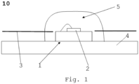
- Figure 1 shows in schematic form a tag for a fabric according to the present invention.
- this procedural step also comprises the partial coating of the tag antenna, in the area of the substrate immediately surrounding the module and the circuit, thus ensuring also the positioning of the antenna relative to the module and the circuit.
- the manufacturing method according to the prior art instead, involves incorporating all the electronic components necessary for tracking, including the long-range antenna and the microchip, in a so-called "inlay” and associating the inlay with multiple layers, such as an adhesive layer situated underneath the inlay, a silicone layer situated underneath the adhesive layer and a PET layer situated above the inlay, and finally fixing the multilayer structure thus formed to the fabric to be tracked, for example by means of heat welding.
- the inlay according to the prior art incorporates the chip and the antenna, made of aluminium, copper or silver, and these components may not be applied separately to a textile support (or support made of other material) as is instead envisaged by the present invention.
- the support substrate according to the present invention is preferably a textile substrate.
- the aforementioned material is not limiting.
- the fabric to be tracked may be fixed to the tag by means of stitching of the fabrics (i.e. fabric of the textile substrate of the tag and fabric of the garment to be tracked). Such a fixing method is not limiting.
- the tag 10 comprises:
- the method comprises the steps of:
- the step of applying the protective coating 5 further comprises:
- the step of applying the protective coating 5 comprises, for example:
- the protective coating 5 becomes rigid at the end of the solidification step.
- the antenna portion intended to be coated by the protective coating 5 forms a shoulder for containing the coating 5, for example the glue or the resin, therefore preventing dispersion thereof in areas of the substrate relatively far from the UHF radio module 1 and from the RFID integrated circuit 2, thus allowing the entire predefined amount of protective coating 5 to be used in the areas to be protected.
- the antenna portion intended for the coating increases the adhesion of the protective coating material.
- the term "protective coating 5" used in the present invention does not indicate necessarily a coating which adheres perfectly to the UHF radio module 1 and the RFID integrated circuit 2, as in the case of a glue or resin, but may also indicate a covering of said UHF radio module 1 and RFID integrated circuit 2 which is, at least partly, not in contact with the UHF radio module 1 and the RFID integrated circuit 2, and also not in direct with the metal tracks for electrical connection thereof, or at least not in contact along the entire length of the metal tracks, but which is nevertheless designed to protect the electrical connection thereof with the UHF radio module 1 and the RFID integrated circuit 2 and to cover at least a surface portion of the substrate 4 situated around the UHF radio module 1 and the RFID integrated circuit 2, so as to protect also the structural interconnection between the UHF radio module 1 and the substrate 4 and keep the UHF radio module 1 and the RFID integrated circuit 2 in a fixed position on the substrate 4.
- the UHF radio module 1 comprises a PCB (printed circuit board) which incorporates metal tracks intended to act as a short-range inductor.
- the RFID integrated circuit 2 is already electrically connected to the metal tracks of the UHF radio module 1 before the step of mounting the UHF radio module 1 and the RFID integrated circuit 2 on the substrate 4, said metal tracks however being exposed or not coated with any resin before the step of mounting the UHF radio module 1 and the RFID integrated circuit 2.
Landscapes
- Engineering & Computer Science (AREA)
- Microelectronics & Electronic Packaging (AREA)
- Computer Hardware Design (AREA)
- Physics & Mathematics (AREA)
- General Physics & Mathematics (AREA)
- Theoretical Computer Science (AREA)
- Computer Networks & Wireless Communication (AREA)
- Textile Engineering (AREA)
- Details Of Aerials (AREA)
- Near-Field Transmission Systems (AREA)
- Credit Cards Or The Like (AREA)
- Treatment Of Fiber Materials (AREA)
- Fishing Rods (AREA)
Applications Claiming Priority (3)
| Application Number | Priority Date | Filing Date | Title |
|---|---|---|---|
| IT102020000013294A IT202000013294A1 (it) | 2020-06-04 | 2020-06-04 | Metodo di produzione di un marcatore per un tessuto |
| PCT/IB2021/054829 WO2021245567A1 (en) | 2020-06-04 | 2021-06-02 | Method for manufacturing a tag for a textile |
| EP21732983.8A EP4162398B1 (de) | 2020-06-04 | 2021-06-02 | Verfahren zur herstellung eines etiketts für ein textil |
Related Parent Applications (2)
| Application Number | Title | Priority Date | Filing Date |
|---|---|---|---|
| EP21732983.8A Division-Into EP4162398B1 (de) | 2020-06-04 | 2021-06-02 | Verfahren zur herstellung eines etiketts für ein textil |
| EP21732983.8A Division EP4162398B1 (de) | 2020-06-04 | 2021-06-02 | Verfahren zur herstellung eines etiketts für ein textil |
Publications (2)
| Publication Number | Publication Date |
|---|---|
| EP4398151A2 true EP4398151A2 (de) | 2024-07-10 |
| EP4398151A3 EP4398151A3 (de) | 2024-09-11 |
Family
ID=72179062
Family Applications (2)
| Application Number | Title | Priority Date | Filing Date |
|---|---|---|---|
| EP21732983.8A Active EP4162398B1 (de) | 2020-06-04 | 2021-06-02 | Verfahren zur herstellung eines etiketts für ein textil |
| EP24177742.4A Pending EP4398151A3 (de) | 2020-06-04 | 2021-06-02 | Verfahren zur herstellung eines etiketts für ein textil |
Family Applications Before (1)
| Application Number | Title | Priority Date | Filing Date |
|---|---|---|---|
| EP21732983.8A Active EP4162398B1 (de) | 2020-06-04 | 2021-06-02 | Verfahren zur herstellung eines etiketts für ein textil |
Country Status (6)
| Country | Link |
|---|---|
| US (1) | US11861443B2 (de) |
| EP (2) | EP4162398B1 (de) |
| JP (1) | JP7657813B2 (de) |
| BR (1) | BR112022009446A2 (de) |
| IT (1) | IT202000013294A1 (de) |
| WO (1) | WO2021245567A1 (de) |
Families Citing this family (1)
| Publication number | Priority date | Publication date | Assignee | Title |
|---|---|---|---|---|
| EP4479883B1 (de) * | 2022-06-01 | 2025-11-12 | Datamars SA | Rfid (funkfrequenzidentifikation)-etikett, insbesondere für waschbare gegenstände |
Family Cites Families (17)
| Publication number | Priority date | Publication date | Assignee | Title |
|---|---|---|---|---|
| US20050183990A1 (en) * | 2004-01-12 | 2005-08-25 | Corbett Bradford G.Jr. | Textile identification system with RFID tracking |
| JP2009289003A (ja) | 2008-05-29 | 2009-12-10 | Panasonic Corp | Rfidタグ |
| US8162213B2 (en) * | 2008-07-25 | 2012-04-24 | G&K Services, Inc. | Article identification system with faraday screens |
| US8593256B2 (en) * | 2009-06-23 | 2013-11-26 | Avery Dennison Corporation | Washable RFID device for apparel tracking |
| CN201654823U (zh) * | 2009-12-01 | 2010-11-24 | 中山达华智能科技股份有限公司 | 一种rfid柔性洗衣标识用电子标签 |
| JP5850704B2 (ja) | 2011-10-27 | 2016-02-03 | サトーホールディングス株式会社 | 柔軟素材製品用rfidタグのrfidアンテナ |
| US9064199B2 (en) | 2011-10-27 | 2015-06-23 | Sato Holdings Kabushiki Kaisha | RFID tag for flexible material product, RFID antenna of RFID tag for flexible material product, and RFID antenna continuum of same |
| US10163054B2 (en) * | 2011-11-10 | 2018-12-25 | Amb I.T. Holding B.V. | Tag assembly |
| JP5924011B2 (ja) | 2012-02-09 | 2016-05-25 | Nok株式会社 | Icタグ |
| JP5952609B2 (ja) * | 2012-03-28 | 2016-07-13 | トッパン・フォームズ株式会社 | 非接触型データ受送信体 |
| WO2017110570A1 (ja) * | 2015-12-21 | 2017-06-29 | 株式会社村田製作所 | 部品内蔵デバイス、rfidタグ、および部品内蔵デバイスの製造方法 |
| IT201600072003A1 (it) * | 2016-07-12 | 2018-01-12 | Exteryo Srl | Dispositivo elettronico a radiofrequenza termosaldabile su supporti tessili o polimerici e sue varianti. |
| RO133013B1 (ro) * | 2017-06-16 | 2020-09-30 | Promar Textil Industries S.R.L. | Etichetă rfid pentru medii agresive cu cuplaj inductiv în buclă dublă |
| JP6440333B1 (ja) | 2017-06-28 | 2018-12-19 | 一般社団法人白亜会 | Rfidタグ及びrfidタグの製造方法 |
| US10130524B1 (en) * | 2017-06-30 | 2018-11-20 | Chung-Ping Lai | Wireless detectable diaper and monitoring equipment thereof |
| CN207249709U (zh) * | 2017-07-14 | 2018-04-17 | 杭州思创汇联科技有限公司 | 一种用于洗衣管理的uhf rfid标签 |
| DE212019000392U1 (de) | 2018-10-15 | 2021-05-20 | Murata Manufacturing Co., Ltd. | Herstellungsapparat für eine drahtlose Kommunikationsvorrichtung |
-
2020
- 2020-06-04 IT IT102020000013294A patent/IT202000013294A1/it unknown
-
2021
- 2021-06-02 EP EP21732983.8A patent/EP4162398B1/de active Active
- 2021-06-02 BR BR112022009446A patent/BR112022009446A2/pt unknown
- 2021-06-02 WO PCT/IB2021/054829 patent/WO2021245567A1/en not_active Ceased
- 2021-06-02 JP JP2022551312A patent/JP7657813B2/ja active Active
- 2021-06-02 US US17/801,596 patent/US11861443B2/en active Active
- 2021-06-02 EP EP24177742.4A patent/EP4398151A3/de active Pending
Also Published As
| Publication number | Publication date |
|---|---|
| EP4162398B1 (de) | 2024-11-13 |
| WO2021245567A1 (en) | 2021-12-09 |
| IT202000013294A1 (it) | 2021-12-04 |
| EP4162398A1 (de) | 2023-04-12 |
| US20230351141A1 (en) | 2023-11-02 |
| BR112022009446A2 (pt) | 2022-12-13 |
| US11861443B2 (en) | 2024-01-02 |
| JP7657813B2 (ja) | 2025-04-07 |
| EP4162398C0 (de) | 2024-11-13 |
| JP2023533630A (ja) | 2023-08-04 |
| EP4398151A3 (de) | 2024-09-11 |
Similar Documents
| Publication | Publication Date | Title |
|---|---|---|
| US7205899B2 (en) | Flexible transponder label which is readable on conductive surfaces | |
| KR100686573B1 (ko) | Rfid 태그 | |
| US8672230B2 (en) | RFID tag | |
| CN101689253B (zh) | 具有用于天线的连接部件的射频识别收发器芯片模块、具有射频识别收发器芯片模块的纺织标签和射频识别收发器芯片模块的使用 | |
| US20110011939A1 (en) | Contact-less and dual interface inlays and methods for producing the same | |
| EP3719707B1 (de) | Drahtlose kommunikationsvorrichtung, verfahren zu ihrer herstellung | |
| US10467516B2 (en) | Component built-in device | |
| US20070164867A1 (en) | Thin ic tag and method for manufacturing same | |
| CN113728330B (zh) | 用于芯片卡的生物识别传感器模块及所述模块的制造方法 | |
| KR102914017B1 (ko) | 스마트 ic 기판, 스마트 ic 모듈 및 이를 포함하는 ic 카드 | |
| US20150154488A1 (en) | Radio frequency identification tag and method of manufacturing the same | |
| KR20140068209A (ko) | Rfid 태그 | |
| US20150339565A1 (en) | Smart card module, smart card, and method for producing a smart card module | |
| US12361256B2 (en) | RFID assembly and tag and method of manufacturing a product using the same | |
| CA2350705C (en) | Non-contact data carrier and ic chip | |
| CN113348469A (zh) | 无线通信器件及其制造方法 | |
| EP4162398B1 (de) | Verfahren zur herstellung eines etiketts für ein textil | |
| PL203214B1 (pl) | Elektroniczna etykieta | |
| CN103380432B (zh) | 无线ic器件及其制造方法 | |
| US20090079068A1 (en) | Methods for attaching a flip chip integrated circuit assembly to a substrate | |
| US12468916B2 (en) | RFID (radio frequency identification) tag, in particular for washable items | |
| KR102896213B1 (ko) | 스마트카드에 통합하기 위한 표면 실장 커패시터를 갖는 인쇄 회로 | |
| KR101098289B1 (ko) | Rfid 태그, 이의 제작방법, 이를 이용한 패키징 구조체 및 제작방법 | |
| KR20260021660A (ko) | 스마트 ic 기판, 스마트 ic 모듈 및 이를 포함하는 ic 카드 | |
| EP3079105B1 (de) | Chipkarte mit doppelschnittstellenkomponenten und verfahren zur herstellung der chipkarte mit doppelschnittstellenkomponenten |
Legal Events
| Date | Code | Title | Description |
|---|---|---|---|
| PUAI | Public reference made under article 153(3) epc to a published international application that has entered the european phase |
Free format text: ORIGINAL CODE: 0009012 |
|
| STAA | Information on the status of an ep patent application or granted ep patent |
Free format text: STATUS: THE APPLICATION HAS BEEN PUBLISHED |
|
| AC | Divisional application: reference to earlier application |
Ref document number: 4162398 Country of ref document: EP Kind code of ref document: P |
|
| AK | Designated contracting states |
Kind code of ref document: A2 Designated state(s): AL AT BE BG CH CY CZ DE DK EE ES FI FR GB GR HR HU IE IS IT LI LT LU LV MC MK MT NL NO PL PT RO RS SE SI SK SM TR |
|
| REG | Reference to a national code |
Ref country code: DE Ref legal event code: R079 Free format text: PREVIOUS MAIN CLASS: G06K0019077000 Ipc: G06K0019020000 |
|
| PUAL | Search report despatched |
Free format text: ORIGINAL CODE: 0009013 |
|
| AK | Designated contracting states |
Kind code of ref document: A3 Designated state(s): AL AT BE BG CH CY CZ DE DK EE ES FI FR GB GR HR HU IE IS IT LI LT LU LV MC MK MT NL NO PL PT RO RS SE SI SK SM TR |
|
| RIC1 | Information provided on ipc code assigned before grant |
Ipc: G06K 19/077 20060101ALI20240805BHEP Ipc: G06K 19/02 20060101AFI20240805BHEP |
|
| STAA | Information on the status of an ep patent application or granted ep patent |
Free format text: STATUS: REQUEST FOR EXAMINATION WAS MADE |
|
| 17P | Request for examination filed |
Effective date: 20250310 |
|
| STAA | Information on the status of an ep patent application or granted ep patent |
Free format text: STATUS: EXAMINATION IS IN PROGRESS |
|
| 17Q | First examination report despatched |
Effective date: 20251030 |