EP4397992A1 - Optischer festkörpersensor und vorrichtung zur messung eines abstands mit diesem sensor - Google Patents
Optischer festkörpersensor und vorrichtung zur messung eines abstands mit diesem sensor Download PDFInfo
- Publication number
- EP4397992A1 EP4397992A1 EP23150189.1A EP23150189A EP4397992A1 EP 4397992 A1 EP4397992 A1 EP 4397992A1 EP 23150189 A EP23150189 A EP 23150189A EP 4397992 A1 EP4397992 A1 EP 4397992A1
- Authority
- EP
- European Patent Office
- Prior art keywords
- optical sensor
- photosensitive
- microcell
- microcells
- electrical
- Prior art date
- Legal status (The legal status is an assumption and is not a legal conclusion. Google has not performed a legal analysis and makes no representation as to the accuracy of the status listed.)
- Withdrawn
Links
Images


Classifications
-
- G—PHYSICS
- G01—MEASURING; TESTING
- G01S—RADIO DIRECTION-FINDING; RADIO NAVIGATION; DETERMINING DISTANCE OR VELOCITY BY USE OF RADIO WAVES; LOCATING OR PRESENCE-DETECTING BY USE OF THE REFLECTION OR RERADIATION OF RADIO WAVES; ANALOGOUS ARRANGEMENTS USING OTHER WAVES
- G01S7/00—Details of systems according to groups G01S13/00, G01S15/00, G01S17/00
- G01S7/48—Details of systems according to groups G01S13/00, G01S15/00, G01S17/00 of systems according to group G01S17/00
- G01S7/483—Details of pulse systems
- G01S7/486—Receivers
- G01S7/4861—Circuits for detection, sampling, integration or read-out
- G01S7/4863—Detector arrays, e.g. charge-transfer gates
-
- G—PHYSICS
- G01—MEASURING; TESTING
- G01S—RADIO DIRECTION-FINDING; RADIO NAVIGATION; DETERMINING DISTANCE OR VELOCITY BY USE OF RADIO WAVES; LOCATING OR PRESENCE-DETECTING BY USE OF THE REFLECTION OR RERADIATION OF RADIO WAVES; ANALOGOUS ARRANGEMENTS USING OTHER WAVES
- G01S17/00—Systems using the reflection or reradiation of electromagnetic waves other than radio waves, e.g. lidar systems
- G01S17/02—Systems using the reflection of electromagnetic waves other than radio waves
- G01S17/06—Systems determining position data of a target
- G01S17/08—Systems determining position data of a target for measuring distance only
- G01S17/10—Systems determining position data of a target for measuring distance only using transmission of interrupted, pulse-modulated waves
- G01S17/18—Systems determining position data of a target for measuring distance only using transmission of interrupted, pulse-modulated waves wherein range gates are used
-
- G—PHYSICS
- G01—MEASURING; TESTING
- G01S—RADIO DIRECTION-FINDING; RADIO NAVIGATION; DETERMINING DISTANCE OR VELOCITY BY USE OF RADIO WAVES; LOCATING OR PRESENCE-DETECTING BY USE OF THE REFLECTION OR RERADIATION OF RADIO WAVES; ANALOGOUS ARRANGEMENTS USING OTHER WAVES
- G01S7/00—Details of systems according to groups G01S13/00, G01S15/00, G01S17/00
- G01S7/48—Details of systems according to groups G01S13/00, G01S15/00, G01S17/00 of systems according to group G01S17/00
- G01S7/51—Display arrangements
-
- H—ELECTRICITY
- H10—SEMICONDUCTOR DEVICES; ELECTRIC SOLID-STATE DEVICES NOT OTHERWISE PROVIDED FOR
- H10F—INORGANIC SEMICONDUCTOR DEVICES SENSITIVE TO INFRARED RADIATION, LIGHT, ELECTROMAGNETIC RADIATION OF SHORTER WAVELENGTH OR CORPUSCULAR RADIATION
- H10F39/00—Integrated devices, or assemblies of multiple devices, comprising at least one element covered by group H10F30/00, e.g. radiation detectors comprising photodiode arrays
- H10F39/10—Integrated devices
- H10F39/107—Integrated devices having multiple elements covered by H10F30/00 in a repetitive configuration, e.g. radiation detectors comprising photodiode arrays
-
- H—ELECTRICITY
- H10—SEMICONDUCTOR DEVICES; ELECTRIC SOLID-STATE DEVICES NOT OTHERWISE PROVIDED FOR
- H10F—INORGANIC SEMICONDUCTOR DEVICES SENSITIVE TO INFRARED RADIATION, LIGHT, ELECTROMAGNETIC RADIATION OF SHORTER WAVELENGTH OR CORPUSCULAR RADIATION
- H10F39/00—Integrated devices, or assemblies of multiple devices, comprising at least one element covered by group H10F30/00, e.g. radiation detectors comprising photodiode arrays
- H10F39/80—Constructional details of image sensors
- H10F39/803—Pixels having integrated switching, control, storage or amplification elements
Definitions
- such a photosensitive microcell detects a photon and generates an electrical detection signal
- a microcell is no longer able to detect other photons until its polarization voltage is restored, either actively or passively. Since it takes some time for the polarization of a photosensitive microcell to be restored, when it detects a photon, the sensitivity of this sensor to the incidence of further photons is temporarily reduced until this microcell is restored. Furthermore, when a light radiation strikes the sensitive surface of such a sensor, the first photons of the radiation striking this surface are detected by almost all of the microcells of the sensor.
- Such a device comprises emission means of a light radiation configured to emit such light radiation in the direction of a reference object.
- Said device also comprises at least one solid-state optical sensor configured to detect the incidence of one or more photons of said light radiation that are reflected from said reference object.
- said device also comprises an electronic board configured to control the emission of said light radiation by the emission means, acquire in input the electrical signals generated by said at least one optical sensor and determine the distance between a first point of said device and a second point of said reference object based on the acquired electrical signals. For this distance to be determined, the device measures the time interval, also known as Time of Flight (ToF), that elapses between the start of the emission of such radiation by the emission means and the detection of the same radiation by the optical sensors.
- TOF Time of Flight
- an optical solid-state sensor according to the invention is indicated as a whole with the number 10 .
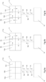
- This optical sensor 10 clearly visible in figures 1 and 2 , is configured to detect the incidence of one or more photons of a light radiation R during an acquisition window Ta .
- Said optical sensor 10 comprises a silicon plate 11 , also represented in figures 1 and 2 .
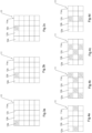
- the photosensitive microcells 12a, 12b, 12c are distributed on said sensitive surface 11a with a matrix structure of five rows and five columns.
- Each microcell of such a plurality of photosensitive microcells 12a, 12b, 12c is adapted to respectively generate an electrical detection signal Ua , Ub , Uc when a photon is detected.
- Said optical sensor 10 also comprises a control unit 14 , clearly visible in figures 1 and 2 , configured to acquire such electrical detection signals Ua , Ub, Uc in input.
- a control unit 14 is capable of processing such electrical detection signals Ua , Ub , Uc and is configured to generate at least one output electrical signal V obtained from a processing of such electrical detection signals Ua, Ub, Uc .
- the optical sensor 10 is configured to perform the following operating steps:
- This first embodiment example shows how an optical sensor 10 according to the invention solves the problem related to the "pile-up distortion" phenomenon, since only a part of the plurality of photosensitive microcells 12a, 12b, 12c of said optical sensor 10 is active at each instant of the acquisition window Ta.
- the enablement of the microcells is carried out by the control unit 14 which is capable of controlling the instant of activation of each of said plurality of photosensitive microcells 12a, 12b, 12c by means of the electrical enable signal Ea, Eb, Ec.
- the control unit 14 will activate a different inactive microcell by means of an electrical enable signal Ea, Eb, Ec.
- the control unit 14 is capable of controlling the instant of activation of at least one of such plurality of photosensitive microcells 12a, 12b, 12c by means of the electrical enable signal Ea, Eb, Ec.
- at least one first photosensitive microcell of such a plurality of photosensitive microcells 12a, 12b, 12c is connected in series to at least one second photosensitive microcell. This allows to obtain a "decentralized" enablement of the microcells, allowing the control of the instant of activation of said at least one second photosensitive microcell by said first photosensitive microcell by generating one of the aforesaid electrical detection signals Ua, Ub, Uc. Therefore, these electrical detection Ua, Ub, Uc, as can be clearly seen from Figure 5b , also act as electrical enable signals Ea, Eb, Ec, being directly responsible for the activation of inactive microcells.
- a variant of the latter embodiment of the invention still provides that each of said photosensitive microcells is connected in series to at least one different photosensitive microcell, as represented in Figure 5c .
- This allows to obtain a "cyclic" enablement of the photosensitive microcells that does not limit the acquisition window Ta to a single activation of each microcell, allowing the last microcell of the series to control the instant of activation of the first microcell in the series.
- the last microcell of the series in conjunction with the generation of the corresponding electrical detection signal, will generate an electrical enable signal Ea' enabling the microcell 12a again.
- Each microcell of such a plurality of photosensitive microcells 12a, 12b, 12c comprises a Single-Photon Avalanche Diode (SPAD), respectively 13a, 13b and 13c, as represented in Figures 1 and 2 .
- Each microcell of such a plurality of photosensitive microcells 12a, 12b, 12c is thus adapted to generate an electrical detection signal Ua, Ub, Uc when a photon is detected by the respective Single-Photon Avalanche Diode 13a, 13b and 13c.
- a device for measuring 100 a distance d, clearly visible in Figure 2 comprising at least one optical sensor 10 as described above, is also an object of the invention.
- said measuring device 100 comprises emission means 110, visible in figure 2 , of a light radiation R configured to emit said light radiation R with a duration equal to an emission window Te in the direction of a reference object O.
- emission means 110 comprise a laser emitter.
- said measuring device 100 also comprises at least one solid-state optical sensor 10, also visible in Figure 2 , configured to detect the incidence of one or more photons of said light radiation R that are reflected by said reference object O in the direction of said at least one optical sensor 10 during an acquisition window Ta.
- a measuring device 100 comprises a single optical sensor 10.
- the use of a plurality of optical sensors 10 cannot be excluded in other embodiments of the invention.
Landscapes
- Engineering & Computer Science (AREA)
- Physics & Mathematics (AREA)
- Computer Networks & Wireless Communication (AREA)
- General Physics & Mathematics (AREA)
- Radar, Positioning & Navigation (AREA)
- Remote Sensing (AREA)
- Electromagnetism (AREA)
- Optical Radar Systems And Details Thereof (AREA)
Priority Applications (1)
| Application Number | Priority Date | Filing Date | Title |
|---|---|---|---|
| EP23150189.1A EP4397992A1 (de) | 2023-01-03 | 2023-01-03 | Optischer festkörpersensor und vorrichtung zur messung eines abstands mit diesem sensor |
Applications Claiming Priority (1)
| Application Number | Priority Date | Filing Date | Title |
|---|---|---|---|
| EP23150189.1A EP4397992A1 (de) | 2023-01-03 | 2023-01-03 | Optischer festkörpersensor und vorrichtung zur messung eines abstands mit diesem sensor |
Publications (1)
| Publication Number | Publication Date |
|---|---|
| EP4397992A1 true EP4397992A1 (de) | 2024-07-10 |
Family
ID=84829613
Family Applications (1)
| Application Number | Title | Priority Date | Filing Date |
|---|---|---|---|
| EP23150189.1A Withdrawn EP4397992A1 (de) | 2023-01-03 | 2023-01-03 | Optischer festkörpersensor und vorrichtung zur messung eines abstands mit diesem sensor |
Country Status (1)
| Country | Link |
|---|---|
| EP (1) | EP4397992A1 (de) |
Citations (2)
| Publication number | Priority date | Publication date | Assignee | Title |
|---|---|---|---|---|
| CN105606232A (zh) * | 2016-01-28 | 2016-05-25 | 中国人民解放军信息工程大学 | 一种探测光信号的实现方法及系统 |
| WO2021258106A1 (en) * | 2020-06-15 | 2021-12-23 | Continental Automotive Systems, Inc. | Lidar system |
-
2023
- 2023-01-03 EP EP23150189.1A patent/EP4397992A1/de not_active Withdrawn
Patent Citations (2)
| Publication number | Priority date | Publication date | Assignee | Title |
|---|---|---|---|---|
| CN105606232A (zh) * | 2016-01-28 | 2016-05-25 | 中国人民解放军信息工程大学 | 一种探测光信号的实现方法及系统 |
| WO2021258106A1 (en) * | 2020-06-15 | 2021-12-23 | Continental Automotive Systems, Inc. | Lidar system |
Similar Documents
| Publication | Publication Date | Title |
|---|---|---|
| CN110888117B (zh) | 使用多个雪崩光电二极管元件检测光 | |
| US20210302553A1 (en) | Lidar systems with improved time-to-digital conversion circuitry | |
| US20060192086A1 (en) | Integrated imager circuit comprising a monolithic array of single photon avalanche diodes | |
| JP2019032305A (ja) | 距離を計測するための光電センサ及び方法 | |
| JP2019049531A (ja) | 距離を計測するための装置及び前記距離を計測するための方法 | |
| TW201600875A (zh) | 具有可重新組態的光二極體陣列的光學近接感測器 | |
| TWI748460B (zh) | 飛時測距裝置及飛時測距方法 | |
| EP4018218B1 (de) | Infrarotbildgebungsanordnung | |
| JP2018173379A (ja) | 光検出器及び測距装置 | |
| KR20160092137A (ko) | 티오에프 방식의 거리 측정 장치에서 제어 방법 | |
| CA3085648C (en) | Arrangement and method for determining a distance of at least one object using light signals | |
| WO2019176752A1 (ja) | 光検出装置、光検出方法および光学式測距センサ | |
| CN111624615B (zh) | 光传感器 | |
| US12196860B2 (en) | Depth sensor calibration using internal reflections | |
| CN112346076A (zh) | 电子装置的控制方法、电子装置及计算机可读存储介质 | |
| EP3948344B1 (de) | Ereignisgesteuertes gemeinsam genutztes speicherpixel | |
| Jahromi et al. | A single chip laser radar receiver with a 9× 9 SPAD detector array and a 10-channel TDC | |
| EP4397992A1 (de) | Optischer festkörpersensor und vorrichtung zur messung eines abstands mit diesem sensor | |
| CN115201781A (zh) | 激光雷达传感器和从其中去除噪声的方法 | |
| CN114089355A (zh) | 探测装置及方法 | |
| JP7101529B2 (ja) | 光センサおよび電子機器 | |
| US12529772B2 (en) | Time-of-flight imaging system and method and computer program for operating a time-of-flight imaging system | |
| CN113759344B (zh) | 直接飞行时间dtof传感器的感测控制装置和方法 | |
| EP3977157B1 (de) | Festkörper-bildsensor mit hoher räumlicher auflösung mit verteiltem fotovervielfacher | |
| EP4511676B1 (de) | Verbesserte vorrichtung zur messung des abstandes zwischen derselben vorrichtung und einem referenzobjekt mittels lichtstrahlung |
Legal Events
| Date | Code | Title | Description |
|---|---|---|---|
| PUAI | Public reference made under article 153(3) epc to a published international application that has entered the european phase |
Free format text: ORIGINAL CODE: 0009012 |
|
| STAA | Information on the status of an ep patent application or granted ep patent |
Free format text: STATUS: THE APPLICATION HAS BEEN PUBLISHED |
|
| AK | Designated contracting states |
Kind code of ref document: A1 Designated state(s): AL AT BE BG CH CY CZ DE DK EE ES FI FR GB GR HR HU IE IS IT LI LT LU LV MC ME MK MT NL NO PL PT RO RS SE SI SK SM TR |
|
| STAA | Information on the status of an ep patent application or granted ep patent |
Free format text: STATUS: THE APPLICATION IS DEEMED TO BE WITHDRAWN |
|
| 18D | Application deemed to be withdrawn |
Effective date: 20250111 |