EP4397618A1 - Microchannel chip - Google Patents
Microchannel chip Download PDFInfo
- Publication number
- EP4397618A1 EP4397618A1 EP22864479.5A EP22864479A EP4397618A1 EP 4397618 A1 EP4397618 A1 EP 4397618A1 EP 22864479 A EP22864479 A EP 22864479A EP 4397618 A1 EP4397618 A1 EP 4397618A1
- Authority
- EP
- European Patent Office
- Prior art keywords
- resin substrate
- mold
- resin
- less
- microchannel chip
- Prior art date
- Legal status (The legal status is an assumption and is not a legal conclusion. Google has not performed a legal analysis and makes no representation as to the accuracy of the status listed.)
- Withdrawn
Links
Images

Classifications
-
- B—PERFORMING OPERATIONS; TRANSPORTING
- B01—PHYSICAL OR CHEMICAL PROCESSES OR APPARATUS IN GENERAL
- B01L—CHEMICAL OR PHYSICAL LABORATORY APPARATUS FOR GENERAL USE
- B01L3/00—Containers or dishes for laboratory use, e.g. laboratory glassware; Droppers
- B01L3/50—Containers for the purpose of retaining a material to be analysed, e.g. test tubes
- B01L3/502—Containers for the purpose of retaining a material to be analysed, e.g. test tubes with fluid transport, e.g. in multi-compartment structures
- B01L3/5027—Containers for the purpose of retaining a material to be analysed, e.g. test tubes with fluid transport, e.g. in multi-compartment structures by integrated microfluidic structures, i.e. dimensions of channels and chambers are such that surface tension forces are important, e.g. lab-on-a-chip
- B01L3/502707—Containers for the purpose of retaining a material to be analysed, e.g. test tubes with fluid transport, e.g. in multi-compartment structures by integrated microfluidic structures, i.e. dimensions of channels and chambers are such that surface tension forces are important, e.g. lab-on-a-chip characterised by the manufacture of the container or its components
-
- B—PERFORMING OPERATIONS; TRANSPORTING
- B29—WORKING OF PLASTICS; WORKING OF SUBSTANCES IN A PLASTIC STATE IN GENERAL
- B29C—SHAPING OR JOINING OF PLASTICS; SHAPING OF MATERIAL IN A PLASTIC STATE, NOT OTHERWISE PROVIDED FOR; AFTER-TREATMENT OF THE SHAPED PRODUCTS, e.g. REPAIRING
- B29C33/00—Moulds or cores; Details thereof or accessories therefor
- B29C33/38—Moulds or cores; Details thereof or accessories therefor characterised by the material or the manufacturing process
-
- B—PERFORMING OPERATIONS; TRANSPORTING
- B29—WORKING OF PLASTICS; WORKING OF SUBSTANCES IN A PLASTIC STATE IN GENERAL
- B29C—SHAPING OR JOINING OF PLASTICS; SHAPING OF MATERIAL IN A PLASTIC STATE, NOT OTHERWISE PROVIDED FOR; AFTER-TREATMENT OF THE SHAPED PRODUCTS, e.g. REPAIRING
- B29C33/00—Moulds or cores; Details thereof or accessories therefor
- B29C33/42—Moulds or cores; Details thereof or accessories therefor characterised by the shape of the moulding surface, e.g. ribs or grooves
-
- B—PERFORMING OPERATIONS; TRANSPORTING
- B29—WORKING OF PLASTICS; WORKING OF SUBSTANCES IN A PLASTIC STATE IN GENERAL
- B29C—SHAPING OR JOINING OF PLASTICS; SHAPING OF MATERIAL IN A PLASTIC STATE, NOT OTHERWISE PROVIDED FOR; AFTER-TREATMENT OF THE SHAPED PRODUCTS, e.g. REPAIRING
- B29C45/00—Injection moulding, i.e. forcing the required volume of moulding material through a nozzle into a closed mould; Apparatus therefor
- B29C45/17—Component parts, details or accessories; Auxiliary operations
- B29C45/26—Moulds
-
- B—PERFORMING OPERATIONS; TRANSPORTING
- B01—PHYSICAL OR CHEMICAL PROCESSES OR APPARATUS IN GENERAL
- B01L—CHEMICAL OR PHYSICAL LABORATORY APPARATUS FOR GENERAL USE
- B01L2200/00—Solutions for specific problems relating to chemical or physical laboratory apparatus
- B01L2200/06—Fluid handling related problems
- B01L2200/0684—Venting, avoiding backpressure, avoid gas bubbles
-
- B—PERFORMING OPERATIONS; TRANSPORTING
- B01—PHYSICAL OR CHEMICAL PROCESSES OR APPARATUS IN GENERAL
- B01L—CHEMICAL OR PHYSICAL LABORATORY APPARATUS FOR GENERAL USE
- B01L2300/00—Additional constructional details
- B01L2300/04—Closures and closing means
-
- B—PERFORMING OPERATIONS; TRANSPORTING
- B01—PHYSICAL OR CHEMICAL PROCESSES OR APPARATUS IN GENERAL
- B01L—CHEMICAL OR PHYSICAL LABORATORY APPARATUS FOR GENERAL USE
- B01L2300/00—Additional constructional details
- B01L2300/08—Geometry, shape and general structure
- B01L2300/0809—Geometry, shape and general structure rectangular shaped
- B01L2300/0816—Cards, e.g. flat sample carriers usually with flow in two horizontal directions
-
- B—PERFORMING OPERATIONS; TRANSPORTING
- B29—WORKING OF PLASTICS; WORKING OF SUBSTANCES IN A PLASTIC STATE IN GENERAL
- B29C—SHAPING OR JOINING OF PLASTICS; SHAPING OF MATERIAL IN A PLASTIC STATE, NOT OTHERWISE PROVIDED FOR; AFTER-TREATMENT OF THE SHAPED PRODUCTS, e.g. REPAIRING
- B29C45/00—Injection moulding, i.e. forcing the required volume of moulding material through a nozzle into a closed mould; Apparatus therefor
- B29C45/0053—Injection moulding, i.e. forcing the required volume of moulding material through a nozzle into a closed mould; Apparatus therefor combined with a final operation, e.g. shaping
- B29C45/0055—Shaping
- B29C2045/0058—Shaping removing material
-
- B—PERFORMING OPERATIONS; TRANSPORTING
- B29—WORKING OF PLASTICS; WORKING OF SUBSTANCES IN A PLASTIC STATE IN GENERAL
- B29L—INDEXING SCHEME ASSOCIATED WITH SUBCLASS B29C, RELATING TO PARTICULAR ARTICLES
- B29L2031/00—Other particular articles
- B29L2031/756—Microarticles, nanoarticles
Definitions
- the resin substrate 2 includes channel grooves 21 on one surface of the resin substrate 2 (in the present embodiment, a joint surface 2a to the covering material 3).
- the number of the channel grooves 21 may be one or plural. In a case where a plurality of the channel grooves 21 are provided, the channel grooves 21 may be provided in series or may be provided in parallel. In addition, the channel groove 21 may include a branch.
- the channel grooves 21 may have, for example, a width of 1 mm or less and a depth of 0.01 mm or more and 0.5 mm or less. In this way, experiments and the like can be performed on a microscale.
Landscapes
- Chemical & Material Sciences (AREA)
- Health & Medical Sciences (AREA)
- Engineering & Computer Science (AREA)
- Mechanical Engineering (AREA)
- General Health & Medical Sciences (AREA)
- Analytical Chemistry (AREA)
- Dispersion Chemistry (AREA)
- Hematology (AREA)
- Clinical Laboratory Science (AREA)
- Chemical Kinetics & Catalysis (AREA)
- Manufacturing & Machinery (AREA)
- Moulds For Moulding Plastics Or The Like (AREA)
- Micromachines (AREA)
- Injection Moulding Of Plastics Or The Like (AREA)
Abstract
Description
- The present invention relates to a microchannel chip.
- Priority is claimed on
Japanese Patent Application No. 2021-141725, filed on August 31, 2021 - In recent years, in the field of chemical industry (particularly, pharmaceutical industry related to the manufacture of pharmaceuticals, reagents, or the like), the development of a microchannel chip using a microcontainer called a micromixer or a microreactor has been underway. The microchannel chip is provided with a plurality of microchannels (microcavity connected to the microchannels). A plurality of types of fluids are converged in the microcavity through the microchannels, thereby mixing the plurality of types of fluids or causing a chemical reaction together with the mixing.
- As such a microchannel chip, for example,
Japanese Unexamined Patent Application, First Publication No. 2015-199340 - One example of a method for forming such a mold is a direct engraving method. However, in the mold formed by direct engraving, normally, corners may be rounded, and corners of a resin substrate manufactured using such a mold may also be rounded. In a case where the corners (particularly, corners of edges of channel grooves) of the resin substrate are rounded, there is a possibility that microspaces remain at the portions when a covering material is joined, which causes bubbles to be generated in channels.
- [Patent Document 1]
Japanese Unexamined Patent Application, First Publication No. 2015-199340 - The present invention has been made in view of the above-described problems, and an object of the present invention is to make it difficult for bubbles to be generated in a channel while manufacturing a microchannel chip at low cost, by forming a resin substrate including a channel groove using a mold formed by direct engraving.
- In order to solve the above-described problems, the present invention adopts the following configurations.
- [1] A microchannel chip includes a resin substrate manufactured using a mold formed by direct engraving, and including a channel groove on one surface of the resin substrate; and a covering material joined to the resin substrate to cover the channel groove. In the resin substrate, the roundness of a corner formed at a boundary between a joint surface to the covering material and an inner surface defining the channel groove is R5 µm or less.
- [2] In the microchannel chip according to [1], when a load deflection temperature of a resin material forming the resin substrate is T1, the resin substrate is formed by injecting a molten resin into a cavity space formed in the mold heated to a temperature of (T1 - 20°C) or more and T1 or less.
- [3] In the microchannel chip according to [1] or [2], when a glass transition temperature of a resin material forming the resin substrate is Tg, the resin substrate is formed by injecting a molten resin heated to a temperature of (Tg + 130°C) or more and (Tg + 160°C) or less into a cavity space formed in the mold.
- [4] In the microchannel chip according to any one of [1] to [3], the resin substrate is formed by injecting a molten resin into a cavity space formed in the mold at an injection pressure of 90 MPa or more and 120 MPa or less.
- According to the present invention, it is possible to make it difficult for bubbles to be generated in a channel while manufacturing the microchannel chip at low cost, by forming the resin substrate including the channel groove using the mold formed by direct engraving.
-
-
FIG. 1 is a schematic cross-sectional view of a microchannel chip according to the present embodiment. -
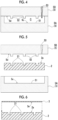
FIG. 2 is a schematic cross-sectional view of a mold for manufacturing the microchannel chip according to the present embodiment. -
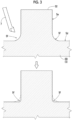
FIG. 3 is a schematic cross-sectional view showing one aspect of a process of manufacturing the mold for manufacturing the microchannel chip according to the present embodiment. -
FIG. 4 is a schematic cross-sectional view showing one aspect of a molding step for the microchannel chip according to the present embodiment. -
FIG. 5 is a schematic cross-sectional view showing one aspect of the molding step for the microchannel chip according to the present embodiment. -
FIG. 6 is a schematic cross-sectional view showing one aspect of an assembly step for the microchannel chip according to the present embodiment. - Hereinafter, an embodiment of the present invention will be described using the drawings. The embodiment to be described below is merely one example for facilitating understanding of the present invention, and does not limit the present invention. Namely, shapes, dimensions, disposition, and the like of members to be described below can be changed and improved without departing from the concept of the present invention, and the present invention includes equivalents thereof.
- In addition, in all the drawings, the same components are denoted by the same reference signs, and duplicate descriptions will be omitted as appropriate.
- A microchannel chip according to the present embodiment will be described with reference to the drawings. As shown in
FIG. 1 , amicrochannel chip 1 of the present embodiment includes aresin substrate 2 and a coveringmaterial 3 joined to theresin substrate 2. - As the resin forming the
resin substrate 2, a resin having excellent heat resistance and transparency can be appropriately selected. Theresin substrate 2 can be made of, for example, a resin selected from the group consisting of polycarbonate, a cycloolefin copolymer, a cycloolefin polymer, polymethylpentene, polystyrene, polymethyl (meth)acrylate, and polyethylene terephthalate. - The
resin substrate 2 includeschannel grooves 21 on one surface of the resin substrate 2 (in the present embodiment, ajoint surface 2a to the covering material 3). The number of thechannel grooves 21 may be one or plural. In a case where a plurality of thechannel grooves 21 are provided, thechannel grooves 21 may be provided in series or may be provided in parallel. In addition, thechannel groove 21 may include a branch. Thechannel grooves 21 may have, for example, a width of 1 mm or less and a depth of 0.01 mm or more and 0.5 mm or less. In this way, experiments and the like can be performed on a microscale. - The outer shape and size of the
resin substrate 2 can be appropriately set in consideration of handleability, analysis compatibility (compatibility with analysis methods and analysis devices), or the like. In the case of, for example, a quadrilateral shape (square shape or rectangular shape), for example, one side is preferably 10 mm or more and 200 mm or less and more preferably 10 mm or more and 150 mm or less. The outer shape of theresin substrate 2 may be other polygonal shapes, a circular shape, an elliptical shape, or the like. - The covering
material 3 can be formed of, for example, a resin film, a resin plate, or the like. As the resin forming the coveringmaterial 3, a resin having excellent heat resistance and transparency can be appropriately selected. The coveringmaterial 3 can be made of, for example, a resin selected from the group consisting of polycarbonate, a cycloolefin copolymer, a cycloolefin polymer, polymethylpentene, polystyrene, polymethyl (meth)acrylate, and polyethylene terephthalate. The resin forming the coveringmaterial 3 may be the same resin as the resin forming theresin substrate 2, or may be a different resin. - The thickness of the covering
material 3 is not particularly limited, and can be set to, for example, 0.01 mm or more and 1 mm or less. By setting the thickness to 0.01 mm or more, it becomes difficult for wrinkles or the like to occur during joining, and thechannel grooves 21 can be sufficiently sealed. In addition, by setting the thickness to 1 mm or less, excellent followability to irregularities of theresin substrate 2 can be obtained. - The
resin substrate 2 and the coveringmaterial 3 are laminated such that thejoint surface 2a of the resin substrate 2 (surface on which thechannel grooves 21 are formed) and ajoint surface 3a which is one surface of the coveringmaterial 3 are in contact with each other. The coveringmaterial 3 is joined to theresin substrate 2 to cover thechannel grooves 21. In this way, microchannels formed of thechannel grooves 21 are formed between theresin substrate 2 and the coveringmaterial 3. Themicrochannel chip 1 can be suitably used as, for example, a biochip such as a nucleic acid chip, a protein chip, an antibody chip, an aptamer chip, or a glycoprotein chip or a microanalysis chip for various chemical analyses. - The
microchannel chip 1 of the present embodiment is characterized in that in theresin substrate 2, a roundness of acorner 2c (refer toFIG. 1 ) formed at a boundary between thejoint surface 2a to the coveringmaterial 3 and aninner surface 2b defining eachchannel groove 21 is R5 µm or less. In a case where the roundness of thecorner 2c is more than R5 µm, when the coveringmaterial 3 is joined to theresin substrate 2, there is a possibility that a microspace remains at the portion of thecorner 2c, which causes bubbles to be generated in the channel. In this respect, by setting the roundness of thecorner 2c to R5 µm or less as in the present embodiment, theresin substrate 2 also including edges of thechannel grooves 21 and the coveringmaterial 3 can be firmly brought into close contact with each other when the coveringmaterial 3 is joined to theresin substrate 2. As a result, almost no microspace remains between theresin substrate 2 and the coveringmaterial 3, and in themicrochannel chip 1 finally obtained, it can be made difficult for bubbles to be generated in the channels. - The roundness of the
corner 2c at the boundary between thejoint surface 2a to the coveringmaterial 3 and theinner surface 2b defining eachchannel groove 21 is preferably R4.8 µm or less, more preferably R4.6 µm or less, and still more preferably R4.4 µm or less. According to this setting, it can be made more difficult for bubbles to be generated in the channels. - The
microchannel chip 1 of the present embodiment can be manufactured using amold 5 for injection molding and a hot press machine. For example, themicrochannel chip 1 can be manufactured by creating theresin substrate 2 using the mold 5 (molding step), and by thermally compressing theresin substrate 2 and the coveringmaterial 3 separately created using a hot press machine (assembly step). Themicrochannel chip 1 can also be manufactured by affixing together theresin substrate 2 and the coveringmaterial 3 using an adhesive, a pressure-sensitive adhesive, a pressure-sensitive adhesive film, or the like. - As shown in
FIG. 2 , themold 5 includes afirst mold 5A including a recessedportion 51 and asecond mold 5B includingridge portions 52. The recessedportion 51 corresponds to the outer shape of theresin substrate 2. Theridge portion 52 corresponds to the inner surface shape of thechannel groove 21. When thefirst mold 5A and thesecond mold 5B are mold-clamped, a cavity space C is formed as a space surrounded by an inner surface (firstinner surface 5c) of the recessedportion 51 and an inner surface (secondinner surface 5d) around portions of thesecond mold 5B at which theridge portions 52 are formed (refer toFIG. 4 ). Agate 53 communicating with the cavity space C is also formed in thesecond mold 5B. - In the present embodiment, as the
mold 5 used for the injection molding of theresin substrate 2, a mold formed by direct engraving instead of electroforming is used. The direct engraving is a processing method that creates a mold by cutting a metal block, and can be performed using, for example, a numerical control (NC) milling machine or the like. In themold 5 formed by such direct engraving (here, particularly, thesecond mold 5B including the ridge portions 52), as shown at the upper part ofFIG. 3 , normally, a roundness remains at acorner 5f between the secondinner surface 5d and anouter surface 5e of theridge portion 52 in thesecond mold 5B. The roundness of thecorner 5f is, for example, R10 µm or more, and typically, can be R20 µm or more. - In the present embodiment, in manufacturing the
mold 5, after normal direct engraving is performed, as shown inFIG. 3 , corner chamfering is further performed such that thecorner 5f between the secondinner surface 5d and theouter surface 5e of theridge portion 52 is close to a right angle. The corner chamfering can be performed using acornering tool 7. The roundness of thecorner 5f between the secondinner surface 5d and theouter surface 5e of theridge portion 52 is set to, for example, R5 µm or less by performing corner chamfering. The roundness of thecorner 5f is preferably set to R4.8 µm or less, more preferably R4.6 µm or less, and still more preferably R4.4 µm or less. - The
resin substrate 2 including thechannel grooves 21 on the one surface is formed by using themold 5 obtained in this way (molding step). In the molding step, as shown inFIG. 4 , thefirst mold 5A and thesecond mold 5B are mold-clamped, and the molten resin is injected from thegate 53 into the cavity space C formed therebetween. - The temperature of the
mold 5 used in the molding step is not particularly limited, and when the load deflection temperature of the resin material forming theresin substrate 2 under a high load (1.8 MPa) is T1 [°C], for example, the temperature of themold 5 is preferably (T1 - 20°C) or more and (T1°C) or less, more preferably (T1 - 15°C) or more and (T1°C) or less, and still more preferably (T1 - 10°C) or more and (T1°C) or less. According to this configuration, from the viewpoint of optimizing molding conditions related to the mold temperature, it can be made more difficult for bubbles to be generated. - The load deflection temperature can be measured in accordance with JIS K7191-1A method.
- When the temperature of the
mold 5 is less than the above-described lower limit value, there is a possibility that due to a rapid decrease in the temperature of the molten resin after injection, the fluidity of the molten resin decreases and the followability to themold 5 is impaired. On the other hand, when the temperature of themold 5 is greater than the above-described upper limit value, energy consumption increases and cooling also takes time, which may lead to a decrease in productivity. Therefore, theresin substrate 2 having a desired shape can be obtained with excellent productivity by setting the mold temperature within the above-described range. - The temperature of the molten resin injected into the
mold 5 in the molding step is not particularly limited, and when the glass transition temperature of the resin material forming theresin substrate 2 is Tg [°C], for example, the temperature of the molten resin is preferably (Tg + 130°C) or more and (Tg + 160°C) or less, more preferably (Tg + 130°C) or more and (Tg + 155°C) or less, and still more preferably (Tg + 130°C) or more and (Tg + 150°C) or less. According to this configuration, from the viewpoint of optimizing molding conditions related to the resin temperature, it can be made more difficult for bubbles to be generated. - When the temperature of the molten resin is less than the above-described lower limit value, there is a possibility that the fluidity is not sufficient and the followability to the
mold 5 is impaired. On the other hand, when the temperature of the molten resin is greater than the above-described upper limit value, the effect of improving the fluidity is limited even though energy consumption increases. Therefore, theresin substrate 2 having a desired shape can be obtained with excellent productivity by setting the resin temperature within the above-described range. - The injection pressure when the molten resin is injected into the
mold 5 in the molding step is not particularly limited, and for example, is preferably 90 MPa or more and 120 MPa or less, more preferably 95 MPa or more and 120 MPa or less, and still more preferably 100 MPa or more and 120 MPa or less. According to this configuration, from the viewpoint of optimizing molding conditions related to the injection pressure, it can be made more difficult for bubbles to be generated. - When the injection pressure of the molten resin is less than the above-described lower limit value, there is a possibility that the molten resin does not spread throughout the cavity space C and the followability to the
mold 5 is impaired. On the other hand, when the injection pressure of the molten resin is greater than the above-described upper limit value, the effect of improving the followability to themold 5 is limited even though energy consumption increases. Therefore, theresin substrate 2 having a desired shape can be obtained with excellent productivity by setting the injection pressure of the molten resin within the above-described range. - When the mold is opened after cooling, as shown in
FIG. 5 , theresin substrate 2 in which thechannel grooves 21, each having an outer shape corresponding to the recessedportion 51 of thefirst mold 5A and having an inner surface corresponding to theridge portion 52 of thesecond mold 5B, are formed on the one surface is obtained. At this time, since themold 5 subjected to corner chamfering in addition to normal direct engraving is used, theresin substrate 2 in which the roundness of thecorner 2c (refer toFIG. 1 ) formed at the boundary between thejoint surface 2a to the coveringmaterial 3 and theinner surface 2b defining eachchannel groove 21 is suppressed to R5 µm or less can be obtained. - Thereafter, the
resin substrate 2 obtained in the molding step and the coveringmaterial 3 separately created are laminated and joined together (assembly step). In the assembly step, first, as shown inFIG. 6 , the coveringmaterial 3 is laminated on theresin substrate 2 to cover thechannel grooves 21. Thereafter, the laminate is placed the laminate in a hot press machine, and theresin substrate 2 and the coveringmaterial 3 are joined together by thermocompression. The hot press machine includes a first block and a second block that sandwiches and compresses the laminate of theresin substrate 2 and the coveringmaterial 3 between the first block and the second block. Each of the first block and the second block includes a built-in heater. - As described above, in the
resin substrate 2 obtained in the molding step of the present embodiment, the roundness of thecorner 2c at the boundary between thejoint surface 2a and theinner surface 2b of eachchannel groove 21 is suppressed to R5 µm or less. For this reason, when theresin substrate 2 and the coveringmaterial 3 are joined together, theresin substrate 2 including the edges of thechannel grooves 21 and the coveringmaterial 3 firmly come into close contact with each other. Accordingly, almost no microspace remains between theresin substrate 2 and the covering material 3 (particularly, the portions of the edges of the channel grooves 21). Therefore, it can be made difficult for bubbles to be generated in the channels of themicrochannel chip 1. - The microchannel chip has been described above in detail by showing a specific embodiment; however, the present invention is not limited thereto. The embodiment disclosed in the present specification is provided as an example in all respects, and can be modified as appropriate without departing from the concept of the present disclosure.
- By forming the resin substrate including the channel grooves using the mold formed by direct engraving, it is possible to make it difficult for bubbles to be generated in the channels while manufacturing the microchannel chip at low cost.
-
- 1: Microchannel chip
- 2: Resin substrate
- 2a: Joint surface
- 2b: Inner surface
- 2c: Corner
- 3: Covering material
- 3a: Joint surface
- 5: Mold
- 5A: First mold
- 5B: Second mold
- 5c: First inner surface
- 5d: Second inner surface
- 5e: Outer surface
- 5f: Corner
- 21: Channel groove
- 51: Recessed portion
- 52: Ridge portion
- 53: Gate
- C: Cavity space
Claims (4)
- A microchannel chip comprising:a resin substrate manufactured using a mold formed by direct engraving, and including a channel groove on one surface of the resin substrate; anda covering material joined to the resin substrate to cover the channel groove,wherein in the resin substrate, a roundness of a corner formed at a boundary between a joint surface to the covering material and an inner surface defining the channel groove is R5 µm or less.
- The microchannel chip according to claim 1,
wherein when a load deflection temperature of a resin material forming the resin substrate is T1, the resin substrate is formed by injecting a molten resin into a cavity space formed in the mold heated to a temperature of (T1 - 20°C) or more and T1 or less. - The microchannel chip according to claim 1 or 2,
wherein when a glass transition temperature of a resin material forming the resin substrate is Tg, the resin substrate is formed by injecting a molten resin heated to a temperature of (Tg + 130°C) or more and (Tg + 160°C) or less into a cavity space formed in the mold. - The microchannel chip according to claim 1 or 2,
wherein the resin substrate is formed by injecting a molten resin into a cavity space formed in the mold at an injection pressure of 90 MPa or more and 120 MPa or less.
Applications Claiming Priority (2)
| Application Number | Priority Date | Filing Date | Title |
|---|---|---|---|
| JP2021141725 | 2021-08-31 | ||
| PCT/JP2022/032367 WO2023032896A1 (en) | 2021-08-31 | 2022-08-29 | Microchannel chip |
Publications (2)
| Publication Number | Publication Date |
|---|---|
| EP4397618A1 true EP4397618A1 (en) | 2024-07-10 |
| EP4397618A4 EP4397618A4 (en) | 2025-09-10 |
Family
ID=85412715
Family Applications (1)
| Application Number | Title | Priority Date | Filing Date |
|---|---|---|---|
| EP22864479.5A Withdrawn EP4397618A4 (en) | 2021-08-31 | 2022-08-29 | Microchannel chip |
Country Status (4)
| Country | Link |
|---|---|
| US (1) | US20240390891A1 (en) |
| EP (1) | EP4397618A4 (en) |
| JP (1) | JP7416331B2 (en) |
| WO (1) | WO2023032896A1 (en) |
Family Cites Families (9)
| Publication number | Priority date | Publication date | Assignee | Title |
|---|---|---|---|---|
| JPH07125206A (en) * | 1993-06-14 | 1995-05-16 | Ricoh Co Ltd | Thermal inkjet head |
| JP3921249B2 (en) * | 1995-08-21 | 2007-05-30 | リケンテクノス株式会社 | Embossed film manufacturing method and embossed film used for light diffusion film obtained thereby |
| JP2009019127A (en) * | 2007-07-12 | 2009-01-29 | Teijin Ltd | Optical disk substrate and optical disk |
| JP5944122B2 (en) * | 2011-07-22 | 2016-07-05 | アルバック成膜株式会社 | Microchannel substrate and manufacturing method thereof |
| JP2015199340A (en) | 2014-03-31 | 2015-11-12 | 住友ベークライト株式会社 | Method and apparatus for producing resinous micro-flow path device |
| US11000975B2 (en) * | 2016-10-13 | 2021-05-11 | Purdue Research Foundation | Methods of making hydrophobic contoured surfaces and hydrophobic contoured surfaces and devices made therefrom |
| JP2021099237A (en) * | 2019-12-20 | 2021-07-01 | 住友ベークライト株式会社 | Microchannel chip |
| JP2021109158A (en) * | 2020-01-14 | 2021-08-02 | 住友ベークライト株式会社 | Micro flow channel chip |
| JP6888898B1 (en) | 2020-03-05 | 2021-06-18 | ニシム電子工業株式会社 | Photovoltaic power control device |
-
2022
- 2022-08-29 EP EP22864479.5A patent/EP4397618A4/en not_active Withdrawn
- 2022-08-29 WO PCT/JP2022/032367 patent/WO2023032896A1/en not_active Ceased
- 2022-08-29 JP JP2023516501A patent/JP7416331B2/en active Active
- 2022-08-29 US US18/685,935 patent/US20240390891A1/en active Pending
Also Published As
| Publication number | Publication date |
|---|---|
| US20240390891A1 (en) | 2024-11-28 |
| EP4397618A4 (en) | 2025-09-10 |
| WO2023032896A1 (en) | 2023-03-09 |
| JPWO2023032896A1 (en) | 2023-03-09 |
| JP7416331B2 (en) | 2024-01-17 |
Similar Documents
| Publication | Publication Date | Title |
|---|---|---|
| CN105214747B (en) | Clamping-piece-type microfluidic device and manufacturing method | |
| KR100572207B1 (en) | Bonding method of plastic microchip | |
| EP3632563A1 (en) | Chip for sample detection and packaging method thereof | |
| EP3122487A1 (en) | Joining method | |
| JP2013164311A (en) | Fluid handing device and manufacturing method therefor | |
| US20110151198A1 (en) | Micro-Channel Chip and Manufacturing Method and Micro-Channel Chip | |
| EP2314436B1 (en) | Method for manufacturing micro-channel chip, die for molding micro-channel chip, and micro-channel chip | |
| CN104943139A (en) | Processing method of polymer micro-fluidic chip | |
| US20240390891A1 (en) | Microchannel chip | |
| TW587061B (en) | A method for manufacturing a polymer chip and an integrated mold for the same | |
| TW201922473A (en) | Microchip | |
| JP2013044528A (en) | Microchannel device | |
| JP2012007920A (en) | Manufacturing method of micro flow channel device | |
| JP2021109158A (en) | Micro flow channel chip | |
| JP2009166416A (en) | Method for manufacturing microchip, and microchip | |
| JP2019055379A (en) | Micro flow channel chip, and manufacturing method of the same | |
| JP2015199340A (en) | Method and apparatus for producing resinous micro-flow path device | |
| WO2009101845A1 (en) | Microchip and method for manufacturing the same | |
| JP6372254B2 (en) | Manufacturing method of microchannel chip | |
| JP2016083739A (en) | Microchip and method for manufacturing microchip | |
| JP2023035107A (en) | Micro flow channel chip and method for manufacturing the same | |
| EP3887118B1 (en) | Thermoplastic forming assemblage | |
| CN118106054B (en) | Segmented holding voltage bonding method for microfluidic chips and microfluidic chips | |
| JP2011123000A (en) | Component for microchannel chip, microchannel chip and analyzer | |
| JP2019042829A (en) | Method for manufacturing micro flow channel chip |
Legal Events
| Date | Code | Title | Description |
|---|---|---|---|
| STAA | Information on the status of an ep patent application or granted ep patent |
Free format text: STATUS: THE INTERNATIONAL PUBLICATION HAS BEEN MADE |
|
| PUAI | Public reference made under article 153(3) epc to a published international application that has entered the european phase |
Free format text: ORIGINAL CODE: 0009012 |
|
| STAA | Information on the status of an ep patent application or granted ep patent |
Free format text: STATUS: REQUEST FOR EXAMINATION WAS MADE |
|
| 17P | Request for examination filed |
Effective date: 20240223 |
|
| AK | Designated contracting states |
Kind code of ref document: A1 Designated state(s): AL AT BE BG CH CY CZ DE DK EE ES FI FR GB GR HR HU IE IS IT LI LT LU LV MC MK MT NL NO PL PT RO RS SE SI SK SM TR |
|
| DAV | Request for validation of the european patent (deleted) | ||
| DAX | Request for extension of the european patent (deleted) | ||
| A4 | Supplementary search report drawn up and despatched |
Effective date: 20250808 |
|
| RIC1 | Information provided on ipc code assigned before grant |
Ipc: B81B 1/00 20060101AFI20250804BHEP Ipc: B29C 33/38 20060101ALI20250804BHEP Ipc: B29C 45/26 20060101ALI20250804BHEP Ipc: G01N 37/00 20060101ALI20250804BHEP Ipc: B01L 3/00 20060101ALI20250804BHEP Ipc: B29C 33/42 20060101ALI20250804BHEP |
|
| STAA | Information on the status of an ep patent application or granted ep patent |
Free format text: STATUS: THE APPLICATION HAS BEEN WITHDRAWN |
|
| 18W | Application withdrawn |
Effective date: 20250924 |