EP4394884A2 - Transistor à diode source-drain intégrée - Google Patents
Transistor à diode source-drain intégrée Download PDFInfo
- Publication number
- EP4394884A2 EP4394884A2 EP23218249.3A EP23218249A EP4394884A2 EP 4394884 A2 EP4394884 A2 EP 4394884A2 EP 23218249 A EP23218249 A EP 23218249A EP 4394884 A2 EP4394884 A2 EP 4394884A2
- Authority
- EP
- European Patent Office
- Prior art keywords
- region
- gate
- anode
- trench
- electrode
- Prior art date
- Legal status (The legal status is an assumption and is not a legal conclusion. Google has not performed a legal analysis and makes no representation as to the accuracy of the status listed.)
- Pending
Links
Images




Classifications
-
- H—ELECTRICITY
- H10—SEMICONDUCTOR DEVICES; ELECTRIC SOLID-STATE DEVICES NOT OTHERWISE PROVIDED FOR
- H10D—INORGANIC ELECTRIC SEMICONDUCTOR DEVICES
- H10D30/00—Field-effect transistors [FET]
- H10D30/80—FETs having rectifying junction gate electrodes
- H10D30/83—FETs having PN junction gate electrodes
- H10D30/831—Vertical FETs having PN junction gate electrodes
-
- H—ELECTRICITY
- H10—SEMICONDUCTOR DEVICES; ELECTRIC SOLID-STATE DEVICES NOT OTHERWISE PROVIDED FOR
- H10D—INORGANIC ELECTRIC SEMICONDUCTOR DEVICES
- H10D30/00—Field-effect transistors [FET]
- H10D30/60—Insulated-gate field-effect transistors [IGFET]
- H10D30/611—Insulated-gate field-effect transistors [IGFET] having multiple independently-addressable gate electrodes influencing the same channel
- H10D30/615—Insulated-gate field-effect transistors [IGFET] having multiple independently-addressable gate electrodes influencing the same channel comprising a MOS gate electrode and at least one non-MOS gate electrode
-
- H—ELECTRICITY
- H10—SEMICONDUCTOR DEVICES; ELECTRIC SOLID-STATE DEVICES NOT OTHERWISE PROVIDED FOR
- H10D—INORGANIC ELECTRIC SEMICONDUCTOR DEVICES
- H10D30/00—Field-effect transistors [FET]
- H10D30/01—Manufacture or treatment
- H10D30/051—Manufacture or treatment of FETs having PN junction gates
-
- H—ELECTRICITY
- H10—SEMICONDUCTOR DEVICES; ELECTRIC SOLID-STATE DEVICES NOT OTHERWISE PROVIDED FOR
- H10D—INORGANIC ELECTRIC SEMICONDUCTOR DEVICES
- H10D62/00—Semiconductor bodies, or regions thereof, of devices having potential barriers
- H10D62/10—Shapes, relative sizes or dispositions of the regions of the semiconductor bodies; Shapes of the semiconductor bodies
- H10D62/17—Semiconductor regions connected to electrodes not carrying current to be rectified, amplified or switched, e.g. channel regions
- H10D62/213—Channel regions of field-effect devices
- H10D62/221—Channel regions of field-effect devices of FETs
- H10D62/235—Channel regions of field-effect devices of FETs of IGFETs
- H10D62/299—Channel regions of field-effect devices of FETs of IGFETs having lateral doping variations
- H10D62/307—Channel regions of field-effect devices of FETs of IGFETs having lateral doping variations the doping variations being parallel to the channel lengths
-
- H—ELECTRICITY
- H10—SEMICONDUCTOR DEVICES; ELECTRIC SOLID-STATE DEVICES NOT OTHERWISE PROVIDED FOR
- H10D—INORGANIC ELECTRIC SEMICONDUCTOR DEVICES
- H10D62/00—Semiconductor bodies, or regions thereof, of devices having potential barriers
- H10D62/10—Shapes, relative sizes or dispositions of the regions of the semiconductor bodies; Shapes of the semiconductor bodies
- H10D62/17—Semiconductor regions connected to electrodes not carrying current to be rectified, amplified or switched, e.g. channel regions
- H10D62/213—Channel regions of field-effect devices
- H10D62/221—Channel regions of field-effect devices of FETs
- H10D62/328—Channel regions of field-effect devices of FETs having PN junction gates
-
- H—ELECTRICITY
- H10—SEMICONDUCTOR DEVICES; ELECTRIC SOLID-STATE DEVICES NOT OTHERWISE PROVIDED FOR
- H10D—INORGANIC ELECTRIC SEMICONDUCTOR DEVICES
- H10D62/00—Semiconductor bodies, or regions thereof, of devices having potential barriers
- H10D62/10—Shapes, relative sizes or dispositions of the regions of the semiconductor bodies; Shapes of the semiconductor bodies
- H10D62/17—Semiconductor regions connected to electrodes not carrying current to be rectified, amplified or switched, e.g. channel regions
- H10D62/343—Gate regions of field-effect devices having PN junction gates
-
- H—ELECTRICITY
- H10—SEMICONDUCTOR DEVICES; ELECTRIC SOLID-STATE DEVICES NOT OTHERWISE PROVIDED FOR
- H10D—INORGANIC ELECTRIC SEMICONDUCTOR DEVICES
- H10D62/00—Semiconductor bodies, or regions thereof, of devices having potential barriers
- H10D62/10—Shapes, relative sizes or dispositions of the regions of the semiconductor bodies; Shapes of the semiconductor bodies
- H10D62/17—Semiconductor regions connected to electrodes not carrying current to be rectified, amplified or switched, e.g. channel regions
- H10D62/393—Body regions of DMOS transistors or IGBTs
-
- H—ELECTRICITY
- H10—SEMICONDUCTOR DEVICES; ELECTRIC SOLID-STATE DEVICES NOT OTHERWISE PROVIDED FOR
- H10D—INORGANIC ELECTRIC SEMICONDUCTOR DEVICES
- H10D62/00—Semiconductor bodies, or regions thereof, of devices having potential barriers
- H10D62/80—Semiconductor bodies, or regions thereof, of devices having potential barriers characterised by the materials
- H10D62/83—Semiconductor bodies, or regions thereof, of devices having potential barriers characterised by the materials being Group IV materials, e.g. B-doped Si or undoped Ge
- H10D62/832—Semiconductor bodies, or regions thereof, of devices having potential barriers characterised by the materials being Group IV materials, e.g. B-doped Si or undoped Ge being Group IV materials comprising two or more elements, e.g. SiGe
- H10D62/8325—Silicon carbide
-
- H—ELECTRICITY
- H10—SEMICONDUCTOR DEVICES; ELECTRIC SOLID-STATE DEVICES NOT OTHERWISE PROVIDED FOR
- H10D—INORGANIC ELECTRIC SEMICONDUCTOR DEVICES
- H10D64/00—Electrodes of devices having potential barriers
- H10D64/20—Electrodes characterised by their shapes, relative sizes or dispositions
- H10D64/27—Electrodes not carrying the current to be rectified, amplified, oscillated or switched, e.g. gates
- H10D64/311—Gate electrodes for field-effect devices
- H10D64/411—Gate electrodes for field-effect devices for FETs
- H10D64/511—Gate electrodes for field-effect devices for FETs for IGFETs
- H10D64/512—Disposition of the gate electrodes, e.g. buried gates
- H10D64/513—Disposition of the gate electrodes, e.g. buried gates within recesses in the substrate, e.g. trench gates, groove gates or buried gates
-
- H—ELECTRICITY
- H10—SEMICONDUCTOR DEVICES; ELECTRIC SOLID-STATE DEVICES NOT OTHERWISE PROVIDED FOR
- H10D—INORGANIC ELECTRIC SEMICONDUCTOR DEVICES
- H10D62/00—Semiconductor bodies, or regions thereof, of devices having potential barriers
- H10D62/10—Shapes, relative sizes or dispositions of the regions of the semiconductor bodies; Shapes of the semiconductor bodies
- H10D62/117—Shapes of semiconductor bodies
-
- H—ELECTRICITY
- H10—SEMICONDUCTOR DEVICES; ELECTRIC SOLID-STATE DEVICES NOT OTHERWISE PROVIDED FOR
- H10D—INORGANIC ELECTRIC SEMICONDUCTOR DEVICES
- H10D62/00—Semiconductor bodies, or regions thereof, of devices having potential barriers
- H10D62/10—Shapes, relative sizes or dispositions of the regions of the semiconductor bodies; Shapes of the semiconductor bodies
- H10D62/124—Shapes, relative sizes or dispositions of the regions of semiconductor bodies or of junctions between the regions
- H10D62/126—Top-view geometrical layouts of the regions or the junctions
- H10D62/127—Top-view geometrical layouts of the regions or the junctions of cellular field-effect devices, e.g. multicellular DMOS transistors or IGBTs
Definitions
- a reverse current (also referred to as source-drain current or 3rd quadrant current) conduction path does not exist, and current flow between drain and source approaches zero during their operation in the off-state.
- Such feature namely having a bi-directional current flow or providing a 3rd quadrant current-conduction path with a reduced source-drain voltage (V SD ) drop, may be utilized in power converter topologies and applications.
- the semiconductor structure further comprises a first source electrode over the first source region and between the first gate trench and the anode trench, a first gate electrode over a portion of a bottom surface of the first gate trench, and an anode electrode over a portion of a bottom of the anode trench, wherein the first source electrode and the anode electrode are electrically coupled, the first gate region forms part of a first vertical junction field-effect transistor (JFET) cell, and the anode region forms part of a vertical diode cell, which is coupled anti-parallel with the first vertical JFET cell.
- the substrate and the body region may comprise silicon carbide.
- the first gate region and the anode region may be doped with a p-type dopant and a remaining portion of the body region and the substrate may be doped with an n-type dopant.
- the first source electrode and the anode electrode may integrally form part of a continuous electrode structure that covers at least a portion of the first source region, a portion of a first side wall of the anode trench, and a portion of the bottom of the anode trench.
- the first source electrode and the anode electrode integrally form part of a continuous electrode structure that covers at least a portion of the first source region, a first side wall of the anode trench, and the bottom of the anode trench.
- the semiconductor structure further comprises a first source electrode over the first source region and between the first gate trench and the anode trench, a first gate electrode over a portion of a bottom surface of the first gate trench, an anode electrode over a portion of a bottom of the anode trench, wherein the first source electrode and the anode electrode are electrically coupled, the first gate region forms part of a first vertical junction field-effect transistor (JFET) cell, and the anode region forms part of a vertical diode cell, which is coupled anti-parallel with the first vertical JFET cell.
- JFET vertical junction field-effect transistor
- the device structure further comprises a metal oxide semiconductor field-effect transistor (MOSFET) comprising a gate electrode, a source electrode, and a drain electrode, wherein the drain electrode of the MOSFET is coupled in series to the first source electrode of the first vertical JFET cell coupled anti-parallel with the vertical diode cell, forming a dual-gate cascode FET device.
- MOSFET metal oxide semiconductor field-effect transistor
- the semiconductor structure further comprises a second source region extending into the body region from the top surface, a second U-shaped gate region having a portion below the second source region and defining a second gate trench, wherein the anode region has a second portion below the second source region such that the anode trench is between the first gate trench and the second gate trench, a second source electrode over the second source region and between the second gate trench and the anode trench, a second gate electrode over a portion of a bottom surface of the second gate trench, wherein the first source electrode, the second source electrode, and the anode electrode are electrically coupled, and wherein the second gate region forms part of a second vertical JFET cell located on the opposite side of the first vertical JFET cell from the vertical diode cell, and the vertical diode cell is coupled anti-parallel with the first vertical JFET cell and the second vertical JFET cell.
- a method of fabricating a semiconductor structure comprises providing a drain-cathode electrode, providing a substrate over the drain-cathode electrode, providing a body region over the substrate wherein the body region comprises a top surface, a first source region extending into the body region from the top surface, a first U-shaped gate region having a portion below the first source region and defining a first gate trench, and a U-shaped anode region having a first portion below the first source region and defining an anode trench.
- the method further comprises providing a first source electrode over the first source region and between the first gate trench and the anode trench, providing a first gate electrode over a portion of a bottom surface of the first gate trench, providing an anode electrode over a portion of a bottom of the anode trench, and electrically coupling the first source electrode and the anode electrode such that the first gate region forms part of a first vertical junction field-effect transistor (JFET) cell, and the anode region forms part of a vertical diode cell, which is coupled anti-parallel with the first vertical JFET cell.
- JFET vertical junction field-effect transistor
- any of the foregoing aspects individually or together, and/or various separate aspects and features as described herein, may be combined for additional advantage. Any of the various features and elements as disclosed herein may be combined with one or more other disclosed features and elements unless indicated to the contrary herein.
- Embodiments are described herein with reference to schematic illustrations of embodiments of the disclosure. As such, the actual dimensions of the layers and elements can be different, and variations from the shapes of the illustrations as a result, for example, of manufacturing techniques and/or tolerances, are expected. For example, a region illustrated or described as square or rectangular can have rounded or curved features, and regions shown as straight lines may have some irregularity. Thus, the regions illustrated in the figures are schematic and their shapes are not intended to illustrate the precise shape of a region of a device and are not intended to limit the scope of the disclosure. Additionally, sizes of structures or regions may be exaggerated relative to other structures or regions for illustrative purposes and, thus, are provided to illustrate the general structures of the present subject matter and may or may not be drawn to scale. Common elements between figures may be shown herein with common element numbers and may not be subsequently
- cascode structure reduces the on-state resistance by driving the VJFET into positive V GS values and provides an improved control of switching characteristics by enabling the gate of the VJFET device to be directly driven
- cascode structures utilized in hard switching applications experience excessive 3rd quadrant energy losses due to the 3rd quadrant current (I SD ) flowing through the VJFET channel region and the source-drain voltage (V SD ) exceeding the absolute value of VJFET's threshold voltage (V th ).
- Embodiments of the present disclosure provide VJFETs monolithically integrated with anti-parallel PN diodes. These structures can be applied to a variety of semiconductor devices including but not limited to other types of transistors and diodes and to other e-channel and p-channel JFET structures.
- a normally-off operation mode can be implemented by connecting the normally-on VJFET with an anti-parallel diode structure to a low-voltage MOSFET in a cascode configuration.
- FIG. 1A illustrates a cross-sectional view of an embodiment of depletion-mode trench gate vertical JFETs (VJFETs) with integrated source-drain anti-parallel diodes (herein after referred to as "VJFET-diode structure 100 ") which are built on a wafer comprising a substrate 10 and a body region 12, both of which are doped with an n-type dopant.
- VJFET-diode structure 100 integrated source-drain anti-parallel diodes
- bottom and sidewalls surrounding each of the first gate trench 16a, the second gate trench 16b, and the anode trench 14 are doped with a p-type dopant to form a first gate region 20a, a second gate region 20b, and an anode region 22, respectively, such that the first gate region 20a forms a U-shaped region under the source region 24 that defines the first gate trench 16a with a first portion of the U-shaped region under the first source region 24a.
- the anode region 22 forms a U-shaped region under the source region 24 to define the anode trench 14 with a first portion of the U-shaped region under the first source region 24a.
- a first channel region 18a and a second channel region 18b form part of the body region 12.
- the first channel region 18a extends vertically into the body region 12 from below the first source region 24a and forms laterally in between the first gate region 20a and the anode region 22.
- the second channel region 18b extends vertically into the body region 12 below the second source region 24b and forms laterally in between the anode region 22 and the second gate region 20b. It should be noted that while only two channel regions are shown in FIG. 1A , the structures illustrated may be replicated many times to form a plurality of channel regions in a semiconductor device designed according to disclosures of the present application.
- the anode electrode 28, the anode region 22, and the drain-cathode electrode 32 form part of a vertical diode cell 40.
- the first source electrode 26a and the first source region 24a along with the drain-cathode electrode 32, the first gate electrode 30a, and the first gate region 20a form part of a first VJFET cell 36.
- the second source electrode 26b and the second source region 24b along with the drain-cathode electrode 32, the second gate electrode 30b, and the second gate region 20b form part of a second VJFET cell 38, which is located on the opposite side of the first VJFET cell 36 from the vertical diode cell 40, and the vertical diode cell 40 is coupled anti-parallel with the first VJFET cell 36 and the second VJFET cell 38.
- a single unit cell 200 as shown in the embodiment of FIG. 1A includes portions of the first VJFET cell 36 and portions of the vertical diode cell 40 adjacent to it.
- the integration of the source-drain anti-parallel diode into the depletion-mode trench VJFET semiconductor structure allows a 3rd quadrant current conduction while the VJFET is in off-state with a significant reduction of saturation current density (J sat ) and maintaining a similar threshold voltage (V th ) and specific on-resistance (R ds A).
- FIG. 1B shows a cross-sectional view of an embodiment of depletion-mode trench gate VJFET with integrated source-drain anti-parallel diodes (herein after referred to as "VJFET-diode structure 100 ").
- the body region 12 may further comprise an n-type drift layer 42 configured to withstand a desired blocking voltage.
- the drift layer 42 may form above the substrate 10 and have a doping level in the range of 2e14cm -3 to 5e16cm -3 .
- the doping level of the body region 12 may be in the ranges of 2e14cm -3 to 1e17cm -3
- the doping level of the substrate 10 may be in the range of 2e17cm -3 to 1e19cm -3 .
- the body region 12 comprises channel regions 18 including the first channel region 18a and the second channel region 18b.
- the first channel region 18a forms below the first source region 24a and between the first gate region 20a and the anode region 22.
- the second channel region 18b forms below the second source region 24b and between the second gate region 20b and the anode region 22.
- the doping level of the channel regions 18, including the first channel region 18a and the second channel region 18b may be at least two times lower than the lowest doping concentration in the rest of the body region 12 and in the range of 1e14cm -3 to 2e16cm -3 .
- a heavily doped N-type buffer layer may form over a top surface of the substrate 10 by means of epitaxial growth. It is further noted that while the body region 12, the substrate 10, the first channel region 18a, and the second channel region 18b, buffer, the current spreading layer 44, and source regions 24 including the first source region 24a and the second source region 24b are depicted to have had been doped with an n-type dopant, and while a gate region 20 and the anode region 22 are shown with a p-type dopant, in practice, the doping types can be switched among these same structures.
- the first source electrode 26a and the anode electrode 28 integrally form part of a continuous electrode structure 26' that covers over at least a portion of the first source region 24a to provide the first source electrode 26a, a portion of a first side wall of the anode region 22 adjacent to the first source electrode 26a to form a first sidewall electrode 26d, and a portion of the bottom of anode trench 14 to form a bottom surface (anode) electrode 26c.
- the first source electrode 26a and the anode electrode 28 integrally form part of the continuous electrode structure 26' that covers over at least a portion of the first source region 24a to provide the first source electrode 26a, the first side wall of the anode region 22 adjacent to the first source electrode 26a to form the first sidewall electrode 26d, and the bottom of anode trench 14 to form the bottom surface (anode) electrode 26c.
- the first source electrode 26a, the second source electrode 26b, and the anode electrode 28 may integrally form part of a continuous electrode structure 26' that covers at least a portion of the first source region 24a to provide the first source electrode 26a, a portion of the first side wall of the anode region 22 adjacent to the first source electrode 26a to form the first sidewall electrode 26d, a portion of the bottom of anode trench 14 to form the bottom surface (anode) electrode 26c, a portion of the second side wall of the anode region 22 adjacent to the second source electrode 26b to form the second sidewall electrode 26e, and at least a portion of the second source region 24b to provide the second source electrode 26b.
- first source electrode 26a, the second source electrode 26b, and the anode electrode 28 integrally form part of a continuous electrode structure 26' that covers at least a portion of the first source region 24a to provide the first source electrode 26a, the first side wall of the anode region 22 adjacent to the first source electrode 26a to form the first sidewall electrode 26d, the bottom of anode trench 14 to form the bottom surface (anode) electrode 26c, the second side wall of the anode region 22 adjacent to the second source electrode 26b to form a second sidewall electrode 26e, and at least a portion of the second source region 24b to provide the second source electrode 26b.
- a mostly self-aligned silicidation (salicidation) process may be used to form a separated first and second gate electrodes 30a and 30b, a continuous electrode structure 26' that couples the first source electrode 26a of the first VJFET cell 36 with the bottom surface (anode) electrode 26c of the vertical diode cell 40 and the second source electrode 26b of the second VJFET cell 38.
- the source metal for silicidation process may include, but not limited to, nickel and titanium.
- a drain-cathode electrode 32 may be formed by a combination of metal deposition and laser irradiation.
- a second metal overlay 52 is deposited at least partially over the backside of the drain-cathode electrode 32.
- Multiple metallization layers including one or more of Ni, Ti, TiW, TiN, W, Pd, Au, and silver (Ag) may comprise the second metal overlay 52.
- Basal plane defect (BPD) and stacking fault screening has to be implemented on starting an epitaxial wafer and at device level in the same manner as it is implemented in silicon carbide MOSFETs with built-in source-drain diode.
- FIG. 2 shows an dual-gate cascode FET configuration 300 comprising a plurality of alternating trench VJFET cells and anti-parallel source-drain diode cells (herein after referred to as "VJFET/diode structure 100′′′ ) connected in series with a MOSFET 70.
- the VJFET/diode structure 100' comprises a unified drain electrode 52', a unified gate electrode 30', and a unified source electrode 50'.
- the MOSFET 70 may be a low-voltage transistor having a MOSFET drain electrode 72, a MOSFET gate electrode 74, and a MOSFET source electrode 76.
- the integration of an anti-parallel source-drain diode within a trench VJFET structure to form the single unit cell 200 reduces the gate-drain capacitance C GD 58 by approximately 50% to a first gate-drain capacitance C GD 58a and by eliminating a second gate-drain capacitance C GD 58b.
- the integration of an anti-parallel source-drain diode within a trench VJFET structure to form the single unit cell 200 reduces the gate-source capacitance C GS 60 by approximately 50% to a first gate-source capacitance C GS 60a and by eliminating a second gate-source capacitance C GS 60b.
- FIG. 4 depicts the electron flow lines (forward current flow is in the opposite direction) through a single unit cell 200 embodiment as illustrated schematically with electron flow lines.
- forward current flow occurs through both the VJFET side of the cell 54 and the anti-parallel diode side of the cell 56.
- the forward current through the VJFET side of the cell 54 as illustrated schematically with VJFET current flow lines 62 and the forward current through the diode side of the cell 56 as illustrated schematically with diode current flow lines 64 illustrate the minimal impact of integrating a source-drain anti-parallel diode within the device structure as forward current continues to spread efficiently through the entire structure.
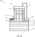
- FIGS. 5A-5C depict embodiments of a first single unit cell 400, a second single unit cell 500, and a third single unit cell 550, respectively, each having one or more secondary vertical channel regions 66.
- the one or more secondary vertical channel regions 66 as shown in FIGS. 5A and 5C may be formed either by angled ion implantation or by vertical ion implantation or a combination of both.
- FIG. 5B illustrates an embodiment of a secondary vertical channel region 66, wherein the secondary vertical channel region 66 runs alongside the center of the channel region 18.
- the secondary vertical channel region 66 as shown in FIG. 5B has a maximum doping level that is at least 50% higher than a minimum doping level of the channel region 18.
- FIG. 5C illustrates an embodiment of a secondary vertical region 66, wherein the secondary vertical channel region 66 runs along the sidewall of the channel region 18 that is one the side of the gate electrode 30 but there is no secondary vertical region 66 on the sidewall on the side of the anode 28.
- the process of manufacturing the third single unit cell 550 is simplified since secondary vertical channel region 66 only has to be implemented on one sidewall.
- the benefit of having another secondary vertical channel region 66 along the side of the body like the first single unit cell 400 may be limited since the gate electrode 30 will primarily affect the operation of the adjacent secondary vertical channel in both forward conduction and off-state blocking..
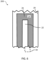
- FIG. 6 is a perspective top view layout of a single unit cell embodiment 200 as shown in FIG. 3 .
- multiple single unit cells may be connected in parallel with the alternating gate regions 20 and the anode regions 22.
- the anode region 22 is surrounded by the source region 24 mesa and the source region mesa 24 is itself surrounded by the gate region 20.
- the electrical coupling 34 is used to electrically connect the anode electrode (not shown) to the source electrode 26 that is disposed over a top surface of the source region 24.
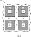
- FIG. 7 is a perspective top view layout of altering depletion-mode trench gate vertical JFETs with an integrated source-drain anti-parallel diodes 600.
- the cell layout comprises the anode region 22 of multiple diode cells that are fully surrounded by source mesas (not shown) having the source electrode 26 over their top surfaces.
- the gate regions 20 form a grid pattern between the isolated anode regions 22 surrounded by source region 24 mesas covered with the source electrodes 26.
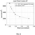
- the curve chart of FIG. 8 shows that compared with the baseline obtained from a conventional trench VJFET design with no integrated source-drain diode, the integration of a source-drain anti-parallel diode reduces J sat values by approximately 50% with minimal impact (approximately 20% increase) on R DS A.
- the substantial reduction of J sat may significantly improve the short-circuit withstand time, allowing for more time for protective circuitry to shut-off the gate of the VJFET in case of a short-circuit event.
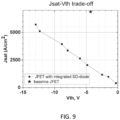
- the curve chart of FIG. 9 further illustrates that compared with the baseline obtained from a conventional trench VJFET design with no integrated source-drain diode, the integration of a source-drain anti-parallel diode into a trench VJFET structure allows for a significant reduction of saturation current density (J sat ) with minimal impact on the threshold voltage (V th ).
- FIG. 10 shows a modeled curve chart of gate-source breakdown voltage (BV GS ) versus the threshold voltage (V th ) for the single unit cell 200 embodiment of a trench VJFET with an integrated anti-parallel source-drain as shown in FIG. 3 .
- V GS gate-source breakdown voltage
- V th threshold voltage
- VJFETs vertical junction field-effect transistors
- MOSFET metal oxide semiconductor field-effect transistor
Landscapes
- Junction Field-Effect Transistors (AREA)
- Metal-Oxide And Bipolar Metal-Oxide Semiconductor Integrated Circuits (AREA)
Applications Claiming Priority (2)
| Application Number | Priority Date | Filing Date | Title |
|---|---|---|---|
| US202263477724P | 2022-12-29 | 2022-12-29 | |
| US18/533,355 US20240222504A1 (en) | 2022-12-29 | 2023-12-08 | Transistor with integrated source-drain diode |
Publications (2)
| Publication Number | Publication Date |
|---|---|
| EP4394884A2 true EP4394884A2 (fr) | 2024-07-03 |
| EP4394884A3 EP4394884A3 (fr) | 2025-01-08 |
Family
ID=89224193
Family Applications (1)
| Application Number | Title | Priority Date | Filing Date |
|---|---|---|---|
| EP23218249.3A Pending EP4394884A3 (fr) | 2022-12-29 | 2023-12-19 | Transistor à diode source-drain intégrée |
Country Status (2)
| Country | Link |
|---|---|
| US (1) | US20240222504A1 (fr) |
| EP (1) | EP4394884A3 (fr) |
Families Citing this family (3)
| Publication number | Priority date | Publication date | Assignee | Title |
|---|---|---|---|---|
| US11502667B2 (en) | 2019-01-14 | 2022-11-15 | Qorvo Us, Inc. | Top electrodes with step arrangements for bulk acoustic wave resonators |
| DE102024206949A1 (de) | 2024-07-24 | 2026-01-29 | Robert Bosch Gesellschaft mit beschränkter Haftung | Verfahren zur Herstellung eines Halbleiterbauelements und Halbleiterbauelement |
| CN119069534B (zh) * | 2024-11-04 | 2025-04-29 | 苏州龙驰半导体科技有限公司 | 沟槽型电容耦合栅控结型场效应晶体管 |
Family Cites Families (5)
| Publication number | Priority date | Publication date | Assignee | Title |
|---|---|---|---|---|
| JP4719472B2 (ja) * | 2005-01-06 | 2011-07-06 | 株式会社日立製作所 | シリコンカーバイド静電誘導トランジスタ |
| US7763506B2 (en) * | 2007-09-10 | 2010-07-27 | Infineon Technologies Austria Ag | Method for making an integrated circuit including vertical junction field effect transistors |
| JP2010147405A (ja) * | 2008-12-22 | 2010-07-01 | Renesas Technology Corp | 半導体装置およびその製造方法 |
| JP7118050B2 (ja) * | 2016-09-09 | 2022-08-15 | ユナイテッド シリコン カーバイド、インク. | 改善された閾値電圧制御を有するトレンチ垂直jfet |
| WO2018132458A1 (fr) * | 2017-01-13 | 2018-07-19 | United Silicon Carbide, Inc. | Jfet vertical à tranchées avec terminaison d'échelle |
-
2023
- 2023-12-08 US US18/533,355 patent/US20240222504A1/en active Pending
- 2023-12-19 EP EP23218249.3A patent/EP4394884A3/fr active Pending
Also Published As
| Publication number | Publication date |
|---|---|
| US20240222504A1 (en) | 2024-07-04 |
| EP4394884A3 (fr) | 2025-01-08 |
Similar Documents
| Publication | Publication Date | Title |
|---|---|---|
| US11177354B2 (en) | Method of manufacturing silicon carbide semiconductor devices | |
| US10522672B2 (en) | Semiconductor device | |
| EP4394884A2 (fr) | Transistor à diode source-drain intégrée | |
| EP2165367B1 (fr) | Transistors à commutation de puissance perfectionnés | |
| EP1396030B1 (fr) | Dispositif semi-conducteur de puissance vertical et sa méthode de fabrication | |
| US8829573B2 (en) | Semiconductor devices with minimized current flow differences and methods of same | |
| US20140264477A1 (en) | Vjfet devices | |
| US20090014719A1 (en) | Semiconductor device with large blocking voltage | |
| US9825025B2 (en) | Semiconductor device and method of manufacturing semiconductor device | |
| JP7182599B2 (ja) | 半導体装置及びパワーモジュール | |
| US9029874B2 (en) | Semiconductor device having a first silicon carbide semiconductor layer and a second silicon carbide semiconductor layer | |
| JP6740798B2 (ja) | 半導体装置及び半導体装置の製造方法 | |
| CN108886038A (zh) | 半导体装置 | |
| US20220285485A1 (en) | Schottky barrier diode and method for manufacturing the same | |
| CN118280987A (zh) | 具有集成源极-漏极二极管的晶体管 | |
| US12446300B2 (en) | Semiconductor devices having on-chip gate resistors | |
| US20250294865A1 (en) | Semiconductor devices having intrinsic gate-to-drain capacitances that are only partly in series with a gate resistor | |
| US20250338571A1 (en) | Trench gate wide bandgap junction field effect transistors with termination regions having planar upper surfaces | |
| US12382678B2 (en) | Transistor arrangement with a lateral superjunction transistor device | |
| US20260052738A1 (en) | Power semiconductor devices and methods of forming the same | |
| US20240421151A1 (en) | Vertical junction field-effect transistors with source-drain diode cells integrated at die level | |
| EP4428927B1 (fr) | Transistor multicanal à haute mobilité d'électrons avec capacité d'entrée réduite | |
| US12477800B2 (en) | Semiconductor diode and manufacturing method | |
| US11682696B2 (en) | Semiconductor device having a high breakdown voltage |
Legal Events
| Date | Code | Title | Description |
|---|---|---|---|
| PUAI | Public reference made under article 153(3) epc to a published international application that has entered the european phase |
Free format text: ORIGINAL CODE: 0009012 |
|
| STAA | Information on the status of an ep patent application or granted ep patent |
Free format text: STATUS: THE APPLICATION HAS BEEN PUBLISHED |
|
| AK | Designated contracting states |
Kind code of ref document: A2 Designated state(s): AL AT BE BG CH CY CZ DE DK EE ES FI FR GB GR HR HU IE IS IT LI LT LU LV MC ME MK MT NL NO PL PT RO RS SE SI SK SM TR |
|
| RIC1 | Information provided on ipc code assigned before grant |
Ipc: H01L 29/06 20060101ALN20240916BHEP Ipc: H01L 29/808 20060101ALI20240916BHEP Ipc: H01L 29/10 20060101AFI20240916BHEP |
|
| PUAL | Search report despatched |
Free format text: ORIGINAL CODE: 0009013 |
|
| AK | Designated contracting states |
Kind code of ref document: A3 Designated state(s): AL AT BE BG CH CY CZ DE DK EE ES FI FR GB GR HR HU IE IS IT LI LT LU LV MC ME MK MT NL NO PL PT RO RS SE SI SK SM TR |
|
| RIC1 | Information provided on ipc code assigned before grant |
Ipc: H01L 29/06 20060101ALN20241205BHEP Ipc: H01L 29/808 20060101ALI20241205BHEP Ipc: H01L 29/10 20060101AFI20241205BHEP |
|
| RAP1 | Party data changed (applicant data changed or rights of an application transferred) |
Owner name: UNITED SILICON CARBIDE INC. |
|
| STAA | Information on the status of an ep patent application or granted ep patent |
Free format text: STATUS: REQUEST FOR EXAMINATION WAS MADE |
|
| 17P | Request for examination filed |
Effective date: 20250704 |
|
| P01 | Opt-out of the competence of the unified patent court (upc) registered |
Free format text: CASE NUMBER: UPC_APP_0682_4394884/2025 Effective date: 20250721 |
|
| RAP3 | Party data changed (applicant data changed or rights of an application transferred) |
Owner name: UNITED SILICON CARBIDE INC. |
|
| P02 | Opt-out of the competence of the unified patent court (upc) changed |
Free format text: CASE NUMBER: UPC_APP_1096_4394884/2025 Effective date: 20250725 |