EP4394884A2 - Transistor with integrated source-drain diode - Google Patents
Transistor with integrated source-drain diode Download PDFInfo
- Publication number
- EP4394884A2 EP4394884A2 EP23218249.3A EP23218249A EP4394884A2 EP 4394884 A2 EP4394884 A2 EP 4394884A2 EP 23218249 A EP23218249 A EP 23218249A EP 4394884 A2 EP4394884 A2 EP 4394884A2
- Authority
- EP
- European Patent Office
- Prior art keywords
- region
- gate
- anode
- trench
- electrode
- Prior art date
- Legal status (The legal status is an assumption and is not a legal conclusion. Google has not performed a legal analysis and makes no representation as to the accuracy of the status listed.)
- Pending
Links
Images




Classifications
-
- H—ELECTRICITY
- H10—SEMICONDUCTOR DEVICES; ELECTRIC SOLID-STATE DEVICES NOT OTHERWISE PROVIDED FOR
- H10D—INORGANIC ELECTRIC SEMICONDUCTOR DEVICES
- H10D30/00—Field-effect transistors [FET]
- H10D30/80—FETs having rectifying junction gate electrodes
- H10D30/83—FETs having PN junction gate electrodes
- H10D30/831—Vertical FETs having PN junction gate electrodes
-
- H—ELECTRICITY
- H10—SEMICONDUCTOR DEVICES; ELECTRIC SOLID-STATE DEVICES NOT OTHERWISE PROVIDED FOR
- H10D—INORGANIC ELECTRIC SEMICONDUCTOR DEVICES
- H10D30/00—Field-effect transistors [FET]
- H10D30/60—Insulated-gate field-effect transistors [IGFET]
- H10D30/611—Insulated-gate field-effect transistors [IGFET] having multiple independently-addressable gate electrodes influencing the same channel
- H10D30/615—Insulated-gate field-effect transistors [IGFET] having multiple independently-addressable gate electrodes influencing the same channel comprising a MOS gate electrode and at least one non-MOS gate electrode
-
- H—ELECTRICITY
- H10—SEMICONDUCTOR DEVICES; ELECTRIC SOLID-STATE DEVICES NOT OTHERWISE PROVIDED FOR
- H10D—INORGANIC ELECTRIC SEMICONDUCTOR DEVICES
- H10D30/00—Field-effect transistors [FET]
- H10D30/01—Manufacture or treatment
- H10D30/051—Manufacture or treatment of FETs having PN junction gates
-
- H—ELECTRICITY
- H10—SEMICONDUCTOR DEVICES; ELECTRIC SOLID-STATE DEVICES NOT OTHERWISE PROVIDED FOR
- H10D—INORGANIC ELECTRIC SEMICONDUCTOR DEVICES
- H10D62/00—Semiconductor bodies, or regions thereof, of devices having potential barriers
- H10D62/10—Shapes, relative sizes or dispositions of the regions of the semiconductor bodies; Shapes of the semiconductor bodies
- H10D62/17—Semiconductor regions connected to electrodes not carrying current to be rectified, amplified or switched, e.g. channel regions
- H10D62/213—Channel regions of field-effect devices
- H10D62/221—Channel regions of field-effect devices of FETs
- H10D62/235—Channel regions of field-effect devices of FETs of IGFETs
- H10D62/299—Channel regions of field-effect devices of FETs of IGFETs having lateral doping variations
- H10D62/307—Channel regions of field-effect devices of FETs of IGFETs having lateral doping variations the doping variations being parallel to the channel lengths
-
- H—ELECTRICITY
- H10—SEMICONDUCTOR DEVICES; ELECTRIC SOLID-STATE DEVICES NOT OTHERWISE PROVIDED FOR
- H10D—INORGANIC ELECTRIC SEMICONDUCTOR DEVICES
- H10D62/00—Semiconductor bodies, or regions thereof, of devices having potential barriers
- H10D62/10—Shapes, relative sizes or dispositions of the regions of the semiconductor bodies; Shapes of the semiconductor bodies
- H10D62/17—Semiconductor regions connected to electrodes not carrying current to be rectified, amplified or switched, e.g. channel regions
- H10D62/213—Channel regions of field-effect devices
- H10D62/221—Channel regions of field-effect devices of FETs
- H10D62/328—Channel regions of field-effect devices of FETs having PN junction gates
-
- H—ELECTRICITY
- H10—SEMICONDUCTOR DEVICES; ELECTRIC SOLID-STATE DEVICES NOT OTHERWISE PROVIDED FOR
- H10D—INORGANIC ELECTRIC SEMICONDUCTOR DEVICES
- H10D62/00—Semiconductor bodies, or regions thereof, of devices having potential barriers
- H10D62/10—Shapes, relative sizes or dispositions of the regions of the semiconductor bodies; Shapes of the semiconductor bodies
- H10D62/17—Semiconductor regions connected to electrodes not carrying current to be rectified, amplified or switched, e.g. channel regions
- H10D62/343—Gate regions of field-effect devices having PN junction gates
-
- H—ELECTRICITY
- H10—SEMICONDUCTOR DEVICES; ELECTRIC SOLID-STATE DEVICES NOT OTHERWISE PROVIDED FOR
- H10D—INORGANIC ELECTRIC SEMICONDUCTOR DEVICES
- H10D62/00—Semiconductor bodies, or regions thereof, of devices having potential barriers
- H10D62/10—Shapes, relative sizes or dispositions of the regions of the semiconductor bodies; Shapes of the semiconductor bodies
- H10D62/17—Semiconductor regions connected to electrodes not carrying current to be rectified, amplified or switched, e.g. channel regions
- H10D62/393—Body regions of DMOS transistors or IGBTs
-
- H—ELECTRICITY
- H10—SEMICONDUCTOR DEVICES; ELECTRIC SOLID-STATE DEVICES NOT OTHERWISE PROVIDED FOR
- H10D—INORGANIC ELECTRIC SEMICONDUCTOR DEVICES
- H10D62/00—Semiconductor bodies, or regions thereof, of devices having potential barriers
- H10D62/80—Semiconductor bodies, or regions thereof, of devices having potential barriers characterised by the materials
- H10D62/83—Semiconductor bodies, or regions thereof, of devices having potential barriers characterised by the materials being Group IV materials, e.g. B-doped Si or undoped Ge
- H10D62/832—Semiconductor bodies, or regions thereof, of devices having potential barriers characterised by the materials being Group IV materials, e.g. B-doped Si or undoped Ge being Group IV materials comprising two or more elements, e.g. SiGe
- H10D62/8325—Silicon carbide
-
- H—ELECTRICITY
- H10—SEMICONDUCTOR DEVICES; ELECTRIC SOLID-STATE DEVICES NOT OTHERWISE PROVIDED FOR
- H10D—INORGANIC ELECTRIC SEMICONDUCTOR DEVICES
- H10D64/00—Electrodes of devices having potential barriers
- H10D64/20—Electrodes characterised by their shapes, relative sizes or dispositions
- H10D64/27—Electrodes not carrying the current to be rectified, amplified, oscillated or switched, e.g. gates
- H10D64/311—Gate electrodes for field-effect devices
- H10D64/411—Gate electrodes for field-effect devices for FETs
- H10D64/511—Gate electrodes for field-effect devices for FETs for IGFETs
- H10D64/512—Disposition of the gate electrodes, e.g. buried gates
- H10D64/513—Disposition of the gate electrodes, e.g. buried gates within recesses in the substrate, e.g. trench gates, groove gates or buried gates
-
- H—ELECTRICITY
- H10—SEMICONDUCTOR DEVICES; ELECTRIC SOLID-STATE DEVICES NOT OTHERWISE PROVIDED FOR
- H10D—INORGANIC ELECTRIC SEMICONDUCTOR DEVICES
- H10D62/00—Semiconductor bodies, or regions thereof, of devices having potential barriers
- H10D62/10—Shapes, relative sizes or dispositions of the regions of the semiconductor bodies; Shapes of the semiconductor bodies
- H10D62/117—Shapes of semiconductor bodies
-
- H—ELECTRICITY
- H10—SEMICONDUCTOR DEVICES; ELECTRIC SOLID-STATE DEVICES NOT OTHERWISE PROVIDED FOR
- H10D—INORGANIC ELECTRIC SEMICONDUCTOR DEVICES
- H10D62/00—Semiconductor bodies, or regions thereof, of devices having potential barriers
- H10D62/10—Shapes, relative sizes or dispositions of the regions of the semiconductor bodies; Shapes of the semiconductor bodies
- H10D62/124—Shapes, relative sizes or dispositions of the regions of semiconductor bodies or of junctions between the regions
- H10D62/126—Top-view geometrical layouts of the regions or the junctions
- H10D62/127—Top-view geometrical layouts of the regions or the junctions of cellular field-effect devices, e.g. multicellular DMOS transistors or IGBTs
Definitions
- a reverse current (also referred to as source-drain current or 3rd quadrant current) conduction path does not exist, and current flow between drain and source approaches zero during their operation in the off-state.
- Such feature namely having a bi-directional current flow or providing a 3rd quadrant current-conduction path with a reduced source-drain voltage (V SD ) drop, may be utilized in power converter topologies and applications.
- the semiconductor structure further comprises a first source electrode over the first source region and between the first gate trench and the anode trench, a first gate electrode over a portion of a bottom surface of the first gate trench, and an anode electrode over a portion of a bottom of the anode trench, wherein the first source electrode and the anode electrode are electrically coupled, the first gate region forms part of a first vertical junction field-effect transistor (JFET) cell, and the anode region forms part of a vertical diode cell, which is coupled anti-parallel with the first vertical JFET cell.
- the substrate and the body region may comprise silicon carbide.
- the first gate region and the anode region may be doped with a p-type dopant and a remaining portion of the body region and the substrate may be doped with an n-type dopant.
- the first source electrode and the anode electrode may integrally form part of a continuous electrode structure that covers at least a portion of the first source region, a portion of a first side wall of the anode trench, and a portion of the bottom of the anode trench.
- the first source electrode and the anode electrode integrally form part of a continuous electrode structure that covers at least a portion of the first source region, a first side wall of the anode trench, and the bottom of the anode trench.
- the semiconductor structure further comprises a first source electrode over the first source region and between the first gate trench and the anode trench, a first gate electrode over a portion of a bottom surface of the first gate trench, an anode electrode over a portion of a bottom of the anode trench, wherein the first source electrode and the anode electrode are electrically coupled, the first gate region forms part of a first vertical junction field-effect transistor (JFET) cell, and the anode region forms part of a vertical diode cell, which is coupled anti-parallel with the first vertical JFET cell.
- JFET vertical junction field-effect transistor
- the device structure further comprises a metal oxide semiconductor field-effect transistor (MOSFET) comprising a gate electrode, a source electrode, and a drain electrode, wherein the drain electrode of the MOSFET is coupled in series to the first source electrode of the first vertical JFET cell coupled anti-parallel with the vertical diode cell, forming a dual-gate cascode FET device.
- MOSFET metal oxide semiconductor field-effect transistor
- the semiconductor structure further comprises a second source region extending into the body region from the top surface, a second U-shaped gate region having a portion below the second source region and defining a second gate trench, wherein the anode region has a second portion below the second source region such that the anode trench is between the first gate trench and the second gate trench, a second source electrode over the second source region and between the second gate trench and the anode trench, a second gate electrode over a portion of a bottom surface of the second gate trench, wherein the first source electrode, the second source electrode, and the anode electrode are electrically coupled, and wherein the second gate region forms part of a second vertical JFET cell located on the opposite side of the first vertical JFET cell from the vertical diode cell, and the vertical diode cell is coupled anti-parallel with the first vertical JFET cell and the second vertical JFET cell.
- a method of fabricating a semiconductor structure comprises providing a drain-cathode electrode, providing a substrate over the drain-cathode electrode, providing a body region over the substrate wherein the body region comprises a top surface, a first source region extending into the body region from the top surface, a first U-shaped gate region having a portion below the first source region and defining a first gate trench, and a U-shaped anode region having a first portion below the first source region and defining an anode trench.
- the method further comprises providing a first source electrode over the first source region and between the first gate trench and the anode trench, providing a first gate electrode over a portion of a bottom surface of the first gate trench, providing an anode electrode over a portion of a bottom of the anode trench, and electrically coupling the first source electrode and the anode electrode such that the first gate region forms part of a first vertical junction field-effect transistor (JFET) cell, and the anode region forms part of a vertical diode cell, which is coupled anti-parallel with the first vertical JFET cell.
- JFET vertical junction field-effect transistor
- any of the foregoing aspects individually or together, and/or various separate aspects and features as described herein, may be combined for additional advantage. Any of the various features and elements as disclosed herein may be combined with one or more other disclosed features and elements unless indicated to the contrary herein.
- Embodiments are described herein with reference to schematic illustrations of embodiments of the disclosure. As such, the actual dimensions of the layers and elements can be different, and variations from the shapes of the illustrations as a result, for example, of manufacturing techniques and/or tolerances, are expected. For example, a region illustrated or described as square or rectangular can have rounded or curved features, and regions shown as straight lines may have some irregularity. Thus, the regions illustrated in the figures are schematic and their shapes are not intended to illustrate the precise shape of a region of a device and are not intended to limit the scope of the disclosure. Additionally, sizes of structures or regions may be exaggerated relative to other structures or regions for illustrative purposes and, thus, are provided to illustrate the general structures of the present subject matter and may or may not be drawn to scale. Common elements between figures may be shown herein with common element numbers and may not be subsequently
- cascode structure reduces the on-state resistance by driving the VJFET into positive V GS values and provides an improved control of switching characteristics by enabling the gate of the VJFET device to be directly driven
- cascode structures utilized in hard switching applications experience excessive 3rd quadrant energy losses due to the 3rd quadrant current (I SD ) flowing through the VJFET channel region and the source-drain voltage (V SD ) exceeding the absolute value of VJFET's threshold voltage (V th ).
- Embodiments of the present disclosure provide VJFETs monolithically integrated with anti-parallel PN diodes. These structures can be applied to a variety of semiconductor devices including but not limited to other types of transistors and diodes and to other e-channel and p-channel JFET structures.
- a normally-off operation mode can be implemented by connecting the normally-on VJFET with an anti-parallel diode structure to a low-voltage MOSFET in a cascode configuration.
- FIG. 1A illustrates a cross-sectional view of an embodiment of depletion-mode trench gate vertical JFETs (VJFETs) with integrated source-drain anti-parallel diodes (herein after referred to as "VJFET-diode structure 100 ") which are built on a wafer comprising a substrate 10 and a body region 12, both of which are doped with an n-type dopant.
- VJFET-diode structure 100 integrated source-drain anti-parallel diodes
- bottom and sidewalls surrounding each of the first gate trench 16a, the second gate trench 16b, and the anode trench 14 are doped with a p-type dopant to form a first gate region 20a, a second gate region 20b, and an anode region 22, respectively, such that the first gate region 20a forms a U-shaped region under the source region 24 that defines the first gate trench 16a with a first portion of the U-shaped region under the first source region 24a.
- the anode region 22 forms a U-shaped region under the source region 24 to define the anode trench 14 with a first portion of the U-shaped region under the first source region 24a.
- a first channel region 18a and a second channel region 18b form part of the body region 12.
- the first channel region 18a extends vertically into the body region 12 from below the first source region 24a and forms laterally in between the first gate region 20a and the anode region 22.
- the second channel region 18b extends vertically into the body region 12 below the second source region 24b and forms laterally in between the anode region 22 and the second gate region 20b. It should be noted that while only two channel regions are shown in FIG. 1A , the structures illustrated may be replicated many times to form a plurality of channel regions in a semiconductor device designed according to disclosures of the present application.
- the anode electrode 28, the anode region 22, and the drain-cathode electrode 32 form part of a vertical diode cell 40.
- the first source electrode 26a and the first source region 24a along with the drain-cathode electrode 32, the first gate electrode 30a, and the first gate region 20a form part of a first VJFET cell 36.
- the second source electrode 26b and the second source region 24b along with the drain-cathode electrode 32, the second gate electrode 30b, and the second gate region 20b form part of a second VJFET cell 38, which is located on the opposite side of the first VJFET cell 36 from the vertical diode cell 40, and the vertical diode cell 40 is coupled anti-parallel with the first VJFET cell 36 and the second VJFET cell 38.
- a single unit cell 200 as shown in the embodiment of FIG. 1A includes portions of the first VJFET cell 36 and portions of the vertical diode cell 40 adjacent to it.
- the integration of the source-drain anti-parallel diode into the depletion-mode trench VJFET semiconductor structure allows a 3rd quadrant current conduction while the VJFET is in off-state with a significant reduction of saturation current density (J sat ) and maintaining a similar threshold voltage (V th ) and specific on-resistance (R ds A).
- FIG. 1B shows a cross-sectional view of an embodiment of depletion-mode trench gate VJFET with integrated source-drain anti-parallel diodes (herein after referred to as "VJFET-diode structure 100 ").
- the body region 12 may further comprise an n-type drift layer 42 configured to withstand a desired blocking voltage.
- the drift layer 42 may form above the substrate 10 and have a doping level in the range of 2e14cm -3 to 5e16cm -3 .
- the doping level of the body region 12 may be in the ranges of 2e14cm -3 to 1e17cm -3
- the doping level of the substrate 10 may be in the range of 2e17cm -3 to 1e19cm -3 .
- the body region 12 comprises channel regions 18 including the first channel region 18a and the second channel region 18b.
- the first channel region 18a forms below the first source region 24a and between the first gate region 20a and the anode region 22.
- the second channel region 18b forms below the second source region 24b and between the second gate region 20b and the anode region 22.
- the doping level of the channel regions 18, including the first channel region 18a and the second channel region 18b may be at least two times lower than the lowest doping concentration in the rest of the body region 12 and in the range of 1e14cm -3 to 2e16cm -3 .
- a heavily doped N-type buffer layer may form over a top surface of the substrate 10 by means of epitaxial growth. It is further noted that while the body region 12, the substrate 10, the first channel region 18a, and the second channel region 18b, buffer, the current spreading layer 44, and source regions 24 including the first source region 24a and the second source region 24b are depicted to have had been doped with an n-type dopant, and while a gate region 20 and the anode region 22 are shown with a p-type dopant, in practice, the doping types can be switched among these same structures.
- the first source electrode 26a and the anode electrode 28 integrally form part of a continuous electrode structure 26' that covers over at least a portion of the first source region 24a to provide the first source electrode 26a, a portion of a first side wall of the anode region 22 adjacent to the first source electrode 26a to form a first sidewall electrode 26d, and a portion of the bottom of anode trench 14 to form a bottom surface (anode) electrode 26c.
- the first source electrode 26a and the anode electrode 28 integrally form part of the continuous electrode structure 26' that covers over at least a portion of the first source region 24a to provide the first source electrode 26a, the first side wall of the anode region 22 adjacent to the first source electrode 26a to form the first sidewall electrode 26d, and the bottom of anode trench 14 to form the bottom surface (anode) electrode 26c.
- the first source electrode 26a, the second source electrode 26b, and the anode electrode 28 may integrally form part of a continuous electrode structure 26' that covers at least a portion of the first source region 24a to provide the first source electrode 26a, a portion of the first side wall of the anode region 22 adjacent to the first source electrode 26a to form the first sidewall electrode 26d, a portion of the bottom of anode trench 14 to form the bottom surface (anode) electrode 26c, a portion of the second side wall of the anode region 22 adjacent to the second source electrode 26b to form the second sidewall electrode 26e, and at least a portion of the second source region 24b to provide the second source electrode 26b.
- first source electrode 26a, the second source electrode 26b, and the anode electrode 28 integrally form part of a continuous electrode structure 26' that covers at least a portion of the first source region 24a to provide the first source electrode 26a, the first side wall of the anode region 22 adjacent to the first source electrode 26a to form the first sidewall electrode 26d, the bottom of anode trench 14 to form the bottom surface (anode) electrode 26c, the second side wall of the anode region 22 adjacent to the second source electrode 26b to form a second sidewall electrode 26e, and at least a portion of the second source region 24b to provide the second source electrode 26b.
- a mostly self-aligned silicidation (salicidation) process may be used to form a separated first and second gate electrodes 30a and 30b, a continuous electrode structure 26' that couples the first source electrode 26a of the first VJFET cell 36 with the bottom surface (anode) electrode 26c of the vertical diode cell 40 and the second source electrode 26b of the second VJFET cell 38.
- the source metal for silicidation process may include, but not limited to, nickel and titanium.
- a drain-cathode electrode 32 may be formed by a combination of metal deposition and laser irradiation.
- a second metal overlay 52 is deposited at least partially over the backside of the drain-cathode electrode 32.
- Multiple metallization layers including one or more of Ni, Ti, TiW, TiN, W, Pd, Au, and silver (Ag) may comprise the second metal overlay 52.
- Basal plane defect (BPD) and stacking fault screening has to be implemented on starting an epitaxial wafer and at device level in the same manner as it is implemented in silicon carbide MOSFETs with built-in source-drain diode.
- FIG. 2 shows an dual-gate cascode FET configuration 300 comprising a plurality of alternating trench VJFET cells and anti-parallel source-drain diode cells (herein after referred to as "VJFET/diode structure 100′′′ ) connected in series with a MOSFET 70.
- the VJFET/diode structure 100' comprises a unified drain electrode 52', a unified gate electrode 30', and a unified source electrode 50'.
- the MOSFET 70 may be a low-voltage transistor having a MOSFET drain electrode 72, a MOSFET gate electrode 74, and a MOSFET source electrode 76.
- the integration of an anti-parallel source-drain diode within a trench VJFET structure to form the single unit cell 200 reduces the gate-drain capacitance C GD 58 by approximately 50% to a first gate-drain capacitance C GD 58a and by eliminating a second gate-drain capacitance C GD 58b.
- the integration of an anti-parallel source-drain diode within a trench VJFET structure to form the single unit cell 200 reduces the gate-source capacitance C GS 60 by approximately 50% to a first gate-source capacitance C GS 60a and by eliminating a second gate-source capacitance C GS 60b.
- FIG. 4 depicts the electron flow lines (forward current flow is in the opposite direction) through a single unit cell 200 embodiment as illustrated schematically with electron flow lines.
- forward current flow occurs through both the VJFET side of the cell 54 and the anti-parallel diode side of the cell 56.
- the forward current through the VJFET side of the cell 54 as illustrated schematically with VJFET current flow lines 62 and the forward current through the diode side of the cell 56 as illustrated schematically with diode current flow lines 64 illustrate the minimal impact of integrating a source-drain anti-parallel diode within the device structure as forward current continues to spread efficiently through the entire structure.
- FIGS. 5A-5C depict embodiments of a first single unit cell 400, a second single unit cell 500, and a third single unit cell 550, respectively, each having one or more secondary vertical channel regions 66.
- the one or more secondary vertical channel regions 66 as shown in FIGS. 5A and 5C may be formed either by angled ion implantation or by vertical ion implantation or a combination of both.
- FIG. 5B illustrates an embodiment of a secondary vertical channel region 66, wherein the secondary vertical channel region 66 runs alongside the center of the channel region 18.
- the secondary vertical channel region 66 as shown in FIG. 5B has a maximum doping level that is at least 50% higher than a minimum doping level of the channel region 18.
- FIG. 5C illustrates an embodiment of a secondary vertical region 66, wherein the secondary vertical channel region 66 runs along the sidewall of the channel region 18 that is one the side of the gate electrode 30 but there is no secondary vertical region 66 on the sidewall on the side of the anode 28.
- the process of manufacturing the third single unit cell 550 is simplified since secondary vertical channel region 66 only has to be implemented on one sidewall.
- the benefit of having another secondary vertical channel region 66 along the side of the body like the first single unit cell 400 may be limited since the gate electrode 30 will primarily affect the operation of the adjacent secondary vertical channel in both forward conduction and off-state blocking..
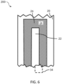
- FIG. 6 is a perspective top view layout of a single unit cell embodiment 200 as shown in FIG. 3 .
- multiple single unit cells may be connected in parallel with the alternating gate regions 20 and the anode regions 22.
- the anode region 22 is surrounded by the source region 24 mesa and the source region mesa 24 is itself surrounded by the gate region 20.
- the electrical coupling 34 is used to electrically connect the anode electrode (not shown) to the source electrode 26 that is disposed over a top surface of the source region 24.
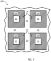
- FIG. 7 is a perspective top view layout of altering depletion-mode trench gate vertical JFETs with an integrated source-drain anti-parallel diodes 600.
- the cell layout comprises the anode region 22 of multiple diode cells that are fully surrounded by source mesas (not shown) having the source electrode 26 over their top surfaces.
- the gate regions 20 form a grid pattern between the isolated anode regions 22 surrounded by source region 24 mesas covered with the source electrodes 26.
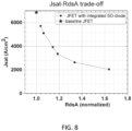
- the curve chart of FIG. 8 shows that compared with the baseline obtained from a conventional trench VJFET design with no integrated source-drain diode, the integration of a source-drain anti-parallel diode reduces J sat values by approximately 50% with minimal impact (approximately 20% increase) on R DS A.
- the substantial reduction of J sat may significantly improve the short-circuit withstand time, allowing for more time for protective circuitry to shut-off the gate of the VJFET in case of a short-circuit event.
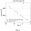
- the curve chart of FIG. 9 further illustrates that compared with the baseline obtained from a conventional trench VJFET design with no integrated source-drain diode, the integration of a source-drain anti-parallel diode into a trench VJFET structure allows for a significant reduction of saturation current density (J sat ) with minimal impact on the threshold voltage (V th ).
- FIG. 10 shows a modeled curve chart of gate-source breakdown voltage (BV GS ) versus the threshold voltage (V th ) for the single unit cell 200 embodiment of a trench VJFET with an integrated anti-parallel source-drain as shown in FIG. 3 .
- V GS gate-source breakdown voltage
- V th threshold voltage
- VJFETs vertical junction field-effect transistors
- MOSFET metal oxide semiconductor field-effect transistor
Landscapes
- Junction Field-Effect Transistors (AREA)
- Metal-Oxide And Bipolar Metal-Oxide Semiconductor Integrated Circuits (AREA)
Abstract
Description
- This application claims the benefit of provisional patent application serial number
63/477,724, filed December 29, 2022 - The present disclosure relates generally to semiconductor technology and in particular to depletion-mode trench gate vertical junction field-effect transistors with integrated source-drain anti-parallel diodes.
- Vertical junction field-effect transistors (VJFETs) built on silicon carbide (SiC) are of great interest for high-power conversion applications and power electronic circuits. Conventional trench VJFET structures are created by etching trenches into a topside of a semiconductor material wherein gate regions are formed on both sides and bottoms of the trenches such that mirror-image replicates of gate regions and gate electrodes are formed on either side of each channel region. Therefore, both electrodes on either side of channel regions of conventional VJFETs are gate electrodes, controlling the current flow between drain and source, and creating a high gate-drain capacitance (CGD) and gate-source capacitance (CGS). Furthermore, in conventional VJFETs a reverse current (also referred to as source-drain current or 3rd quadrant current) conduction path does not exist, and current flow between drain and source approaches zero during their operation in the off-state. Such feature, namely having a bi-directional current flow or providing a 3rd quadrant current-conduction path with a reduced source-drain voltage (VSD) drop, may be utilized in power converter topologies and applications.
- Moreover, while a dual gate cascode structure of a VJFET in series with a low-voltage metal oxide semiconductor field-effect transistor (MOSFET) (herein after referred to as the "cascode structure") reduces the on-state resistance by driving the VJFET into positive VGS values and provides an improved control of switching characteristics by enabling the gate of the VJFET device to be directly driven; nonetheless, cascode structures utilized in hard switching applications experience excessive 3rd quadrant energy losses due to the 3rd quadrant current (ISD) flowing through the VJFET channel region and the source-drain voltage (VSD) exceeding the absolute value of VJFET's threshold voltage (Vth).
- For these and other reasons, there is a general need to reduce the structural gate-drain capacitance (CGD) and gate-source capacitance (CGS) of VJFET structures with a minimal impact to their on-state operation behavior. Furthermore, having a 3rd quadrant current conduction path with a minimal source-drain voltage (VSD) drop and a specific on-resistance in cascode configuration is desired. A reduced specific on-resistance in cascode configuration provides a better control over switching characteristics of the cascode structure, leading to a reduction in energy losses.
- The present disclosure provides improved design structures through incorporation of anti-parallel source-drain diode cells into depletion-mode trench VJFET cells. The integration of an anti-parallel source-drain diode cell into a depletion-mode trench VJFET cell reduces the structural gate-drain capacitance (CGD), gate-source capacitance (CGS), and switching energy losses. Said integration further reduces the saturation current density (Jsat) while maintaining the same threshold voltage (Vth) with minimal impact on the specific on-resistance (RdsA) of trench VJFET cells.
- Depletion-mode trench VJFET cells with integrated source-drain diodes maintain an improved switching performance and reduced switching losses. A reduction in saturation current density provides a longer cascode short-circuit withstand time and an improved safe-operating area (SOA). In the event of a 3rd quadrant current surge, the current is uniformly distributed across the active area of the body region, which reduces the probability of a stacking fault growth. Lastly, having a directly accessible gate electrode forms a dual gate cascode configuration, which allows the VJFET's channel to be turned on during the 3rd quadrant operation.
- Particular embodiments are set out in the independent claims. Various optional examples are set out in the dependent claims. Embodiments of the present disclosure provide vertical junction field-effect transistors (VJFETs) monolithically integrated with anti-parallel PN diodes. These structures can be connected in series with a low-voltage metal oxide semiconductor field-effect transistor (MOSFET) to form a dual gate cascode structure.
- In one aspect, a semiconductor structure comprising a drain-cathode electrode, a substrate over the drain-cathode electrode, and a body region over the substrate is disclosed wherein the body region comprises a top surface, a first source region extending into the body region from the top surface, a first
U-shaped gate region having a portion below the first source region and defining a first gate trench, and a U-shaped anode region having a first portion below the first source region and defining an anode trench. The semiconductor structure further comprises a first source electrode over the first source region and between the first gate trench and the anode trench, a first gate electrode over a portion of a bottom surface of the first gate trench, and an anode electrode over a portion of a bottom of the anode trench, wherein the first source electrode and the anode electrode are electrically coupled, the first gate region forms part of a first vertical junction field-effect transistor (JFET) cell, and the anode region forms part of a vertical diode cell, which is coupled anti-parallel with the first vertical JFET cell. The substrate and the body region may comprise silicon carbide. The first gate region and the anode region may be doped with a p-type dopant and a remaining portion of the body region and the substrate may be doped with an n-type dopant. - In an embodiment, the first source electrode and the anode electrode may integrally form part of a continuous electrode structure that covers at least a portion of the first source region, a portion of a first side wall of the anode trench, and a portion of the bottom of the anode trench. In an alternative embodiment, the first source electrode and the anode electrode integrally form part of a continuous electrode structure that covers at least a portion of the first source region, a first side wall of the anode trench, and the bottom of the anode trench.
- The body region further comprises a first channel region below the first source region and between the first gate region and the anode region. The semiconductor structure may further comprise a secondary channel region doped with an n-type dopant and extending vertically into a central region within the first channel region wherein the maximum doping concentration of the secondary channel region is at least 50% higher than minimum doping concentration of the first channel region. In another embodiment, the semiconductor structure comprises a pair of secondary channel regions doped with n-type dopants and extending on the vertical inner walls within the first channel region wherein the maximum doping concentration of the secondary channel regions is at least 50% higher than minimum doping concentration of the first channel region.
- The semiconductor structure may further comprise a second source region extending into the body region from the top surface, a second U-shaped gate region having a portion below the second source region and defining a second gate trench wherein the anode region has a second portion below the second source region such that the anode trench is between the first gate trench and the second gate trench, a second source electrode over the second source region and between the second gate trench and the anode trench, and a second gate electrode over a portion of a bottom surface of the second gate trench, wherein the first source electrode, the second source electrode, and the anode electrode are electrically coupled, wherein the second gate region forms part of a second vertical JFET cell located on the opposite side of the first vertical JFET cell from the vertical diode cell, and the vertical diode cell is coupled anti-parallel with the first vertical JFET cell and the second vertical JFET cell. The substrate and the body region may comprise silicon carbide. The first gate region, the second gate region, and the anode region may be doped with a p-type dopant and remaining portions of the body region and the substrate are doped with an
n-type dopant. - In an embodiment, the first source electrode, the second source electrode, and the anode electrode integrally form part of a continuous electrode structure that covers at least a portion of the first source region, at least a portion of the second source region, a portion of a first side wall of the anode trench, a portion of the bottom of the anode trench, and a portion of second side wall of the anode trench. Alternatively, the first source electrode, the second source electrode, and the anode electrode integrally form part of a continuous electrode structure that covers at least a portion of the first source region, a portion of the second source region, a first side wall of the anode trench, the bottom of the anode trench, and a second side wall of the anode trench.
- The semiconductor structure further comprises a dielectric material filling portions of the first gate trench and the second gate trench to isolate the first gate electrode from the first source electrode and to isolate the second gate electrode from the second source electrode. The semiconductor structure further comprises a first metal overlay over the first source electrode, the second source electrode, the first gate trench, the anode trench, and the second gate trench.
- The body region may further comprise a drift layer above the substrate and doped with an n-type dopant. The body region may further comprise a current spreading layer above the drift layer and below the first gate region and the second gate region and doped with an n-type dopant.
- In an embodiment, the body region comprises a first channel region below the first source region and between the first gate region and the anode region and a second channel region below the second source region between the second gate region and the anode region. The semiconductor structure may comprise a first secondary channel region doped with an n-type dopant and extending vertically into a central region of the first channel region and a second secondary channel region doped with an n-type dopant and extending vertically into a central region of the second channel region wherein the maximum doping concentration of the secondary channel region is at least 50% higher than minimum doping concentration of the first channel region. Alternatively, the semiconductor structure may comprise a first pair of secondary channel regions doped with an n-type dopant and extending on the vertical inner walls within the first channel region and a second pair of secondary channel regions doped with an n-type dopant and extending on the vertical inner walls within the second channel region wherein the maximum doping concentrations of the first secondary channel regions and the second secondary channel regions are at least 50% higher than minimum doping concentration of the first channel region.
- In a second aspect of the present disclosure, a device structure is disclosed. The device structure comprises a semiconductor structure comprising a drain-cathode electrode, a substrate over the drain-cathode electrode, and a body region over the substrate. The body region comprises a top surface, a first source region extending into the body region from the top surface, a first
U-shaped gate region having a portion below the first source region and defining a first gate trench, and a U-shaped anode region having a first portion below the first source region and defining an anode trench. The semiconductor structure further comprises a first source electrode over the first source region and between the first gate trench and the anode trench, a first gate electrode over a portion of a bottom surface of the first gate trench, an anode electrode over a portion of a bottom of the anode trench, wherein the first source electrode and the anode electrode are electrically coupled, the first gate region forms part of a first vertical junction field-effect transistor (JFET) cell, and the anode region forms part of a vertical diode cell, which is coupled anti-parallel with the first vertical JFET cell. The device structure further comprises a metal oxide semiconductor field-effect transistor (MOSFET) comprising a gate electrode, a source electrode, and a drain electrode, wherein the drain electrode of the MOSFET is coupled in series to the first source electrode of the first vertical JFET cell coupled anti-parallel with the vertical diode cell, forming a dual-gate cascode FET device. - In an embodiment, the semiconductor structure further comprises a second source region extending into the body region from the top surface, a second U-shaped gate region having a portion below the second source region and defining a second gate trench, wherein the anode region has a second portion below the second source region such that the anode trench is between the first gate trench and the second gate trench, a second source electrode over the second source region and between the second gate trench and the anode trench, a second gate electrode over a portion of a bottom surface of the second gate trench, wherein the first source electrode, the second source electrode, and the anode electrode are electrically coupled, and wherein the second gate region forms part of a second vertical JFET cell located on the opposite side of the first vertical JFET cell from the vertical diode cell, and the vertical diode cell is coupled anti-parallel with the first vertical JFET cell and the second vertical JFET cell.
- In a third aspect of the present disclosure a method of fabricating a semiconductor structure is disclosed. The method comprises providing a drain-cathode electrode, providing a substrate over the drain-cathode electrode, providing a body region over the substrate wherein the body region comprises a top surface, a first source region extending into the body region from the top surface, a first U-shaped gate region having a portion below the first source region and defining a first gate trench, and a U-shaped anode region having a first portion below the first source region and defining an anode trench. The method further comprises providing a first source electrode over the first source region and between the first gate trench and the anode trench, providing a first gate electrode over a portion of a bottom surface of the first gate trench, providing an anode electrode over a portion of a bottom of the anode trench, and electrically coupling the first source electrode and the anode electrode such that the first gate region forms part of a first vertical junction field-effect transistor (JFET) cell, and the anode region forms part of a vertical diode cell, which is coupled anti-parallel with the first vertical JFET cell.
- In another aspect, any of the foregoing aspects individually or together, and/or various separate aspects and features as described herein, may be combined for additional advantage. Any of the various features and elements as disclosed herein may be combined with one or more other disclosed features and elements unless indicated to the contrary herein.
- Those skilled in the art will appreciate the scope of the present disclosure and realize additional aspects thereof after reading the following detailed description of the preferred embodiments in association with the accompanying drawing figures.
- The accompanying drawing figures incorporated in and forming a part of this specification illustrate several aspects of the disclosure, and together with the description serve to explain the principles of the disclosure.
-
FIGS. 1A and1B illustrate cross-sectional views of embodiments of depletion-mode trench gate vertical junction field-effect transistors (VJFETs) with integrated source-drain anti-parallel diodes. -
FIG. 2 shows an dual-gate cascode FET configuration comprising a plurality of alternating trench VJFET cells and anti-parallel source-drain diode cells connected in series with a metal oxide semiconductor field-effect transistor (MOSFET). -
FIG. 3 illustrates a perspective view of a trench VJFET with an integrated anti-parallel source-drain diode forming a single unit cell having a gate-drain capacitance CGD and a gate-source capacitance CGS. -
FIG. 4 depicts the electron flow lines through a single unit cell embodiment as illustrated schematically with flow lines. -
FIGS. 5A-5C depict embodiments of single unit cells having one or more secondary vertical channel regions. -
FIG. 6 is a perspective top view layout of a single unit cell embodiment as shown inFIG. 3 . -
FIG. 7 is a perspective top view layout of altering depletion-mode trench gate VJFETs with integrated source-drain anti-parallel diodes. -
FIG. 8 shows a modeled curve chart of saturation current density (Jsat) versus the specific on-resistance (RDSA) for a single unit cell embodiment as shown inFIG. 3 . -
FIG. 9 shows a modeled curve chart of saturation current density (Jsat) versus the threshold voltage (Vth) for a single unit cell embodiment as shown inFIG. 3 . -
FIG. 10 shows a modeled curve chart of gate-source breakdown voltage (BVGS) versus the threshold voltage (Vth) for a single unit cell embodiment as shown inFIG. 3 . - The embodiments set forth below represent the necessary information to enable those skilled in the art to practice the embodiments and illustrate the best mode of practicing the embodiments. Upon reading the following description in light of the accompanying drawing figures, those skilled in the art will understand the concepts of the disclosure and will recognize applications of these concepts not particularly addressed herein. It should be understood that these concepts and applications fall within the scope of the disclosure and the accompanying claims.
- It should be understood that, although the terms first, second, etc. may be used herein to describe various elements, these elements should not be limited by these terms. These terms are only used to distinguish one element from another. For example, a first element could be termed a second element, and, similarly, a second element could be termed a first element, without departing from the scope of the present disclosure. As used herein, the term "and/or" includes any and all combinations of one or more of the associated listed items.
- It should also be understood that when an element is referred to as being "connected" or "coupled" to another element, it can be directly connected or coupled to the other element or intervening elements may be present. In contrast, when an element is referred to as being "directly connected" or "directly coupled" to another element, there are no intervening elements present.
- It should be understood that, although the terms "upper," "lower," "bottom," "intermediate," "middle," "top," and the like may be used herein to describe various elements, these elements should not be limited by these terms. These terms are only used to distinguish one element from another. For example, a first element could be termed an "upper" element and, similarly, a second element could be termed an "upper" element depending on the relative orientations of these elements, without departing from the scope of the present disclosure.
- The terminology used herein is for the purpose of describing particular embodiments only and is not intended to be limiting of the disclosure. As used herein, the singular forms "a," "an," and "the" are intended to include the plural forms as well, unless the context clearly indicates otherwise. It will be further understood that the terms "comprises," "comprising," "includes," and/or "including" when used herein specify the presence of stated features, integers, steps, operations, elements, and/or components, but do not preclude the presence or addition of one or more other features, integers, steps, operations, elements, components, and/or groups thereof.
- Unless otherwise defined, all terms (including technical and scientific terms) used herein have the same meaning as commonly understood by one of ordinary skill in the art to which this disclosure belongs. It will be further understood that terms used herein should be interpreted as having meanings that are consistent with their meanings in the context of this specification and the relevant art and will not be interpreted in an idealized or overly formal sense unless expressly so defined herein.
- Embodiments are described herein with reference to schematic illustrations of embodiments of the disclosure. As such, the actual dimensions of the layers and elements can be different, and variations from the shapes of the illustrations as a result, for example, of manufacturing techniques and/or tolerances, are expected. For example, a region illustrated or described as square or rectangular can have rounded or curved features, and regions shown as straight lines may have some irregularity. Thus, the regions illustrated in the figures are schematic and their shapes are not intended to illustrate the precise shape of a region of a device and are not intended to limit the scope of the disclosure. Additionally, sizes of structures or regions may be exaggerated relative to other structures or regions for illustrative purposes and, thus, are provided to illustrate the general structures of the present subject matter and may or may not be drawn to scale. Common elements between figures may be shown herein with common element numbers and may not be subsequently
- Conventional trench vertical junction field-effect transistor (VJFET) structures are created by etching trenches into a topside of a semiconductor material wherein gate regions are formed on both sides and bottoms of the trenches such that mirror-image replicates of gate regions and gate electrodes are formed on either side of each channel region. Therefore, both electrodes on either side of channel regions of conventional VJFETs are gate electrodes, controlling the current flow between drain and source, and creating a high gate-drain capacitance (CGD) and gate-source capacitance (CGS). Furthermore, in conventional VJFETs a reverse current (also referred to as source-drain current or 3rd quadrant current) conduction path does not exist, and current flow between drain and source approaches zero during their operation in the off-state. Such feature, namely having a bi-directional current flow or providing a 3rd quadrant current-conduction path with a reduced source-drain voltage (VSD) drop, may be utilized in power converter topologies and applications.
- Moreover, while a dual gate cascode structure of a VJFET in series with a low-voltage metal oxide semiconductor field-effect transistor (MOSFET) (herein after referred to as the "cascode structure") reduces the on-state resistance by driving the VJFET into positive VGS values and provides an improved control of switching characteristics by enabling the gate of the VJFET device to be directly driven, nonetheless, cascode structures utilized in hard switching applications experience excessive 3rd quadrant energy losses due to the 3rd quadrant current (ISD) flowing through the VJFET channel region and the source-drain voltage (VSD) exceeding the absolute value of VJFET's threshold voltage (Vth).
- Embodiments of the present disclosure provide VJFETs monolithically integrated with anti-parallel PN diodes. These structures can be applied to a variety of semiconductor devices including but not limited to other types of transistors and diodes and to other e-channel and p-channel JFET structures. A normally-off operation mode can be implemented by connecting the normally-on VJFET with an anti-parallel diode structure to a low-voltage MOSFET in a cascode configuration.
- Merely by way of example, the concepts described herein have been applied to integration of these structures in silicon carbide (SiC) or gallium nitride (GaN). Other wide bandgap materials may be used for the integration of various embodiments disclosed herein. Alternatively, silicon (Si) (another primary semiconductor used in power electronic devices) may be used for the integration of various embodiments disclosed herein. SiC material properties make SiC JFETs attractive for high power conversion and high-power density applications. SiC JFETs are also of great interest in power electronic circuits for high-frequency power applications or circuit protection functions due to their superior performance compared with similar devices built on silicon.
- It is to be appreciated that certain features of the disclosure which are, for clarity, described herein in the context of separate embodiments may also be provided in combination in a single embodiment. Conversely, various features of the present disclosure that are, for brevity, described in the context of a single embodiment may also be provided separately or in any sub-combination.
-
FIGS. 1A and1B illustrate cross-sectional views of embodiments of depletion-mode trench gate VJFETs with integrated source-drain anti-parallel diodes. It should be understood that the structures illustrated inFIGS. 1A and1B are and are simplified and that the scope of the present disclosure is not limited to these specific examples. Furthermore, the dimensions in the figures of this application are not to scale, and at times the relative dimensions are exaggerated or reduced in size to more clearly show various structural features. - While only three trenches are shown in each figure, it is to be understood that the structures illustrated may be replicated many times in an actual semiconductor device. Also, while due to the higher mobility of electrons compared with that of holes in SiC, the majority carriers in structures illustrated in these figures are electrons. It is further to be understood that the structures illustrated may be replicated with holes as the majority carriers in the case of which polarity signs and the directions of electric field and electric flux density may be reversed.
-
FIG. 1A illustrates a cross-sectional view of an embodiment of depletion-mode trench gate vertical JFETs (VJFETs) with integrated source-drain anti-parallel diodes (herein after referred to as "VJFET-diode structure 100") which are built on a wafer comprising asubstrate 10 and abody region 12, both of which are doped with an n-type dopant. - A
source region 24 extends into a top surface of thebody region 12 using an ion implantation or epitaxial growth process. Ananode trench 14, afirst gate trench 16a, and asecond gate trench 16b are formed by etching trenches into a top surface of thebody region 12 such that each trench extends vertically downward into thebody region 12 from the top surface thereof. Although
FIG. 1A illustrates examples of trenches according to some embodiments of the present disclosure, it will be understood that the present disclosure is not limited to such configurations. For example, trenches adjacent to each other as described in the first embodiment may be of different depths or different widths. In various embodiments, adjacent trenches may dispose a different distance apart from one another. - The
anode trench 14, thefirst gate trench 16a, and thesecond gate trench 16b form afirst source region 24a and asecond source region 24b as part of thesource region 24. Thefirst source region 24a is formed under the top surface of thebody region 12 between thefirst gate trench 16a and theanode trench 14, and thesecond source region 24b is formed under the top surface of thebody region 12 between thesecond gate trench 16b and theanode trench 14. Thesource region 24, which includes thefirst source region 24a and thesecond source region 24b, is doped with an n+ dopant having a doping concentration ranging from 5e17 cm-3 to 1e21 cm-3. It should be appreciated that the thickness and doping concentration of thesource region 24 may vary according to applications and fabrication processes. - Under the
source region 24, bottom and sidewalls surrounding each of thefirst gate trench 16a, thesecond gate trench 16b, and theanode trench 14 are doped with a p-type dopant to form afirst gate region 20a, asecond gate region 20b, and ananode region 22, respectively, such that thefirst gate region 20a forms a U-shaped region under thesource region 24 that defines thefirst gate trench 16a with a first portion of the U-shaped region under thefirst source region 24a. Similarly, theanode region 22 forms a U-shaped region under thesource region 24 to define theanode trench 14 with a first portion of the U-shaped region under thefirst source region 24a. - The doping process is through ion implantation using vertical and/or angled implants and may combine multiple implantation energies and tilt and rotation angles and may be performed at high temperature (above room temperature) while the doping type of the dopant used is opposite that of the
body region 12. In one embodiment, trench sidewalls may be partially implanted or have a narrower doped region to reduce the structure's specific on-resistance (RdsA). The doping type of thefirst gate region 20a, thesecond gate region 20b, and theanode region 22 are opposite those of thesource region 24, thebody region 12, and thesubstrate 10. Thefirst gate region 20a, thesecond gate region 20b, and theanode region 22 may have a doping concentration ranging from 1e17cm-3 to 5e20cm-3. - In practice, ohmic contacts may be used to reduce the contact resistance between the semiconductor and the metal electrodes and to enhance the overall conductance of the VJFET-
diode structure 100. Therefore, a first and a second source ohmic contacts (not shown here for simplicity and clarity) may form part of thefirst source region 24a between thefirst gate trench 16a and theanode trench 14 and of thesecond source region 24b between thesecond gate trench 16b and theanode trench 14. The heavily dopedn+ source region 24 forms PN junctions with thefirst gate region 20a, thesecond gate region 20b, and theanode region 22, which facilitates gate control in the JFET cell. Similarly, a drain ohmic contact (not shown) may form part of a back surface of thesubstrate 10, a first and a second gate ohmic contact (not shown) may form part of bottom surfaces of thefirst gate trench 16a and thesecond gate trench 16b, and an anode ohmic contact (not shown) may form part of a bottom surface of theanode trench 14. - A
first channel region 18a and asecond channel region 18b form part of thebody region 12. Thefirst channel region 18a extends vertically into thebody region 12 from below thefirst source region 24a and forms laterally in between thefirst gate region 20a and theanode region 22. Thesecond channel region 18b extends vertically into thebody region 12 below thesecond source region 24b and forms laterally in between theanode region 22 and thesecond gate region 20b. It should be noted that while only two channel regions are shown inFIG. 1A , the structures illustrated may be replicated many times to form a plurality of channel regions in a semiconductor device designed according to disclosures of the present application. - As shown in
FIG. 1A , metal deposits over top surfaces ofsource regions 24form source electrodes 26 including afirst source electrode 26a covering the top surface of thefirst source region 24a and between thefirst gate trench 16a and theanode trench 14 and asecond source electrode 26b covering the top surface of thesecond source region 24b and between thesecond gate trench 16b and theanode trench 14. Similarly, metal regions over at least a portion of bottom surfaces of thefirst gate trench 16a and asecond gate trench 16b provide afirst gate electrode 30a and asecond gate electrode 30b. Metal deposits over at least a portion of a bottom surface of theanode trench 14 provide ananode electrode 28, and metal deposits over a backside surface of thesubstrate 10 provide a drain-cathode electrode 32.Electrical couplings 34 are used to electrically connect each of thefirst source electrode 26a and thesecond source electrode 26b to theanode electrode 28 in order to hold theanode electrode 28 at the same electrical potential as thefirst source electrodes 26a and thesecond source electrode 26b. - In the simplified cross-sectional view of the embodiment shown in
FIG. 1A , theanode electrode 28, theanode region 22, and the drain-cathode electrode 32 form part of avertical diode cell 40. As part of the same VJFET-diode structure 100, thefirst source electrode 26a and thefirst source region 24a along with the drain-cathode electrode 32, thefirst gate electrode 30a, and thefirst gate region 20a form part of afirst VJFET cell 36. Similarly, thesecond source electrode 26b and thesecond source region 24b along with the drain-cathode electrode 32, thesecond gate electrode 30b, and thesecond gate region 20b form part of asecond VJFET cell 38, which is located on the opposite side of thefirst VJFET cell 36 from thevertical diode cell 40, and thevertical diode cell 40 is coupled anti-parallel with thefirst VJFET cell 36 and thesecond VJFET cell 38. - A
single unit cell 200 as shown in the embodiment ofFIG. 1A includes portions of thefirst VJFET cell 36 and portions of thevertical diode cell 40 adjacent to it. The integration of the source-drain anti-parallel diode into the depletion-mode trench VJFET semiconductor structure allows a 3rd quadrant current conduction while the VJFET is in off-state with a significant reduction of saturation current density (Jsat) and maintaining a similar threshold voltage (Vth) and specific on-resistance (RdsA). -
FIG. 1B shows a cross-sectional view of an embodiment of depletion-mode trench gate VJFET with integrated source-drain anti-parallel diodes (herein after referred to as "VJFET-diode structure 100"). As shown inFIG. 1B , thebody region 12 may further comprise an n-type drift layer 42 configured to withstand a desired blocking voltage. Thedrift layer 42 may form above thesubstrate 10 and have a doping level in the range of 2e14cm-3 to 5e16cm-3. The doping level of thebody region 12 may be in the ranges of 2e14cm-3 to 1e17cm-3, and the doping level of thesubstrate 10 may be in the range of 2e17cm-3 to 1e19cm-3. - The
body region 12 compriseschannel regions 18 including thefirst channel region 18a and thesecond channel region 18b. Thefirst channel region 18a forms below thefirst source region 24a and between thefirst gate region 20a and theanode region 22. Thesecond channel region 18b forms below thesecond source region 24b and between thesecond gate region 20b and theanode region 22. The doping level of thechannel regions 18, including thefirst channel region 18a and thesecond channel region 18b, may be at least two times lower than the lowest doping concentration in the rest of thebody region 12 and in the range of 1e14cm-3 to 2e16cm-3. - The
body region 12 may also comprise an n-type current spreadinglayer 44, which may have a doping level in the range of 1e16cm-3 to 1e17cm-3. The current spreadinglayer 44 may be continuous or segmented and form above thedrift layer 42 with its upper boundary positioned below thefirst gate region 20a and thesecond gate region 20b. The current spreadinglayer 44 may further comprise a plurality of other layers of different doping levels formed epitaxially and/or by ion implantation. - Optionally, a heavily doped N-type buffer layer (not shown here) may form over a top surface of the
substrate 10 by means of epitaxial growth. It is further noted that while thebody region 12, thesubstrate 10, thefirst channel region 18a, and thesecond channel region 18b, buffer, the current spreadinglayer 44, andsource regions 24 including thefirst source region 24a and thesecond source region 24b are depicted to have had been doped with an n-type dopant, and while agate region 20 and theanode region 22 are shown with a p-type dopant, in practice, the doping types can be switched among these same structures. - In an embodiment, the
first source electrode 26a and theanode electrode 28 integrally form part of a continuous electrode structure 26' that covers over at least a portion of thefirst source region 24a to provide thefirst source electrode 26a, a portion of a first side wall of theanode region 22 adjacent to thefirst source electrode 26a to form afirst sidewall electrode 26d, and a portion of the bottom ofanode trench 14 to form a bottom surface (anode)electrode 26c. According to another embodiment, thefirst source electrode 26a and theanode electrode 28 integrally form part of the continuous electrode structure 26' that covers over at least a portion of thefirst source region 24a to provide thefirst source electrode 26a, the first side wall of theanode region 22 adjacent to thefirst source electrode 26a to form thefirst sidewall electrode 26d, and the bottom ofanode trench 14 to form the bottom surface (anode)electrode 26c. - The
first source electrode 26a, thesecond source electrode 26b, and theanode electrode 28 may integrally form part of a continuous electrode structure 26' that covers at least a portion of thefirst source region 24a to provide thefirst source electrode 26a, a portion of the first side wall of theanode region 22 adjacent to thefirst source electrode 26a to form thefirst sidewall electrode 26d, a portion of the bottom ofanode trench 14 to form the bottom surface (anode)electrode 26c, a portion of the second side wall of theanode region 22 adjacent to thesecond source electrode 26b to form thesecond sidewall electrode 26e, and at least a portion of thesecond source region 24b to provide thesecond source electrode 26b. - In yet another embodiment, the
first source electrode 26a, thesecond source electrode 26b, and theanode electrode 28 integrally form part of a continuous electrode structure 26' that covers at least a portion of thefirst source region 24a to provide thefirst source electrode 26a, the first side wall of theanode region 22 adjacent to thefirst source electrode 26a to form thefirst sidewall electrode 26d, the bottom ofanode trench 14 to form the bottom surface (anode)electrode 26c, the second side wall of theanode region 22 adjacent to thesecond source electrode 26b to form asecond sidewall electrode 26e, and at least a portion of thesecond source region 24b to provide thesecond source electrode 26b. - A mostly self-aligned silicidation (salicidation) process may be used to form a separated first and
second gate electrodes first source electrode 26a of thefirst VJFET cell 36 with the bottom surface (anode)electrode 26c of thevertical diode cell 40 and thesecond source electrode 26b of thesecond VJFET cell 38. The source metal for silicidation process may include, but not limited to, nickel and titanium. A drain-cathode electrode 32 may be formed by a combination of metal deposition and laser irradiation. - The structure of
FIG. 1B depicts an embodiment wherein thefirst gate trench 16a and thesecond gate trench 16b are filled with a gatetrench dielectric material 48. The gatetrench dielectric material 48 is used to ensure the electrical isolation of thefirst source electrode 26a and thefirst gate electrode 30a in thefirst VJFET cell 36 and the electrical isolation of thesecond source electrode 26b andsecond gate electrode 30b in thesecond VJFET cell 38. - In an embodiment, the
anode trench 14 is filled with an anodetrench dielectric material 46. A portion of the anodetrench dielectric material 46 may be removed in order to maximize the exposure of the continuous electrode structure 26'. The method and process of fabrication used may control the amount of anodetrench dielectric material 46 that is removed from theanode trench 14. In another embodiment, the anodetrench dielectric material 46 is entirely removed from theanode trench 14, allowing the trench to be fully filled with afirst metal overlay 50. Thefirst metal overlay 50 is deposited over the topside of the semiconductor structure to form a thick metal overlay which improves the conductivity of source-anode electrical connection. - The
first metal overlay 50 coverssource electrodes 26 and the exposed portions of the continuous electrode structure 26' while filling theanode trench 14 to replace the removed portions of the anodetrench dielectric material 46 to form contact with portions of thefirst sidewall electrode 26d and thesecond sidewall electrode 26e. Thefirst metal overlay 50 may combine different metal sub-layers (not shown) including but not limited to metal layers composed of aluminum (Al), aluminum-copper (Al-Cu), copper (Cu), titanium (Ti), tungsten-titanium (TiW), tungsten (W), titanium nitride (TiN), palladium (Pd), and gold (Au). - In an embodiment, a final topside passivation layer (not shown) comprising a combination of chemical vapor deposition (CVD) dielectrics and polyimide may be deposited over the top surface of the
first metal overlay 50 at a periphery of a semiconductor die used to fabricate VJFET-diode structure 100. - A
second metal overlay 52 is deposited at least partially over the backside of the drain-cathode electrode 32. Multiple metallization layers (not shown) including one or more of Ni, Ti, TiW, TiN, W, Pd, Au, and silver (Ag) may comprise thesecond metal overlay 52. - Basal plane defect (BPD) and stacking fault screening has to be implemented on starting an epitaxial wafer and at device level in the same manner as it is implemented in silicon carbide MOSFETs with built-in source-drain diode.
-
FIG. 2 shows an dual-gatecascode FET configuration 300 comprising a plurality of alternating trench VJFET cells and anti-parallel source-drain diode cells (herein after referred to as "VJFET/diode structure 100‴) connected in series with aMOSFET 70. The VJFET/diode structure 100' comprises a unified drain electrode 52', a unified gate electrode 30', and a unified source electrode 50'. TheMOSFET 70 may be a low-voltage transistor having aMOSFET drain electrode 72, aMOSFET gate electrode 74, and aMOSFET source electrode 76. TheMOSFET drain electrode 72 is coupled to the unified source electrode 50' of the VJFET/diode structure 100' forming anintermediary electrode 80 for the dual-gatecascode FET configuration 300 having adrain electrode 82, asource electrode 84, afirst gate electrode 86, and asecond gate electrode 88. Thefirst gate electrode 86 is the unified gate electrode 30' of the VJFET/diode structure 100', and thesecond gate electrode 88 is theMOSFET gate electrode 74. Thedrain electrode 82 is the unified drain electrode 52' of the VJFET/diode structure 100', and thesource electrode 84 is theMOSFET source electrode 76. The dual-gatecascode FET configuration 300 reduces the on-resistance of VJFET/diode structure 100'. The unified gate electrode 30' of the VJFET/diode structure 100' can be driven into positive VGS values utilizing thefirst gate electrode 86, which further improves controlling of switching behavior of the VJFET/diode structure 100'. Thesecond gate electrode 88, which is theMOSFET gate electrode 74, provides general on/off control for the dual-gatecascode FET configuration 300. -
FIG. 3 illustrates a perspective view of a trench VJFET with an integrated anti-parallel source-drain diode forming asingle unit cell 200 having a gate-drain capacitance C GD 58 and a gate-source capacitance C GS 60. Thesingle unit cell 200 comprises a VJFET side of thecell 54 and an anti-parallel diode side of thecell 56. The VJFET side of thecell 54 comprises agate region 20, asource region 24, asource electrode 26, agate electrode 30, and a drain-cathode electrode 32. The anti-parallel diode side of thecell 56 comprises ananode region 22, ananode electrode 28, and the drain-cathode electrode 32. Thesource electrode 26 and theanode electrode 28 are electrically connected using anelectrical coupling 34. Achannel region 18 forms under thesource region 24 and extends vertically into thebody region 12 and laterally in between thegate region 20 and theanode region 22. - The integration of an anti-parallel source-drain diode within a trench VJFET structure to form the
single unit cell 200 reduces the gate-drain capacitance C GD 58 by approximately 50% to a first gate-drain capacitance C GD 58a and by eliminating a second gate-drain capacitance C GD 58b. Similarly, the integration of an anti-parallel source-drain diode within a trench VJFET structure to form thesingle unit cell 200 reduces the gate-source capacitance C GS 60 by approximately 50% to a first gate-source capacitance C GS 60a and by eliminating a second gate-source capacitance C GS 60b. - Replacing a second gate electrode of the conventional VJFET (not shown) with the
anode electrode 28 and electrically connecting thesource electrode 26 to theanode electrode 28 forms an anti-parallel source-drain PN diode that eliminates associated parasitic capacitances with minimal impact on the on-resistance of thesingle unit cell 200. Cancelled portions of the parasitic gate-drain capacitance C GD 58 and the gate-source capacitance C GS 60 improve the switching behavior of thesingle unit cell 200 with minimal impact on the on-state behavior of the device. Persons skilled in the art will appreciate that the aforementioned positive effect becomes more pronounced when multiplesingle unit cells 200 of a vertical trench JFET with integrated source-drain anti-parallel diodes are connected alternating and in parallel as shown inFIGS. 1A and1B . -
FIG. 4 depicts the electron flow lines (forward current flow is in the opposite direction) through asingle unit cell 200 embodiment as illustrated schematically with electron flow lines. As shown inFIG. 4 , in the 1st quadrant of the conduction mode, forward current flow occurs through both the VJFET side of thecell 54 and the anti-parallel diode side of thecell 56. The forward current through the VJFET side of thecell 54 as illustrated schematically with VJFETcurrent flow lines 62 and the forward current through the diode side of thecell 56 as illustrated schematically with diodecurrent flow lines 64 illustrate the minimal impact of integrating a source-drain anti-parallel diode within the device structure as forward current continues to spread efficiently through the entire structure. -
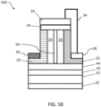
FIGS. 5A-5C depict embodiments of a firstsingle unit cell 400, a secondsingle unit cell 500, and a thirdsingle unit cell 550, respectively, each having one or more secondaryvertical channel regions 66. The one or more secondaryvertical channel regions 66 as shown inFIGS. 5A and5C may be formed either by angled ion implantation or by vertical ion implantation or a combination of both. - The doping levels of the
channel region 18, which may further comprise one or more secondaryvertical channel regions 66, affects the operation of the anti-parallel source-drain diode within a trench VJFET to form thesingle unit cell 200. The threshold voltage (Vth) can be optimized through adjusting the doping level of thechannel region 18 to a value that is much lower than that of the rest of thebody region 12 and thesubstrate 10. For example, the doping level of thechannel region 18 may be at least two times lower than the lowest doping concentration in the rest of thebody region 12 and in the range of 1e14cm-3 to 2e16cm-3. Furthermore, the maximum doping concentration of the one or more secondaryvertical channel regions 66 as shown inFIGS. 5A and5B may be at least 50% higher than the minimum concentration in thechannel region 18. - As illustrated in
FIG. 5A , thechannel region 18 may further comprise one or more secondaryvertical channel regions 66, wherein the one or more secondaryvertical channel regions 66 run alongside the sidewalls of thechannel region 18. In one embodiment, the one or more secondaryvertical channel regions 66 may have a maximum doping level that is at least 50% higher than minimum doping level in thechannel region 18. -
FIG. 5B illustrates an embodiment of a secondaryvertical channel region 66, wherein the secondaryvertical channel region 66 runs alongside the center of thechannel region 18. The secondaryvertical channel region 66 as shown inFIG. 5B has a maximum doping level that is at least 50% higher than a minimum doping level of thechannel region 18. -
FIG. 5C illustrates an embodiment of a secondaryvertical region 66, wherein the secondaryvertical channel region 66 runs along the sidewall of thechannel region 18 that is one the side of thegate electrode 30 but there is no secondaryvertical region 66 on the sidewall on the side of theanode 28. By placing the secondaryvertical region 66 only on the sidewall adjacent to thegate electrode 30, the process of manufacturing the thirdsingle unit cell 550 is simplified since secondaryvertical channel region 66 only has to be implemented on one sidewall. Furthermore, in some embodiments, the benefit of having another secondaryvertical channel region 66 along the side of the body like the firstsingle unit cell 400 may be limited since thegate electrode 30 will primarily affect the operation of the adjacent secondary vertical channel in both forward conduction and off-state blocking.. -
FIG. 6 is a perspective top view layout of a singleunit cell embodiment 200 as shown inFIG. 3 . In order to increase the current rating of the device, multiple single unit cells may be connected in parallel with the alternatinggate regions 20 and theanode regions 22. As shown in the top view layout of thesingle unit cell 200 embodiment, theanode region 22 is surrounded by thesource region 24 mesa and thesource region mesa 24 is itself surrounded by thegate region 20. Theelectrical coupling 34 is used to electrically connect the anode electrode (not shown) to thesource electrode 26 that is disposed over a top surface of thesource region 24. -
FIG. 7 is a perspective top view layout of altering depletion-mode trench gate vertical JFETs with an integrated source-drainanti-parallel diodes 600. In an embodiment, the cell layout comprises theanode region 22 of multiple diode cells that are fully surrounded by source mesas (not shown) having thesource electrode 26 over their top surfaces. Thegate regions 20 form a grid pattern between theisolated anode regions 22 surrounded bysource region 24 mesas covered with thesource electrodes 26. -
FIG. 8 shows a modeled curve chart of saturation current density (Jsat) versus the specific on-resistance (RDSA) for thesingle unit cell 200 embodiment of a trench VJFET with an integrated anti-parallel source-drain as shown in
FIG. 3 under operation values of VGS = 0 V and VDS = 800 V. The curve chart ofFIG. 8 shows that compared with the baseline obtained from a conventional trench VJFET design with no integrated source-drain diode, the integration of a source-drain anti-parallel diode reduces Jsat values by approximately 50% with minimal impact (approximately 20% increase) on RDSA. The substantial reduction of Jsat may significantly improve the short-circuit withstand time, allowing for more time for protective circuitry to shut-off the gate of the VJFET in case of a short-circuit event. -
FIG. 9 shows a modeled curve chart of saturation current density (Jsat) versus the threshold voltage (Vth) for thesingle unit cell 200 embodiment of a trench VJFET with an integrated anti-parallel source-drain as shown inFIG. 3 under operation values of VGS = 0 V and VDS = 800 V. The curve chart ofFIG. 9 further illustrates that compared with the baseline obtained from a conventional trench VJFET design with no integrated source-drain diode, the integration of a source-drain anti-parallel diode into a trench VJFET structure allows for a significant reduction of saturation current density (Jsat) with minimal impact on the threshold voltage (Vth). -
FIG. 10 shows a modeled curve chart of gate-source breakdown voltage (BVGS) versus the threshold voltage (Vth) for thesingle unit cell 200 embodiment of a trench VJFET with an integrated anti-parallel source-drain as shown inFIG. 3 . To turn off a normally-on VJFET device, a VGS that is lower (more negative in value) than VJFET's threshold voltage (Vth) must be applied. However, such low value of VGS may deplete thechannel region 18 and result in a punch-through breakdown between thegate region 20 and theanode region 22. As shown in the modeled curve chart, embodiments of the present disclosure provide improved design structures with significant safety margin values (in the range of 20V to 25V) between Vth and their corresponding BVGS, resulting in a feasible structure for practical gate drive conditions. - A computer readable medium may include transitory or non-transitory type media such as physical storage media including storage discs and solid state devices. A computer readable medium may also or alternatively include transient media such as carrier signals and transmission media. A computer-readable storage medium is defined herein as a non-transitory memory device. A memory device includes memory space within a single physical storage device or memory space spread across multiple physical storage devices.
- It is contemplated that any of the foregoing aspects, and/or various separate aspects and features as described herein, may be combined for additional advantage. Any of the various embodiments as disclosed herein may be combined with one or more other disclosed embodiments unless indicated to the contrary herein.
- Those skilled in the art will recognize improvements and modifications to the preferred embodiments of the present disclosure. All such improvements and modifications are considered within the scope of the concepts disclosed herein and the claims that follow.
- Thus, from one perspective, there have now been described vertical junction field-effect transistors (VJFETs) with integrated source-drain anti-parallel diodes. In an embodiment, a trench VJFET with integrated source-drain anti-parallel diodes structure is coupled with a low-voltage metal oxide semiconductor field-effect transistor (MOSFET) in a dual gate cascode configuration.
- Further examples of feature combinations taught by the present disclosure are set out in the following numbered clauses:
- 1. A semiconductor structure comprising:
- a drain-cathode electrode;
- a substrate over the drain-cathode electrode;
- a body region over the substrate comprising:
- a top surface;
- a first source region extending into the body region from the top surface;
- a first U-shaped gate region having a portion below the first source region and defining a first gate trench; and
- a U-shaped anode region having a first portion below the first source region
- and defining an anode trench;
- a first source electrode over the first source region and between the first gate trench and the anode trench;
- a first gate electrode over a portion of a bottom surface of the first gate trench;
- an anode electrode over a portion of a bottom of the anode trench; and
- wherein the first source electrode and the anode electrode are electrically coupled,
- the first gate region forms part of a first vertical junction field-effect transistor (JFET) cell, and the anode region forms part of a vertical diode cell, which is coupled anti-parallel with the first vertical JFET cell.
- 2. The semiconductor structure of clause 1 wherein the substrate and the body region comprise silicon carbide.
- 3. The semiconductor structure of clause 1 or 2 wherein the first gate region and the anode region are doped with a p-type dopant and a remaining portion of the body region and the substrate are doped with an n-type dopant.
- 4. The semiconductor structure of any preceding clause wherein the first source electrode and the anode electrode integrally form part of a continuous electrode structure that covers at least a portion of the first source region, a portion of a first side wall of the anode trench, and a portion of the bottom of the anode trench.
- 5. The semiconductor structure of any preceding clause wherein the first source electrode and the anode electrode integrally form part of a continuous electrode structure that covers at least a portion of the first source region, a first side wall of the anode trench, and the bottom of the anode trench.
- 6. The semiconductor structure of any preceding clause wherein the body region further comprises a first channel region below the first source region and between the first gate region and the anode region.
- 7. The semiconductor structure of clause 6 further comprising a secondary channel region doped with an n-type dopant and extending vertically into a central region within the first channel region.
- 8. The semiconductor structure of clause 7 wherein a maximum doping concentration of the secondary channel region is at least 50% higher than a minimum doping concentration of the first channel region.
- 9. The semiconductor structure of clause 6 further comprising a pair of secondary channel regions doped with n-type dopants and extending on vertical inner walls within the first channel region.
- 10. The semiconductor structure of clause 9 wherein a maximum doping concentration of the secondary channel regions is at least 50% higher than a minimum doping concentration of the first channel region.
- 11. The semiconductor structure of any preceding clause further comprising:
- a second source region extending into the body region from the top surface of the body region;
- a second U-shaped gate region having a portion below the second source region and defining a second gate trench, wherein the anode region has a second portion below the second source region such that the anode trench is between the first gate trench and the second gate trench;
- a second source electrode over the second source region and between the second gate trench and the anode trench; and
- a second gate electrode over a portion of a bottom surface of the second gate trench, wherein the first source electrode, the second source electrode, and the anode electrode are electrically coupled; and
- 12. The semiconductor structure of clause 11 wherein the substrate and the body region comprise silicon carbide.
- 13. The semiconductor structure of
clause 11 or 12 wherein the first gate region, the second gate region, and the anode region are doped with a p-type dopant and remaining portions of the body region and the substrate are doped with an n-type dopant. - 14. The semiconductor structure of any of clauses 11-13 wherein the first source electrode, the second source electrode, and the anode electrode integrally form part of a continuous electrode structure that covers at least a portion of the first source region, at least a portion of the second source region, a portion of a first side wall of the anode trench, a portion of the bottom of the anode trench, and a portion of a second side wall of the anode trench.
- 15. The semiconductor structure of any of clauses 11-14 wherein the first source electrode, the second source electrode, and the anode electrode integrally form part of a continuous electrode structure that covers at least a portion of the first source region, a portion of the second source region, a first side wall of the anode trench, the bottom of the anode trench, and a second side wall of the anode trench.
- 16. The semiconductor structure of
clause 15 further comprising a dielectric material filling portions of the first gate trench and the second gate trench to isolate the first gate electrode from the first source electrode and to isolate the second gate electrode from the second source electrode. - 17. The semiconductor structure of clause 16 further comprising a first metal overlay over the first source electrode, the second source electrode, the first gate trench, the anode trench, and the second gate trench.
- 18. The semiconductor structure of clause 11 wherein the body region further comprises a drift layer above the substrate and doped with an n-type dopant.
- 19. The semiconductor structure of
clause 18 wherein the body region further comprises a current spreading layer above the drift layer and below the first gate region and the second gate region and doped with an n-type dopant. - 20. The semiconductor structure of any of clauses 11-19 wherein the body region further comprises a first channel region below the first source region and between the first gate region and the anode region and a second channel region below the second source region between the second gate region and the anode region.
- 21. The semiconductor structure of
clause 20 further comprising a first secondary channel region doped with an n-type dopant and extending vertically into a central region of the first channel region and a second secondary channel region doped with an n-type dopant and extending vertically into a central region of the second channel region. - 22. The semiconductor structure of clause 21 wherein a maximum doping concentration of the secondary channel region is at least 50% higher than a minimum doping concentration of the first channel region.
- 23. The semiconductor structure of
clause 20 further comprising a first pair of secondary channel regions doped with an n-type dopant and extending on vertical inner walls within the first channel region and a second pair of secondary channel regions doped with an n-type dopant and extending on vertical inner walls within the second channel region. - 24. The semiconductor structure of clause 23 wherein maximum doping concentrations of the first pair of secondary channel regions and the second pair of secondary channel regions are at least 50% higher than a minimum doping concentration of the first channel region.
- 25. A device structure comprising:
- a semiconductor structure comprising:
- a drain-cathode electrode;
- a substrate over the drain-cathode electrode;
- a body region over the substrate comprising:
- a first source region extending into the body region from a top surface of the body region;
- a first U-shaped gate region having a portion below the first source region and defining a first gate trench; and
- a U-shaped anode region having a first portion below the first source region and defining an anode trench;
- a first source electrode over the first source region and between the first gate trench and the anode trench;
- a first gate electrode over a portion of a bottom surface of the first gate trench;
- an anode electrode over a portion of a bottom of the anode trench; and
- wherein the first source electrode and the anode electrode are electrically coupled, the first gate region forms part of a first vertical junction field-effect transistor (JFET) cell, and the anode region forms part of a vertical diode cell, which is coupled anti-parallel with the first vertical JFET cell;
- a metal oxide semiconductor field-effect transistor (MOSFET) comprising a gate electrode, a source electrode, and a drain electrode; and
- wherein the drain electrode of the MOSFET is coupled in series to the first source electrode of the first vertical JFET cell coupled anti-parallel with the vertical diode cell, forming a dual-gate cascode FET device.
- a semiconductor structure comprising:
- 26. The device structure of clause 25 wherein the semiconductor structure further comprises:
- a second source region extending into the body region from the top surface of the body region;
- a second U-shaped gate region having a portion below the second source region and defining a second gate trench, wherein the anode region has a second portion below the second source region such that the anode trench is between the first gate trench and the second gate trench;
- a second source electrode over the second source region and between the second gate trench and the anode trench;
- a second gate electrode over a portion of a bottom surface of the second gate trench, wherein the first source electrode, the second source electrode, and the
- anode electrode are electrically coupled; and
- 27. A method of fabricating a semiconductor structure comprising:
- providing a drain-cathode electrode;
- providing a substrate over the drain-cathode electrode;
- providing a body region over the substrate comprising:
- a first source region extending into the body region from a top surface of the body region;
- a first U-shaped gate region having a portion below the first source region and defining a first gate trench; and
- a U-shaped anode region having a first portion below the first source region
- and defining an anode trench;
- providing a first source electrode over the first source region and between the first gate trench and the anode trench;
- providing a first gate electrode over a portion of a bottom surface of the first gate trench;
- providing an anode electrode over a portion of a bottom of the anode trench; and
- electrically coupling the first source electrode and the anode electrode such that the first gate region forms part of a first vertical junction field-effect transistor (JFET) cell, and the anode region forms part of a vertical diode cell, which is coupled anti-parallel with the first vertical JFET cell.
Claims (15)
- A semiconductor structure comprising:a drain-cathode electrode;a substrate over the drain-cathode electrode;a body region over the substrate comprising:a top surface;a first source region extending into the body region from the top surface;a first U-shaped gate region having a portion below the first source region and defining a first gate trench; anda U-shaped anode region having a first portion below the first source region and defining an anode trench;a first source electrode over the first source region and between the first gate trench and the anode trench;a first gate electrode over a portion of a bottom surface of the first gate trench;an anode electrode over a portion of a bottom of the anode trench; andwherein the first source electrode and the anode electrode are electrically coupled, the first gate region forms part of a first vertical junction field-effect transistor (JFET) cell, and the anode region forms part of a vertical diode cell, which is coupled anti-parallel with the first vertical JFET cell.
- The semiconductor structure of claim 1 wherein the substrate and the body region comprise silicon carbide.
- The semiconductor structure of claim 1 or 2 wherein the first gate region and the anode region are doped with a p-type dopant and a remaining portion of the body region and the substrate are doped with an n-type dopant.
- The semiconductor structure of any preceding claim wherein the first source electrode and the anode electrode integrally form part of a continuous electrode structure that covers at least a portion of the first source region, at least a portion of a first side wall of the anode trench, and at least a portion of the bottom of the anode trench.
- The semiconductor structure of any preceding claim wherein the body region further comprises a first channel region below the first source region and between the first gate region and the anode region.
- The semiconductor structure of claim 5 further comprising a secondary channel region doped with an n-type dopant and extending vertically into a central region within the first channel region, and optionally wherein a maximum doping concentration of the secondary channel region is at least 50% higher than a minimum doping concentration of the first channel region.
- The semiconductor structure of claim 5 further comprising a pair of secondary channel regions doped with n-type dopants and extending on vertical inner walls within the first channel region, and optionally wherein a maximum doping concentration of the secondary channel regions is at least 50% higher than a minimum doping concentration of the first channel region.
- The semiconductor structure of any preceding claim further comprising:a second source region extending into the body region from the top surface of the body region;a second U-shaped gate region having a portion below the second source region and defining a second gate trench, wherein the anode region has a second portion below the second source region such that the anode trench is between the first gate trench and the second gate trench;a second source electrode over the second source region and between the second gate trench and the anode trench; anda second gate electrode over a portion of a bottom surface of the second gate trench, wherein the first source electrode, the second source electrode, and theanode electrode are electrically coupled; andwherein the second gate region forms part of a second vertical JFET cell located on the opposite side of the first vertical JFET cell from the vertical diode cell, and the vertical diode cell is coupled anti-parallel with the first vertical JFET cell and the second vertical JFET cell.
- The semiconductor structure of claim 8 wherein the first gate region, the second gate region, and the anode region are doped with a p-type dopant and remaining portions of the body region and the substrate are doped with an n-type dopant.
- The semiconductor structure of claim 8 or 9 wherein the first source electrode, the second source electrode, and the anode electrode integrally form part of a continuous electrode structure that covers at least a portion of the first source region, at least a portion of the second source region, at least a portion of a first side wall of the anode trench, at least a portion of the bottom of the anode trench, and at least a portion of a second side wall of the anode trench.
- The semiconductor structure of any of claims 8-10 further comprising a dielectric material filling portions of the first gate trench and the second gate trench to isolate the first gate electrode from the first source electrode and to isolate the second gate electrode from the second source electrode, and optionally further comprising a first metal overlay over the first source electrode, the second source electrode, the first gate trench, the anode trench, and the second gate trench.
- The semiconductor structure of any of claims 8-12 wherein the body region further comprises a drift layer above the substrate and doped with an n-type dopant, and optionally wherein the body region further comprises a current spreading layer above the drift layer and below the first gate region and the second gate region and doped with an n-type dopant.
- A device structure comprising:a semiconductor structure comprising:a drain-cathode electrode;a substrate over the drain-cathode electrode;a body region over the substrate comprising:a first source region extending into the body region from a top surface of the body region;a first U-shaped gate region having a portion below the first source region and defining a first gate trench; anda U-shaped anode region having a first portion below the first source region and defining an anode trench;a first source electrode over the first source region and between the first gate trench and the anode trench;a first gate electrode over a portion of a bottom surface of the first gate trench;an anode electrode over a portion of a bottom of the anode trench; andwherein the first source electrode and the anode electrode are electrically coupled, the first gate region forms part of a first vertical junction field-effect transistor (JFET) cell, and the anode region forms part of a vertical diode cell, which is coupled anti-parallel with the first vertical JFET cell;a metal oxide semiconductor field-effect transistor (MOSFET) comprising a gate electrode, a source electrode, and a drain electrode; andwherein the drain electrode of the MOSFET is coupled in series to the first source electrode of the first vertical JFET cell coupled anti-parallel with the vertical diode cell, forming a dual-gate cascode FET device.
- The device structure of claim 13 wherein the semiconductor structure further comprises:a second source region extending into the body region from the top surface of the body region;a second U-shaped gate region having a portion below the second source region and defining a second gate trench, wherein the anode region has a second portion below the second source region such that the anode trench is between the first gate trench and the second gate trench;a second source electrode over the second source region and between the second gate trench and the anode trench;a second gate electrode over a portion of a bottom surface of the second gate trench, wherein the first source electrode, the second source electrode, and theanode electrode are electrically coupled; andwherein the second gate region forms part of a second vertical JFET cell located on the opposite side of the first vertical JFET cell from the vertical diode cell, and the vertical diode cell is coupled anti-parallel with the first vertical JFET cell and the second vertical JFET cell.
- A method of fabricating a semiconductor structure comprising:providing a drain-cathode electrode;providing a substrate over the drain-cathode electrode;providing a body region over the substrate comprising:a first source region extending into the body region from a top surface of the body region;a first U-shaped gate region having a portion below the first source region and defining a first gate trench; anda U-shaped anode region having a first portion below the first source region and defining an anode trench;providing a first source electrode over the first source region and between the first gate trench and the anode trench;providing a first gate electrode over a portion of a bottom surface of the first gate trench;providing an anode electrode over a portion of a bottom of the anode trench; andelectrically coupling the first source electrode and the anode electrode such that the first gate region forms part of a first vertical junction field-effect transistor (JFET) cell, and the anode region forms part of a vertical diode cell, which is coupled anti-parallel with the first vertical JFET cell.
Applications Claiming Priority (2)
| Application Number | Priority Date | Filing Date | Title |
|---|---|---|---|
| US202263477724P | 2022-12-29 | 2022-12-29 | |
| US18/533,355 US20240222504A1 (en) | 2022-12-29 | 2023-12-08 | Transistor with integrated source-drain diode |
Publications (2)
| Publication Number | Publication Date |
|---|---|
| EP4394884A2 true EP4394884A2 (en) | 2024-07-03 |
| EP4394884A3 EP4394884A3 (en) | 2025-01-08 |
Family
ID=89224193
Family Applications (1)
| Application Number | Title | Priority Date | Filing Date |
|---|---|---|---|
| EP23218249.3A Pending EP4394884A3 (en) | 2022-12-29 | 2023-12-19 | Transistor with integrated source-drain diode |
Country Status (2)
| Country | Link |
|---|---|
| US (1) | US20240222504A1 (en) |
| EP (1) | EP4394884A3 (en) |
Families Citing this family (3)
| Publication number | Priority date | Publication date | Assignee | Title |
|---|---|---|---|---|
| US11502667B2 (en) | 2019-01-14 | 2022-11-15 | Qorvo Us, Inc. | Top electrodes with step arrangements for bulk acoustic wave resonators |
| DE102024206949A1 (en) | 2024-07-24 | 2026-01-29 | Robert Bosch Gesellschaft mit beschränkter Haftung | Method for manufacturing a semiconductor device and semiconductor device |
| CN119069534B (en) * | 2024-11-04 | 2025-04-29 | 苏州龙驰半导体科技有限公司 | Trench Capacitively Coupled Gate Controlled Junction Field Effect Transistor |
Family Cites Families (10)
| Publication number | Priority date | Publication date | Assignee | Title |
|---|---|---|---|---|
| US4967243A (en) * | 1988-07-19 | 1990-10-30 | General Electric Company | Power transistor structure with high speed integral antiparallel Schottky diode |
| US6979863B2 (en) * | 2003-04-24 | 2005-12-27 | Cree, Inc. | Silicon carbide MOSFETs with integrated antiparallel junction barrier Schottky free wheeling diodes and methods of fabricating the same |
| JP4719472B2 (en) * | 2005-01-06 | 2011-07-06 | 株式会社日立製作所 | Silicon carbide static induction transistor |
| US7982239B2 (en) * | 2007-06-13 | 2011-07-19 | Northrop Grumman Corporation | Power switching transistors |
| US7763506B2 (en) * | 2007-09-10 | 2010-07-27 | Infineon Technologies Austria Ag | Method for making an integrated circuit including vertical junction field effect transistors |
| JP2010147405A (en) * | 2008-12-22 | 2010-07-01 | Renesas Technology Corp | Semiconductor device and method of manufacturing the same |
| CN105493291A (en) * | 2013-06-06 | 2016-04-13 | 美国联合碳化硅公司 | Trench Shield Junction Field Effect Transistor |
| US10868169B2 (en) * | 2013-09-20 | 2020-12-15 | Cree, Inc. | Monolithically integrated vertical power transistor and bypass diode |
| CN109791951B (en) * | 2016-09-09 | 2023-08-01 | 美国联合碳化硅公司 | Trench vertical JFET with improved threshold voltage control |
| WO2018132458A1 (en) * | 2017-01-13 | 2018-07-19 | United Silicon Carbide, Inc. | Trench vertical jfet with ladder termination |
-
2023
- 2023-12-08 US US18/533,355 patent/US20240222504A1/en active Pending
- 2023-12-19 EP EP23218249.3A patent/EP4394884A3/en active Pending
Also Published As
| Publication number | Publication date |
|---|---|
| US20240222504A1 (en) | 2024-07-04 |
| EP4394884A3 (en) | 2025-01-08 |
Similar Documents
| Publication | Publication Date | Title |
|---|---|---|
| US11177354B2 (en) | Method of manufacturing silicon carbide semiconductor devices | |
| US10522672B2 (en) | Semiconductor device | |
| EP2165367B1 (en) | Improved power switching transistors | |
| EP1396030B1 (en) | Vertical power semiconductor device and method of making the same | |
| US8829573B2 (en) | Semiconductor devices with minimized current flow differences and methods of same | |
| US20240222504A1 (en) | Transistor with integrated source-drain diode | |
| JP7182599B2 (en) | Semiconductor equipment and power modules | |
| US20090014719A1 (en) | Semiconductor device with large blocking voltage | |
| US9825025B2 (en) | Semiconductor device and method of manufacturing semiconductor device | |
| US9029874B2 (en) | Semiconductor device having a first silicon carbide semiconductor layer and a second silicon carbide semiconductor layer | |
| EP2973669A1 (en) | Improved vjfet devices | |
| JP6740798B2 (en) | Semiconductor device and method of manufacturing semiconductor device | |
| CN108886038A (en) | Semiconductor device | |
| US20220285485A1 (en) | Schottky barrier diode and method for manufacturing the same | |
| US12446300B2 (en) | Semiconductor devices having on-chip gate resistors | |
| CN118280987A (en) | Transistor with integrated source-drain diode | |
| US20250338571A1 (en) | Trench gate wide bandgap junction field effect transistors with termination regions having planar upper surfaces | |
| US12382678B2 (en) | Transistor arrangement with a lateral superjunction transistor device | |
| US20260052738A1 (en) | Power semiconductor devices and methods of forming the same | |
| US20240421151A1 (en) | Vertical junction field-effect transistors with source-drain diode cells integrated at die level | |
| EP4428927B1 (en) | Multi-channel high electron mobility transistor with reduced input capacitance | |
| US12477800B2 (en) | Semiconductor diode and manufacturing method | |
| US11682696B2 (en) | Semiconductor device having a high breakdown voltage | |
| US20260143793A1 (en) | Semiconductor device | |
| CN121888670A (en) | A semiconductor device and its fabrication method |
Legal Events
| Date | Code | Title | Description |
|---|---|---|---|
| PUAI | Public reference made under article 153(3) epc to a published international application that has entered the european phase |
Free format text: ORIGINAL CODE: 0009012 |
|
| STAA | Information on the status of an ep patent application or granted ep patent |
Free format text: STATUS: THE APPLICATION HAS BEEN PUBLISHED |
|
| AK | Designated contracting states |
Kind code of ref document: A2 Designated state(s): AL AT BE BG CH CY CZ DE DK EE ES FI FR GB GR HR HU IE IS IT LI LT LU LV MC ME MK MT NL NO PL PT RO RS SE SI SK SM TR |
|
| RIC1 | Information provided on ipc code assigned before grant |
Ipc: H01L 29/06 20060101ALN20240916BHEP Ipc: H01L 29/808 20060101ALI20240916BHEP Ipc: H01L 29/10 20060101AFI20240916BHEP |
|
| PUAL | Search report despatched |
Free format text: ORIGINAL CODE: 0009013 |
|
| AK | Designated contracting states |
Kind code of ref document: A3 Designated state(s): AL AT BE BG CH CY CZ DE DK EE ES FI FR GB GR HR HU IE IS IT LI LT LU LV MC ME MK MT NL NO PL PT RO RS SE SI SK SM TR |
|
| RIC1 | Information provided on ipc code assigned before grant |
Ipc: H01L 29/06 20060101ALN20241205BHEP Ipc: H01L 29/808 20060101ALI20241205BHEP Ipc: H01L 29/10 20060101AFI20241205BHEP |
|
| RAP1 | Party data changed (applicant data changed or rights of an application transferred) |
Owner name: UNITED SILICON CARBIDE INC. |
|
| STAA | Information on the status of an ep patent application or granted ep patent |
Free format text: STATUS: REQUEST FOR EXAMINATION WAS MADE |
|
| 17P | Request for examination filed |
Effective date: 20250704 |
|
| P01 | Opt-out of the competence of the unified patent court (upc) registered |
Free format text: CASE NUMBER: UPC_APP_0682_4394884/2025 Effective date: 20250721 |
|
| RAP3 | Party data changed (applicant data changed or rights of an application transferred) |
Owner name: UNITED SILICON CARBIDE INC. |
|
| P02 | Opt-out of the competence of the unified patent court (upc) changed |
Free format text: CASE NUMBER: UPC_APP_1096_4394884/2025 Effective date: 20250725 |