EP4394864A2 - Halbleiteranordnung - Google Patents
Halbleiteranordnung Download PDFInfo
- Publication number
- EP4394864A2 EP4394864A2 EP23214951.8A EP23214951A EP4394864A2 EP 4394864 A2 EP4394864 A2 EP 4394864A2 EP 23214951 A EP23214951 A EP 23214951A EP 4394864 A2 EP4394864 A2 EP 4394864A2
- Authority
- EP
- European Patent Office
- Prior art keywords
- portions
- axis
- semiconductor device
- gate
- gate pad
- Prior art date
- Legal status (The legal status is an assumption and is not a legal conclusion. Google has not performed a legal analysis and makes no representation as to the accuracy of the status listed.)
- Granted
Links
Images





Classifications
-
- H—ELECTRICITY
- H10—SEMICONDUCTOR DEVICES; ELECTRIC SOLID-STATE DEVICES NOT OTHERWISE PROVIDED FOR
- H10D—INORGANIC ELECTRIC SEMICONDUCTOR DEVICES
- H10D64/00—Electrodes of devices having potential barriers
- H10D64/20—Electrodes characterised by their shapes, relative sizes or dispositions
- H10D64/27—Electrodes not carrying the current to be rectified, amplified, oscillated or switched, e.g. gates
- H10D64/311—Gate electrodes for field-effect devices
- H10D64/411—Gate electrodes for field-effect devices for FETs
- H10D64/511—Gate electrodes for field-effect devices for FETs for IGFETs
- H10D64/512—Disposition of the gate electrodes, e.g. buried gates
- H10D64/513—Disposition of the gate electrodes, e.g. buried gates within recesses in the substrate, e.g. trench gates, groove gates or buried gates
-
- H—ELECTRICITY
- H10—SEMICONDUCTOR DEVICES; ELECTRIC SOLID-STATE DEVICES NOT OTHERWISE PROVIDED FOR
- H10W—GENERIC PACKAGES, INTERCONNECTIONS, CONNECTORS OR OTHER CONSTRUCTIONAL DETAILS OF DEVICES COVERED BY CLASS H10
- H10W20/00—Interconnections in chips, wafers or substrates
- H10W20/40—Interconnections external to wafers or substrates, e.g. back-end-of-line [BEOL] metallisations or vias connecting to gate electrodes
- H10W20/482—Interconnections external to wafers or substrates, e.g. back-end-of-line [BEOL] metallisations or vias connecting to gate electrodes for individual devices provided for in groups H10D8/00 - H10D48/00, e.g. for power transistors
- H10W20/484—Interconnections having extended contours, e.g. pads having mesh shape or interconnections comprising connected parallel stripes
-
- H—ELECTRICITY
- H10—SEMICONDUCTOR DEVICES; ELECTRIC SOLID-STATE DEVICES NOT OTHERWISE PROVIDED FOR
- H10W—GENERIC PACKAGES, INTERCONNECTIONS, CONNECTORS OR OTHER CONSTRUCTIONAL DETAILS OF DEVICES COVERED BY CLASS H10
- H10W20/00—Interconnections in chips, wafers or substrates
- H10W20/40—Interconnections external to wafers or substrates, e.g. back-end-of-line [BEOL] metallisations or vias connecting to gate electrodes
- H10W20/41—Interconnections external to wafers or substrates, e.g. back-end-of-line [BEOL] metallisations or vias connecting to gate electrodes characterised by their conductive parts
- H10W20/435—Cross-sectional shapes or dispositions of interconnections
-
- H—ELECTRICITY
- H10—SEMICONDUCTOR DEVICES; ELECTRIC SOLID-STATE DEVICES NOT OTHERWISE PROVIDED FOR
- H10D—INORGANIC ELECTRIC SEMICONDUCTOR DEVICES
- H10D12/00—Bipolar devices controlled by the field effect, e.g. insulated-gate bipolar transistors [IGBT]
- H10D12/411—Insulated-gate bipolar transistors [IGBT]
-
- H—ELECTRICITY
- H10—SEMICONDUCTOR DEVICES; ELECTRIC SOLID-STATE DEVICES NOT OTHERWISE PROVIDED FOR
- H10D—INORGANIC ELECTRIC SEMICONDUCTOR DEVICES
- H10D12/00—Bipolar devices controlled by the field effect, e.g. insulated-gate bipolar transistors [IGBT]
- H10D12/411—Insulated-gate bipolar transistors [IGBT]
- H10D12/441—Vertical IGBTs
- H10D12/461—Vertical IGBTs having non-planar surfaces, e.g. having trenches, recesses or pillars in the surfaces of the emitter, base or collector regions
- H10D12/481—Vertical IGBTs having non-planar surfaces, e.g. having trenches, recesses or pillars in the surfaces of the emitter, base or collector regions having gate structures on slanted surfaces, on vertical surfaces, or in grooves, e.g. trench gate IGBTs
-
- H—ELECTRICITY
- H10—SEMICONDUCTOR DEVICES; ELECTRIC SOLID-STATE DEVICES NOT OTHERWISE PROVIDED FOR
- H10D—INORGANIC ELECTRIC SEMICONDUCTOR DEVICES
- H10D64/00—Electrodes of devices having potential barriers
- H10D64/20—Electrodes characterised by their shapes, relative sizes or dispositions
- H10D64/27—Electrodes not carrying the current to be rectified, amplified, oscillated or switched, e.g. gates
- H10D64/311—Gate electrodes for field-effect devices
- H10D64/411—Gate electrodes for field-effect devices for FETs
- H10D64/511—Gate electrodes for field-effect devices for FETs for IGFETs
- H10D64/517—Gate electrodes for field-effect devices for FETs for IGFETs characterised by the conducting layers
- H10D64/519—Gate electrodes for field-effect devices for FETs for IGFETs characterised by the conducting layers characterised by their top-view geometrical layouts
-
- H—ELECTRICITY
- H10—SEMICONDUCTOR DEVICES; ELECTRIC SOLID-STATE DEVICES NOT OTHERWISE PROVIDED FOR
- H10D—INORGANIC ELECTRIC SEMICONDUCTOR DEVICES
- H10D84/00—Integrated devices formed in or on semiconductor substrates that comprise only semiconducting layers, e.g. on Si wafers or on GaAs-on-Si wafers
- H10D84/60—Integrated devices formed in or on semiconductor substrates that comprise only semiconducting layers, e.g. on Si wafers or on GaAs-on-Si wafers characterised by the integration of at least one component covered by groups H10D10/00 or H10D18/00, e.g. integration of BJTs
- H10D84/645—Combinations of only lateral BJTs
Definitions
- the present invention is related to the field of semiconductor technology, and particularly to a semiconductor device including a gate busbar.
- a power semiconductor device such as an Insulated Gate Bipolar Transistor (IGBT)
- IGBT Insulated Gate Bipolar Transistor
- An IGBT has three electrodes being gate, emitter and collector. The emitter and the gate are located on the front side of the chip, while the collector is located on the backside of the chip. Gate signals from an external circuit are applied to the gate pad and then transmitted to the gates of the respective cells through the gate busbar, thereby controlling the turn-on of each cell.
- CN114220853A disclosed that current sharing of the cells is realized by designing the width of the annular gate busbar located in the peripheral area of the power chip. Specifically, the farther the annular gate busbar was from the gate pad, the smaller the width of the annular gate busbar became.
- the solution therein only considered the width of the annular gate busbar located in the peripheral area of the power chip, and provides only one width design solution for the annular gate busbar, which has very limited effect in solving the current sharing problem of the cells.
- the present invention provides a semiconductor device having emitter segments with non-uniform lengths and a gate busbar with non-uniform widths or thicknesses to ensure that each cell could receive a relatively consistent gate signal.
- the semiconductor device includes a plurality of cells, each of the plurality of cells includes a gate.
- the semiconductor device includes a gate pad, a gate busbar and a plurality of gate lines, the gate busbar connects the gate pad to the plurality of gate lines, the plurality of gate lines connects the gate busbar to the gates of the plurality of cells, each of the plurality of gate lines is disposed along a first axis.
- the gate busbar includes a plurality of first portions each disposed along a second axis, the second axis intersects with the first axis, the plurality of first portions are spaced apart from each other to divide the semiconductor device into a plurality of emitter segments.
- Lengths of the plurality of emitter segments along the first axis change with distances of the plurality of emitter segments from the gate pad, such that gate signals arriving at the gates of the plurality of cells from the gate pad via the gate busbar and the plurality of gate lines are consistent.
- widths or thicknesses of the plurality of first portions gradually decrease in a first direction, the first direction parallels to the first axis and points toward a side away from the gate pad, widths or thicknesses of the plurality of second portions gradually decrease in the first direction, and lengths of the plurality of emitter segments along the first axis gradually decrease in the first direction.
- an end of each of the plurality of second portions away from the gate pad is connected to a corresponding one of the plurality of first portions, a width of each of the plurality of second portions is equal to a sum of a width of a first portion connected to an end of the second portion away from the gate pad and a width of another second portion connected to the end of the second portion away from the gate pad.
- widths or thicknesses of the plurality of first portions gradually increase in a first direction, the first direction parallels to the first axis and points toward a side away from the gate pad, widths or thicknesses of the plurality of second portions gradually increase in the first direction, and lengths of the plurality of emitter segments along the first axis gradually increase in the first direction.
- widths or thicknesses of the plurality of first portions first increase and then decrease in a first direction, the first direction parallels to the first axis and points toward a side away from the gate pad, widths or thicknesses of the plurality of second portions first increase and then decrease in the first direction, and lengths of the plurality of emitter segments along the first axis first increase and then decrease in the first direction.
- widths or thicknesses of the plurality of first portions first decrease and then increase in a first direction, the first direction parallels to the first axis and points toward a side away from the gate pad, widths or thicknesses of the plurality of second portions first decrease and then increase in the first direction, and lengths of the plurality of emitter segments along the first axis first decrease and then increase in the first direction.
- At least one of the plurality of first portions is provided with an opening.
- each of the plurality of first portions is provided with an opening.
- the gate pad is located at a corner of the semiconductor device, and the opening is located at a corner opposite to the gate pad.
- the gate pad is disposed on one first portion of the plurality of first portions along the first axis
- the gate busbar further includes a plurality of second portions each disposed along the first axis, and the plurality of second portions connect the first portions of the plurality of first portions to the gate pad except the one first portion, and widths or thicknesses of the plurality of first portions are different from each other.
- widths or thicknesses of the plurality of first portions gradually decrease in a first direction
- the first direction points from the gate pad toward a side away from the gate pad along the first axis
- widths or thicknesses of the plurality of second portions gradually decrease in the first direction
- lengths of the plurality of emitter segments along the first axis gradually decrease in the first direction
- an end of each of the plurality of second portions away from the gate pad is connected to a corresponding one of the plurality of first portions, a width or thickness of each of the plurality of second portions is equal to a sum of a width of a first portion connected to an end of the second portion away from the gate pad and a width of another second portion connected to the end of the second portion away from the gate pad.
- widths or thicknesses of the plurality of first portions gradually increase in a first direction, the first direction parallels to the first axis and points toward a side away from the gate pad, widths or thicknesses of the plurality of second portions gradually increase in the first direction, and lengths of the plurality of emitter segments along the first axis gradually increase in the first direction.
- widths or thicknesses of the plurality of first portions first increase and then decrease in a first direction, the first direction parallels to the first axis and points toward a side away from the gate pad, widths or thicknesses of the plurality of second portions first increase and then decrease in the first direction, and lengths of the plurality of emitter segments along the first axis first increase and then decrease in the first direction.
- widths or thicknesses of the plurality of first portions first decrease and then increase in a first direction, the first direction parallels to the first axis and points toward a side away from the gate pad, widths or thicknesses of the plurality of second portions first decrease and then increase in the first direction, and lengths of the plurality of emitter segments along the first axis first decrease and then increase in the first direction.
- the gate pad is disposed along the first axis
- the gate busbar further includes a second portion disposed along the first axis, the second portion connects the first portions to the gate pad
- each of the plurality of first portions includes a plurality of first sub-portions each disposed along the second axis and connected in sequence, and at least one of widths, thicknesses and lengths of the plurality of first sub-portions change along the second axis.
- widths or thicknesses of the plurality of first sub-portions change in a second direction, the second direction parallels to the second axis and points toward a side away from the gate pad, and lengths of the plurality of first sub-portions change in the second direction, and the second portion has a uniform width along the first axis.
- the widths or thicknesses of the plurality of first sub-portions gradually decrease in the second direction, and the lengths of the plurality of first sub-portions along the second axis gradually decrease in the second direction.
- the widths or thicknesses of the plurality of first sub-portions gradually increase in the second direction, and the lengths of the plurality of first sub-portions along the second axis gradually increase in the second direction.
- the gate pad is located at a corner, in the middle of a side edge, or in a middle region of the semiconductor device.
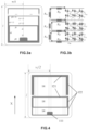
- FIGS. 3a and 3b are equivalent circuit diagrams of the semiconductor device shown in FIG. 1 .
- the gate pad 11 is disposed in the middle of a first portion among the plurality of first portions located in a middle region of the semiconductor device.
- widths or thicknesses of the plurality of first portions, widths or thicknesses of the plurality of second portions, and lengths of the plurality of emitter segments along the first axis may gradually change.
- the position of the gate pad is not particularly limited in the present invention, and the gate pad may be flexibly disposed at a corner, in the middle of a side edge, or in a middle region of the semiconductor device, thus being compatible with various layout designs.
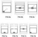
- lengths and positions of the openings on the first portions of the gate busbar may be set according to actual needs.
- the gate pad is located in the middle of a first portion of the gate busbar, and the opening is located in another first portion other than the first portion where the gate pad is located, opposite to the location of the gate pad, i.e., the location of the gate pad is aligned with the location of the opening along the first axis.
- the location of the gate pad is aligned with the location of the opening along the first axis.
- lengths d of the plurality of emitter segments 14 along the first axis A1 change with distances of the plurality of emitter segments 14 from the gate pad 11. Lengths d of the plurality of emitter segments 14 along the first axis A1 may be different from each other.
- widths or thicknesses of the plurality of first portions 121 change with distances of the plurality of first portions 121 from the gate pad 11 and differ from each other
- widths or thicknesses of the plurality of second portions 122 change with distances of the plurality of second portions 122 from the gate pad 11 and differ from each other.
- lengths of the plurality of first portions 121 may be the same.
- V denotes the voltage of the gate busbar while v denotes the voltage of the trench gate.
- Va(i+i) denotes the voltage of the (i+1) th second portion in the first direction
- V ⁇ i denotes the voltage of the first portion (i.e., the i th first portion) connected to an end of the i th second portion away from the gate pad
- v ⁇ (i + 1) denotes the voltage of the trench gate from the i th first portion to the gate between the i th first portion and the (i+1) th first portion
- v ⁇ (i + 1) denotes the voltage of the trench gate from the (i+1) th first portion to the gate between the i th first portion and the (i+1) th first portion.
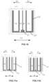
- FIGS. 11a and 11b are schematic diagrams of another semiconductor device according to the second embodiment of the present invention.
- FIG. 11a in a first direction pointing from the gate pad 11 toward a side away from the gate pad 11 along the first axis A1, widths or thicknesses of the plurality of first portions first decrease and then increase, widths or thicknesses of the plurality of second portions first decrease and then increase, and lengths of the plurality of emitter segments along the first axis first decrease and then increase.
- FIG. 11a in a first direction pointing from the gate pad 11 toward a side away from the gate pad 11 along the first axis A1
- widths or thicknesses of the plurality of first portions first decrease and then increase
- widths or thicknesses of the plurality of second portions first decrease and then increase
- lengths of the plurality of emitter segments along the first axis first decrease and then increase.
- the plurality of second portions 122 are disposed at a first side edge S1 of the semiconductor device, and the gate pad 11 is also disposed in the middle of the first side edge S1.
- the present invention is not limited thereto.
- the gate pad 11 may also be disposed at a corner of the semiconductor device.
- the gate pad is disposed at a corner of the semiconductor device, in connection with and in contact with the leftmost first and second portions.
- the plurality of second portions are disposed in a middle region of the semiconductor device, the gate pad is also disposed in the middle region of the semiconductor device, and the gate pad is aligned with the plurality of second portions along the first axis.
- widths or thicknesses of the plurality of first portions, widths or thicknesses of the plurality of second portions, and lengths of the plurality of emitter segments along the first axis may gradually change.
- FIGS. 12a and 12b in a direction from the gate pad to a side away from the gate pad along the first axis (a direction from the gate pad to the right in FIG. 12a , and directions from the gate pad to the left and to the right in FIG.
- widths or thicknesses of the plurality of first portions, widths or thicknesses of the plurality of second portions, and lengths of the plurality of emitter segments along the first axis gradually decrease, but the present invention is not limited thereto. Widths or thicknesses of the plurality of first portions, widths or thicknesses of the plurality of second portions, and lengths of the plurality of emitter segments along the first axis may also gradually increase, first increase and then decrease, first decrease and then increase, etc., as long as gate signals arriving at the gates of the plurality of cells are substantially consistent.
- the semiconductor device may further include a third portion 123 connected to the plurality of first portions at ends of the plurality of first portions which are not connected to the second portions, and the third portion 123 is disposed along the first axis A1 and located at a second side edge S2 of the semiconductor device.
- an opening may be provided in the third portion 123 to facilitate interconnection between elements in different emitter segments 14, and between an element in the emitter segment 14 and an element at the gate busbar's periphery (e.g., ground metal).
- the third portion 123 may also completely enclose the plurality of emitter segments.
- FIG. 14 is a schematic diagram of a semiconductor device according to a third embodiment of the present invention.
- the semiconductor device includes a gate pad 11, a gate busbar 12 and a plurality of trench gates 13.
- the plurality of trench gates 13 connect the gates (not shown in FIG. 14 ) of a plurality of cells of the semiconductor device.
- Each of the trench gates 13 is disposed along a first axis A1.
- the gate busbar 12 includes a plurality of first portions 121 each disposed along a second axis A2.
- the plurality of first portions 121 are connected to the plurality of trench gates 13.
- the first axis A1 intersects with the second axis A2. Similar to the second embodiment shown in FIG.
- the gate pad 11 is disposed along the first axis A1.
- the gate busbar 12 further includes a second portion 122 disposed along the first axis A1.
- the second portion 122 connects the plurality of first portions 121 to the gate pad 11.
- the plurality of first portions 121 are spaced apart from each other to divide the semiconductor device into a plurality of emitter segments 14.
- each of the first portions 121 includes a plurality of first sub-portions 1211 disposed along the second axis A2 and connected in sequence, and at least one of widths, thicknesses and lengths of the plurality of first sub-portions 1211 change along the second axis.
- lengths of the plurality of emitter segments 14 along the first axis A1 may also change with distances of the plurality of emitter segments 14 from the gate pad 11.
- lengths of the emitter segments along the first axis and the width/thickness of each of the first portions of the gate busbar are designed to ensure that each cell could receive a substantially consistent gate signal.
- the gate signal difference between the respective cells could be reduced, no matter how far the cells are from the gate pad, which improves the current sharing capability of the chip.
- the length direction of the semiconductor device is parallel to the second axis A2, and the width direction of the semiconductor device is parallel to the first axis A1.
- widths or thicknesses of the plurality of first sub-portions 1211 gradually change and differ from each other, and lengths of the plurality of first sub-portions 1211 gradually change and differ from each other.
- widths or thicknesses of the plurality of first sub-portions 1211 gradually decrease, and lengths of the plurality of first sub-portions 1211 gradually decrease.
- V denotes the voltage of the gate busbar while v denotes the voltage of the trench gate.
- V ⁇ i denotes the voltage of the i th first sub-portion in the second direction
- V 0 denotes the voltage of the second sub-portion between adjacent first sub-portions
- v ⁇ x and v ⁇ x denote the voltages of the trench gates from two adjacent first sub-portions to the gate therebetween, respectively.
- FIG. 16 is a schematic diagram of another semiconductor device according to the third embodiment of the present invention. As shown in FIG. 16 , in a second direction Y parallel to the second axis A2 and pointing toward a side away from the gate pad 11, widths or thicknesses of the plurality of first sub-portions 1211 gradually increase, and lengths of the plurality of first sub-portions 1211 gradually increase.
- FIGS. 17a and 17b are schematic diagrams of another semiconductor device according to the third embodiment of the present invention.
- FIG. 17a in a second direction Y parallel to the second axis A2 and pointing toward a side away from the gate pad 11, widths or thicknesses of the plurality of first sub-portions 1211 first decrease and then increase, and lengths of the plurality of first sub-portions 1211 first decrease and then increase.
- FIG. 17b in the second direction Y parallel to the second axis A2 and pointing toward a side away from the gate pad 11, widths or thicknesses of the plurality of first sub-portions 1211 first increase and then decrease, and lengths of the plurality of first sub-portions 1211 first increase and then decrease.
- the second portion 122 is disposed at a first side edge S1 of the semiconductor device, and the gate pad 11 is also disposed in the middle of the first side edge S1.
- the present invention is not limited thereto.
- the gate pad 11 may also be disposed at a corner of the semiconductor device.
- the gate pad is disposed at a corner of the semiconductor device, for which the gate pad is in connection with and in contact with the second portion and the leftmost first portion.
- the second portion is disposed in a middle region of the semiconductor device, the gate pad is also disposed in the middle region of the semiconductor device, and the gate pad is aligned with the second portion along the first axis.
- widths or thicknesses of the plurality of first sub-portions 1211 gradually change, and lengths of the plurality of first sub-portions 1211 gradually change.
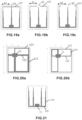
- FIGS. 18a and 18b in a direction from the gate pad 11 to a side away from the gate pad 11 along the second axis A2 (a direction Y upward from the gate pad in FIG. 18a , a direction Y1 upward from the gate pad and a direction Y2 downward from the gate pad in FIG.
- widths or thicknesses of the plurality of first sub-portions 1211 and lengths of the plurality of first sub-portions 1211 gradually decrease, but the present invention is not limited thereto. Widths or thicknesses of the plurality of first sub-portions 1211 and lengths of the plurality of first sub-portions 1211 may gradually increase, first increase and then decrease, first decrease and then increase, etc., as long as gate signals arriving at the gates of the plurality of cells are substantially consistent.
- At least one of widths or thicknesses of the plurality of first sub-portions, lengths of the plurality of first sub-portions, and lengths of the plurality of emitter segments along the first axis may be reasonably designed so that gate signals arriving at the gates of the plurality of cells are substantially consistent.
- the semiconductor device may further include a third portion 123 connected to the plurality of first portions at ends of the plurality of first portions which are not connected to the second portion, and the third portion 123 is disposed along the first axis A1 and located at a second side edge S2 of the semiconductor device.
- an opening may be provided in the third portion 123 to facilitate interconnection between elements in different emitter segments, and between an element in the emitter segment and an element at the gate busbar's periphery (e.g., ground metal).
- the third portion 123 may also completely enclose the plurality of emitter segments.
- the second portion 122 is disposed in an middle region of the semiconductor device
- the gate pad 11 is also disposed in the middle region of the semiconductor device
- the gate pad 11 is aligned with the second portion 122 along the first axis
- the semiconductor device further includes a third portion 123 connected to the plurality of first portions at both ends of the plurality of first portions which are not connected to the second portions
- the third portion 123 is disposed along the first axis A1 and located at two opposite side edges of the semiconductor device.
- the plurality of emitter segments 14 are defined by the plurality of first portions 121, the second portion 122 and the third portion 123, and the plurality of emitter segments 14 have different lengths along the first axis and different widths along the second axis.
- the gate pad 11 may be disposed in connection with and in contact with only the second portion 122, instead of the first portions 121, as shown in FIG. 21 .
- Gate pad 11 Component(s) Reference numeral(s) Gate pad 11
- Gate busbar 12 First portion 121 First sub-portion 1211 Second portion 122, 122a, 122b Third portion 123
- Emitter segment 14 First axis A1 Second axis A2 First direction X, X1, X2 Second direction Y, Y1, Y2 First side edge S1 Second side edge S2 Third side edge S3 Fourth side edge S4
Landscapes
- Electrodes Of Semiconductors (AREA)
- Semiconductor Integrated Circuits (AREA)
- Design And Manufacture Of Integrated Circuits (AREA)
Priority Applications (1)
| Application Number | Priority Date | Filing Date | Title |
|---|---|---|---|
| EP25168499.9A EP4557363A3 (de) | 2022-12-09 | 2023-12-07 | Halbleiteranordnung |
Applications Claiming Priority (1)
| Application Number | Priority Date | Filing Date | Title |
|---|---|---|---|
| CN202211581689.2A CN115939193B (zh) | 2022-12-09 | 2022-12-09 | 半导体器件 |
Related Child Applications (2)
| Application Number | Title | Priority Date | Filing Date |
|---|---|---|---|
| EP25168499.9A Division EP4557363A3 (de) | 2022-12-09 | 2023-12-07 | Halbleiteranordnung |
| EP25168499.9A Division-Into EP4557363A3 (de) | 2022-12-09 | 2023-12-07 | Halbleiteranordnung |
Publications (3)
| Publication Number | Publication Date |
|---|---|
| EP4394864A2 true EP4394864A2 (de) | 2024-07-03 |
| EP4394864A3 EP4394864A3 (de) | 2024-10-02 |
| EP4394864B1 EP4394864B1 (de) | 2026-02-25 |
Family
ID=86700419
Family Applications (3)
| Application Number | Title | Priority Date | Filing Date |
|---|---|---|---|
| EP23214962.5A Pending EP4391045A1 (de) | 2022-12-09 | 2023-12-07 | Halbleiteranordnung |
| EP23214951.8A Active EP4394864B1 (de) | 2022-12-09 | 2023-12-07 | Halbleiteranordnung |
| EP25168499.9A Pending EP4557363A3 (de) | 2022-12-09 | 2023-12-07 | Halbleiteranordnung |
Family Applications Before (1)
| Application Number | Title | Priority Date | Filing Date |
|---|---|---|---|
| EP23214962.5A Pending EP4391045A1 (de) | 2022-12-09 | 2023-12-07 | Halbleiteranordnung |
Family Applications After (1)
| Application Number | Title | Priority Date | Filing Date |
|---|---|---|---|
| EP25168499.9A Pending EP4557363A3 (de) | 2022-12-09 | 2023-12-07 | Halbleiteranordnung |
Country Status (3)
| Country | Link |
|---|---|
| US (2) | US20240194600A1 (de) |
| EP (3) | EP4391045A1 (de) |
| CN (2) | CN115939193B (de) |
Families Citing this family (1)
| Publication number | Priority date | Publication date | Assignee | Title |
|---|---|---|---|---|
| CN121262869A (zh) * | 2025-12-05 | 2026-01-02 | 中国电力科学研究院有限公司 | 一种树状仿生栅极结构、功率半导体芯片 |
Citations (1)
| Publication number | Priority date | Publication date | Assignee | Title |
|---|---|---|---|---|
| CN114220853A (zh) | 2021-12-15 | 2022-03-22 | 株洲中车时代半导体有限公司 | 功率芯片 |
Family Cites Families (6)
| Publication number | Priority date | Publication date | Assignee | Title |
|---|---|---|---|---|
| JP5777319B2 (ja) * | 2010-10-27 | 2015-09-09 | 三菱電機株式会社 | 半導体装置 |
| JP6440989B2 (ja) * | 2013-08-28 | 2018-12-19 | ローム株式会社 | 半導体装置 |
| KR101745776B1 (ko) * | 2015-05-12 | 2017-06-28 | 매그나칩 반도체 유한회사 | 전력용 반도체 소자 |
| JP6681238B2 (ja) * | 2016-03-28 | 2020-04-15 | ローム株式会社 | 半導体装置および半導体装置の製造方法 |
| CN112687654B (zh) * | 2020-12-14 | 2024-02-23 | 株洲中车时代半导体有限公司 | 沟槽栅igbt器件 |
| US11664436B2 (en) * | 2021-03-01 | 2023-05-30 | Wolfspeed, Inc. | Semiconductor devices having gate resistors with low variation in resistance values |
-
2022
- 2022-12-09 CN CN202211581689.2A patent/CN115939193B/zh active Active
- 2022-12-09 CN CN202311344782.6A patent/CN118173586A/zh active Pending
-
2023
- 2023-12-07 EP EP23214962.5A patent/EP4391045A1/de active Pending
- 2023-12-07 EP EP23214951.8A patent/EP4394864B1/de active Active
- 2023-12-07 EP EP25168499.9A patent/EP4557363A3/de active Pending
- 2023-12-08 US US18/533,460 patent/US20240194600A1/en active Pending
- 2023-12-08 US US18/533,437 patent/US20240194599A1/en active Pending
Patent Citations (1)
| Publication number | Priority date | Publication date | Assignee | Title |
|---|---|---|---|---|
| CN114220853A (zh) | 2021-12-15 | 2022-03-22 | 株洲中车时代半导体有限公司 | 功率芯片 |
Also Published As
| Publication number | Publication date |
|---|---|
| CN115939193B (zh) | 2023-11-03 |
| EP4557363A3 (de) | 2025-09-10 |
| US20240194599A1 (en) | 2024-06-13 |
| EP4394864A3 (de) | 2024-10-02 |
| EP4394864B1 (de) | 2026-02-25 |
| CN118173586A (zh) | 2024-06-11 |
| EP4557363A2 (de) | 2025-05-21 |
| CN115939193A (zh) | 2023-04-07 |
| EP4391045A1 (de) | 2024-06-26 |
| US20240194600A1 (en) | 2024-06-13 |
Similar Documents
| Publication | Publication Date | Title |
|---|---|---|
| US20240153955A1 (en) | Semiconductor device | |
| US6376890B1 (en) | High-voltage edge termination for planar structures | |
| US8178941B2 (en) | Semiconductor device | |
| US20090152624A1 (en) | Integrated circuit device with a semiconductor body and method for the production of an integrated circuit device | |
| US10566448B2 (en) | Insulated gate bipolar transistor | |
| US8530964B2 (en) | Semiconductor device including first and second semiconductor elements | |
| US11164813B2 (en) | Transistor semiconductor die with increased active area | |
| US10868170B2 (en) | Layout for needle cell trench MOSFET | |
| US11545561B2 (en) | Methods for manufacturing a MOSFET | |
| US6037631A (en) | Semiconductor component with a high-voltage endurance edge structure | |
| EP4394864A2 (de) | Halbleiteranordnung | |
| EP3686929A1 (de) | Halbleiterchip | |
| US20240421199A1 (en) | Semiconductor device | |
| US8772861B2 (en) | Field effect trench transistor having active trenches | |
| US6992351B2 (en) | Semiconductor device for power MOS transistor module | |
| EP0557126A1 (de) | Leistungshalbleiteranordnung | |
| US7619280B2 (en) | Current sense trench type MOSFET with improved accuracy and ESD withstand capability | |
| US7253474B2 (en) | Quasi-vertical semiconductor component | |
| US20020167044A1 (en) | Semiconductor component with an edge termination that is suitable for high voltage | |
| US20240113053A1 (en) | Semiconductor device and method of producing thereof | |
| TWI907159B (zh) | 半導體裝置 | |
| US20250351555A1 (en) | Semiconductor device | |
| EP1733424B1 (de) | Halbleitervorrichtung | |
| US20250212526A1 (en) | Trench electrostatic discharge protection device | |
| US12243869B2 (en) | Semiconductor device and semiconductor storage device |
Legal Events
| Date | Code | Title | Description |
|---|---|---|---|
| PUAI | Public reference made under article 153(3) epc to a published international application that has entered the european phase |
Free format text: ORIGINAL CODE: 0009012 |
|
| STAA | Information on the status of an ep patent application or granted ep patent |
Free format text: STATUS: THE APPLICATION HAS BEEN PUBLISHED |
|
| AK | Designated contracting states |
Kind code of ref document: A2 Designated state(s): AL AT BE BG CH CY CZ DE DK EE ES FI FR GB GR HR HU IE IS IT LI LT LU LV MC ME MK MT NL NO PL PT RO RS SE SI SK SM TR |
|
| PUAL | Search report despatched |
Free format text: ORIGINAL CODE: 0009013 |
|
| RIC1 | Information provided on ipc code assigned before grant |
Ipc: H01L 23/482 20060101AFI20240821BHEP |
|
| AK | Designated contracting states |
Kind code of ref document: A3 Designated state(s): AL AT BE BG CH CY CZ DE DK EE ES FI FR GB GR HR HU IE IS IT LI LT LU LV MC ME MK MT NL NO PL PT RO RS SE SI SK SM TR |
|
| STAA | Information on the status of an ep patent application or granted ep patent |
Free format text: STATUS: REQUEST FOR EXAMINATION WAS MADE |
|
| 17P | Request for examination filed |
Effective date: 20250402 |
|
| GRAP | Despatch of communication of intention to grant a patent |
Free format text: ORIGINAL CODE: EPIDOSNIGR1 |
|
| STAA | Information on the status of an ep patent application or granted ep patent |
Free format text: STATUS: GRANT OF PATENT IS INTENDED |
|
| INTG | Intention to grant announced |
Effective date: 20250925 |
|
| GRAS | Grant fee paid |
Free format text: ORIGINAL CODE: EPIDOSNIGR3 |
|
| GRAA | (expected) grant |
Free format text: ORIGINAL CODE: 0009210 |
|
| STAA | Information on the status of an ep patent application or granted ep patent |
Free format text: STATUS: THE PATENT HAS BEEN GRANTED |
|
| AK | Designated contracting states |
Kind code of ref document: B1 Designated state(s): AL AT BE BG CH CY CZ DE DK EE ES FI FR GB GR HR HU IE IS IT LI LT LU LV MC ME MK MT NL NO PL PT RO RS SE SI SK SM TR |
|
| REG | Reference to a national code |
Ref country code: CH Ref legal event code: F10 Free format text: ST27 STATUS EVENT CODE: U-0-0-F10-F00 (AS PROVIDED BY THE NATIONAL OFFICE) Effective date: 20260225 Ref country code: GB Ref legal event code: FG4D |
|
| REG | Reference to a national code |
Ref country code: DE Ref legal event code: R096 Ref document number: 602023012572 Country of ref document: DE |
|
| REG | Reference to a national code |
Ref country code: IE Ref legal event code: FG4D |