EP4394826A2 - Multilayer electronic component - Google Patents
Multilayer electronic component Download PDFInfo
- Publication number
- EP4394826A2 EP4394826A2 EP23216218.0A EP23216218A EP4394826A2 EP 4394826 A2 EP4394826 A2 EP 4394826A2 EP 23216218 A EP23216218 A EP 23216218A EP 4394826 A2 EP4394826 A2 EP 4394826A2
- Authority
- EP
- European Patent Office
- Prior art keywords
- core
- core portion
- dielectric
- electronic component
- multilayer electronic
- Prior art date
- Legal status (The legal status is an assumption and is not a legal conclusion. Google has not performed a legal analysis and makes no representation as to the accuracy of the status listed.)
- Pending
Links
Images



Classifications
-
- H—ELECTRICITY
- H01—ELECTRIC ELEMENTS
- H01G—CAPACITORS; CAPACITORS, RECTIFIERS, DETECTORS, SWITCHING DEVICES, LIGHT-SENSITIVE OR TEMPERATURE-SENSITIVE DEVICES OF THE ELECTROLYTIC TYPE
- H01G4/00—Fixed capacitors; Processes of their manufacture
- H01G4/002—Details
- H01G4/018—Dielectrics
- H01G4/06—Solid dielectrics
- H01G4/08—Inorganic dielectrics
- H01G4/12—Ceramic dielectrics
- H01G4/1209—Ceramic dielectrics characterised by the ceramic dielectric material
- H01G4/1218—Ceramic dielectrics characterised by the ceramic dielectric material based on titanium oxides or titanates
-
- C—CHEMISTRY; METALLURGY
- C04—CEMENTS; CONCRETE; ARTIFICIAL STONE; CERAMICS; REFRACTORIES
- C04B—LIME, MAGNESIA; SLAG; CEMENTS; COMPOSITIONS THEREOF, e.g. MORTARS, CONCRETE OR LIKE BUILDING MATERIALS; ARTIFICIAL STONE; CERAMICS; REFRACTORIES; TREATMENT OF NATURAL STONE
- C04B35/00—Shaped ceramic products characterised by their composition; Ceramics compositions; Processing powders of inorganic compounds preparatory to the manufacturing of ceramic products
- C04B35/01—Shaped ceramic products characterised by their composition; Ceramics compositions; Processing powders of inorganic compounds preparatory to the manufacturing of ceramic products based on oxide ceramics
- C04B35/46—Shaped ceramic products characterised by their composition; Ceramics compositions; Processing powders of inorganic compounds preparatory to the manufacturing of ceramic products based on oxide ceramics based on titanium oxides or titanates
- C04B35/462—Shaped ceramic products characterised by their composition; Ceramics compositions; Processing powders of inorganic compounds preparatory to the manufacturing of ceramic products based on oxide ceramics based on titanium oxides or titanates based on titanates
- C04B35/465—Shaped ceramic products characterised by their composition; Ceramics compositions; Processing powders of inorganic compounds preparatory to the manufacturing of ceramic products based on oxide ceramics based on titanium oxides or titanates based on titanates based on alkaline earth metal titanates
- C04B35/468—Shaped ceramic products characterised by their composition; Ceramics compositions; Processing powders of inorganic compounds preparatory to the manufacturing of ceramic products based on oxide ceramics based on titanium oxides or titanates based on titanates based on alkaline earth metal titanates based on barium titanates
- C04B35/4682—Shaped ceramic products characterised by their composition; Ceramics compositions; Processing powders of inorganic compounds preparatory to the manufacturing of ceramic products based on oxide ceramics based on titanium oxides or titanates based on titanates based on alkaline earth metal titanates based on barium titanates based on BaTiO3 perovskite phase
-
- C—CHEMISTRY; METALLURGY
- C04—CEMENTS; CONCRETE; ARTIFICIAL STONE; CERAMICS; REFRACTORIES
- C04B—LIME, MAGNESIA; SLAG; CEMENTS; COMPOSITIONS THEREOF, e.g. MORTARS, CONCRETE OR LIKE BUILDING MATERIALS; ARTIFICIAL STONE; CERAMICS; REFRACTORIES; TREATMENT OF NATURAL STONE
- C04B35/00—Shaped ceramic products characterised by their composition; Ceramics compositions; Processing powders of inorganic compounds preparatory to the manufacturing of ceramic products
- C04B35/01—Shaped ceramic products characterised by their composition; Ceramics compositions; Processing powders of inorganic compounds preparatory to the manufacturing of ceramic products based on oxide ceramics
- C04B35/46—Shaped ceramic products characterised by their composition; Ceramics compositions; Processing powders of inorganic compounds preparatory to the manufacturing of ceramic products based on oxide ceramics based on titanium oxides or titanates
- C04B35/462—Shaped ceramic products characterised by their composition; Ceramics compositions; Processing powders of inorganic compounds preparatory to the manufacturing of ceramic products based on oxide ceramics based on titanium oxides or titanates based on titanates
- C04B35/465—Shaped ceramic products characterised by their composition; Ceramics compositions; Processing powders of inorganic compounds preparatory to the manufacturing of ceramic products based on oxide ceramics based on titanium oxides or titanates based on titanates based on alkaline earth metal titanates
- C04B35/47—Shaped ceramic products characterised by their composition; Ceramics compositions; Processing powders of inorganic compounds preparatory to the manufacturing of ceramic products based on oxide ceramics based on titanium oxides or titanates based on titanates based on alkaline earth metal titanates based on strontium titanates
-
- C—CHEMISTRY; METALLURGY
- C04—CEMENTS; CONCRETE; ARTIFICIAL STONE; CERAMICS; REFRACTORIES
- C04B—LIME, MAGNESIA; SLAG; CEMENTS; COMPOSITIONS THEREOF, e.g. MORTARS, CONCRETE OR LIKE BUILDING MATERIALS; ARTIFICIAL STONE; CERAMICS; REFRACTORIES; TREATMENT OF NATURAL STONE
- C04B35/00—Shaped ceramic products characterised by their composition; Ceramics compositions; Processing powders of inorganic compounds preparatory to the manufacturing of ceramic products
- C04B35/01—Shaped ceramic products characterised by their composition; Ceramics compositions; Processing powders of inorganic compounds preparatory to the manufacturing of ceramic products based on oxide ceramics
- C04B35/48—Shaped ceramic products characterised by their composition; Ceramics compositions; Processing powders of inorganic compounds preparatory to the manufacturing of ceramic products based on oxide ceramics based on zirconium or hafnium oxides, zirconates, zircon or hafnates
- C04B35/49—Shaped ceramic products characterised by their composition; Ceramics compositions; Processing powders of inorganic compounds preparatory to the manufacturing of ceramic products based on oxide ceramics based on zirconium or hafnium oxides, zirconates, zircon or hafnates containing also titanium oxides or titanates
-
- C—CHEMISTRY; METALLURGY
- C04—CEMENTS; CONCRETE; ARTIFICIAL STONE; CERAMICS; REFRACTORIES
- C04B—LIME, MAGNESIA; SLAG; CEMENTS; COMPOSITIONS THEREOF, e.g. MORTARS, CONCRETE OR LIKE BUILDING MATERIALS; ARTIFICIAL STONE; CERAMICS; REFRACTORIES; TREATMENT OF NATURAL STONE
- C04B35/00—Shaped ceramic products characterised by their composition; Ceramics compositions; Processing powders of inorganic compounds preparatory to the manufacturing of ceramic products
- C04B35/622—Forming processes; Processing powders of inorganic compounds preparatory to the manufacturing of ceramic products
- C04B35/626—Preparing or treating the powders individually or as batches ; preparing or treating macroscopic reinforcing agents for ceramic products, e.g. fibres; mechanical aspects section B
- C04B35/628—Coating the powders or the macroscopic reinforcing agents
- C04B35/62802—Powder coating materials
- C04B35/62805—Oxide ceramics
- C04B35/62815—Rare earth metal oxides
-
- C—CHEMISTRY; METALLURGY
- C04—CEMENTS; CONCRETE; ARTIFICIAL STONE; CERAMICS; REFRACTORIES
- C04B—LIME, MAGNESIA; SLAG; CEMENTS; COMPOSITIONS THEREOF, e.g. MORTARS, CONCRETE OR LIKE BUILDING MATERIALS; ARTIFICIAL STONE; CERAMICS; REFRACTORIES; TREATMENT OF NATURAL STONE
- C04B35/00—Shaped ceramic products characterised by their composition; Ceramics compositions; Processing powders of inorganic compounds preparatory to the manufacturing of ceramic products
- C04B35/622—Forming processes; Processing powders of inorganic compounds preparatory to the manufacturing of ceramic products
- C04B35/626—Preparing or treating the powders individually or as batches ; preparing or treating macroscopic reinforcing agents for ceramic products, e.g. fibres; mechanical aspects section B
- C04B35/628—Coating the powders or the macroscopic reinforcing agents
- C04B35/62802—Powder coating materials
- C04B35/62805—Oxide ceramics
- C04B35/62818—Refractory metal oxides
- C04B35/62823—Zirconium or hafnium oxide
-
- C—CHEMISTRY; METALLURGY
- C04—CEMENTS; CONCRETE; ARTIFICIAL STONE; CERAMICS; REFRACTORIES
- C04B—LIME, MAGNESIA; SLAG; CEMENTS; COMPOSITIONS THEREOF, e.g. MORTARS, CONCRETE OR LIKE BUILDING MATERIALS; ARTIFICIAL STONE; CERAMICS; REFRACTORIES; TREATMENT OF NATURAL STONE
- C04B35/00—Shaped ceramic products characterised by their composition; Ceramics compositions; Processing powders of inorganic compounds preparatory to the manufacturing of ceramic products
- C04B35/622—Forming processes; Processing powders of inorganic compounds preparatory to the manufacturing of ceramic products
- C04B35/626—Preparing or treating the powders individually or as batches ; preparing or treating macroscopic reinforcing agents for ceramic products, e.g. fibres; mechanical aspects section B
- C04B35/628—Coating the powders or the macroscopic reinforcing agents
- C04B35/62894—Coating the powders or the macroscopic reinforcing agents with more than one coating layer
-
- C—CHEMISTRY; METALLURGY
- C04—CEMENTS; CONCRETE; ARTIFICIAL STONE; CERAMICS; REFRACTORIES
- C04B—LIME, MAGNESIA; SLAG; CEMENTS; COMPOSITIONS THEREOF, e.g. MORTARS, CONCRETE OR LIKE BUILDING MATERIALS; ARTIFICIAL STONE; CERAMICS; REFRACTORIES; TREATMENT OF NATURAL STONE
- C04B35/00—Shaped ceramic products characterised by their composition; Ceramics compositions; Processing powders of inorganic compounds preparatory to the manufacturing of ceramic products
- C04B35/622—Forming processes; Processing powders of inorganic compounds preparatory to the manufacturing of ceramic products
- C04B35/626—Preparing or treating the powders individually or as batches ; preparing or treating macroscopic reinforcing agents for ceramic products, e.g. fibres; mechanical aspects section B
- C04B35/628—Coating the powders or the macroscopic reinforcing agents
- C04B35/62897—Coatings characterised by their thickness
-
- H—ELECTRICITY
- H01—ELECTRIC ELEMENTS
- H01G—CAPACITORS; CAPACITORS, RECTIFIERS, DETECTORS, SWITCHING DEVICES, LIGHT-SENSITIVE OR TEMPERATURE-SENSITIVE DEVICES OF THE ELECTROLYTIC TYPE
- H01G4/00—Fixed capacitors; Processes of their manufacture
- H01G4/002—Details
- H01G4/005—Electrodes
- H01G4/012—Form of non-self-supporting electrodes
-
- H—ELECTRICITY
- H01—ELECTRIC ELEMENTS
- H01G—CAPACITORS; CAPACITORS, RECTIFIERS, DETECTORS, SWITCHING DEVICES, LIGHT-SENSITIVE OR TEMPERATURE-SENSITIVE DEVICES OF THE ELECTROLYTIC TYPE
- H01G4/00—Fixed capacitors; Processes of their manufacture
- H01G4/002—Details
- H01G4/018—Dielectrics
- H01G4/06—Solid dielectrics
- H01G4/08—Inorganic dielectrics
- H01G4/12—Ceramic dielectrics
- H01G4/1209—Ceramic dielectrics characterised by the ceramic dielectric material
- H01G4/1218—Ceramic dielectrics characterised by the ceramic dielectric material based on titanium oxides or titanates
- H01G4/1227—Ceramic dielectrics characterised by the ceramic dielectric material based on titanium oxides or titanates based on alkaline earth titanates
-
- H—ELECTRICITY
- H01—ELECTRIC ELEMENTS
- H01G—CAPACITORS; CAPACITORS, RECTIFIERS, DETECTORS, SWITCHING DEVICES, LIGHT-SENSITIVE OR TEMPERATURE-SENSITIVE DEVICES OF THE ELECTROLYTIC TYPE
- H01G4/00—Fixed capacitors; Processes of their manufacture
- H01G4/002—Details
- H01G4/228—Terminals
- H01G4/232—Terminals electrically connecting two or more layers of a stacked or rolled capacitor
- H01G4/2325—Terminals electrically connecting two or more layers of a stacked or rolled capacitor characterised by the material of the terminals
-
- H—ELECTRICITY
- H01—ELECTRIC ELEMENTS
- H01G—CAPACITORS; CAPACITORS, RECTIFIERS, DETECTORS, SWITCHING DEVICES, LIGHT-SENSITIVE OR TEMPERATURE-SENSITIVE DEVICES OF THE ELECTROLYTIC TYPE
- H01G4/00—Fixed capacitors; Processes of their manufacture
- H01G4/30—Stacked capacitors
-
- C—CHEMISTRY; METALLURGY
- C04—CEMENTS; CONCRETE; ARTIFICIAL STONE; CERAMICS; REFRACTORIES
- C04B—LIME, MAGNESIA; SLAG; CEMENTS; COMPOSITIONS THEREOF, e.g. MORTARS, CONCRETE OR LIKE BUILDING MATERIALS; ARTIFICIAL STONE; CERAMICS; REFRACTORIES; TREATMENT OF NATURAL STONE
- C04B2235/00—Aspects relating to ceramic starting mixtures or sintered ceramic products
- C04B2235/02—Composition of constituents of the starting material or of secondary phases of the final product
- C04B2235/30—Constituents and secondary phases not being of a fibrous nature
- C04B2235/32—Metal oxides, mixed metal oxides, or oxide-forming salts thereof, e.g. carbonates, nitrates, (oxy)hydroxides, chlorides
- C04B2235/3205—Alkaline earth oxides or oxide forming salts thereof, e.g. beryllium oxide
- C04B2235/3208—Calcium oxide or oxide-forming salts thereof, e.g. lime
-
- C—CHEMISTRY; METALLURGY
- C04—CEMENTS; CONCRETE; ARTIFICIAL STONE; CERAMICS; REFRACTORIES
- C04B—LIME, MAGNESIA; SLAG; CEMENTS; COMPOSITIONS THEREOF, e.g. MORTARS, CONCRETE OR LIKE BUILDING MATERIALS; ARTIFICIAL STONE; CERAMICS; REFRACTORIES; TREATMENT OF NATURAL STONE
- C04B2235/00—Aspects relating to ceramic starting mixtures or sintered ceramic products
- C04B2235/02—Composition of constituents of the starting material or of secondary phases of the final product
- C04B2235/30—Constituents and secondary phases not being of a fibrous nature
- C04B2235/32—Metal oxides, mixed metal oxides, or oxide-forming salts thereof, e.g. carbonates, nitrates, (oxy)hydroxides, chlorides
- C04B2235/3205—Alkaline earth oxides or oxide forming salts thereof, e.g. beryllium oxide
- C04B2235/3215—Barium oxides or oxide-forming salts thereof
-
- C—CHEMISTRY; METALLURGY
- C04—CEMENTS; CONCRETE; ARTIFICIAL STONE; CERAMICS; REFRACTORIES
- C04B—LIME, MAGNESIA; SLAG; CEMENTS; COMPOSITIONS THEREOF, e.g. MORTARS, CONCRETE OR LIKE BUILDING MATERIALS; ARTIFICIAL STONE; CERAMICS; REFRACTORIES; TREATMENT OF NATURAL STONE
- C04B2235/00—Aspects relating to ceramic starting mixtures or sintered ceramic products
- C04B2235/70—Aspects relating to sintered or melt-casted ceramic products
- C04B2235/74—Physical characteristics
- C04B2235/76—Crystal structural characteristics, e.g. symmetry
- C04B2235/768—Perovskite structure ABO3
-
- C—CHEMISTRY; METALLURGY
- C04—CEMENTS; CONCRETE; ARTIFICIAL STONE; CERAMICS; REFRACTORIES
- C04B—LIME, MAGNESIA; SLAG; CEMENTS; COMPOSITIONS THEREOF, e.g. MORTARS, CONCRETE OR LIKE BUILDING MATERIALS; ARTIFICIAL STONE; CERAMICS; REFRACTORIES; TREATMENT OF NATURAL STONE
- C04B2235/00—Aspects relating to ceramic starting mixtures or sintered ceramic products
- C04B2235/70—Aspects relating to sintered or melt-casted ceramic products
- C04B2235/74—Physical characteristics
- C04B2235/78—Grain sizes and shapes, product microstructures, e.g. acicular grains, equiaxed grains, platelet-structures
- C04B2235/785—Submicron sized grains, i.e. from 0,1 to 1 micron
-
- C—CHEMISTRY; METALLURGY
- C04—CEMENTS; CONCRETE; ARTIFICIAL STONE; CERAMICS; REFRACTORIES
- C04B—LIME, MAGNESIA; SLAG; CEMENTS; COMPOSITIONS THEREOF, e.g. MORTARS, CONCRETE OR LIKE BUILDING MATERIALS; ARTIFICIAL STONE; CERAMICS; REFRACTORIES; TREATMENT OF NATURAL STONE
- C04B2235/00—Aspects relating to ceramic starting mixtures or sintered ceramic products
- C04B2235/70—Aspects relating to sintered or melt-casted ceramic products
- C04B2235/80—Phases present in the sintered or melt-cast ceramic products other than the main phase
- C04B2235/85—Intergranular or grain boundary phases
-
- H—ELECTRICITY
- H01—ELECTRIC ELEMENTS
- H01G—CAPACITORS; CAPACITORS, RECTIFIERS, DETECTORS, SWITCHING DEVICES, LIGHT-SENSITIVE OR TEMPERATURE-SENSITIVE DEVICES OF THE ELECTROLYTIC TYPE
- H01G4/00—Fixed capacitors; Processes of their manufacture
- H01G4/002—Details
- H01G4/018—Dielectrics
- H01G4/06—Solid dielectrics
- H01G4/08—Inorganic dielectrics
- H01G4/12—Ceramic dielectrics
- H01G4/1209—Ceramic dielectrics characterised by the ceramic dielectric material
Definitions
- a multilayer electronic component may be a chip condenser mounted on a printed circuit board of various types of electronic products such as imaging devices including a liquid crystal display (LCD) and a plasma display panel (PDP), a computer, a smartphone, and a mobile phone and charging or discharging electricity.
- imaging devices including a liquid crystal display (LCD) and a plasma display panel (PDP), a computer, a smartphone, and a mobile phone and charging or discharging electricity.
- LCD liquid crystal display
- PDP plasma display panel
- a multilayer electronic component includes a body including a dielectric layer and an internal electrode; and external electrodes disposed on the body.
- the dielectric layer includes a plurality of dielectric grains having a perovskite-based composition represented by ABO 3 , the A includes a first element including at least one of Bi, Na, K, Sr, and Ca, and the B includes a second element including Ti.
- At least one of the plurality of dielectric grains has a core-shell structure including a core portion on an internal side and a shell portion covering at least a portion of the core portion, and a content of the first element included in the core portion is twice or more than a content of the first element included in the shell portion.
- the core portion includes a first core portion on an internal side and a second core portion covering at least a portion of the first core portion, and the second core portion includes Zr.
- a first direction may be defined as a lamination direction or a thickness T direction
- a second direction may be defined as a length L direction
- a third direction may be defined as a width W direction.
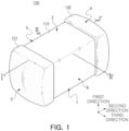
- FIG. 1 is a perspective diagram illustrating a multilayer electronic component according to an example embodiment.
- FIG. 2 is an exploded perspective diagram illustrating a laminate structure of internal electrodes according to an example embodiment.
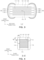
- FIG. 3 is a cross-sectional diagram taken along line I-I' in FIG. 1 .
- FIG. 4 is a cross-sectional diagram taken along line II-II' in FIG. 1 .
- FIG. 5 is an enlarged diagram illustrating region P in FIG. 3 .
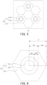
- FIG. 6 is a diagram illustrating a dielectric grain having a core-shell structure according to an example embodiment.
- FIG. 7 is a diagram illustrating a dielectric grain having a core-shell structure according to an example embodiment.
- FIG. 8 is a diagram illustrating an element content (mass percentage) for each region of a dielectric grain having a core-shell structure according to an example embodiment.
- a multilayer electronic component according to an example embodiment will be described in greater detail with reference to FIGS. 1 to 8 .
- a multilayer ceramic capacitor will be described as an example of a multilayer electronic component, but the example embodiment may also be applied to various electronic products using a dielectric composition, such as an inductor, a piezoelectric element, a varistor, or a thermistor.
- a multilayer electronic component 100 may include a body 110 including a dielectric layer 111 and internal electrodes 121 and 122; and external electrodes 131 and 132 disposed on the body 110.
- the dielectric layer 111 may include a plurality of dielectric grains having a perovskite-based composition represented by ABO 3
- the A may include a first element including at least one of Bi, Na, K, Sr, and Ca
- the B may include a second element including Ti
- at least one of the plurality of dielectric grains may include a core-shell structure 20 including a core portion 21 on an internal side and a shell portion 22 covering at least a portion of the core portion 21, the content of the first element included in the core portion 21 may be twice or more than the content of the first element included in the shell portion 22,
- the core portion 21 may include a first core portion 21a on an internal side and a second core portion 21b covering at least a portion of the first core portion 21a
- the second core portion 21b may include Zr.
- the dielectric layers 111 and internal electrodes 121 and 122 may be alternately laminated.
- the body 110 may have first and second surfaces 1 and 2 opposing each other in the first direction, third and fourth surfaces 3 and 4 connected to the first and second surfaces 1 and 2 and opposing in the second direction, and fifth and sixth surfaces 5 and 6 connected to the first and second surfaces 1 and 2 and the third and fourth surfaces 3 and 4 and opposing each other in the third direction.
- the plurality of dielectric layers 111 forming the body 110 may be in a sintered state, and a boundary between the adjacent dielectric layers 111 may be integrated with each other such that the boundary may not be distinct without using a scanning electron microscope (SEM).
- SEM scanning electron microscope
- the barium titanate material may include BaTiO 3 ceramic powder, and an example of the ceramic powder may include (Ba 1-x Ca x )TiO 3 (0 ⁇ x ⁇ 1), Ba(Ti 1-y Ca y )O 3 (0 ⁇ y ⁇ 1), (Ba 1-x Ca x )(Ti 1-y Zr y )O 3 (0 ⁇ x ⁇ 1, 0 ⁇ y ⁇ 1) or Ba(Ti 1-y Zr y )O 3 (0 ⁇ y ⁇ 1) in which Ca (calcium), Zr (zirconium) is partially solid-solute.
- various ceramic additives, organic solvents, binders, dispersants, or the like may be added to a raw material for forming the dielectric layer 111 in the example embodiment to powder such as barium titanate (BaTiO 3 ).
- the A-site in the ABO 3 perovskite-based composition may include a first element including at least one of Bi, Na, K, Sr, and Ca.
- the B-site may include a second element including Ti, but an example embodiment thereof is not limited thereto, and may include at least one element of Hf and Zr.
- the A-site of the ABO 3 perovskite-based composition may include a first element including at least one of Bi, Na, K, Sr, and Ca, and the B-site may include a second element including at least one of Ti, Hf, and Zr, such that degradation of dielectric properties due to DC-bias properties may be effectively prevented even under high-temperature/high-voltage conditions, thereby manufacturing a multilayer electronic component having improved reliability.
- the content of the first element may be 80 mol% or more based on 100 mol% of the A-site element
- the content of the second element may be 80 mol% or more based on 100 mol% of the B-site element.
- Dc-bias properties may be improved, and by including 80 mol% or more of the second element based on 100 mol% of the B element, the effect of improvement in reliability may be excellent.
- an average value may be calculated by measuring 5 or more points on the core portion 21 and 10 or more points on the shell portion 22, and the first element content of the entirety of pixels may be measured by mapping the first element, and the content of the first element included in each region may be calculated from the first element content of the entirety of pixels.
- the effect of improvement of the Dc-bias properties may decrease, but when the fraction of the shell portion 22 is determined to be low, it may be difficult to form a uniform and stable shell portion 22, such that it may be difficult to expect the effect of improvement in dielectric properties to be supplemented, particularly the effect of improvement in reliability.
- insulation resistance may be increased, and the fraction of the shell portion 22 may be stably reduced and may be formed uniformly, such that dielectric properties may be supplemented while improving insulation resistance properties.
- the method of forming the zirconium (Zr) substitution layer is not limited to any particular example, and by coating and pre-diffusing zirconium (Zr) on the ABO 3 base material powder before sintering, zirconium (Zr) may be diffused into the core portion 21, and a second core portion 21b including zirconium (Zr) in the dielectric grain 20 of the core-shell structure may be formed.
- the linear distance from the central point A1 of the dielectric grain 20' of the core-shell structure to the grain boundary A4 is defined as DL
- the linear distance from the central point A1 of the dielectric grain 20' of the core-shell structure to the boundary point A3 of the core portion 21' and shell portion 22' is defined as D1
- the linear distance from the boundary point A3 of the core portion 21' and the shell portion 22' to the grain boundary A4 is defined as D2
- the linear distance from the central point A1 of the dielectric grain 20' of the core-shell structure to the central point A2 of the core portion 21' is defined as D3, 0 ⁇ D3 and D2 ⁇ D1 may be satisfied.
- the thickness td of the dielectric layer 111 may refer to the size of the dielectric layer 111 in the first direction. Also, the thickness td of the dielectric layer 111 may refer to the average thickness td of the dielectric layer 111 and may refer to the average size of the dielectric layer 111 in the first direction.
- the resin included in the second electrode layers 131b and 132b may secure bonding and may absorb impacts.
- the resin included in the second electrode layers 131b and 132b is not limited to any particular example as long as the resin may have bondability and shock absorption and may be mixed with conductive metal powder and may form a paste, and may include, for example, an epoxy resin.
- the plating layers 131c and 132c may improve mounting properties.
- the plating layers 131c and 132c may be Ni plating layers or Sn plating layers, and Ni plating layers and Sn plating layers may be formed in order on the electrode layers 131a, 132a, 131b, and 132b, and a Sn plating layer, a Ni plating layer, and a Sn plating layer may be formed in order.
- the plating layers 131c and 132c may include a plurality of Ni plating layers and/or a plurality of Sn plating layers.
Landscapes
- Engineering & Computer Science (AREA)
- Chemical & Material Sciences (AREA)
- Power Engineering (AREA)
- Ceramic Engineering (AREA)
- Manufacturing & Machinery (AREA)
- Microelectronics & Electronic Packaging (AREA)
- Inorganic Chemistry (AREA)
- Materials Engineering (AREA)
- Structural Engineering (AREA)
- Organic Chemistry (AREA)
- Composite Materials (AREA)
- Fixed Capacitors And Capacitor Manufacturing Machines (AREA)
- Ceramic Capacitors (AREA)
Abstract
Description
- This application claims benefit of priority to
Korean Patent Application No. 10-2022-0184401 filed on December 26, 2022 - The present disclosure relates to a multilayer electronic component.
- A multilayer electronic component (MLCC), a multilayer electronic component, may be a chip condenser mounted on a printed circuit board of various types of electronic products such as imaging devices including a liquid crystal display (LCD) and a plasma display panel (PDP), a computer, a smartphone, and a mobile phone and charging or discharging electricity.
- Such a multilayer ceramic capacitor may be used as a component of various electronic devices as a multilayer ceramic capacitor may have a small size and high capacitance thereof and may be easily mounted. As various electronic devices such as computers and mobile devices have been miniaturized and high-output, demand for miniaturization and high capacitance multilayer ceramic capacitors has been increased.
- Meanwhile, when a high voltage is applied to a barium titanate (BaTiO3)-based multilayer ceramic capacitor, dielectric properties may be significantly reduced due to DC-bias properties. To prevent deterioration of dielectric properties due to high voltage application, by dissolving and diffusing an element other than Ba or Ti into barium titanate and are substituting an elemental site of Ba or Ti, degradation of dielectric properties due to DC-bias properties may be prevented. However, as Ba or Ti elements are substituted, dielectric properties such as a high dielectric constant of existing BaTiO3 may be deteriorated, such that it may be necessary to design the composition appropriately.
- An example embodiment of the present disclosure is to prevent deterioration of dielectric properties of a multilayer electronic component even in a high-temperature/high-pressure environment and to improve reliability.
- According to an example embodiment of the present disclosure, a multilayer electronic component includes a body including a dielectric layer and an internal electrode; and external electrodes disposed on the body. The dielectric layer includes a plurality of dielectric grains having a perovskite-based composition represented by ABO3, the A includes a first element including at least one of Bi, Na, K, Sr, and Ca, and the B includes a second element including Ti. At least one of the plurality of dielectric grains has a core-shell structure including a core portion on an internal side and a shell portion covering at least a portion of the core portion, and a content of the first element included in the core portion is twice or more than a content of the first element included in the shell portion. The core portion includes a first core portion on an internal side and a second core portion covering at least a portion of the first core portion, and the second core portion includes Zr.
- According to an example embodiment of the present disclosure, a multilayer electronic component includes a body including a dielectric layer and an internal electrode; and an external electrode disposed on the body to connect to the internal electrode. The dielectric layer includes a dielectric grain having a core-shell structure including a core portion and a shell portion covering at least a portion of the core portion. The core portion of the dielectric grain includes Ti and an element including at least one of Bi, Na, K, Sr, and Ca. The shell portion of the dielectric grain includes a rare earth element. On a linear path crossing the dielectric grain, a content of Zr has a peak in a region where a content of Ti or the element is more than the rare earth element.
- The above and other aspects, features, and advantages of the present disclosure will be more clearly understood from the following detailed description, taken in combination with the accompanying drawings, in which:
-
FIG. 1 is a perspective diagram illustrating a multilayer electronic component according to an example embodiment of the present disclosure; -
FIG. 2 is an exploded perspective diagram illustrating a laminate structure of internal electrodes according to an example embodiment of the present disclosure; -
FIG. 3 is a cross-sectional diagram taken along line I-I' inFIG. 1 ; -
FIG. 4 is a cross-sectional diagram taken along line II-II' inFIG. 1 ; -
FIG. 5 is an enlarged diagram illustrating region P inFIG. 3 ; -
FIG. 6 is a diagram illustrating a dielectric grain having a core-shell structure according to an example embodiment of the present disclosure; -
FIG. 7 is a diagram illustrating a dielectric grain having a core-shell structure according to an example embodiment of the present disclosure; and -
FIG. 8 is a diagram illustrating an element content (mass percentage) for each region of a dielectric grain having a core-shell structure according to an example embodiment of the present disclosure. - Hereinafter, embodiments of the present disclosure will be described as below with reference to the accompanying drawings.
- The following detailed description is provided to assist the reader in gaining a comprehensive understanding of the methods, apparatuses, and/or systems described herein. However, various changes, modifications, and equivalents of the methods, apparatuses, and/or systems described herein will be apparent after an understanding of the disclosure of this application.
- In the drawings, same elements will be indicated by same reference numerals. Also, redundant descriptions and detailed descriptions of known functions and elements which may unnecessarily make the gist of the present disclosure obscure will not be provided. In the accompanying drawings, some elements may be exaggerated, omitted or briefly illustrated, and the sizes of the elements do not necessarily reflect the actual sizes of these elements. The terms, "include," "comprise," "is configured to," or the like of the description are used to indicate the presence of features, numbers, steps, operations, elements, portions or combination thereof, and do not exclude the possibilities of combination or addition of one or more features, numbers, steps, operations, elements, portions or combination thereof.
- In the drawings, a first direction may be defined as a lamination direction or a thickness T direction, a second direction may be defined as a length L direction, and a third direction may be defined as a width W direction.
-
FIG. 1 is a perspective diagram illustrating a multilayer electronic component according to an example embodiment. -
FIG. 2 is an exploded perspective diagram illustrating a laminate structure of internal electrodes according to an example embodiment. -
FIG. 3 is a cross-sectional diagram taken along line I-I' inFIG. 1 . -
FIG. 4 is a cross-sectional diagram taken along line II-II' inFIG. 1 . -
FIG. 5 is an enlarged diagram illustrating region P inFIG. 3 . -
FIG. 6 is a diagram illustrating a dielectric grain having a core-shell structure according to an example embodiment. -
FIG. 7 is a diagram illustrating a dielectric grain having a core-shell structure according to an example embodiment. -
FIG. 8 is a diagram illustrating an element content (mass percentage) for each region of a dielectric grain having a core-shell structure according to an example embodiment. - Hereinafter, a multilayer electronic component according to an example embodiment will be described in greater detail with reference to
FIGS. 1 to 8 . A multilayer ceramic capacitor will be described as an example of a multilayer electronic component, but the example embodiment may also be applied to various electronic products using a dielectric composition, such as an inductor, a piezoelectric element, a varistor, or a thermistor. - A multilayer
electronic component 100 may include abody 110 including adielectric layer 111 andinternal electrodes external electrodes body 110. Thedielectric layer 111 may include a plurality of dielectric grains having a perovskite-based composition represented by ABO3, the A may include a first element including at least one of Bi, Na, K, Sr, and Ca, the B may include a second element including Ti, at least one of the plurality of dielectric grains may include a core-shell structure 20 including acore portion 21 on an internal side and ashell portion 22 covering at least a portion of thecore portion 21, the content of the first element included in thecore portion 21 may be twice or more than the content of the first element included in theshell portion 22, thecore portion 21 may include afirst core portion 21a on an internal side and asecond core portion 21b covering at least a portion of thefirst core portion 21a, and thesecond core portion 21b may include Zr. - In the
body 110, thedielectric layers 111 andinternal electrodes - More specifically, the
body 110 may include a capacitance forming portion Ac disposed in thebody 110 and forming capacitance including firstinternal electrodes 121 and secondinternal electrodes 122 alternately disposed to face each other with thedielectric layer 111 interposed therebetween. - The shape of the
body 110 may not be limited to any particular shape, but as illustrated, thebody 110 may have a hexahedral shape or a shape similar to a hexahedral shape. Due to reduction of ceramic powder included in thebody 110 during a sintering process, thebody 110 may not have an exact hexahedral shape formed by linear lines but may have a substantially hexahedral shape. - The
body 110 may have first andsecond surfaces fourth surfaces second surfaces sixth surfaces second surfaces fourth surfaces - The plurality of
dielectric layers 111 forming thebody 110 may be in a sintered state, and a boundary between the adjacentdielectric layers 111 may be integrated with each other such that the boundary may not be distinct without using a scanning electron microscope (SEM). - A raw material for forming the
dielectric layer 111 is not limited to any particular example as long as sufficient capacitance may be obtained. For example, a barium titanate-based material, a lead composite perovskite-based material, or a strontium titanate-based material may be used. The barium titanate material may include BaTiO3 ceramic powder, and an example of the ceramic powder may include (Ba1-xCax)TiO3 (0<x<1), Ba(Ti1-yCay)O3 (0<y<1), (Ba1-xCax)(Ti1-yZry)O3 (0<x<1, 0<y<1) or Ba(Ti1-yZry)O3 (0<y<1) in which Ca (calcium), Zr (zirconium) is partially solid-solute. - Also, various ceramic additives, organic solvents, binders, dispersants, or the like, may be added to a raw material for forming the
dielectric layer 111 in the example embodiment to powder such as barium titanate (BaTiO3). - Meanwhile, when a high voltage is applied to a barium titanate (BaTiO3)-based multilayer ceramic capacitor, dielectric properties may be significantly reduced due to DC-bias properties. To prevent dielectric properties deterioration due to high voltage application, by dissolving and diffusing an element other than Ba or Ti into barium titanate and by substituting an elemental site of Ba or Ti, degradation of dielectric properties due to DC-bias properties may be prevented. However, as Ba or Ti elements are substituted, dielectric properties such as a high dielectric constant of existing BaTiO3 may be deteriorated, such that it may be necessary to appropriately design the composition.
- In an example embodiment, the A-site in the ABO3 perovskite-based composition may include a first element including at least one of Bi, Na, K, Sr, and Ca. Also, the B-site may include a second element including Ti, but an example embodiment thereof is not limited thereto, and may include at least one element of Hf and Zr.
- The A-site of the ABO3 perovskite-based composition may include a first element including at least one of Bi, Na, K, Sr, and Ca, and the B-site may include a second element including at least one of Ti, Hf, and Zr, such that degradation of dielectric properties due to DC-bias properties may be effectively prevented even under high-temperature/high-voltage conditions, thereby manufacturing a multilayer electronic component having improved reliability.
- In this case, the content of the first element may be 80 mol% or more based on 100 mol% of the A-site element, and the content of the second element may be 80 mol% or more based on 100 mol% of the B-site element.
- By including 80 mol% or more of the first element based on 100 mol% of the A element, Dc-bias properties may be improved, and by including 80 mol% or more of the second element based on 100 mol% of the B element, the effect of improvement in reliability may be excellent.
- The
dielectric layer 111 may include a plurality of dielectric grains, and at least one of the plurality of dielectric grains may have a core-shell structure. In other words,dielectric grains 20 having a core-shell structure and dielectric grains not having a core-shell structure may be included. - The core-shell structure may refer to a structure including a
core portion 21 on an internal side and ashell portion 22 covering at least a portion of thecore portion 21. - In this case, the content of the first element included in the
core portion 21 may be twice or more than the content of the first element included in theshell portion 22. - Dielectric properties and Dc-bias properties may be further improved by controlling the content of the first element included in the
core portion 21 to be twice or more than the content of the first element included in theshell portion 22. - Here, the content of the first element may be obtained by measuring the element content with a line profile of a linear line passing through the center of dielectric grain, but an example embodiment thereof is not limited thereto.
- For example, the observation may be performed using a scanning electron microscope (SEM), a transmission electron microscope (TEM), or a scanning transmission electron microscope (STEM) based on cross-sections of the
body 110 in the first and second directions, and by mapping the element to be measured with energy dispersive X-ray spectrometer (EDS). - The observation area of the measuring equipment described in the example embodiment is not limited to any particular example, and an area of 2 µm × 2 um may be observed at a magnification of 10,000 times or more.
- For another example, in
dielectric grain 20 of the core-shell structure, by arbitrarily determining a measurement point for each of thecore portion 21 and theshell portion 22 and performing point analysis, the content rate for each element may be calculated at each measurement point. Also, by averaging the contents of elements included in each region, the content of elements included in thecore portion 21 and the content of elements included in theshell portion 22 may be calculated. - As for the actual number of measurement points, an average value may be calculated by measuring 5 or more points on the
core portion 21 and 10 or more points on theshell portion 22, and the first element content of the entirety of pixels may be measured by mapping the first element, and the content of the first element included in each region may be calculated from the first element content of the entirety of pixels. - In this case, the
core portion 21 may include afirst core portion 21a on the internal side and asecond core portion 21b covering at least a portion of thefirst core portion 21a, and thesecond core portion 21b may include zirconium (Zr). - When the fraction of the
shell portion 22 in the core-shell structure increases, the effect of improvement of the Dc-bias properties may decrease, but when the fraction of theshell portion 22 is determined to be low, it may be difficult to form a uniform andstable shell portion 22, such that it may be difficult to expect the effect of improvement in dielectric properties to be supplemented, particularly the effect of improvement in reliability. - Accordingly, by forming a partial zirconium (Zr) substitution layer on the core-shell interface, more specifically, on the surface of the
core portion 21, insulation resistance may be increased, and the fraction of theshell portion 22 may be stably reduced and may be formed uniformly, such that dielectric properties may be supplemented while improving insulation resistance properties. - The method of forming the zirconium (Zr) substitution layer is not limited to any particular example, and by coating and pre-diffusing zirconium (Zr) on the ABO3 base material powder before sintering, zirconium (Zr) may be diffused into the
core portion 21, and asecond core portion 21b including zirconium (Zr) in thedielectric grain 20 of the core-shell structure may be formed. - Diffusion of an additive element, for example, a rare earth element (RE) into the
core portion 21 may be prevented by a zirconium (Zr) substitution layer, thereby preventing the deterioration of dielectric properties, the element may be coated with an additive in a uniform thickness while covering at least a portion of the zirconium (Zr) substitution layer. The coated additive element may be detected on theshell portion 22 after sintering. - The average content of zirconium (Zr) included in the
dielectric grain 20 of the core-shell structure may be highest in thesecond core portion 21b. - The detection of zirconium (Zr) may be confirmed by the above-described element measurement method, and may be confirmed through, for example, element mapping, line profile, or detection at an arbitrary measurement point.
- In the example embodiment, the average size of the microstructures included in the
dielectric layer 111, such as thecore portion 21, theshell portion 22, and dielectric grain may refer to a value obtained by measuring and averaging a minimum size of a linear line size and a maximum size of linear line passing through the central point of each component, but an example embodiment thereof is not limited thereto. - In an example embodiment, when 1/2 of the average size of the
core portion 21 is defined as Rc and 1/2 of the average size of theshell portion 22 is defined as Rs, Rs ≤ Rc may be satisfied, and more preferably, 0 < Rs ≤ Rc/2 may be satisfied. - That is, the average size of the
core portion 21 may be larger than the average size of theshell portion 22, and the fraction of thecore portion 21 may be larger indielectric grain 20 of the core-shell structure. - To implement a multilayer electronic component having excellent dielectric properties and improved reliability, the properties may be implemented by increasing the fraction of the shell portion, but by forming the
second core portion 21b, an effect of improving reliability may be obtained even though the fraction of theshell portion 22 is relatively small. - However, an example embodiment thereof is not limited thereto, and when 1/2 of the average size of the
core portion 21 is defined as Rc and 1/2 of the average size of theshell portion 22 is defined as Rs, Rc ≤ Rs may be satisfied. - That is, the average size of the
shell portion 22 may be larger than the average size of thecore portion 21, and the fraction of theshell portion 22 may be larger indielectric grain 20 of the core-shell structure. - By increasing the fraction of the
shell portion 22, an effect of improving reliability may be obtained. - Also, in an example embodiment, the central point of
dielectric grain 20 of the core-shell structure may be different from the central point of thecore portion 21, more specifically, the central point of thecore portion 21 may be adjacent to a grain boundary of thedielectric grain 20 of the core-shell structure. Here, the grain boundary may refer to a boundary between adjacent dielectric grains, and dielectric grain may be surrounded by a plurality of grain boundaries. - In other words, among the boundaries between the
core portion 21 and theshell portion 22, a portion adjacent to the grain boundary may be present, and theshell portion 22 region between thecore portion 21 and the grain boundary may be barely present. - This may be a result of not forming a uniform thickness of the additive on the surface of the dielectric particles before sintering or a result of not sufficiently forming the
shell portion 22 region during the sintering process. - In the case of the general manufacturing method, in a structure in which the
shell portion 22 region is barely present between thecore portion 21 and the grain boundary, insulation resistance may not be sufficient and reliability may deteriorate. - However, in an example embodiment, even when there is almost no
shell portion 22 region between thecore portion 21 and the grain boundary, by the presence of thesecond core portion 21b, sufficient reliability may be ensured by zirconium (Zr) having high insulation resistance. - For example, referring to
FIG. 7 , which is an example embodiment, the linear line from the central point A1 of the dielectric grain 20' of the core-shell structure to the grain boundary A4 passing through the central point A2 of the core portion 21' may be defined as L. In this case, when the size of the linear line L, that is, the linear distance from the central point A1 of the dielectric grain 20' of the core-shell structure to the grain boundary A4 is defined as DL, the linear distance from the central point A1 of the dielectric grain 20' of the core-shell structure to the boundary point A3 of the core portion 21' and shell portion 22' is defined as D1, the linear distance from the boundary point A3 of the core portion 21' and the shell portion 22' to the grain boundary A4 is defined as D2, and the linear distance from the central point A1 of the dielectric grain 20' of the core-shell structure to the central point A2 of the core portion 21' is defined as D3, 0 < D3 and D2 < D1 may be satisfied. - Here, 0 < D3 may indicate that the central point A1 of the core-shell dielectric grain 20' and the central point A2 of the core portion 21' may not coincide, and D2 < D1 may indicate that the distance between the core portion 21' and the grain boundary GB may be relatively short, but an example embodiment thereof is not limited thereto. Also, A1, A2, and A3 may be disposed on the linear line L, D1, D2, and D3 may refer to a partial linear distance of the linear line L, and DL may refer to the entire linear distance of the linear line L.
- In an example embodiment, when 1/2 of the average size of the
first core portion 21a is defined as Rc1 and 1/2 of the average size of thesecond core portion 21b is defined as Rc2, Rc2 < Rc1 may be satisfied. - That is, the average size of the
first core portion 21a may be greater than the average size of thesecond core portion 21b, and in thecore portion 21, the fraction of thefirst core portion 21a may be greater. - When the fraction of the
first core portion 21a is greater than that of thesecond core portion 21b, that is, when Rc2 < Rc1, dielectric properties may be excellent and the effect of improvement in reliability may be excellent. - When the fraction of the
second core portion 21b increases, deterioration in dielectric properties may degrade. - Here, Rc2 may satisfy 5 nm or more and 100 nm or less. That is, 1/2 of the average size of the
second core portion 21b may be greater than or equal to 5 nm and less than or equal to 100 nm, and by satisfying the above size, dielectric properties may be excellent and the effect of improvement in reliability may be excellent. - When Rc2 is less than 5 nm, it may be difficult to form a uniform and stable fraction of the
shell portion 22, and Dc-bias properties or the effect of improvement in reliability may be deteriorated. When Rc2 is greater than 100 nm, sufficient dielectric properties may be difficult. - The formation amount of core-
shell crystal grains 20 may be appropriately controlled by the composition of the dielectric composition, a manufacturing method, and sintering conditions. For example, a core-shell structure may be formed by controlling the content of additives in raw powder or by controlling a sintering atmosphere, and additionally, the size of dielectric grains may be controlled. - The
dielectric grain 20 of the core-shell structure may include a rare earth element, and the average content of the rare earth element may be highest in theshell portion 22. - The content of the rare earth element may change rapidly at the boundary between the
core portion 21 and theshell portion 22, and the content of the rare earth element may be measured by performing a line-profile or after measuring at a plurality of measurement points, the boundary point may be confirmed. - Here, the rare earth element RE may include at least one of Y, Dy, Tb, Ho, Er, Gd, Ce, Nd, Sm, Tm, La, Gd, and Yb, but an example embodiment thereof is not limited thereto, and any rare earth element able to be added to improve reliability may be used.
- A method of detecting a rare earth element may be confirmed through the above-described element measurement methods.
- The average size of dielectric grains included in the
dielectric layer 111, for example, thedielectric grains 20 of the core-shell structure, is not limited to any particular example, but may satisfy 100 nm or more and 400 nm or less. - When the average size of dielectric grains is less than 100 nm, it may be difficult to implement sufficient dielectric properties, and when the average size of dielectric grains exceeds 400 nm, Dc-bias properties may be deteriorated.
- The thickness td of the
dielectric layer 111 may not be limited to any particular example. - However, to easily implement a reduced size and high capacitance of the multilayer
electronic component 100, the thickness td of thedielectric layer 111 may be 3.0 um or less. To easily obtain miniaturization and high capacitance of the multilayer electronic component, the thickness of thedielectric layer 111 may be 1.0 um or less, preferably 0.6 um or less, and more preferably 0.4 um or less. - Here, the thickness td of the
dielectric layer 111 may refer to an average thickness of thedielectric layer 111 disposed between the first and secondinternal electrodes - The thickness td of the
dielectric layer 111 may refer to the size of thedielectric layer 111 in the first direction. Also, the thickness td of thedielectric layer 111 may refer to the average thickness td of thedielectric layer 111 and may refer to the average size of thedielectric layer 111 in the first direction. - The average thickness of the
dielectric layer 111 may be measured by scanning a cross-section of thebody 110 in the first and second directions using a scanning electron microscope (SEM) with a magnification of 10,000. More specifically, an average value may be measured from the thicknesses of thedielectric layer 111 at 30 points spaced apart by an equal distance in the first direction in the scanned image. The 30 points at equal distances may be designated in the active portion Ac. Also, when the average value is measured by extending the measurement of the average value to tendielectric layers 111, the average thickness of thedielectric layer 111 in the first direction may be further generalized. - The
internal electrodes dielectric layer 111. - The
internal electrodes internal electrode 121 and a secondinternal electrode 122. The first and secondinternal electrodes dielectric layer 111 included in thebody 110 interposed therebetween, and may be exposed to (or be in contact with or extend from) the third andfourth surfaces body 110, respectively. - More specifically, the first
internal electrode 121 may be spaced apart from thefourth surface 4 and may be exposed through (or be in contact with or extend from) thethird surface 3, and the secondinternal electrode 122 may be spaced apart from thethird surface 3 and may be exposed through (or be in contact with or extend from) thefourth surface 4. The firstexternal electrode 131 may be disposed on thethird surface 3 of thebody 110 and may be connected to the firstinternal electrode 121, and the secondexternal electrode 132 may be disposed on thefourth surface 4 of thebody 110 and may be connected to the secondinternal electrode 122. - That is, the first
internal electrode 121 may be connected to the firstexternal electrode 131 without being connected to the secondexternal electrode 132, and the secondinternal electrode 122 may be connected to the secondexternal electrode 132 without being connected to the firstexternal electrode 131. In this case, the first and secondinternal electrodes dielectric layer 111 disposed therebetween. - The
body 110 may be formed by alternately laminating ceramic green sheets on which the firstinternal electrodes 121 are printed and ceramic green sheets on which the secondinternal electrodes 122 are printed, and sintering the sheets. - The material for forming the
internal electrodes internal electrodes - Also, the
internal electrodes - The thickness te of the
internal electrodes - However, to easily implement miniaturization and high capacitance of the multilayer
electronic component 100, the thickness te of theinternal electrodes internal electrodes - Here, the thickness te of the
internal electrodes internal electrodes internal electrodes internal electrodes internal electrodes - The average thickness of the
internal electrodes body 110 in the first direction using a scanning electron microscope (SEM) with a magnification of 10,000. More specifically, an average value may be measured from the thicknesses of theinternal electrodes internal electrodes internal electrodes - In an example embodiment, the thickness td of the
dielectric layer 111 and the thickness te of theinternal electrodes - In other words, the thickness td of the
dielectric layer 111 may be greater than twice the thickness te of theinternal electrodes - In general, a reliability problem caused by a decrease in a breakdown voltage (BDV) in a high voltage environment is a major issue in electronic components for high voltage electric vehicles.
- Accordingly, to prevent a decrease in breakdown voltage under a high voltage environment, by increasing the thickness td of the
dielectric layer 111 more than twice the thickness te of theinternal electrodes - When the thickness td of the
dielectric layer 111 is less than twice the thickness te of theinternal electrodes - In a high-voltage electronic component, a thickness te of an internal electrode may be 1 um or less, and a thickness td of a dielectric layer may be 3.0 µm or less, but an example embodiment thereof is not limited thereto.
- The
body 110 may includecover portions - More specifically, the
body 110 may include anupper cover portion 112 disposed above the capacitance forming portion Ac in the first direction and alower cover portion 113 disposed below the capacitance forming portion Ac in the first direction. - The
upper cover portion 112 and thelower cover portion 113 may be formed by laminating asingle dielectric layer 111 or two or moredielectric layers 111 on the upper and lower surfaces of the capacitance forming portion Ac in a first direction, respectively, and may basically prevent damages to theinternal electrodes - The
upper cover portion 112 and thelower cover portion 113 may not include theinternal electrodes dielectric layer 111. That is, theupper cover portion 112 and thelower cover portion 113 may include a ceramic material, for example, a barium titanate (BaTiO3) ceramic material. - The thickness tc of the
cover portions - However, to easily obtain miniaturization and high capacitance of multilayer electronic components, the thickness tc of the
cover portions - Here, the thickness tc of the
cover portion cover portion cover portions cover portions cover portions - The average thickness of the
cover portions body 110 in the first and second directions using a scanning electron microscope (SEM) with a magnification of 10,000. More specifically, an average value may be measured from the thicknesses of the cover portion at 30 points spaced apart by an equal distance in the first direction in the scanned image. - The multilayer
electronic component 100 may includeside margin portions body 110 in the third direction. - More specifically, the
side margin portions side margin portion 114 disposed on thefifth surface 5 and a secondside margin portion 115 disposed on thesixth surface 6 of thebody 110. - As illustrated, the
side margin portions internal electrodes body 110 with respect to the cross-section of thebody 110 in the first and third directions. - The
side margin portions internal electrodes side margin portions internal electrodes sixth surfaces body 110 to prevent a step difference caused by theinternal electrodes single dielectric layer 111 or two or moredielectric layers 111 in a third direction on both end-surfaces of the capacitance forming portion Ac in the third direction. - The
side margin portions internal electrodes - The first
side margin portion 114 and the secondside margin portion 115 may not include theinternal electrodes dielectric layer 111. That is, the firstside margin portion 114 and the secondside margin portion 115 may include a ceramic material, for example, a barium titanate (BaTiO3) ceramic material. - Meanwhile, the width wm of the first and second
side margin portions - However, to easily obtain miniaturization and high capacitance of the multilayer
electronic component 100, the width wm of theside margin portions - Here, the width wm of the
side margin portions side margin portions side margin portions side margin portions side margin portions - The average size of the
side margin portions body 110 in the first and third directions using a scanning electron microscope (SEM) with a magnification of 10,000. More specifically, the average size may be an average value measured from the size in the third direction at 30 points spaced apart from each other by an equal distance in the first direction in the scanned image of one of the side margin portion. - In an example embodiment, the ceramic
electronic component 100 may have twoexternal electrodes external electrodes internal electrode - The
external electrodes body 110 and may be connected to theinternal electrodes - More specifically, the
external electrodes fourth surfaces body 110, respectively, and may include first and secondexternal electrodes internal electrodes external electrode 131 may be disposed on thethird surface 3 of the body and may be connected to the firstinternal electrode 121, and the secondexternal electrode 132 may be disposed on thefourth surface 4 of the body and may be connected to the secondinternal electrode 122. - The
external electrodes external electrodes - For example, the
external electrodes electrode layers body 110 and platinglayers 131c and 132c disposed on theelectrode layers - For a more specific example of the
electrode layers electrode layers - Also, the
electrode layers - Also, the
electrode layers - A material having excellent electrical conductivity may be used as the conductive metal included in the
electrode layers electrode layers - In an example embodiment, the
electrode layers first electrode layers external electrodes first electrode layers first electrode layers - As the
first electrode layers first electrode layers body 110, and as the second electrode layers 131b and 132b include resin, the second electrode layers 131b and 132b may improve bending strength. - The conductive metal used in the
first electrode layers internal electrodes first electrode layers - The conductive metal included in the second electrode layers 131b and 132b may be electrically connected to the
first electrode layers - The conductive metal included in the second electrode layers 131b and 132b is not limited to any particular example as long as the material may be electrically connected to the
electrode layers - The conductive metal included in the second electrode layers 131b and 132b may include at least one of spherical particles and flake particles. That is, the conductive metal may consist of only flake particles, only spherical particles, or may be a mixture of flake particles and spherical particles. Here, the spherical particle may include a shape not perfectly spherical, and may include a shape in which, for example, a length ratio between a major axis and a minor axis (long axis/short axis) may be 1.45 or less. Flake particles may refer to particles having a flat and elongated shape, and is not limited to any particular example, but, for example, a length ratio between a major axis and a minor axis (long axis/short axis) may be 1.95 or more. The lengths of the major and minor axes of spherical particles and flake particles may be obtained from images obtained by scanning cross-sections in the first and second directions in the central portion of the ceramic electronic component in the third direction using a scanning electron microscope (SEM).
- The resin included in the second electrode layers 131b and 132b may secure bonding and may absorb impacts. The resin included in the second electrode layers 131b and 132b is not limited to any particular example as long as the resin may have bondability and shock absorption and may be mixed with conductive metal powder and may form a paste, and may include, for example, an epoxy resin.
- Also, the second electrode layers 131b and 132b may include a plurality of metal particles, an intermetallic compound, and a resin. As the intermetallic compound is included, electrical connectivity with the
first electrode layers - In this case, the intermetallic compound may include a metal having a melting point lower than a curing temperature of resin. That is, since the intermetallic compound may include a metal having a melting point lower than a curing temperature of resin, the metal having a melting point lower than a curing temperature of resin may be melted during a drying and curing process, and may form a portion of metal particles and an intermetallic compound and may enclose the metal particles. In this case, an intermetallic compound may preferably include a metal having a low melting point of 300°C or less.
- For example, Sn having a melting point of 213 to 220°C may be included. During the drying and curing process, Sn may be melted, and molten Sn may wet metal particles having a high melting point such as Ag, Ni, or Cu by a capillary phenomenon, and may react with a portion of Ag, Ni, or Cu metal particles, and an intermetallic compound such as Ag3Sn, Ni3Sn4, Cu6Sn5, and Cu3Sn may be formed. Ag, Ni, or Cu not participating in the reaction may remain in the form of metal particles.
- Accordingly, the plurality of metal particles may include one or more of Ag, Ni, and Cu, and the intermetallic compound may include one or more of Ag3Sn, Ni3Sn4, Cu6Sn5 and Cu3Sn.
- The plating layers 131c and 132c may improve mounting properties.
- The type of the plating layers 131c and 132c is not limited to any particular example, and single-layer plating layers 131c and 132c including at least one of nickel (Ni), tin (Sn), palladium (Pd), and alloys thereof, and may include a plurality of layers.
- For a more specific example of the plating layers 131c and 132c, the plating layers 131c and 132c may be Ni plating layers or Sn plating layers, and Ni plating layers and Sn plating layers may be formed in order on the
electrode layers - According to the aforementioned example embodiments, when a high voltage is applied, DC-bias properties may be improved.
- Also, dielectric properties of multilayer electronic components may be improved.
- Also, reliability of multilayer electronic components may be improved.
- While the example embodiments have been illustrated and described above, it will be configured as apparent to those skilled in the art that modifications and variations could be made without departing from the scope of the present disclosure as defined by the appended claims.
Claims (15)
- A multilayer electronic component, comprising:a body including a dielectric layer and an internal electrode; andexternal electrodes disposed on the body,wherein the dielectric layer includes a plurality of dielectric grains having a perovskite-based composition represented by ABO3, the A includes a first element including at least one of Bi, Na, K, Sr, and Ca, and the B includes a second element including Ti,wherein at least one of the plurality of dielectric grains has a core-shell structure including a core portion on an internal side and a shell portion covering at least a portion of the core portion, and a content of the first element included in the core portion is twice or more than a content of the first element included in the shell portion, andwherein the core portion includes a first core portion on an internal side and a second core portion covering at least a portion of the first core portion, and the second core portion includes Zr.
- The multilayer electronic component of claim 1, wherein an average content of Zr included in the at least one dielectric grain having the core-shell structure is highest in the second core portion.
- The multilayer electronic component of claim 1, wherein Rs ≤ Rc is satisfied, in which Rc is 1/2 of an average size of the core portion and Rs is 1/2 of an average size of the shell portion.
- The multilayer electronic component of claim 3, wherein 0 < Rs ≤ Rc/2 is satisfied.
- The multilayer electronic component of claim 1, wherein Rc2 < Rc1 is satisfied, in which Rc1 is 1/2 of an average size of the first core portion and Rc2 is 1/2 of an average size of the second core portion.
- The multilayer electronic component of claim 5, wherein Rc2 is 5 nm or more and 100 nm or less.
- The multilayer electronic component of claim 1, wherein Rc ≤ Rs is satisfied, in which Rc is 1/2 of an average size of the core portion and Rs is 1/2 of an average size of the shell portion.
- The multilayer electronic component of claim 1, wherein a central point of the at least one dielectric grain having the core-shell structure and a central point of the core portion are different.
- The multilayer electronic component of claim 8,wherein the at least one dielectric grain includes a grain boundary which is a boundary with adjacent dielectric grains,wherein a linear line from a central point of the at least one dielectric grain having the core-shell structure to the grain boundary passing through a central point of the core portion is defined as L, where, with respect to the L, a linear distance from the central point of the at least one dielectric grain having the core-shell structure to a boundary point of the core portion and the shell portion is defined as D1, a linear distance from a boundary point of the core portion and the shell portion to the grain boundary is defined as D2, a linear distance from the central point of the least one dielectric grain having the core-shell structure to the central point of the core portion is defined as D3, and 0 < D3 and D2 < D1 is satisfied.
- The multilayer electronic component of claim 1,wherein the at least one dielectric grain having the core-cell structure includes a rare earth element, andwherein an average content of the rare earth element is highest in the shell portion.
- The multilayer electronic component of claim 10, wherein the rare earth element includes at least one of Y, Dy, Tb, Ho, Er, Gd, Ce, Nd, Sm, Tm, La, Gd, and Yb.
- The multilayer electronic component of claim 1, wherein a content of the first element is 80 mol% or more based on 100 mol% of the A element.
- The multilayer electronic component of claim 1, wherein a content of the second element is 80 mol% or more based on 100 mol% of the B element.
- The multilayer electronic component of claim 1, wherein the dielectric layer includes a plurality of dielectric layers, and at least one of the plurality of dielectric layers has an average thickness of 3.0 µm or less.
- The multilayer electronic component of claim 1, wherein an average size of dielectric grains having the core-shell structure is 100 nm or more and 400 nm or less.
Applications Claiming Priority (1)
| Application Number | Priority Date | Filing Date | Title |
|---|---|---|---|
| KR1020220184401A KR20240102406A (en) | 2022-12-26 | 2022-12-26 | Multilayer electronic component |
Publications (2)
| Publication Number | Publication Date |
|---|---|
| EP4394826A2 true EP4394826A2 (en) | 2024-07-03 |
| EP4394826A3 EP4394826A3 (en) | 2024-08-07 |
Family
ID=89222105
Family Applications (1)
| Application Number | Title | Priority Date | Filing Date |
|---|---|---|---|
| EP23216218.0A Pending EP4394826A3 (en) | 2022-12-26 | 2023-12-13 | Multilayer electronic component |
Country Status (5)
| Country | Link |
|---|---|
| US (1) | US12488945B2 (en) |
| EP (1) | EP4394826A3 (en) |
| JP (1) | JP2024092985A (en) |
| KR (1) | KR20240102406A (en) |
| CN (1) | CN118263026A (en) |
Family Cites Families (16)
| Publication number | Priority date | Publication date | Assignee | Title |
|---|---|---|---|---|
| TW529047B (en) * | 2000-02-16 | 2003-04-21 | Taiyo Yuden Kk | Multilayer ceramic capacitor and method for the manufacture thereof |
| JP5531863B2 (en) * | 2010-08-31 | 2014-06-25 | Tdk株式会社 | Dielectric ceramic composition and ceramic electronic component |
| JP5903989B2 (en) * | 2012-03-30 | 2016-04-13 | Tdk株式会社 | Dielectric ceramic composition and multilayer ceramic capacitor |
| KR101952846B1 (en) * | 2012-10-05 | 2019-02-27 | 삼성전기주식회사 | Dielectric composition and multi-layer ceramic electronic parts fabricated by using the same |
| WO2017012797A1 (en) | 2015-07-17 | 2017-01-26 | Epcos Ag | Dielectric composition, dielectric element, electronic component and multi-layer electronic component |
| US9919970B2 (en) * | 2015-12-01 | 2018-03-20 | Taiyo Yuden Co., Ltd. | Dielectric material for multilayer ceramic capacitor, and multilayer ceramic capacitor |
| KR101751177B1 (en) * | 2016-03-21 | 2017-06-26 | 삼성전기주식회사 | Dielectric composition and multi-layered ceramic capacitor |
| KR102449359B1 (en) * | 2017-08-28 | 2022-09-30 | 삼성전기주식회사 | Dielectric powder and multilayer ceramic electronic components using same |
| KR102052846B1 (en) * | 2019-02-08 | 2019-12-09 | 삼성전기주식회사 | Dielectric composition and multi-layer ceramic electronic parts fabricated by using the same |
| KR102437804B1 (en) * | 2020-01-07 | 2022-08-30 | 삼성전기주식회사 | Ceramic electronic component and method of manufacturing the same |
| JP7441120B2 (en) * | 2020-06-05 | 2024-02-29 | 太陽誘電株式会社 | Multilayer ceramic capacitors and dielectric materials |
| JP2022070606A (en) * | 2020-10-27 | 2022-05-13 | 株式会社村田製作所 | Dielectric Ceramic and Multilayer Ceramic Capacitors |
| KR102900260B1 (en) * | 2020-12-18 | 2025-12-12 | 삼성전기주식회사 | Ceramic electronic component |
| JP7649598B2 (en) * | 2021-06-25 | 2025-03-21 | 太陽誘電株式会社 | Dielectric, multilayer ceramic capacitor, method for manufacturing dielectric, and method for manufacturing multilayer ceramic capacitor |
| JP7822818B2 (en) * | 2022-02-10 | 2026-03-03 | 太陽誘電株式会社 | Dielectric composition, multilayer ceramic electronic component, method for manufacturing dielectric composition, and method for manufacturing multilayer ceramic electronic component |
| JP2023123968A (en) * | 2022-02-25 | 2023-09-06 | 太陽誘電株式会社 | Dielectric composition, laminated ceramic electronic component, and method for producing laminated ceramic electronic component |
-
2022
- 2022-12-26 KR KR1020220184401A patent/KR20240102406A/en active Pending
-
2023
- 2023-12-13 EP EP23216218.0A patent/EP4394826A3/en active Pending
- 2023-12-20 US US18/390,621 patent/US12488945B2/en active Active
- 2023-12-21 JP JP2023215861A patent/JP2024092985A/en active Pending
- 2023-12-26 CN CN202311812918.1A patent/CN118263026A/en active Pending
Also Published As
| Publication number | Publication date |
|---|---|
| KR20240102406A (en) | 2024-07-03 |
| EP4394826A3 (en) | 2024-08-07 |
| CN118263026A (en) | 2024-06-28 |
| US20240212941A1 (en) | 2024-06-27 |
| JP2024092985A (en) | 2024-07-08 |
| US12488945B2 (en) | 2025-12-02 |
Similar Documents
| Publication | Publication Date | Title |
|---|---|---|
| US20130258546A1 (en) | Multilayer ceramic electronic component and fabrication method thereof | |
| US11361904B2 (en) | Multilayer electronic component | |
| KR20220081633A (en) | Multilayered electronic component and dielectric composition | |
| KR102867849B1 (en) | Multilayered electronic component | |
| EP4542598A1 (en) | Multilayer electronic component | |
| US12334260B2 (en) | Conductive paste and multilayer electronic component | |
| US12488945B2 (en) | Multilayer electronic component | |
| CN118231147A (en) | Multilayer electronic components | |
| US20250174403A1 (en) | Multilayer electronic component | |
| US20260045412A1 (en) | Multilayer electronic component | |
| US11862399B2 (en) | Multilayered electronic component and dielectric composition | |
| EP4557334A2 (en) | Multilayer electronic component | |
| EP4521432A1 (en) | Multilayer electronic component | |
| US20260058065A1 (en) | Multilayer electronic component | |
| US12354808B2 (en) | Multilayer electronic component | |
| US20260120952A1 (en) | Multilayer electronic component | |
| EP4415012A1 (en) | Multilayer electronic component | |
| US12374500B2 (en) | Multilayer electronic component | |
| US20240290540A1 (en) | Multilayer electronic component | |
| EP4557332A1 (en) | Multilayer ceramic capacitor | |
| US20250125097A1 (en) | Multilayer electronic component | |
| US20250118496A1 (en) | Multilayer electronic component | |
| CN116469686A (en) | Multilayer electronic component | |
| CN119517615A (en) | Multilayer electronic components |
Legal Events
| Date | Code | Title | Description |
|---|---|---|---|
| PUAI | Public reference made under article 153(3) epc to a published international application that has entered the european phase |
Free format text: ORIGINAL CODE: 0009012 |
|
| STAA | Information on the status of an ep patent application or granted ep patent |
Free format text: STATUS: THE APPLICATION HAS BEEN PUBLISHED |
|
| AK | Designated contracting states |
Kind code of ref document: A2 Designated state(s): AL AT BE BG CH CY CZ DE DK EE ES FI FR GB GR HR HU IE IS IT LI LT LU LV MC ME MK MT NL NO PL PT RO RS SE SI SK SM TR |
|
| PUAL | Search report despatched |
Free format text: ORIGINAL CODE: 0009013 |
|
| AK | Designated contracting states |
Kind code of ref document: A3 Designated state(s): AL AT BE BG CH CY CZ DE DK EE ES FI FR GB GR HR HU IE IS IT LI LT LU LV MC ME MK MT NL NO PL PT RO RS SE SI SK SM TR |
|
| RIC1 | Information provided on ipc code assigned before grant |
Ipc: C04B 35/475 20060101ALI20240628BHEP Ipc: C04B 35/468 20060101ALI20240628BHEP Ipc: C04B 35/465 20060101ALI20240628BHEP Ipc: H01G 4/30 20060101ALI20240628BHEP Ipc: H01G 4/12 20060101AFI20240628BHEP |
|
| STAA | Information on the status of an ep patent application or granted ep patent |
Free format text: STATUS: REQUEST FOR EXAMINATION WAS MADE |
|
| 17P | Request for examination filed |
Effective date: 20250122 |