EP4391018A1 - Provisionally bonded wafer and method for producing same - Google Patents
Provisionally bonded wafer and method for producing same Download PDFInfo
- Publication number
- EP4391018A1 EP4391018A1 EP22858293.8A EP22858293A EP4391018A1 EP 4391018 A1 EP4391018 A1 EP 4391018A1 EP 22858293 A EP22858293 A EP 22858293A EP 4391018 A1 EP4391018 A1 EP 4391018A1
- Authority
- EP
- European Patent Office
- Prior art keywords
- temporarily bonded
- layer
- substrate
- epitaxial
- bonded wafer
- Prior art date
- Legal status (The legal status is an assumption and is not a legal conclusion. Google has not performed a legal analysis and makes no representation as to the accuracy of the status listed.)
- Pending
Links
Images



Classifications
-
- H—ELECTRICITY
- H10—SEMICONDUCTOR DEVICES; ELECTRIC SOLID-STATE DEVICES NOT OTHERWISE PROVIDED FOR
- H10P—GENERIC PROCESSES OR APPARATUS FOR THE MANUFACTURE OR TREATMENT OF DEVICES COVERED BY CLASS H10
- H10P95/00—Generic processes or apparatus for manufacture or treatments not covered by the other groups of this subclass
-
- H—ELECTRICITY
- H10—SEMICONDUCTOR DEVICES; ELECTRIC SOLID-STATE DEVICES NOT OTHERWISE PROVIDED FOR
- H10H—INORGANIC LIGHT-EMITTING SEMICONDUCTOR DEVICES HAVING POTENTIAL BARRIERS
- H10H20/00—Individual inorganic light-emitting semiconductor devices having potential barriers, e.g. light-emitting diodes [LED]
- H10H20/01—Manufacture or treatment
-
- H—ELECTRICITY
- H10—SEMICONDUCTOR DEVICES; ELECTRIC SOLID-STATE DEVICES NOT OTHERWISE PROVIDED FOR
- H10H—INORGANIC LIGHT-EMITTING SEMICONDUCTOR DEVICES HAVING POTENTIAL BARRIERS
- H10H20/00—Individual inorganic light-emitting semiconductor devices having potential barriers, e.g. light-emitting diodes [LED]
- H10H20/01—Manufacture or treatment
- H10H20/011—Manufacture or treatment of bodies, e.g. forming semiconductor layers
- H10H20/013—Manufacture or treatment of bodies, e.g. forming semiconductor layers having light-emitting regions comprising only Group III-V materials
- H10H20/0137—Manufacture or treatment of bodies, e.g. forming semiconductor layers having light-emitting regions comprising only Group III-V materials the light-emitting regions comprising nitride materials
-
- H—ELECTRICITY
- H10—SEMICONDUCTOR DEVICES; ELECTRIC SOLID-STATE DEVICES NOT OTHERWISE PROVIDED FOR
- H10H—INORGANIC LIGHT-EMITTING SEMICONDUCTOR DEVICES HAVING POTENTIAL BARRIERS
- H10H20/00—Individual inorganic light-emitting semiconductor devices having potential barriers, e.g. light-emitting diodes [LED]
- H10H20/01—Manufacture or treatment
- H10H20/011—Manufacture or treatment of bodies, e.g. forming semiconductor layers
- H10H20/018—Bonding of wafers
-
- H—ELECTRICITY
- H10—SEMICONDUCTOR DEVICES; ELECTRIC SOLID-STATE DEVICES NOT OTHERWISE PROVIDED FOR
- H10H—INORGANIC LIGHT-EMITTING SEMICONDUCTOR DEVICES HAVING POTENTIAL BARRIERS
- H10H20/00—Individual inorganic light-emitting semiconductor devices having potential barriers, e.g. light-emitting diodes [LED]
- H10H20/80—Constructional details
- H10H20/81—Bodies
- H10H20/822—Materials of the light-emitting regions
- H10H20/824—Materials of the light-emitting regions comprising only Group III-V materials, e.g. GaP
- H10H20/825—Materials of the light-emitting regions comprising only Group III-V materials, e.g. GaP containing nitrogen, e.g. GaN
-
- H—ELECTRICITY
- H10—SEMICONDUCTOR DEVICES; ELECTRIC SOLID-STATE DEVICES NOT OTHERWISE PROVIDED FOR
- H10H—INORGANIC LIGHT-EMITTING SEMICONDUCTOR DEVICES HAVING POTENTIAL BARRIERS
- H10H20/00—Individual inorganic light-emitting semiconductor devices having potential barriers, e.g. light-emitting diodes [LED]
- H10H20/80—Constructional details
- H10H20/83—Electrodes
-
- H—ELECTRICITY
- H10—SEMICONDUCTOR DEVICES; ELECTRIC SOLID-STATE DEVICES NOT OTHERWISE PROVIDED FOR
- H10H—INORGANIC LIGHT-EMITTING SEMICONDUCTOR DEVICES HAVING POTENTIAL BARRIERS
- H10H29/00—Integrated devices, or assemblies of multiple devices, comprising at least one light-emitting semiconductor element covered by group H10H20/00
- H10H29/01—Manufacture or treatment
-
- H—ELECTRICITY
- H10—SEMICONDUCTOR DEVICES; ELECTRIC SOLID-STATE DEVICES NOT OTHERWISE PROVIDED FOR
- H10H—INORGANIC LIGHT-EMITTING SEMICONDUCTOR DEVICES HAVING POTENTIAL BARRIERS
- H10H29/00—Integrated devices, or assemblies of multiple devices, comprising at least one light-emitting semiconductor element covered by group H10H20/00
- H10H29/01—Manufacture or treatment
- H10H29/03—Manufacture or treatment using mass transfer of LEDs, e.g. by using liquid suspensions
-
- H—ELECTRICITY
- H10—SEMICONDUCTOR DEVICES; ELECTRIC SOLID-STATE DEVICES NOT OTHERWISE PROVIDED FOR
- H10H—INORGANIC LIGHT-EMITTING SEMICONDUCTOR DEVICES HAVING POTENTIAL BARRIERS
- H10H20/00—Individual inorganic light-emitting semiconductor devices having potential barriers, e.g. light-emitting diodes [LED]
- H10H20/01—Manufacture or treatment
- H10H20/011—Manufacture or treatment of bodies, e.g. forming semiconductor layers
- H10H20/019—Removal of at least a part of a substrate on which semiconductor layers have been formed
-
- H—ELECTRICITY
- H10—SEMICONDUCTOR DEVICES; ELECTRIC SOLID-STATE DEVICES NOT OTHERWISE PROVIDED FOR
- H10H—INORGANIC LIGHT-EMITTING SEMICONDUCTOR DEVICES HAVING POTENTIAL BARRIERS
- H10H20/00—Individual inorganic light-emitting semiconductor devices having potential barriers, e.g. light-emitting diodes [LED]
- H10H20/01—Manufacture or treatment
- H10H20/032—Manufacture or treatment of electrodes
Definitions
- Patent Document 3 discloses a technique in which polyimide is used for temporary bonding; after a removal of a starting substrate, an electrode is formed on the surface where the substrate is removed.
- thermosetting bonding material can not only temporarily bond in a softened state but also delaminate easily.
- the support substrate is preferably comprised of any of the materials: silicon, sapphire, GaP, GaAs, InP, SiC, quartz, glass, LiTaO 3 , and LiNbO 3 .
- the present invention can use such a support substrate.
- the electrode formation side is spin-coated with a BCB resin 114, then faced each other with the support substrate 115 selected from such as silicon, and then pressurized in a vacuum atmosphere and retained at 150°C for 15 minutes, and then temporarily bonded to the support substrate 115. Since the BCB resin 114 is cured by retaining the temperature condition above 150°C, the BCB resin 114 is prevented from being cured by retaining the temperature at 150°C or less. The uncured BCB resin 114 can improve the delamination property of the support substrate 115 from the epitaxial substrate.
- thermosetting bonding material is not limited to benzocyclobutene (BCB) resin; for example, the material can be polyimide (PI) resin, fluororesin, and epoxy resin.
- BCB benzocyclobutene
- PI polyimide
- fluororesin fluororesin
- epoxy resin epoxy resin
- the epitaxial functional layer includes InGaN-based material.
- RTA heat treatment is performed at 700°C for 5 minutes.
- the electrode formation side is spin-coated with BCB resin 211, faced each other with the support substrate 212 selected from such as silicon, and then pressurized in a vacuum atmosphere and retained approximately at 150°C for 15 minutes, and then temporarily bonded to the support substrate 212. Since the BCB resin 211 is cured by retaining the temperature condition above 150°C, the BCB resin 211 is prevented from being cured by retaining the temperature at 150°C or less. The uncured BCB resin 211 can improve the delamination property of the support substrate 212 from the epitaxial substrate.
- the first electrode was formed (see FIG. 10 ).
- the GaAs starting substrate was removed by ammonia hydrogen peroxide water and the GaInP first etching stop layer was exposed.
- the etchant By switching the etchant to hydrochloric acid-based, the GaInP first etching stop layer was removed, and the GaAs second etching stop layer was exposed.
- the etchant By switching the etchant to sulfuric acid-hydrogen peroxide mixture-based, the GaAs second etching stop layer was removed, and the first cladding layer was exposed.
Landscapes
- Led Devices (AREA)
- Recrystallisation Techniques (AREA)
Abstract
Description
- The present invention relates to a temporarily bonded wafer and a temporary bonding method for temporary bonding a semiconductor substrate to be mounted on a mounting substrate to a temporary support substrate for a temporary period.
- The technique to separate only an epitaxial functional layer, such as a light emitting element, from a starting substrate and transfer to another substrate is an important technique to mitigate a limitation due to a physical property of the starting substrate and improve a degree of design freedom for a device system. To realize the transfer, a technique is required to realize removing the starting substrate after bonding the epitaxial functional layer to a temporary support substrate and then transferring to a permanent substrate.
- Patent Document 1 discloses a technique to perform thermo-compression bonding to a semiconductor epitaxial substrate and a temporary support substrate via a dielectric layer and a technique to separate the temporary support substrate and the epitaxial functional layer by wet etching.
Patent Document 2 discloses a technique to insert a transparent conductive layer between an adhesive layer and a functional layer as one form of bonding, although not directly related to an improvement of bonding. -
Patent Document 3 discloses a technique in which polyimide is used for temporary bonding; after a removal of a starting substrate, an electrode is formed on the surface where the substrate is removed. -
- Patent Document 1:
JP 2021-27301 A - Patent Document 2:
JP 4159421 B2 - Patent Document 3:
JP 2008-187160 A - However, in
Patent Document 3, an electrode is formed after temporary bonding and removal of a starting substrate, thus causing a problem of delaminating due to heat treatment in forming ohmic contact. In particular, when a material system with a large lattice mismatch or materials with large differences in thermal expansion coefficient are combined to form a heterostructure, the delamination rate tends to be large due to the bimetallic effect during the heat treatment. - To lower the temperature for ohmic contact formation, it is required to dope a dopant impurity with a concentration close to the solid solubility limit. However, a doped crystal layer having a concentration close to the solid solubility limit tends to have a lower quality of a crystal when compared to a relatively low doped crystal layer. A high-doped layer is needed to be provided between the starting substrate and a functional layer. Since the functional layer is provided above a high-doped layer, the functional layer is affected by the quality of the high-doped layer. In other words, a high-doped layer with low quality provided under the functional layer decreases the quality of the functional layer.
- Moreover, to avoid an effect of thermal deformation due to bimetal, there is an idea to select a material system with a small difference in a coefficient of thermal expansion. However, it is impossible to select a material with a small difference in coefficient of thermal expansion while maintaining the function of the functional layer. Thus, only a selectable technical option is to reduce the difference in coefficient of thermal expansion; in other words, to thin the film thickness of each layer. Although designing a thin film thickness is technically possible, such thinning the thickness is highly likely unable to sufficiently control a carrier behavior in the functional layer due to a thinned film thickness; thus, the design function of the functional layer is degraded.
- Based on a background described above, when an electrode is formed, and ohmic contact is formed after the temporary bonding of a support substrate, suppressing delamination due to a bimetallic effect is extremely difficult.
- The present invention has been made in view of the above-described problem. An object of the present invention is to provide a technique for a temporarily bonded wafer in which the bonding failure and delamination failure after the removal of the starting substrate after a bonding process are reduced, the yield is improved, and the temporary support substrate can be easily removed.
- To achieve the object, the present invention provides a temporarily bonded wafer in which an epitaxial functional layer having two or more electrodes with different polarities on one surface and a support substrate are temporarily bonded, wherein the surface having the electrodes of the epitaxial functional layer and the support substrate are temporarily bonded via an uncured thermosetting bonding material.
- Such a temporarily bonded wafer in which the support substrate is temporarily bonded to the surface where the electrodes are formed with a thermosetting bonding material in an uncured state has no bonding or delamination failure in the temporarily bonded area, and the temporary support substrate can be easily removed because the bonding material is bonded in an uncured state.
- In addition, the epitaxial functional layer is preferably a light emitting element.
- The inventive temporarily bonded wafer can be used for this purpose.
- Moreover, the epitaxial functional layer preferably contains an AlGaInP-based or InGaN-based material.
- In particular, the present invention can be suitably used for the epitaxial functional layer containing these materials.
- Furthermore, the thermosetting bonding material is preferably any of benzocyclobutene (BCB) resin, polyimide (PI) resin, fluororesin, and epoxy resin.
- Such a thermosetting bonding material can not only temporarily bond in a softened state but also delaminate easily.
- In addition, the support substrate is preferably comprised of any of the materials: silicon, sapphire, GaP, GaAs, InP, SiC, quartz, glass, LiTaO3, and LiNbO3.
- In the present invention, for example, such a support substrate can be used.
- Moreover, the inventive temporarily bonded wafer can have no starting substrate on a surface of the epitaxial functional layer opposite to the surface having the electrodes.
- In this way, the inventive temporarily bonded wafer can be a wafer on which the starting substrate is removed.
- Furthermore, the present invention provides a method for manufacturing a temporarily bonded wafer, the method being a method for temporarily bonding of an epitaxial substrate in which an epitaxial functional layer is grown on the starting substrate to a support substrate, the method comprising:
- (1) forming two or more electrodes with different polarities on one surface of the epitaxial functional layer of the epitaxial substrate; and
- (2) temporarily bonding the support substrate to the surface on which the electrodes are formed via an uncured thermosetting bonding material.
- By manufacturing the temporarily bonded wafer in this way, temporary bonding is performed after forming electrodes, thus not subjected to a thermal restriction accompanied with electrode formation. Consequently, a bonding failure and a delamination failure between the epitaxial functional layer and the temporarily support substrate can be prevented. Thus, the yield can be improved. Moreover, temporary bonding with the temporary support substrate is performed where the bonding material is in an uncured state; thus, the temporary support substrate can be removed with ease.
- In addition, the epitaxial functional layer is preferably a light emitting element.
- The present invention can be used for manufacturing the temporarily bonded wafer having such a purpose.
- Moreover, the epitaxial functional layer preferably contains an AlGaInP-based or InGaN-based material.
- In particular, the present invention can be suitably used for the epitaxial functional layer containing such material.
- Furthermore, the thermosetting bonding material is preferably any of benzocyclobutene (BCB) resin, polyimide (PI) resin, fluororesin, and epoxy resin.
- Such a thermosetting bonding material is not only temporarily bondable in the softened state but also easy to delaminate.
- In addition, the support substrate is preferably comprised of any of the materials: silicon, sapphire, GaP, GaAs, InP, SiC, quartz, glass, LiTaO3, and LiNbO3.
- The present invention, for example, can use such a support substrate.
- Moreover, the inventive method for manufacturing a temporarily bonded wafer may comprise after (2), (3) removing the starting substrate from the epitaxial substrate.
- In this way, the temporarily bonded wafer without the starting substrate can be manufactured.
- As described above, the present invention can provide a technique for a temporarily bonded wafer in which the bonding failure and delamination failure after the removal of the starting substrate after a bonding process are reduced, the yield is improved, and the temporary support substrate can be easily removed.
-
-
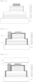
FIG. 1 is a view illustrating an example of a schematic view of a temporarily bonded wafer according to the present invention. -
FIG. 2 is a view illustrating a schematic view in which an epitaxial substrate is manufactured by growing an epitaxial functional layer on a GaAs starting substrate in the first embodiment of a method for manufacturing a temporarily bonded wafer according to the present invention. -
FIG. 3 is a view illustrating a schematic view in which a first electrode is formed on a GaP window layer in the first embodiment. -
FIG. 4 is a view illustrating a schematic view in which an AlGaInP first cladding layer is exposed by dry etching in the first embodiment. -
FIG. 5 is a view illustrating a schematic view in which a second electrode is formed on an AlGaInP first cladding layer in the first embodiment. -
FIG. 6 is a view illustrating a schematic view in which the surface of an epitaxial functional layer, where an electrode is formed, is temporarily bonded to a support substrate via BCB resin, thereby manufacturing a temporarily bonded wafer in the first embodiment. -
FIG. 7 is a view illustrating a schematic view in which a GaAs starting substrate is removed from a manufactured temporarily bonded wafer in the first embodiment. -
FIG. 8 is a view illustrating a schematic view in which a temporarily bonded wafer having a GaAs starting substrate removed adheres to a silicon wafer via silicone; then, the support substrate is delaminated in the first embodiment. -
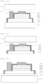
FIG. 9 is a view illustrating a schematic view in which an epitaxial functional layer is grown on a sapphire starting substrate to manufacture an epitaxial substrate in the second embodiment of a method for manufacturing a temporarily bonded wafer according to the present invention. -
FIG. 10 is a view illustrating a schematic view in which a first electrode is formed on a GaN contact layer in the second embodiment. -
FIG. 11 is a view illustrating a schematic view in which a GaN first cladding layer is exposed by dry etching in the second embodiment. -
FIG. 12 is a view illustrating a schematic view in which a second electrode is formed on a GaN first cladding layer in the second embodiment. -
FIG. 13 is a view illustrating a schematic view in which the surface of an epitaxial functional layer, where an electrode is formed, is temporarily bonded to a support substrate via BCB resin, thereby manufacturing a temporarily bonded wafer in the second embodiment. -
FIG. 14 is a view illustrating a schematic view in which a sapphire starting substrate is removed from a manufactured temporarily bonded wafer in the second embodiment. -
FIG. 15 is a view illustrating a schematic view in which a temporarily bonded wafer having a sapphire starting substrate removed adheres to a silicon wafer via silicone; then, a support substrate is delaminated in the second embodiment. - As described above, temporary bonding of a support substrate and then forming an electrode cause a problem of delamination due to heat treatment for the formation of ohmic contact. In particular, when a heterostructure is formed by combining a material system with a large lattice mismatch and a material with a large difference in coefficient of thermal expansion, the delamination rate tends to be enlarged due to a bimetallic effect at heat treatment.
- To solve the above problem, the present inventors have earnestly studied and found out that by temporarily bonding the surface of an epitaxial functional layer having two or more electrodes of different polarities to a support substrate with a thermosetting bonding material in an uncured state, a temporarily bonded area has no delamination due to heat treatment during electrode formation, and since the thermosetting bonding material is bonded in an uncured state, the temporarily bonded support substrate can be removed very easily. Based on this finding, the present invention has been completed.
- That is, the present invention is a temporarily bonded wafer in which the epitaxial functional layer having two or more electrodes with different polarities on one surface and a support substrate are temporarily bonded, wherein the surface having the electrodes of the epitaxial functional layer and the support substrate are temporarily bonded via an uncured thermosetting bonding material.
- Hereinafter, the present invention will be described in detail. However, the present invention is not limited thereto.
-
FIG. 1 shows an example of the inventive temporarily bonded wafer. In the inventive temporarily bondedwafer 100, an epitaxial functional layer 1 has twoelectrodes 2 with different polarities on one surface, and thesurface having electrodes 2 of the epitaxial functional layer 1 and asupport substrate 3 are temporarily bonded via an uncuredthermosetting bonding material 4. - A conventional temporarily bonded wafer has a structure in which an electrode is formed on one surface of an epitaxial functional layer, and the other surface (the opposite surface to the electrode formation surface) is temporarily bonded to a support substrate. This is because in the conventional method for manufacturing the temporarily bonded wafer, firstly, the epitaxial layer of an epitaxial substrate, in which the epitaxial functional layer is formed on the starting substrate, is temporarily bonded to a support substrate, then, the starting substrate is removed, and the electrode is formed on the surface where the starting substrate is removed. In contrast, the inventive temporarily bonded wafer, unlike the conventional temporarily bonded wafer, has a structure in which the electrodes are placed between the epitaxial functional layer and the support substrate. The reason for this structure is that the wafer is manufactured by temporary bonding after the formation of the electrodes, according to the inventive method for manufacturing the temporarily bonded wafer, as described later.
- Thus, the present invention provides a method for manufacturing a temporarily bonded wafer, the method being a method for temporarily bonding an epitaxial substrate in which an epitaxial functional layer is grown on a starting substrate to a support substrate, the method comprising:
- (1) forming two or more electrodes with different polarities on one surface of the epitaxial functional layer of the epitaxial substrate; and
- (2) temporarily bonding the support substrate to the surface on which the electrodes are formed via an uncured thermosetting bonding material.
- Such a method for manufacturing the temporarily bonded wafer, unlike the conventional method in which heat treatment is performed to form an ohmic contact of electrodes (Ohmic heat treatment) to the wafer having a temporarily bonded portion, performs the electrode formation and ohmic heat treatment to the wafer before the formation of the temporarily bonded portion, then performs temporarily bonding with the support substrate. Consequently, heat treatment at a high temperature to form the electrodes does not cause delamination or thermal deformation at the temporarily bonded portion. Thus, the temporarily bonded wafer can be manufactured with an excellent yield. Furthermore, in the inventive method for manufacturing the temporarily bonded wafer, temporary bonding is performed via an uncured thermosetting bonding material. Thus, the support substrate is easily removed.
- Hereinafter, the embodiments of the present invention will be described in detail with reference to drawings. However, the present invention is not limited thereto.
- With reference to
FIG. 2 to FIG. 8 , a first embodiment of the inventive method for manufacturing a temporarily bonded wafer is described. In the first embodiment, the epitaxial functional layer contains an AlGaInP-based material. - Firstly, as illustrated in
FIG. 2 , a GaAs buffer layer 102 of the first conductivity type is laminated on a GaAs starting substrate 101 of the first conductivity type, then the following layers are grown sequentially on the substrate: a GayIn1-yP (0.4≤y≤0.6) first etching stop layer 103 of the first conductivity type having a thickness of e.g., 0.3 um; a GaAs second etching stop layer 104 of the first conductivity type having a thickness of e.g., 0.3 µm; a (AlxGa1-x)yIn1-yP (0<x≤1,0.4≤y≤0.6) first cladding layer 105 of the first conductivity type having a thickness of e.g., 1.0 um; a non-doped (AlxGa1-x)yIn1-yP (0≤x≤0.6,0.4≤y≤0.6) active layer 106; a (AlxGa1-x)yIn1-yP (0<x≤1,0.4≤y≤0.6) second cladding layer 107 of the second conductivity type having a thickness of e.g., 1.0 µm; a GayIn1-yP (0.45≤y≤1) intermediate layer 108 of the second conductivity type having a thickness of e.g., 0.1 um; a GaP window layer 109 of the second conductivity type having a thickness of e.g., 4 um; thus an epitaxial substrate having a light emitting element structure, which is a sequentially grown epitaxial functional layer, is provided. At this point, the AlGaInPfirst cladding layer 105 to the AlGaInPsecond cladding layer 107 are referred to as a double-hetero (DH) structure portion 111 (FIG. 3 ). - Then, as shown in
FIG. 3 , in a part of a region in theGaP window layer 109 of the second conductivity type, afirst electrode 110 is formed. The use of highly reflective metal is suitable for thefirst electrode 110, and the electrode can be an Au-based electrode. For example, AuBe alloy can be used as the metal in contact with theGaP window layer 109, and Au can be laminated on the alloy. Thus, thefirst electrode 110 is formed. - The metal in contact with the
GaP window layer 109 of the second conductivity type is not limited to AuBe alloys, but any metal or alloy can be selected as long as ohmic contact can be formed. In general, other than AuBe, an alloy such as AuZn is often selected. - Then, as shown in
FIG. 4 , after the formation of thefirst electrode 110, a part of a region other than thefirst electrode 110 formation region on theGaP window layer 109 of the second conductivity type is coated with a mask using a material having etching selectivity such as SiO2 or SiNx, and the exposed portion is notched by a method such as dry etching, and then the AlGaInPfirst cladding layer 105 of the first conductivity type is exposed. - Then, as shown in
FIG. 5 , theGaP window layer 109 of the second conductivity type, the side surface of the notched portion, and the AlGaInPfirst cladding layer 105 of the first conductivity type are coated with SiO2 or SiNx as a PSV (passivation)film 113, then, thefirst electrode 110 portion and a part of the AlGaInPfirst cladding layer 105 of the first conductivity type are exposed by a photolithography method. Then, thesecond electrode 112 is formed on the exposed portion on the AlGaInPfirst cladding layer 105 of the first conductivity type. - The use of a highly reflective metal is suitable for the
second electrode 112, and the electrode can be an Au-based electrode. For example, an AuSi alloy can be used as the metal to come in contact with the AlGaInPfirst cladding layer 105 of the first conductivity type, and Au can be laminated on the metal. Thus, thesecond electrode 112 is formed. - Furthermore, the metal in contact with the
AlGaInP cladding layer 105 of the first conductivity type is not limited to AuSi alloys, but any metal or alloy can be selected as long as ohmic contact can be formed. In general, other than AuSi, alloys such as AuGe are often selected. - In addition, the
PSV film 113 is not necessarily formed before the formation of thesecond electrode 112, and thePSV film 113 may be formed after the formation of thesecond electrode 112. Furthermore, the same effect can be obtained without the formation of thePSV film 113. - After the formation of the first and
second electrodes - Then, as shown in
FIG. 6 , after the formation of ohmic contact, the electrode formation side is spin-coated with aBCB resin 114, then faced each other with thesupport substrate 115 selected from such as silicon, and then pressurized in a vacuum atmosphere and retained at 150°C for 15 minutes, and then temporarily bonded to thesupport substrate 115. Since theBCB resin 114 is cured by retaining the temperature condition above 150°C, theBCB resin 114 is prevented from being cured by retaining the temperature at 150°C or less. Theuncured BCB resin 114 can improve the delamination property of thesupport substrate 115 from the epitaxial substrate. - In addition, the thermosetting bonding material is not limited to benzocyclobutene (BCB) resin; for example, the material can be polyimide (PI) resin, fluororesin, and epoxy resin.
- Moreover, the
support substrate 115 is not limited to silicon, but any material with excellent surface flatness can be selected, such as sapphire, GaP, GaAs, InP, quartz, glass, LiTaO3, LiNbO3, rock crystal, and SiC. - Then, as shown in
FIG. 7 , after the temporarily bonding to thesupport substrate 115, the starting substrate is removed by a selective etching method. TheGaAs starting substrate 101 is removed by ammonia hydrogen peroxide water. The GaInP firstetching stop layer 103 is removed by diluted hydrochloric acid or hydrochloric acid-based etchant, and lastly, the GaAs secondetching stop layer 104 is removed by sulfuric acid-hydrogen peroxide mixture, and then the AlGaInPfirst cladding layer 105 of the first conductivity type is exposed. Consequently, the temporarily bonded wafer can be manufactured. - Lastly, as shown in
FIG. 8 , after exposing the AlGaInPfirst cladding layer 105 of the first conductivity type on the temporarily bonded wafer, this layer is adhered to asilicon wafer 117 coated withsilicone 116, thenBCB resin 114 in a softened state is dissolved by BCB solvent, thus delaminating thesupport substrate 115 and then individually divided chips are produced. - Using
FIG. 9 to FIG. 15 , a second embodiment of the inventive method for manufacturing a temporarily bonded wafer is described. In the second embodiment, the epitaxial functional layer includes InGaN-based material. - Firstly, as shown in
FIG. 9 , aGaN buffer layer 202 of the first conductivity type is laminated on asapphire starting substrate 201, and then the following layers are grown sequentially on the substrate: a GaNfirst cladding layer 203 of the first conductivity type having a thickness, e.g., 1.0 µm; non-doped InzGa1-zN (0<z≤0.4)active layer 204; an AlvGa1-vN (0≤v≤0.4) (GaN)second cladding layer 205 of the second conductivity type having a thickness of e.g., 1.0 um; aGaN contact layer 206 of the second conductivity type having a thickness of e.g., 0.1 um; thus an epitaxial substrate having a light emitting element structure, which is a sequentially grown epitaxial functional layer, is provided. At this point, the GaNfirst cladding layer 203 to the AlGaNsecond cladding layer 205 are referred to as a double-hetero (DH) structure 208 (FIG. 10 ). - Then, as shown in
FIG. 10 , in a part of a region in theGaN contact layer 206 of the second conductivity type, afirst electrode 207 is formed. The use of a highly reflective metal for thefirst electrode 207 is suitable, and the electrode can be an Ag-based electrode. Ag can be used as the metal in contact with theGaN contact layer 206, and Pd can be laminated on the metal. Thus, thefirst electrode 207 is formed. - Moreover, the metal in contact with the
GaN contact layer 206 of the second conductivity type is not limited to an Ag-based metal, but any metal or alloy can be selected as long as ohmic contact can be formed. Generally, metals other than Ag, such as Au, and Ti, are often selected. - Then, as shown in
FIG. 11 , after the formation of thefirst electrode 207, a part of a region other than thefirst electrode 207 formation region on theGaN contact layer 206 of the second conductivity type is coated with a mask using a material having etching selectivity such as SiO2 or SiNx, and the exposed portion is notched by a method such as dry etching. Then, the GaNfirst cladding layer 203 of the first conductivity type is exposed. - Then, as shown in
FIG. 12 , theGaN contact layer 206, the side surface of the notched portion, the GaNfirst cladding layer 203 are coated with SiO2 or SiNx as aPSV film 210, then, thefirst electrode 207 portion and a part of the GaNfirst cladding layer 203 are exposed by a photolithography method. Then, thesecond electrode 209 is formed on the exposed portion of the GaNfirst cladding layer 203. - Moreover, the use of a highly reflective metal is suitable for the
second electrode 209, and the electrode can be an Al-based electrode. For example, an Al metal can be used as the metal to come in contact with the GaNfirst cladding layer 203 of the first conductivity type, and Au can be laminated on the metal. Thus, thesecond electrode 209 is formed. - Furthermore, the metal in contact with the GaN
first cladding layer 203 of the first conductivity type is not limited to Al metal, but any metal or alloy can be selected as long as ohmic contact can be formed. In general, other than Al, metals such as Ti or Au are often selected. - In addition, the
PSV film 210 is not necessarily formed before the formation of thesecond electrode 209, and thePSV film 210 may be formed after the formation of thesecond electrode 209. Furthermore, the same effect can be obtained without the formation of thePSV film 210. - After the formation of the first and
second electrodes - Then, as shown in
FIG. 13 , after the formation of ohmic contact, the electrode formation side is spin-coated withBCB resin 211, faced each other with thesupport substrate 212 selected from such as silicon, and then pressurized in a vacuum atmosphere and retained approximately at 150°C for 15 minutes, and then temporarily bonded to thesupport substrate 212. Since theBCB resin 211 is cured by retaining the temperature condition above 150°C, theBCB resin 211 is prevented from being cured by retaining the temperature at 150°C or less. Theuncured BCB resin 211 can improve the delamination property of thesupport substrate 212 from the epitaxial substrate. - In addition, the thermosetting bonding material is not limited to benzocyclobutene (BCB) resin; for example, the material can be polyimide (PI) resin, fluororesin, and epoxy resin.
- Moreover, the
support substrate 212 is not limited to silicon, but any material with excellent surface flatness can be selected. Such as sapphire, GaP, GaAs, InP, quartz, glass, LiTaO3, LiNbO3, rock crystal, and SiC can be selected. - Then, as shown in
FIG. 14 , after temporary bonding, theGaN buffer layer 202 is irradiated by a laser from the starting substrate side for ablation, thus, thesapphire starting substrate 201 is removed, and the GaNfirst cladding layer 203 of the first conductivity type is exposed. Consequently, the temporarily bonded wafer can be manufactured. - Lastly, as shown in
FIG. 15 , after the GaNfirst cladding layer 203 of the first conductivity type is exposed, this layer adheres with asilicon wafer 214 on whichsilicone 213 is coated, thenBCB resin 211 in softened state is dissolved by BCB solvent, thus delaminating thesupport substrate 212, and then individually divided chips are produced. - Hereinafter, the present invention will be specifically described with reference to Examples and Comparative Example. However, the present invention is not limited thereto.
- A GaAs buffer layer of the first conductivity type was laminated on a GaAs starting substrate of the first conductivity type, and then the following layers were grown sequentially on the substrate: a GayIn1-yP (0.4≤y≤0.6) first etching stop layer of the first conductivity type having a thickness of 0.3 um; a GaAs second etching stop layer of the first conductivity type having 0.3 µm; a (AlxGa1-x)yIn1-yP (0<x≤1,0.4≤y≤0.6) first cladding layer of the first conductivity type having a thickness of 1.0 um; a non-doped (AlxGa1-x)yIn1-yP (0≤x≤0.6,0.4≤y≤0.6) active layer; a (AlxGa1-x)yIn1-yP (0<x≤1,0.4≤y≤0.6) second cladding layer of the second conductivity type having a thickness of 1.0 µm; a GayIn1-yP (0.45≤y≤1) intermediate layer of the second conductivity type having a thickness of 0.1µm; and a GaP window layer of the second conductivity type having a thickness of 4 um; thus an epitaxial substrate having a light emitting element structure, which was a sequentially grown epitaxial functional layer, was provided (see
FIG. 2 ). - Then, a first electrode was formed in a part of a region on the GaP window layer of the second conductivity type. The use of a highly reflective metal was suitable for the first electrode; thus, an Au-based electrode was used. In this technique, AuBe alloy was used for the metal in contact with the GaP window layer, and Au was laminated on the alloy. Thus, the first electrode was formed (see
FIG. 3 ). - After the formation of the first electrode, a part of a region of the GaP window layer of the second conductivity type, other than the area where the first electrode was formed, was coated with SiO2, and the exposed portion was notched by dry etching, thus, the AlGaInP first cladding layer of the first conductivity type was exposed (see
FIG.4 ). - The GaP window layer of the second conductivity type, the side surface of the notched portion, and the AlGaInP first cladding layer of the first conductivity type were coated with SiO2 as a PSV film, then the first electrode portion and a part of the AlGaInP first cladding layer of the first conductivity type were exposed by a photolithography method. Then, the second electrode was formed on the exposed portion of the AlGaInP first cladding layer of the first conductivity type. At this point, the second electrode was formed using AuSi alloy as the metal in contact with the AlGaInP first cladding layer of the first conductivity type and laminating Au on the alloy (see
FIG. 5 ). - After the formation of the first and second electrodes, to obtain ohmic contact, RTA heat treatment was performed at 400°C for 5 minutes.
- After the formation of ohmic contact, the electrode formation side was spin-coated with BCB resin, then faced each other with a support substrate made of silicon, and then pressurized in a vacuum atmosphere and retained approximately at 150°C for 15 minutes, and then temporarily bonded to the support substrate (see
FIG. 6 ) . - After the temporary bonding to the support substrate, the GaAs starting substrate was removed by ammonia hydrogen peroxide water, the GaInP first etching stop layer was removed by diluted hydrochloric acid or hydrochloric acid-based etchant, and lastly, the GaAs second etching stop layer was removed by sulfuric acid-hydrogen peroxide mixture. Thus, the AlGaInP first cladding layer of the first conductivity type was exposed (see
FIG. 7 ) - After exposing the AlGaInP first cladding layer of the first conductivity type, the layer was adhered to a silicon wafer coated with silicone, then the BCB resin in a softened state was dissolved by BCB solvent, thus delaminating the support substrate, and then individually divided chips were produced (see
FIG. 8 ). - A GaN buffer layer of the first conductivity type was laminated on a sapphire starting substrate, and then the following layers were grown sequentially on the substrate: a GaN first cladding layer of the first conductivity type having a thickness of 1.0 µm; non-doped InzGa1-zN (0<z≤0.4) active layer; an AlvGa1-vN (0≤v≤0.4) (GaN) second cladding layer of the second conductivity type having a thickness of 1.0 um; a GaN contact layer of the second conductivity type having a thickness of 0.1 µm; thus, an epitaxial substrate having a light emitting element structure, which is a sequentially grown epitaxial functional layer, is provided (see
FIG. 9 ). - Then, in a part of a region of the GaN contact layer of the second conductive type, using Ag as the metal in contact with the GaN contact layer and laminating Pd thereon, the first electrode was formed (see
FIG. 10 ). - After the formation of the first electrode, a part of a region of the GaN contact layer of the second conductivity type, other than the area where the first electrode was formed, was coated with SiO2, and the exposed portion was notched by dry etching, thus, the GaN first cladding layer of the first conductivity type was exposed (see
FIG.11 ). - The GaN contact layer, the side surface of the notched portion, and the GaN first cladding layer were coated with SiO2 as a PSV film, then the first electrode portion and a part of the GaN first cladding layer were exposed by a photolithography method. Then, the second electrode was formed on the exposed portion of the GaN first cladding layer by using an Al metal as the metal in contact with the GaN first cladding layer of the first conductivity type and laminating Au on the Al metal (see
FIG. 12 ). - After the formation of the first and second electrodes, to obtain ohmic contact, RTA heat treatment was performed at 700°C for 5 minutes.
- After the formation of ohmic contact, the electrode formation side was spin-coated with BCB resin, faced each other with the support substrate made of silicon, and then pressurized in a vacuum atmosphere and retained approximately at 150°C for 15 minutes, and then temporarily bonded to the support substrate (see
FIG. 13 ) . - After temporary bonding, the GaN buffer layer was irradiated by a laser from the starting substrate side for ablation, thus, the starting substrate was removed, and the GaN first cladding layer of the first conductivity type was exposed (see
FIG. 14 ). - After the GaN cladding layer of the first conductivity type was exposed, this layer adhered with a silicon wafer on which silicone was coated, then the BCB resin in a softened state was dissolved by BCB solvent, thus delaminating the support substrate and then individually divided chips were produced (see.
FIG.15 ). - After lamination of a GaAs buffer layer of the first conductivity type on a GaAs starting substrate of the first conductivity type, the following layers were grown sequentially: a GayIn1-yP (0.4≤y≤0.6) first etching stop layer of the first conductivity type having a thickness of 0.3 um; a GaAs second etching stop layer of the first conductivity type having a thickness of 0.3 µm; a (AlxGa1-x)yIn1-yP (0<x≤1,0.4≤y≤0.6) first cladding layer of the first conductivity type having a thickness of 1.0 um; a non-doped (AlxGa1-x)yIn1-yP (0≤x≤0.6,0.4≤y≤0.6) active layer; a (AlxGa1-x)yIn1-yP (0<x≤1,0.4≤y≤0.6) second cladding layer of the second conductivity type having a thickness of 1.0 µm; a GayIn1-yP (0.45≤y≤1) intermediate layer of the second conductivity type having a thickness of 0.1 um; a GaP window layer of the second conductivity type having a thickness of 4 um; thus an epitaxial substrate having a light emitting element structure, which was a sequentially grown epitaxial functional layer, was provided.
- The epitaxial substrate was spin-coated with 1.0 um of BCB resin, faced and superimposed with a sapphire wafer, and thermocompression-bonded. Thereby, an epitaxial bonded substrate in which the epitaxial substrate and the sapphire wafer was bonded with each other via BCB was manufactured. During the bonding, the curing process was performed by retaining at 250°C for 1 hour.
- The GaAs starting substrate was removed by ammonia hydrogen peroxide water and the GaInP first etching stop layer was exposed. By switching the etchant to hydrochloric acid-based, the GaInP first etching stop layer was removed, and the GaAs second etching stop layer was exposed. By switching the etchant to sulfuric acid-hydrogen peroxide mixture-based, the GaAs second etching stop layer was removed, and the first cladding layer was exposed. By performing the processes above, the epitaxial bonded substrate having only a double-hetero layer and a window layer was manufactured.
- After removing the starting substrate, AuBe-based was used as the metal in contact with the starting substrate-removal surface (first cladding layer), and Au was laminated on the top to form the first electrode.
- After forming the first electrode, a part of a region of the first cladding layer, other than the area where the first electrode was formed, was notched by dry-etching, and the second cladding layer was exposed on the notched portion.
- The AlGaInP first cladding layer, the side surface of the notched portion, and the AlGaInP second cladding layer were coated with a passivation (PSV) film; then, the first electrode portion and a part of the AlGaInP second cladding layer were exposed by a photolithography method. Then, the second electrode made of Au was formed on the exposed portion of the second cladding layer.
- After forming the first and second electrodes, RTA heat treatment was performed at 400°C for 5 minutes to obtain ohmic contact.
- After adhesion with a silicone-coated wafer, a laser was irradiated from the support substrate side for ablation, and then the support substrate and the element were separated.
- Temporarily bonded wafers manufactured in Examples 1 and 2, and Comparative Example were compared in light of area yield, doping level, area yield when P-CVD is adopted, and leakage failure rate as follows.
- Table 1 shows a comparison of yield (ratio of adhesive area). In Example 1 and Example 2, since the electrode formation process and the element separation process were completed before temporary bonding, the temporarily bonded area was not delaminated or deformed by an ohmic heat treatment, and the process was performed to a wafer with excellent flatness and warpage. Consequently, the yield of the electrode formation process and the element separation process was maintained at a comparable level with the non-bonded wafers. On the other hand, in Comparative Example, a wafer having a temporarily bonded portion was applied to high-temperature RTA heat treatment, and the temporarily bonded portion was delaminated or deformed. Thus, a sufficient yield was not obtained.
[Table 1] Example 1 Example 2 Comparative Example Effective Area 97%∼99% 96%∼99% 10∼47% - Even with applying curing treatment, a BCB film loses bonding strength when the film exceeds the softening point. Therefore, a high temperature processing should not be performed. To form ohmic contact, it is required to employ one of the following methods: the process is performed at a temperature higher than the softening point of BCB; and the metal contact layer is highly doped to avoid high-temperature treatment. However, heat treatment above the BCB softening point tends to induce deformation of the BCB bonded layer, leading to a decrease in an element yield. On the other hand, a highly doped contact layer easily induces an element degradation during energization through electromigration effect during energization, leading to performance degradation. When the process for electrode formation and element separation is performed in a wafer state where a BCB bonded wafer has not been formed, it is possible to effectively avoid the thermal restriction and the restrictions in designing an epitaxial substrate. Therefore, it is possible to increase the degree of freedom in design and avoid quality degradation of the element due to the process restriction.
- Doping levels required for the first and the second electrode contact layers in Example 1, Example 2, and Comparative Example are shown in Table 2. In Examples, high-temperature heat treatment during electrode formation is possible. Consequently, ohmic contact can be obtained at the doping level of 10 to the power of seventeen. On the other hand, in Comparative Example, an ohmic heat treatment for electrode formation is performed on a wafer including a BCB temporarily bonded portion; thus, when a high-temperature treatment is performed, the temporarily bonded potion is delaminated. Consequently, in Comparative Example, heat treatment at a low temperature is needed to maintain a high yield. Thus, the doping level of 10 to the power of eighteen level is needed.
- When a cladding layer having a doping level of 10 to the power of eighteen is formed, a defect tends to occur in an active layer due to electromigration during energization; it is highly possible that the element is degraded by energizing. A light-emitting element doped at 10 to the power of eighteen level shows a satisfied quality only in the initial characteristic but cannot show a satisfied quality in the transient characteristic. In Examples, since an epitaxial layer having a one-digit lower doping level can be introduced, the problem produced in Comparative Example, in which an unsatisfactory transient characteristic is produced, can be avoided.
[Table 2] Example 1 Example 2 Comparative Example First electrode contact layer 1∼5E+17[/cm3] 1∼3E+17[/cm3] 1∼2E+18[/cm3] Second electrode contact layer 1∼5E+17[/cm3] 1∼5E+17[/cm3] 1∼2E+18[/cm3] - To form SiO2 as a PSV film, a film-forming method such as P-CVD is needed, and a heat environment of 400°C or more is needed due to a factor of the material reaction system. When the film-forming is performed by P-CVD after BCB bonding (Comparative Example), the film-forming needs to be performed under the condition of the BCB softening point. Thus, deformation of the BCB film is likely to occur during film-forming. Deformation of the BCB film is manifested as an uplift (delamination) phenomenon of the epitaxial layer, eventually leading to delamination of the uplift portions, thereby decreasing the yield.
- Table 3 shows the yield when the P-CVD process is introduced (adhesive area ratio). As shown in Table 3, high yields were obtained in Examples; by contrast, in Comparative Example, in which the PSV film formation process was performed after the temporary bonding, the yield was decreased due to the occurrence of the delamination at the bonding portion during PSV film-forming process.
[Table 3] Example 1 Example 2 Comparative Example Effective Area 97%∼100% 95%∼100% 16∼68% - If the PSV film is only a hard mask, a film-forming method other than a P-CVD method, e.g., a physical film-forming method, can be selected. However, in the PSV film formation, the physical film-forming method has a poor coverage rate at the side surface, thus having a problem that cannot suppress a leakage occurring at the side surface.
- Therefore, as shown in Table 4, Comparative Example that cannot adopt the most suitable P-CVD method for the PSV film-forming had a higher leakage failure rate compared with Example 1 and Example 2, which were able to adopt the P-CVD method.
[Table 4] Example 1 Example 2 Comparative Example Leakage failure rate 0.01%∼3.75% 0.01%∼4.11% 58∼100% - It should be noted that the present invention is not limited to the above-described embodiments. The embodiments are just examples, and any examples that have substantially the same feature and demonstrate the same functions and effects as those in the technical concept disclosed in claims of the present invention are included in the technical scope of the present invention.
Claims (12)
- A temporarily bonded wafer in which an epitaxial functional layer having two or more electrodes with different polarities on one surface and a support substrate are temporarily bonded, wherein
the surface having the electrodes of the epitaxial functional layer and the support substrate are temporarily bonded via an uncured thermosetting bonding material. - The temporarily bonded wafer according to claim 1, wherein
the epitaxial functional layer is a light emitting element. - The temporarily bonded wafer according to claim 1 or 2, wherein
the epitaxial functional layer contains an AlGaInP-based or InGaN-based material. - The temporarily bonded wafer according to any one of claims 1 to 3, wherein
the thermosetting bonding material is any of benzocyclobutene (BCB) resin, polyimide (PI) resin, fluororesin, and epoxy resin. - The temporarily bonded wafer according to any one of claims 1 to 4, wherein
the support substrate is comprised of any of the materials: silicon, sapphire, GaP, GaAs, InP, SiC, quartz, glass, LiTaO3, and LiNbO3. - The temporarily bonded wafer according to any one of claims 1 to 5, wherein
the wafer does not have a starting substrate on a surface of the epitaxial functional layer opposite to the surface having the electrodes. - A method for manufacturing a temporarily bonded wafer, the method being a method for temporarily bonding an epitaxial substrate in which an epitaxial functional layer is grown on a starting substrate to a support substrate, the method comprising:(1) forming two or more electrodes with different polarities on one surface of the epitaxial functional layer of the epitaxial substrate; and(2) temporarily bonding the support substrate to the surface on which the electrodes are formed via an uncured thermosetting bonding material.
- The method for manufacturing a temporarily bonded wafer according to claim 7, wherein
the epitaxial functional layer is a light emitting element. - The method for manufacturing a temporarily bonded wafer according to claim 7 or 8, wherein
the epitaxial functional layer contains an AlGaInP-based or InGaN-based material. - The method for manufacturing a temporarily bonded wafer according to any one of claims 7 to 9, wherein
the thermosetting bonding material is any of benzocyclobutene (BCB) resin, polyimide (PI) resin, fluororesin, and epoxy resin. - The method for manufacturing a temporarily bonded wafer according to any one of claims 7 to 10, wherein
the support substrate is comprised of any of the materials: silicon, sapphire, GaP, GaAs, InP, SiC, quartz, glass, LiTaO3, and LiNbO3. - The method for manufacturing a temporarily bonded wafer according to any one of claims 7 to 11, the method further comprising: after (2),
(3) removing the starting substrate from the epitaxial substrate.
Applications Claiming Priority (2)
| Application Number | Priority Date | Filing Date | Title |
|---|---|---|---|
| JP2021132721 | 2021-08-17 | ||
| PCT/JP2022/029483 WO2023021972A1 (en) | 2021-08-17 | 2022-08-01 | Provisionally bonded wafer and method for producing same |
Publications (2)
| Publication Number | Publication Date |
|---|---|
| EP4391018A1 true EP4391018A1 (en) | 2024-06-26 |
| EP4391018A4 EP4391018A4 (en) | 2025-09-10 |
Family
ID=85240597
Family Applications (1)
| Application Number | Title | Priority Date | Filing Date |
|---|---|---|---|
| EP22858293.8A Pending EP4391018A4 (en) | 2021-08-17 | 2022-08-01 | Provisionally bonded wafer and method for producing the same |
Country Status (6)
| Country | Link |
|---|---|
| US (1) | US20240347668A1 (en) |
| EP (1) | EP4391018A4 (en) |
| JP (1) | JP7666608B2 (en) |
| CN (1) | CN117813674A (en) |
| TW (1) | TW202316494A (en) |
| WO (1) | WO2023021972A1 (en) |
Family Cites Families (6)
| Publication number | Priority date | Publication date | Assignee | Title |
|---|---|---|---|---|
| TW544958B (en) | 2002-07-15 | 2003-08-01 | Epistar Corp | Light emitting diode with an adhesive layer and its manufacturing method |
| JP4715370B2 (en) | 2005-07-29 | 2011-07-06 | 信越半導体株式会社 | Light emitting device and manufacturing method thereof |
| JP2008187160A (en) | 2007-01-05 | 2008-08-14 | Rohm Co Ltd | Semiconductor light emitting device and method for manufacturing semiconductor light emitting device |
| GB2539684B (en) * | 2015-06-24 | 2018-04-04 | Dst Innovations Ltd | Method of surface-mounting components |
| KR102558905B1 (en) * | 2017-07-14 | 2023-07-21 | 신에쓰 가가꾸 고교 가부시끼가이샤 | High thermal conductivity device substrate and manufacturing method thereof |
| JP2021027301A (en) * | 2019-08-08 | 2021-02-22 | 信越半導体株式会社 | Temporary bonding method of semiconductor substrate |
-
2022
- 2022-08-01 JP JP2023542313A patent/JP7666608B2/en active Active
- 2022-08-01 CN CN202280055853.8A patent/CN117813674A/en active Pending
- 2022-08-01 US US18/683,042 patent/US20240347668A1/en active Pending
- 2022-08-01 EP EP22858293.8A patent/EP4391018A4/en active Pending
- 2022-08-01 WO PCT/JP2022/029483 patent/WO2023021972A1/en not_active Ceased
- 2022-08-03 TW TW111129072A patent/TW202316494A/en unknown
Also Published As
| Publication number | Publication date |
|---|---|
| WO2023021972A1 (en) | 2023-02-23 |
| JP7666608B2 (en) | 2025-04-22 |
| TW202316494A (en) | 2023-04-16 |
| US20240347668A1 (en) | 2024-10-17 |
| JPWO2023021972A1 (en) | 2023-02-23 |
| EP4391018A4 (en) | 2025-09-10 |
| CN117813674A (en) | 2024-04-02 |
Similar Documents
| Publication | Publication Date | Title |
|---|---|---|
| CN101901858B (en) | Vertical structure semiconductor devices | |
| WO2012147436A9 (en) | MANUFACTURING METHOD FOR GaN SEMICONDUCTOR DEVICE | |
| US9070819B2 (en) | Method for manufacturing thin film compound solar cell | |
| TWI894292B (en) | Junction type semiconductor element and method for manufacturing the same | |
| KR20240150451A (en) | Wide band gap device integrated circuit architecture on engineered substrate | |
| JP4638000B2 (en) | Manufacturing method of semiconductor substrate | |
| US20260107606A1 (en) | Chip on carrier and method of manufacturing the same | |
| JP4110524B2 (en) | Light emitting device and method for manufacturing light emitting device | |
| JP4062111B2 (en) | Method for manufacturing light emitting device | |
| US20240347668A1 (en) | Temporarily bonded wafer and method for manufacturing the wafer | |
| JPH0831791A (en) | Method for manufacturing semiconductor layer | |
| JP2014175335A (en) | Composite multilayer substrate and group iii nitride semiconductor device manufacturing method | |
| JP5196288B2 (en) | Light emitting device manufacturing method and light emitting device | |
| JP4120796B2 (en) | Light emitting device and method for manufacturing light emitting device | |
| JP2005123530A (en) | Method for manufacturing light emitting device | |
| KR101574267B1 (en) | Supporting substrate for light eimming device and method of manufacturing a light emitting device using the same | |
| KR102711294B1 (en) | Method for manufacturing electronic devices | |
| US20100041209A1 (en) | Method for manufacturing semiconductor device | |
| KR102756022B1 (en) | Chip on carrier and method of manufacturing the same | |
| JP2026056457A (en) | Bonded wafer and method for manufacturing the same | |
| JP7619464B2 (en) | Manufacturing method of bonded wafer | |
| JP2005197286A (en) | Handling method of semiconductor thin film and manufacturing method of light-emitting element | |
| CN107851699A (en) | The installation method of luminescence component | |
| WO2022249675A1 (en) | Method for manufacturing compound semiconductor junction substrate, and compound semiconductor junction substrate | |
| KR20160034861A (en) | Supporting substrate for light eimming device and method of manufacturing a light emitting device using the same |
Legal Events
| Date | Code | Title | Description |
|---|---|---|---|
| STAA | Information on the status of an ep patent application or granted ep patent |
Free format text: STATUS: THE INTERNATIONAL PUBLICATION HAS BEEN MADE |
|
| PUAI | Public reference made under article 153(3) epc to a published international application that has entered the european phase |
Free format text: ORIGINAL CODE: 0009012 |
|
| STAA | Information on the status of an ep patent application or granted ep patent |
Free format text: STATUS: REQUEST FOR EXAMINATION WAS MADE |
|
| 17P | Request for examination filed |
Effective date: 20240208 |
|
| AK | Designated contracting states |
Kind code of ref document: A1 Designated state(s): AL AT BE BG CH CY CZ DE DK EE ES FI FR GB GR HR HU IE IS IT LI LT LU LV MC MK MT NL NO PL PT RO RS SE SI SK SM TR |
|
| DAV | Request for validation of the european patent (deleted) | ||
| DAX | Request for extension of the european patent (deleted) | ||
| A4 | Supplementary search report drawn up and despatched |
Effective date: 20250811 |
|
| RIC1 | Information provided on ipc code assigned before grant |
Ipc: H01L 21/02 20060101AFI20250805BHEP Ipc: H10H 20/01 20250101ALI20250805BHEP Ipc: H10H 29/01 20250101ALI20250805BHEP Ipc: H10H 29/03 20250101ALI20250805BHEP |