EP4388579B1 - Systems and methods for processing semiconductor wafers using front-end processed wafer geometry metrics - Google Patents
Systems and methods for processing semiconductor wafers using front-end processed wafer geometry metrics Download PDFInfo
- Publication number
- EP4388579B1 EP4388579B1 EP22764521.5A EP22764521A EP4388579B1 EP 4388579 B1 EP4388579 B1 EP 4388579B1 EP 22764521 A EP22764521 A EP 22764521A EP 4388579 B1 EP4388579 B1 EP 4388579B1
- Authority
- EP
- European Patent Office
- Prior art keywords
- wafer
- profile
- gapi
- scan line
- value
- Prior art date
- Legal status (The legal status is an assumption and is not a legal conclusion. Google has not performed a legal analysis and makes no representation as to the accuracy of the status listed.)
- Active
Links
Images


Classifications
-
- B—PERFORMING OPERATIONS; TRANSPORTING
- B24—GRINDING; POLISHING
- B24B—MACHINES, DEVICES, OR PROCESSES FOR GRINDING OR POLISHING; DRESSING OR CONDITIONING OF ABRADING SURFACES; FEEDING OF GRINDING, POLISHING, OR LAPPING AGENTS
- B24B37/00—Lapping machines or devices; Accessories
- B24B37/005—Control means for lapping machines or devices
-
- B—PERFORMING OPERATIONS; TRANSPORTING
- B24—GRINDING; POLISHING
- B24B—MACHINES, DEVICES, OR PROCESSES FOR GRINDING OR POLISHING; DRESSING OR CONDITIONING OF ABRADING SURFACES; FEEDING OF GRINDING, POLISHING, OR LAPPING AGENTS
- B24B49/00—Measuring or gauging equipment for controlling the feed movement of the grinding tool or work; Arrangements of indicating or measuring equipment, e.g. for indicating the start of the grinding operation
- B24B49/02—Measuring or gauging equipment for controlling the feed movement of the grinding tool or work; Arrangements of indicating or measuring equipment, e.g. for indicating the start of the grinding operation according to the instantaneous size and required size of the workpiece acted upon, the measuring or gauging being continuous or intermittent
- B24B49/03—Measuring or gauging equipment for controlling the feed movement of the grinding tool or work; Arrangements of indicating or measuring equipment, e.g. for indicating the start of the grinding operation according to the instantaneous size and required size of the workpiece acted upon, the measuring or gauging being continuous or intermittent according to the final size of the previously ground workpiece
-
- B—PERFORMING OPERATIONS; TRANSPORTING
- B24—GRINDING; POLISHING
- B24B—MACHINES, DEVICES, OR PROCESSES FOR GRINDING OR POLISHING; DRESSING OR CONDITIONING OF ABRADING SURFACES; FEEDING OF GRINDING, POLISHING, OR LAPPING AGENTS
- B24B9/00—Machines or devices designed for grinding edges or bevels on work or for removing burrs; Accessories therefor
- B24B9/02—Machines or devices designed for grinding edges or bevels on work or for removing burrs; Accessories therefor characterised by a special design with respect to properties of materials specific to articles to be ground
- B24B9/06—Machines or devices designed for grinding edges or bevels on work or for removing burrs; Accessories therefor characterised by a special design with respect to properties of materials specific to articles to be ground of non-metallic inorganic material, e.g. stone, ceramics, porcelain
- B24B9/065—Machines or devices designed for grinding edges or bevels on work or for removing burrs; Accessories therefor characterised by a special design with respect to properties of materials specific to articles to be ground of non-metallic inorganic material, e.g. stone, ceramics, porcelain of thin, brittle parts, e.g. semiconductors, wafers
-
- G—PHYSICS
- G01—MEASURING; TESTING
- G01B—MEASURING LENGTH, THICKNESS OR SIMILAR LINEAR DIMENSIONS; MEASURING ANGLES; MEASURING AREAS; MEASURING IRREGULARITIES OF SURFACES OR CONTOURS
- G01B11/00—Measuring arrangements characterised by the use of optical techniques
- G01B11/02—Measuring arrangements characterised by the use of optical techniques for measuring length, width or thickness
- G01B11/06—Measuring arrangements characterised by the use of optical techniques for measuring length, width or thickness for measuring thickness ; e.g. of sheet material
- G01B11/0608—Height gauges
-
- G—PHYSICS
- G01—MEASURING; TESTING
- G01B—MEASURING LENGTH, THICKNESS OR SIMILAR LINEAR DIMENSIONS; MEASURING ANGLES; MEASURING AREAS; MEASURING IRREGULARITIES OF SURFACES OR CONTOURS
- G01B11/00—Measuring arrangements characterised by the use of optical techniques
- G01B11/24—Measuring arrangements characterised by the use of optical techniques for measuring contours or curvatures
- G01B11/2441—Measuring arrangements characterised by the use of optical techniques for measuring contours or curvatures using interferometry
-
- G—PHYSICS
- G01—MEASURING; TESTING
- G01B—MEASURING LENGTH, THICKNESS OR SIMILAR LINEAR DIMENSIONS; MEASURING ANGLES; MEASURING AREAS; MEASURING IRREGULARITIES OF SURFACES OR CONTOURS
- G01B11/00—Measuring arrangements characterised by the use of optical techniques
- G01B11/30—Measuring arrangements characterised by the use of optical techniques for measuring roughness or irregularity of surfaces
- G01B11/306—Measuring arrangements characterised by the use of optical techniques for measuring roughness or irregularity of surfaces for measuring evenness
-
- G—PHYSICS
- G01—MEASURING; TESTING
- G01N—INVESTIGATING OR ANALYSING MATERIALS BY DETERMINING THEIR CHEMICAL OR PHYSICAL PROPERTIES
- G01N21/00—Investigating or analysing materials by the use of optical means, i.e. using sub-millimetre waves, infrared, visible or ultraviolet light
- G01N21/84—Systems specially adapted for particular applications
- G01N21/88—Investigating the presence of flaws or contamination
- G01N21/8851—Scan or image signal processing specially adapted therefor, e.g. for scan signal adjustment, for detecting different kinds of defects, for compensating for structures, markings, edges
-
- H—ELECTRICITY
- H10—SEMICONDUCTOR DEVICES; ELECTRIC SOLID-STATE DEVICES NOT OTHERWISE PROVIDED FOR
- H10P—GENERIC PROCESSES OR APPARATUS FOR THE MANUFACTURE OR TREATMENT OF DEVICES COVERED BY CLASS H10
- H10P52/00—Grinding, lapping or polishing of wafers, substrates or parts of devices
-
- H—ELECTRICITY
- H10—SEMICONDUCTOR DEVICES; ELECTRIC SOLID-STATE DEVICES NOT OTHERWISE PROVIDED FOR
- H10P—GENERIC PROCESSES OR APPARATUS FOR THE MANUFACTURE OR TREATMENT OF DEVICES COVERED BY CLASS H10
- H10P72/00—Handling or holding of wafers, substrates or devices during manufacture or treatment thereof
- H10P72/04—Apparatus for manufacture or treatment
- H10P72/0428—Apparatus for mechanical treatment or grinding or cutting
-
- H—ELECTRICITY
- H10—SEMICONDUCTOR DEVICES; ELECTRIC SOLID-STATE DEVICES NOT OTHERWISE PROVIDED FOR
- H10P—GENERIC PROCESSES OR APPARATUS FOR THE MANUFACTURE OR TREATMENT OF DEVICES COVERED BY CLASS H10
- H10P72/00—Handling or holding of wafers, substrates or devices during manufacture or treatment thereof
- H10P72/06—Apparatus for monitoring, sorting, marking, testing or measuring
- H10P72/0616—Monitoring of warpages, curvatures, damages, defects or the like
-
- H—ELECTRICITY
- H10—SEMICONDUCTOR DEVICES; ELECTRIC SOLID-STATE DEVICES NOT OTHERWISE PROVIDED FOR
- H10P—GENERIC PROCESSES OR APPARATUS FOR THE MANUFACTURE OR TREATMENT OF DEVICES COVERED BY CLASS H10
- H10P74/00—Testing or measuring during manufacture or treatment of wafers, substrates or devices
- H10P74/20—Testing or measuring during manufacture or treatment of wafers, substrates or devices characterised by the properties tested or measured, e.g. structural or electrical properties
- H10P74/203—Structural properties, e.g. testing or measuring thicknesses, line widths, warpage, bond strengths or physical defects
-
- H—ELECTRICITY
- H10—SEMICONDUCTOR DEVICES; ELECTRIC SOLID-STATE DEVICES NOT OTHERWISE PROVIDED FOR
- H10P—GENERIC PROCESSES OR APPARATUS FOR THE MANUFACTURE OR TREATMENT OF DEVICES COVERED BY CLASS H10
- H10P74/00—Testing or measuring during manufacture or treatment of wafers, substrates or devices
- H10P74/23—Testing or measuring during manufacture or treatment of wafers, substrates or devices characterised by multiple measurements, corrections, marking or sorting processes
-
- G—PHYSICS
- G01—MEASURING; TESTING
- G01N—INVESTIGATING OR ANALYSING MATERIALS BY DETERMINING THEIR CHEMICAL OR PHYSICAL PROPERTIES
- G01N21/00—Investigating or analysing materials by the use of optical means, i.e. using sub-millimetre waves, infrared, visible or ultraviolet light
- G01N21/84—Systems specially adapted for particular applications
- G01N21/88—Investigating the presence of flaws or contamination
- G01N21/8851—Scan or image signal processing specially adapted therefor, e.g. for scan signal adjustment, for detecting different kinds of defects, for compensating for structures, markings, edges
- G01N2021/8854—Grading and classifying of flaws
- G01N2021/8861—Determining coordinates of flaws
Definitions
- This disclosure relates generally to processing of semiconductor wafers and, more particularly, to systems and methods for processing semiconductor wafers using front-end processed wafer geometry metrics.
- IC integrated circuit
- the circuitry is printed as identical integrated circuits ("die") in miniaturized form onto surfaces of the wafers in a multi-stage fabrication process.
- the process includes various stages of electron beam-lithographic or photolithographic processing steps (“lithography”) and chemical or physical processing steps (e.g., chemical mechanical polishing, etching, and passivation).
- lithography electron beam-lithographic or photolithographic processing steps
- chemical or physical processing steps e.g., chemical mechanical polishing, etching, and passivation
- a new pattern layer is added to the surface of the wafer, or an existing layer is modified.
- Precise alignment of the layers is critical for end performance of the chips.
- Wafers are initially obtained from a single crystal ingot of suitable material (e.g., silicon). Wafers may be sliced from the ingot using, for example, a wire saw. The surfaces of the raw wafers are then subject to preliminary flattening and etching using additional front-end process tools, such as a grinding, lapping, or etching tool. The edges may also be grinded and/or rounded using a beveling tool. The surfaces are then polished to produce a smooth, highly reflective, mirrored wafer surface.
- suitable material e.g., silicon
- Wafers may be sliced from the ingot using, for example, a wire saw.
- the surfaces of the raw wafers are then subject to preliminary flattening and etching using additional front-end process tools, such as a grinding, lapping, or etching tool.
- the edges may also be grinded and/or rounded using a beveling tool.
- the surfaces are then polished to produce a smooth, highly reflective, mirrored wafer surface.
- Shape is the long wavelength component of the wafer geometry in an unchucked state, defined as the deviation of median surface of the wafer relative to a best-fit median surface reference plane. It can be characterized by global parameters such as warp, the sum of the maximum positive and negative deviations from the best-fit plane, and bow, the distance between the surface and the best-fit plane at a center of the wafer.
- Flatness is the variation of wafer thickness relative to the reference plane. It can be characterized by global parameters, such as the maximum variation of wafer thickness from an ideal flat back surface (GBIR), or local parameters, such as site flatness, front reference surface, least squares reference plane, range (SFQR).
- GBIR ideal flat back surface
- SFQR range
- US 2014/078495 A1 discloses a method for determining flatness and shape of a wafer surface before a polishing process. A local and a global height profile are determined by scanning with microprobes. However, the method disclosed does not go beyond, in that determining any raw shape, ideal shape, and delta shape profiles are not mentioned.
- US 2016/126150 A1 deals with wafer etching, but discloses calculating the difference between a measured initial thickness profile, which is a raw shape profile, and a target thickness profile, i.e. an ideal shape profile in order to determine wafer flatness and roughness. US 2016/126150 A1 also refers to thickness measurements being obtained in relation to a wafer center.
- Example systems and methods use a Gapi wafer geometry metric generated and/or calculated from measurement data of a semiconductor wafer.
- suitable semiconductor wafers include single crystal silicon wafers, such as, for example, substrate wafers obtained by slicing the wafers from ingots formed by the Czochralski method or the float zone method.
- Each semiconductor wafer includes a central axis, a front surface, and a back surface parallel to the front surface. The front and back surfaces are generally perpendicular to the central axis. A circumferential edge joins the front and back surfaces.
- the semiconductor wafers may be any diameter suitable for use by those of skill in the art including, for example, 200 mm, 300 mm, greater than 300 mm or even 450 mm diameter wafers.
- the Gapi metric may be used as an in-plane distortion (IPD) prediction index and are used to sort semiconductor wafers based on a correlation between the predicted in-plane distortion and expected back-end yield.
- the Gapi metric is suitably generated and/or calculated from measurement data of a front-end processed semiconductor wafer, but may be used in other applications.
- the Gapi metric is utilized to adjust a front-end process tool and otherwise sort wafers that have an acceptable Gapi metric for further processing.
- in-process is a wafer that has a front surface that has been intermediate and/or finish polished and, optionally, has undergone one or more patterning processing steps as described below.
- a high accuracy inspection tool e.g., a WaferSight TM 2 or 2+ bare wafer geometry metrology system manufactured by KLA-Tencor Corporation
- KLA-Tencor Corporation may be used to determine the shape and flatness of the in-process wafer, as well as other parameters such as nanotopography. From these measurements, conventional metrics may be used at step 106 to predict overlay errors for at least the first patterning step.
- a series of patterning processing steps involving lithography and other chemical and/or mechanical processing are carried out to form integrated circuit(s) ("die") on the wafer.
- Various layers which may include, for example, photo-masked resist patterns, oxide layers, and metal layers, are deposited on the wafer. Each layer formed on the surface may have non-uniform, intrinsic stress, resulting in elastic deformation (e.g., IPD) of the wafer shape.
- steps 106 and 108 may be repeated in sequence, whereby in-process overlay errors are corrected by adjusting the lithographic tool.
- FIG. 2 an exemplary general process flow 200 according to an embodiment for processing semiconductor wafers with improved overlay and process control is shown.
- a wafer is provided at step 202 similar to step 102 discussed above in process 100.
- An additional process step 204 is included in process 200 where grading of the front-end processed wafer is performed before further processing and/or fabrication of the wafer.
- the front-end wafer grading step 204 may take place before a wafer polishing step 208 and/or before patterning and layer formation step 212.
- a wafer metric such as a Gapi metric as discussed in more detail herein, is determined based on the shape and/or flatness of the front-end processed wafer.
- the thickness plane TP may include points corresponding to the measured points of each of the scan lines 302 along the surface(s) 304 and 308 of the wafer 300.
- the center plane CP may then be determined based on regression analysis of the points along the thickness plane TP, such as by least squares best fit, moving average, or polynomial fit.
- the center plane CP is determined by least squares best fit of the points along the thickness plane TP.
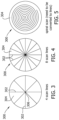
- FIG. 6 shows a schematic section view of the scanned front-end processed wafer 300, taken along one of the diameter lines 302, having the front surface 304 and back surface 308.
- Measurement data that includes surface profiles and thickness profiles of the wafer 300 may be obtained by measuring the surface height H n (x) and thickness T n (x) at points along scanned diameter lines 302 (shown in FIGS. 3 and 4 ) extending across the front surface 304 and, optionally, across the back surface 308.
- the thickness T n (x) at each point is the distance between the point on the front surface 304 and a corresponding point on the back surface 308.
- the thickness plane TP of the wafer 300 can be determined based on the surface height H n (x) and thickness T n (x) at each point.
- the center plane CP of the wafer 300 is determined by regression analysis of the points along the thickness plane TP, as described above.
- the view shown in FIG. 6 is for reference only and is not intended to be a to-scale depiction of the surface height or thickness at points on a measured wafer.
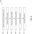
- a raw shape profile is generated for the wafer 300 along each scanned diameter line 302.
- Each raw shape profile is generated based on the obtained measurement data which includes the surface profile and the thickness profile along the respective scanned diameter line 302, and the determined center plane CP of the wafer 300.
- Each raw shape profile includes raw shape values calculated at each scanned point along the respective scanned diameter line 302. The raw shape may be calculated as a function of the surface height H n (x) and the thickness T n (x) at each point, and the height of a corresponding point at the same position on the center plane CP.
- the raw shape profile may be smoothed by moving average.
- defined windows may be set in a direction along the respective scanned diameter line 302 for the raw shape profile.
- the windows may have a size less than 10 mm, less than 5 mm, or 3 mm.
- a moving average of the raw shapes at points within a window is calculated for each window.
- the raw shape for points within each window is then set as the calculated moving average for the window.
- an ideal shape profile is generated for the wafer 300 along each scanned diameter line 302.
- Each ideal shape profile is generated based on polynomial regression of the raw shape profile generated for the respective scanned diameter line 302.
- each ideal shape profile is generated based on 2 nd -order polynomial fitting of the raw shape values calculated at the points along the respective scanned diameter line 302.
- Each ideal shape profile includes ideal shape values calculated at each scanned point along the respective scanned diameter line 302.
- n identifies the scanned diameter line
- x is the relative distance (in mm) of the point from the center 306 of the wafer 300 measured along the scanned diameter line n
- RS n (x) is the raw shape value generated for the scanned diameter line n at x
- a and b are polynomial coefficients
- c is error determined by the polynomial fit analysis.
- the polynomial fit analysis is executed using, for example, NumPy in Python (i.e., np.polyfit curve fitting function).
- a Gapi profile is generated for the wafer 300 along each scanned diameter line 302.
- Each Gapi profile is generated based on the ideal shape profile and the raw shape profile generated for the respective scanned diameter line 302.
- each Gapi profile is generated by generating a delta shape profile for the respective scanned diameter line 302.
- Each delta shape profile includes delta shape values calculated at the points along the respective scanned diameter line 302.
- Each delta shape is calculated by comparing the ideal shape and the raw shape at each point along the respective scanned diameter line 302.
- the delta shape profile is able to describe the wafer shape and flatness for each scanned diameter line 302 by quantifying deviations of each of the generated raw shape profiles from the respective ideal shape profiles.
- each Gapi profile is generated based solely on the delta shape profile generated for the respective scanned diameter line 302.
- Each Gapi profile is based on the delta shape profile generated for the respective scanned diameter line 302 and weighting factors applied to the delta shape profile.
- the weighting factors may be applied (e.g., multiplied with the delta shape values) to account for certain variations (e.g., shape variations and slope changes) of the delta shape profile which may have a larger impact on wafer deformation during processing (e.g., IPD distortion).
- Delta shape profile variations may be quantified as standard variation, variance, or range based on the delta shape value within defined moving windows along a direction of the respective scanned diameter line 302.
- a threshold may be predetermined for the amount of variation tolerated before applying a weighting factor.
- a weighting factor may be applied to each delta shape value within the defined window.
- the weighting factors may be applied based on area variation within defined moving windows along the direction of the respective scanned diameter line 302.
- High variation of area within a relatively narrow window e.g., less than 20 mm
- the area variation may be quantified, for example, as standard variation, variance, or range of the area of delta shape profile within the defined windows.
- fined windows may have a size, for example, less than 20 mm, less than 15 mm, or 11 mm.
- a weighting factor is applied to the delta shape values within a window if the area variation of the delta shape profile in the window is above a predetermined threshold.
- the area variation is quantified as standard variation, and the threshold is equal to or greater than 0.3, equal to or greater than 0.4, or equal to or greater than 0.5.
- the weighting factor in these embodiments may be the standard variation itself. Accordingly, in one example, a weighting factor of 0.4 is applied if the standard deviation is greater than or equal to 0.4 in the defined window, and a weighting factor is not applied (i.e., the weighting factor is zero) if the standard deviation is less than 0.4 in the defined window.
- the weighting factors may also be applied based on slope changes of the delta shape profile within defined moving windows along the direction of the respective scanned diameter line 302.
- Significant turning points of the wafer surface profile within a relatively narrow window e.g., less than 10 mm
- the slope changes of the delta shape profile may be quantified, for example, by comparing the direction and amount of slope in two adjacent defined windows.
- Each adjacent defined window may have a size, for example, less than 20 mm, less than 10 mm, or 5 mm.
- a weighting factor is applied to the delta shape values within the defined windows if the slope change is outside a predetermined threshold.
- the slopes are compared by multiplying the slopes, and the threshold is a negative value (representing a slope change) less than - 0.3, less than -0.35, less than -0.4, less than -0.45, less than -0.5, or less than -0.5.
- the weighting factors in these embodiments may be from more than 1 to 3, or from 1.1 to 2, or from 1.2 to 1.4, or 1.3.
- the weighting factor may be set to 1 if the threshold is not met. Accordingly, in one example, if the slope change is determined to be less than -0.4, a weighting factor of 1.3 is applied, and if the slope change is determined to not be less than -0.4, a weighting factor of 1 is applied.
- Both the area variation and slope changes of the delta shape profiles within defined windows may be used to determine weighting factors applied to the delta shape profiles when generating the Gapi profiles.
- the weighting factors to be applied e.g., multiplied with the delta shape values within the appropriate windows
- SC n (x) is either 1 (default if no weighting factor applied) or greater than 1 (i.e., the determined weighting factor).
- FIGS. 7a and 7b an example set of plots generated using measurement data obtained by a geometry measurement tool (e.g., by scanning the surface 304 of the wafer 300 along scan lines as shown in FIGS. 3-5 ) in accordance with the present disclosure is shown.
- Scan profiles were obtained by scanning a front-end processed wafer surface along 8 diameter lines (indicated as Line:0 - Line:7 in FIGS. 7a and 7b ).
- Raw shape profiles and ideal shape profiles were generated for each scanned diameter line and are shown in each plot.
- Delta shape profiles (not shown) for each diameter line were also generated based on the raw shape and ideal shape profiles as described above.
- Weighting factors were determined in this example based on shape deviations and/or slope changes in the delta shape profile within defined windows.
- the Gapi profile for each diameter line was generated by applying the weighting factors to the delta shape values in the appropriate windows.
- a Gapi value for the wafer is calculated based on the Gapi profiles generated for the scanned diameter lines 302.
- the Gapi value is a global metric which can be used to describe overall variations of wafer flatness and/or shape relative to an ideal plane. It is calculated based on the Gapi profiles as a root-mean-square value of the values included in the Gapi profiles. As such, the Gapi value may also be referred to herein as a "Gapi root-mean-square" or "Gapi rms.”
- a Gapi value calculated for a front-end processed wafer has good correlation with an IPD prediction index provided by a Patterned Wafer Geometry (PWG) metrology system (such as the WaferSight TM PWG5 TM platform manufactured by KLA-Tencor Corporation).
- the PWG metrology system uses raw PWG data obtained from a high accuracy inspection tool (such as a WaferSight TM 2 or 2+ bare wafer metrology system manufactured by KLA-Tencor Corporation) to assess in-process wafer distortion based on changes in wafer shape and predict overlay error.
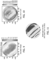
- FIG. 9 shows a contour map of the raw localized shape features of a front-end processed wafer. As shown in FIGS.
- contour maps of the Gapi profiles generated for the front-end processed wafer ( FIG. 10 ) and the IPD map generated using the PWG metrology system based on in-process wafer data ( FIG. 11 ) indicate that IPD may be predicted based on the Gapi profiles generated for the front-end processed wafer. More specifically, the generated Gapi profile features of the wafer of FIG. 10 (with a Gapi value of 4.324) correlate well with the calculated IPD site mean root-mean-square metrics and the IPD map of FIG. 11 of the same wafer (having the localized shape features shown in FIG. 9 ), where the IPD metrics and IPD map are determined after a final polishing step.
- FIG. 12 shows that the calculated global metrics (both taken as a root-mean-square of the local values) of the Gapi profiles and the IPD values have a strong correlation, with a R 2 value of greater than 0.7 for various wafer shapes.
- Front-end processed wafers are sorted (such as at step 206 in process 200) if the calculated Gapi value of the wafer does not meet a predetermined threshold.
- the threshold may be set to Gapi value that correlates with a high back-end yield percentage (e.g., greater than 50%, greater than 60%, or greater than 70%).
- advantages such as higher back-end yield, reducing the need for overlay error control, and salvaging of poorer quality wafers can be achieved.
- a wafer is processed by a front-end process tool (e.g., front-end process tool 702 shown in FIG. 27 ).
- a wafer may be sliced from a single crystal ingot of semiconductor material (e.g., silicon) using a wire saw.
- the wafer may also be brought to a desired thickness using a front-end process tool such as a lapping tool or a grinding tool.
- a Gapi value of the front-end processed (e.g., wire sawed, lapped and/or grinded) wafer is calculated in accordance with the present disclosure (e.g., by process 400 shown in FIG. 8 ).
- the Gapi value is compared to a predetermined threshold value.
- the predetermined threshold value may be based on historical data which correlates a Gapi value to a back-end yield percentage.
- the threshold may be set to a Gapi value which correlates with a back-end yield percentage of greater than 50%.
- the threshold is set based on the data shown in the graph of FIG. 13 .
- the predetermined threshold of the Gapi value is less than 6, less than 5.5, less than 5, less than 4.5, such as less than 4, or less than 3.5. If the Gapi value is less than or equal to the threshold Gapi value, such as less than or equal to 5, then the front-end processed wafer is sorted for polishing at step 508.
- FIGS. 15-18 show a contour map of the raw localized shape features ( FIG. 15 ), a chart of the raw shape profile, ideal shape profile, and the Gapi profile plots for a single scanned diameter line ( FIG. 16 ), a contour map of the Gapi profiles ( FIG. 17 ), and an IPD contour map ( FIG. 18 ), of a front-end processed wafer having a Gapi value of 5.41, which in this exemplary embodiment is greater than a predetermined threshold for step 506 of process flow 500. Accordingly, the front-end processed wafer of FIGS. 15-18 is not sorted for polishing at step 508.
- one or more front-end process tools are tuned (e.g., modified and/or adjusted) based on at least one of the Gapi profiles used to calculate the Gapi value shown in FIG. 17 , such as the Gapi profile shown in FIG. 16 .
- a wire saw may be tuned based on at least one Gapi profile of the wafer.
- the Gapi profile plot in FIG. 16 shows the Gapi profile of the diameter line (i.e., Line:5) of the wafer that is parallel (or substantially parallel) to the cutting direction of the wire saw. It is observed that relatively high Gapi values of the Gapi profile are located at certain points along the diameter line in a direction of the scanned diameter line, which as shown in FIG.
- the wire saw may be tuned to correct the high variations at these points. For example, the value of the slurry temperature or the bearing temperature at positions corresponding to these high variation points near the radial edge of the wafer may be adjusted to provide a smoother wafer shape upon the entrance and exit of the wire as the wafer is cut from a single crystal ingot.
- FIGS. 19-22 show a contour map of the raw localized shape features ( FIG. 19 ), a chart of the raw shape profile, ideal shape profile, and the Gapi profile plots for a single scanned diameter line ( FIG. 20 ), a contour map of the Gapi profiles ( FIG. 21 ), and an IPD contour map ( FIG. 22 ), of a second front-end processed wafer after the front-end process tool is tuned based on the observations from FIGS. 15-18 . As shown in FIGS.
- the tuning of the front-end process tool results in the second front-end processed wafer with improved Gapi profiles (with less variation at the radial edges), as well as a lower Gapi value (3.42) and IPD mean root-mean-square value (16.45).
- the second front-end processed wafer provided after the tuning step may be the same wafer processed at step 502, which has been salvaged by repeating the front-end process step.
- the second front-end processed wafer processed by the tuned front-end tool may also be a different wafer.
- One advantage of the process 500 is that adjustments and/or modifications of the front-end tool may be made more quickly and efficiently using a metric that is generated and/or calculated early on in the wafering process (e.g., before polishing).
- a metric that is generated and/or calculated early on in the wafering process (e.g., before polishing).
- Existing metrics used to predict wafer deformation during fabrication require the wafer be polished in order to obtain high quality shape and/or flatness data of the wafer.
- Process anomalies in front-end tools e.g., wire saw, lapping tool, or grinding tool
- significant time passes hours, days, weeks between the front-end processing and the polishing of a given wafer.
- process 500 provides a significant improvement by providing early detection of process anomalies in the front-end process which can be fixed by tuning the front-end tool(s) and thereby impact fewer wafers.
- Gapi edge metrics may be used to characterize wafer edge profiles. Wafer edge conditions are known to significantly impact the edge die yield. For example, issues associated with film layer peeling (i.e., delamination), particle contamination, and photoresist coating offset error, each of which negatively impact edge die yield, are known to arise from wafer edge defects. Using Gapi edge metrics in accordance with the present disclosure can ensure wafers with sufficiently smooth edges are fabricated and therefore provide similar improvements in back-end yield as discussed above with respect to Gapi metrics.
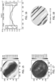
- a process 600 for calculating Gapi edge values of a front-end processed wafer is shown.
- measurement data of an edge profile of the front-end processed wafer is obtained.
- the edge profile data may be obtained using commercial 3D microscopes such as by coherence scanning interferometric, confocal laser scanning, or laser scanning microscopes (such as those manufactured by Zygo, Olympus, or Keyence).
- the measured wafer may be in an unchucked (i.e., free-standing) state.
- a simplification algorithm is used to convert the edge profile data into a simplified curve by reducing the set of points included in the edge profile.
- a simplified curve of the edge profile data may be generated based on the Ramer-Douglas-Peucker algorithm (i.e., the iterative end-point fit algorithm).
- the amount of points comprising the edge profile may be set by tuning the epsilon ( ⁇ ) parameter used in the Ramer-Douglas-Peucker algorithm, as is understood by those skilled in the art.
- ⁇ is tuned to reduce the numbers of the curve to 3 points.
- the profile center point is determined as the mid-point on the simplified curve.
- the profile center point is determined as the middle of the 3 points on the simplified curve in one example.
- a Gapi edge value for the wafer is calculated based on the Gapi edge profile of the wafer edge.
- the Gapi edge value is a global metric which can be used to describe overall variations of the wafer edge profile to an ideal plane.
- the Gapi edge value is calculated based on the Gapi edge profile as, for example, a root-mean-square value (also referred to as a "Gapi edge root-mean-square” or "Gapi edge rms") of the values comprising the Gapi edge profile.
- the Gapi edge value is calculated as the maximum edge value (also referred to as a "Gapi edge maximum value" or "Gapi edge max”) of the Gapi edge profile.
Landscapes
- Engineering & Computer Science (AREA)
- Mechanical Engineering (AREA)
- Chemical & Material Sciences (AREA)
- Physics & Mathematics (AREA)
- General Physics & Mathematics (AREA)
- Ceramic Engineering (AREA)
- Inorganic Chemistry (AREA)
- Signal Processing (AREA)
- Computer Vision & Pattern Recognition (AREA)
- Health & Medical Sciences (AREA)
- Life Sciences & Earth Sciences (AREA)
- Analytical Chemistry (AREA)
- Biochemistry (AREA)
- General Health & Medical Sciences (AREA)
- Immunology (AREA)
- Pathology (AREA)
- Testing Or Measuring Of Semiconductors Or The Like (AREA)
- Mechanical Treatment Of Semiconductor (AREA)
- Length Measuring Devices With Unspecified Measuring Means (AREA)
Priority Applications (1)
| Application Number | Priority Date | Filing Date | Title |
|---|---|---|---|
| EP25174400.9A EP4576178A3 (en) | 2021-08-16 | 2022-08-09 | Systems and methods for processing semiconductor wafers using front-end processed wafer geometry metrics |
Applications Claiming Priority (2)
| Application Number | Priority Date | Filing Date | Title |
|---|---|---|---|
| US202163260295P | 2021-08-16 | 2021-08-16 | |
| PCT/US2022/039785 WO2023022898A1 (en) | 2021-08-16 | 2022-08-09 | Systems and methods for processing semiconductor wafers using front-end processed wafer geometry metrics |
Related Child Applications (2)
| Application Number | Title | Priority Date | Filing Date |
|---|---|---|---|
| EP25174400.9A Division EP4576178A3 (en) | 2021-08-16 | 2022-08-09 | Systems and methods for processing semiconductor wafers using front-end processed wafer geometry metrics |
| EP25174400.9A Division-Into EP4576178A3 (en) | 2021-08-16 | 2022-08-09 | Systems and methods for processing semiconductor wafers using front-end processed wafer geometry metrics |
Publications (2)
| Publication Number | Publication Date |
|---|---|
| EP4388579A1 EP4388579A1 (en) | 2024-06-26 |
| EP4388579B1 true EP4388579B1 (en) | 2025-06-25 |
Family
ID=83188446
Family Applications (2)
| Application Number | Title | Priority Date | Filing Date |
|---|---|---|---|
| EP22764521.5A Active EP4388579B1 (en) | 2021-08-16 | 2022-08-09 | Systems and methods for processing semiconductor wafers using front-end processed wafer geometry metrics |
| EP25174400.9A Pending EP4576178A3 (en) | 2021-08-16 | 2022-08-09 | Systems and methods for processing semiconductor wafers using front-end processed wafer geometry metrics |
Family Applications After (1)
| Application Number | Title | Priority Date | Filing Date |
|---|---|---|---|
| EP25174400.9A Pending EP4576178A3 (en) | 2021-08-16 | 2022-08-09 | Systems and methods for processing semiconductor wafers using front-end processed wafer geometry metrics |
Country Status (7)
| Country | Link |
|---|---|
| US (3) | US12385850B2 (enExample) |
| EP (2) | EP4388579B1 (enExample) |
| JP (2) | JP7760704B2 (enExample) |
| KR (2) | KR20250124260A (enExample) |
| CN (1) | CN117999643A (enExample) |
| TW (1) | TW202544952A (enExample) |
| WO (1) | WO2023022898A1 (enExample) |
Families Citing this family (3)
| Publication number | Priority date | Publication date | Assignee | Title |
|---|---|---|---|---|
| US12385850B2 (en) * | 2021-08-16 | 2025-08-12 | Globalwafers Co., Ltd. | Semiconductor wafers using front-end processed wafer global geometry metrics |
| US20250290745A1 (en) * | 2024-03-15 | 2025-09-18 | Tokyo Electron Limited | Apparatus and method for determining the surface profile of a semiconductor substrate using a laser scanning technique |
| WO2026015590A1 (en) | 2024-07-10 | 2026-01-15 | Globalwafers Co., Ltd. | Systems and methods for analyzing nanotopography of front-end processed semiconductor wafers |
Family Cites Families (15)
| Publication number | Priority date | Publication date | Assignee | Title |
|---|---|---|---|---|
| JP3838341B2 (ja) * | 2001-09-14 | 2006-10-25 | 信越半導体株式会社 | ウェーハの形状評価方法及びウェーハ並びにウェーハの選別方法 |
| US9102033B2 (en) | 2010-11-24 | 2015-08-11 | Taiwan Semiconductor Manufacturing Company, Ltd. | Apparatus and method for target thickness and surface profile uniformity control of multi-head chemical mechanical polishing process |
| JP2012117811A (ja) * | 2010-11-29 | 2012-06-21 | Kunitoshi Nishimura | ウエハ平坦度測定法 |
| WO2013178459A1 (en) | 2012-05-31 | 2013-12-05 | Asml Netherlands B.V. | Gradient-based pattern and evaluation point selection |
| US20140078495A1 (en) | 2012-09-14 | 2014-03-20 | Stmicroelectronics, Inc. | Inline metrology for attaining full wafer map of uniformity and surface charge |
| US9430593B2 (en) | 2012-10-11 | 2016-08-30 | Kla-Tencor Corporation | System and method to emulate finite element model based prediction of in-plane distortions due to semiconductor wafer chucking |
| US10401279B2 (en) | 2013-10-29 | 2019-09-03 | Kla-Tencor Corporation | Process-induced distortion prediction and feedforward and feedback correction of overlay errors |
| US9645097B2 (en) * | 2014-06-20 | 2017-05-09 | Kla-Tencor Corporation | In-line wafer edge inspection, wafer pre-alignment, and wafer cleaning |
| KR102184033B1 (ko) | 2014-06-24 | 2020-11-27 | 케이엘에이 코포레이션 | 반도체 프로세스 제어를 위한 패터닝된 웨이퍼 지오메트리 측정 |
| US9870928B2 (en) | 2014-10-31 | 2018-01-16 | Veeco Precision Surface Processing Llc | System and method for updating an arm scan profile through a graphical user interface |
| US10024654B2 (en) | 2015-04-06 | 2018-07-17 | Kla-Tencor Corporation | Method and system for determining in-plane distortions in a substrate |
| KR102620998B1 (ko) * | 2018-05-25 | 2024-01-04 | 삼성전자주식회사 | 기판 검사 방법, 기판 처리 방법 및 이를 수행하기 위한 기판 처리 시스템 |
| WO2020043525A1 (en) * | 2018-08-28 | 2020-03-05 | Asml Netherlands B.V. | Systems and methods of optimal metrology guidance |
| JP6899080B2 (ja) * | 2018-09-05 | 2021-07-07 | 信越半導体株式会社 | ウェーハ形状データ化方法 |
| US12385850B2 (en) * | 2021-08-16 | 2025-08-12 | Globalwafers Co., Ltd. | Semiconductor wafers using front-end processed wafer global geometry metrics |
-
2022
- 2022-08-08 US US17/818,123 patent/US12385850B2/en active Active
- 2022-08-08 US US17/818,131 patent/US12487185B2/en active Active
- 2022-08-09 WO PCT/US2022/039785 patent/WO2023022898A1/en not_active Ceased
- 2022-08-09 KR KR1020257026342A patent/KR20250124260A/ko active Pending
- 2022-08-09 EP EP22764521.5A patent/EP4388579B1/en active Active
- 2022-08-09 KR KR1020247008533A patent/KR20240043802A/ko active Pending
- 2022-08-09 CN CN202280063700.8A patent/CN117999643A/zh active Pending
- 2022-08-09 EP EP25174400.9A patent/EP4576178A3/en active Pending
- 2022-08-09 JP JP2024509126A patent/JP7760704B2/ja active Active
- 2022-08-15 TW TW114129807A patent/TW202544952A/zh unknown
-
2025
- 2025-08-14 JP JP2025135179A patent/JP2025166173A/ja active Pending
- 2025-11-06 US US19/381,497 patent/US20260063568A1/en active Pending
Also Published As
| Publication number | Publication date |
|---|---|
| EP4576178A2 (en) | 2025-06-25 |
| US12385850B2 (en) | 2025-08-12 |
| TW202329278A (zh) | 2023-07-16 |
| TW202544952A (zh) | 2025-11-16 |
| JP2025166173A (ja) | 2025-11-05 |
| EP4388579A1 (en) | 2024-06-26 |
| KR20240043802A (ko) | 2024-04-03 |
| JP7760704B2 (ja) | 2025-10-27 |
| US20230047412A1 (en) | 2023-02-16 |
| EP4576178A3 (en) | 2025-09-10 |
| US20260063568A1 (en) | 2026-03-05 |
| WO2023022898A1 (en) | 2023-02-23 |
| US12487185B2 (en) | 2025-12-02 |
| US20230050442A1 (en) | 2023-02-16 |
| JP2024534046A (ja) | 2024-09-18 |
| KR20250124260A (ko) | 2025-08-19 |
| CN117999643A (zh) | 2024-05-07 |
Similar Documents
| Publication | Publication Date | Title |
|---|---|---|
| US20260063568A1 (en) | Systems and methods for processing semiconductor wafers using front-end processed wafer global geometry metrics | |
| JP4464033B2 (ja) | 半導体ウエーハの形状評価方法及び形状評価装置 | |
| US6975960B2 (en) | Method for evaluating wafer configuration, wafer, and wafer sorting method | |
| CN104428882B (zh) | 半导体晶片的评价方法及制造方法 | |
| JP4400331B2 (ja) | ウエーハの形状評価方法及び管理方法 | |
| JP3982336B2 (ja) | 半導体ウエーハの加工方法及びプラズマエッチング装置 | |
| CN114667594A (zh) | 晶片的研磨方法及硅晶片 | |
| JP5074845B2 (ja) | 半導体ウェハの研削方法、及び半導体ウェハの加工方法 | |
| JP4606231B2 (ja) | 半導体ウエーハの評価方法及び評価装置並びに半導体ウエーハの製造方法 | |
| KR20050002801A (ko) | 반도체 웨이퍼 | |
| TWI921592B (zh) | 使用經前端處理之晶圓之幾何度量來處理半導體晶圓之系統及方法 | |
| US20260018467A1 (en) | Systems and methods for analyzing nanotopography of front-end processed semiconductor wafers | |
| CN117121166A (zh) | 半导体晶圆的制造方法 | |
| US20250273519A1 (en) | Systems and methods for processing semiconductor wafers using near edge region roundness | |
| TW202607848A (zh) | 用於分析經前段處理之半導體晶圓之奈米形貌之系統及方法 | |
| WO2026015756A1 (en) | Systems and methods for regression filters and zero edge exclusion filters |
Legal Events
| Date | Code | Title | Description |
|---|---|---|---|
| STAA | Information on the status of an ep patent application or granted ep patent |
Free format text: STATUS: UNKNOWN |
|
| STAA | Information on the status of an ep patent application or granted ep patent |
Free format text: STATUS: THE INTERNATIONAL PUBLICATION HAS BEEN MADE |
|
| PUAI | Public reference made under article 153(3) epc to a published international application that has entered the european phase |
Free format text: ORIGINAL CODE: 0009012 |
|
| STAA | Information on the status of an ep patent application or granted ep patent |
Free format text: STATUS: REQUEST FOR EXAMINATION WAS MADE |
|
| 17P | Request for examination filed |
Effective date: 20240307 |
|
| AK | Designated contracting states |
Kind code of ref document: A1 Designated state(s): AL AT BE BG CH CY CZ DE DK EE ES FI FR GB GR HR HU IE IS IT LI LT LU LV MC MK MT NL NO PL PT RO RS SE SI SK SM TR |
|
| DAV | Request for validation of the european patent (deleted) | ||
| DAX | Request for extension of the european patent (deleted) | ||
| GRAP | Despatch of communication of intention to grant a patent |
Free format text: ORIGINAL CODE: EPIDOSNIGR1 |
|
| STAA | Information on the status of an ep patent application or granted ep patent |
Free format text: STATUS: GRANT OF PATENT IS INTENDED |
|
| INTG | Intention to grant announced |
Effective date: 20250122 |
|
| GRAS | Grant fee paid |
Free format text: ORIGINAL CODE: EPIDOSNIGR3 |
|
| GRAA | (expected) grant |
Free format text: ORIGINAL CODE: 0009210 |
|
| STAA | Information on the status of an ep patent application or granted ep patent |
Free format text: STATUS: THE PATENT HAS BEEN GRANTED |
|
| AK | Designated contracting states |
Kind code of ref document: B1 Designated state(s): AL AT BE BG CH CY CZ DE DK EE ES FI FR GB GR HR HU IE IS IT LI LT LU LV MC MK MT NL NO PL PT RO RS SE SI SK SM TR |
|
| REG | Reference to a national code |
Ref country code: GB Ref legal event code: FG4D |
|
| REG | Reference to a national code |
Ref country code: CH Ref legal event code: EP |
|
| REG | Reference to a national code |
Ref country code: DE Ref legal event code: R096 Ref document number: 602022016547 Country of ref document: DE |
|
| REG | Reference to a national code |
Ref country code: CH Ref legal event code: EP |
|
| REG | Reference to a national code |
Ref country code: IE Ref legal event code: FG4D |
|
| PG25 | Lapsed in a contracting state [announced via postgrant information from national office to epo] |
Ref country code: FI Free format text: LAPSE BECAUSE OF FAILURE TO SUBMIT A TRANSLATION OF THE DESCRIPTION OR TO PAY THE FEE WITHIN THE PRESCRIBED TIME-LIMIT Effective date: 20250625 |
|
| PGFP | Annual fee paid to national office [announced via postgrant information from national office to epo] |
Ref country code: DE Payment date: 20250827 Year of fee payment: 4 |
|
| REG | Reference to a national code |
Ref country code: LT Ref legal event code: MG9D |
|
| PG25 | Lapsed in a contracting state [announced via postgrant information from national office to epo] |
Ref country code: GR Free format text: LAPSE BECAUSE OF FAILURE TO SUBMIT A TRANSLATION OF THE DESCRIPTION OR TO PAY THE FEE WITHIN THE PRESCRIBED TIME-LIMIT Effective date: 20250926 Ref country code: NO Free format text: LAPSE BECAUSE OF FAILURE TO SUBMIT A TRANSLATION OF THE DESCRIPTION OR TO PAY THE FEE WITHIN THE PRESCRIBED TIME-LIMIT Effective date: 20250925 |
|
| PG25 | Lapsed in a contracting state [announced via postgrant information from national office to epo] |
Ref country code: BG Free format text: LAPSE BECAUSE OF FAILURE TO SUBMIT A TRANSLATION OF THE DESCRIPTION OR TO PAY THE FEE WITHIN THE PRESCRIBED TIME-LIMIT Effective date: 20250625 |
|
| PG25 | Lapsed in a contracting state [announced via postgrant information from national office to epo] |
Ref country code: HR Free format text: LAPSE BECAUSE OF FAILURE TO SUBMIT A TRANSLATION OF THE DESCRIPTION OR TO PAY THE FEE WITHIN THE PRESCRIBED TIME-LIMIT Effective date: 20250625 |
|
| PGFP | Annual fee paid to national office [announced via postgrant information from national office to epo] |
Ref country code: AT Payment date: 20251020 Year of fee payment: 4 Ref country code: FR Payment date: 20250825 Year of fee payment: 4 |
|
| PG25 | Lapsed in a contracting state [announced via postgrant information from national office to epo] |
Ref country code: RS Free format text: LAPSE BECAUSE OF FAILURE TO SUBMIT A TRANSLATION OF THE DESCRIPTION OR TO PAY THE FEE WITHIN THE PRESCRIBED TIME-LIMIT Effective date: 20250925 |
|
| PG25 | Lapsed in a contracting state [announced via postgrant information from national office to epo] |
Ref country code: LV Free format text: LAPSE BECAUSE OF FAILURE TO SUBMIT A TRANSLATION OF THE DESCRIPTION OR TO PAY THE FEE WITHIN THE PRESCRIBED TIME-LIMIT Effective date: 20250625 |
|
| REG | Reference to a national code |
Ref country code: NL Ref legal event code: MP Effective date: 20250625 |
|
| PG25 | Lapsed in a contracting state [announced via postgrant information from national office to epo] |
Ref country code: NL Free format text: LAPSE BECAUSE OF FAILURE TO SUBMIT A TRANSLATION OF THE DESCRIPTION OR TO PAY THE FEE WITHIN THE PRESCRIBED TIME-LIMIT Effective date: 20250625 |
|
| REG | Reference to a national code |
Ref country code: DE Ref legal event code: R079 Ref document number: 602022016547 Country of ref document: DE Free format text: PREVIOUS MAIN CLASS: H01L0021660000 Ipc: H10P0074000000 |
|
| PG25 | Lapsed in a contracting state [announced via postgrant information from national office to epo] |
Ref country code: PT Free format text: LAPSE BECAUSE OF FAILURE TO SUBMIT A TRANSLATION OF THE DESCRIPTION OR TO PAY THE FEE WITHIN THE PRESCRIBED TIME-LIMIT Effective date: 20251027 |
|
| REG | Reference to a national code |
Ref country code: AT Ref legal event code: MK05 Ref document number: 1807490 Country of ref document: AT Kind code of ref document: T Effective date: 20250625 |
|
| PG25 | Lapsed in a contracting state [announced via postgrant information from national office to epo] |
Ref country code: IS Free format text: LAPSE BECAUSE OF FAILURE TO SUBMIT A TRANSLATION OF THE DESCRIPTION OR TO PAY THE FEE WITHIN THE PRESCRIBED TIME-LIMIT Effective date: 20251025 |
|
| PG25 | Lapsed in a contracting state [announced via postgrant information from national office to epo] |
Ref country code: AT Free format text: LAPSE BECAUSE OF FAILURE TO SUBMIT A TRANSLATION OF THE DESCRIPTION OR TO PAY THE FEE WITHIN THE PRESCRIBED TIME-LIMIT Effective date: 20250625 Ref country code: SM Free format text: LAPSE BECAUSE OF FAILURE TO SUBMIT A TRANSLATION OF THE DESCRIPTION OR TO PAY THE FEE WITHIN THE PRESCRIBED TIME-LIMIT Effective date: 20250625 |
|
| PG25 | Lapsed in a contracting state [announced via postgrant information from national office to epo] |
Ref country code: CZ Free format text: LAPSE BECAUSE OF FAILURE TO SUBMIT A TRANSLATION OF THE DESCRIPTION OR TO PAY THE FEE WITHIN THE PRESCRIBED TIME-LIMIT Effective date: 20250625 |
|
| PG25 | Lapsed in a contracting state [announced via postgrant information from national office to epo] |
Ref country code: PL Free format text: LAPSE BECAUSE OF FAILURE TO SUBMIT A TRANSLATION OF THE DESCRIPTION OR TO PAY THE FEE WITHIN THE PRESCRIBED TIME-LIMIT Effective date: 20250625 |
|
| PG25 | Lapsed in a contracting state [announced via postgrant information from national office to epo] |
Ref country code: EE Free format text: LAPSE BECAUSE OF FAILURE TO SUBMIT A TRANSLATION OF THE DESCRIPTION OR TO PAY THE FEE WITHIN THE PRESCRIBED TIME-LIMIT Effective date: 20250625 |
|
| PG25 | Lapsed in a contracting state [announced via postgrant information from national office to epo] |
Ref country code: SK Free format text: LAPSE BECAUSE OF FAILURE TO SUBMIT A TRANSLATION OF THE DESCRIPTION OR TO PAY THE FEE WITHIN THE PRESCRIBED TIME-LIMIT Effective date: 20250625 |
|
| PG25 | Lapsed in a contracting state [announced via postgrant information from national office to epo] |
Ref country code: ES Free format text: LAPSE BECAUSE OF FAILURE TO SUBMIT A TRANSLATION OF THE DESCRIPTION OR TO PAY THE FEE WITHIN THE PRESCRIBED TIME-LIMIT Effective date: 20250625 |
|
| PG25 | Lapsed in a contracting state [announced via postgrant information from national office to epo] |
Ref country code: RO Free format text: LAPSE BECAUSE OF FAILURE TO SUBMIT A TRANSLATION OF THE DESCRIPTION OR TO PAY THE FEE WITHIN THE PRESCRIBED TIME-LIMIT Effective date: 20250625 |
|
| REG | Reference to a national code |
Ref country code: CH Ref legal event code: H13 Free format text: ST27 STATUS EVENT CODE: U-0-0-H10-H13 (AS PROVIDED BY THE NATIONAL OFFICE) Effective date: 20260324 |
|
| PG25 | Lapsed in a contracting state [announced via postgrant information from national office to epo] |
Ref country code: MC Free format text: LAPSE BECAUSE OF FAILURE TO SUBMIT A TRANSLATION OF THE DESCRIPTION OR TO PAY THE FEE WITHIN THE PRESCRIBED TIME-LIMIT Effective date: 20250625 |
|
| PG25 | Lapsed in a contracting state [announced via postgrant information from national office to epo] |
Ref country code: DK Free format text: LAPSE BECAUSE OF FAILURE TO SUBMIT A TRANSLATION OF THE DESCRIPTION OR TO PAY THE FEE WITHIN THE PRESCRIBED TIME-LIMIT Effective date: 20250625 |
|
| PG25 | Lapsed in a contracting state [announced via postgrant information from national office to epo] |
Ref country code: IT Free format text: LAPSE BECAUSE OF FAILURE TO SUBMIT A TRANSLATION OF THE DESCRIPTION OR TO PAY THE FEE WITHIN THE PRESCRIBED TIME-LIMIT Effective date: 20250625 Ref country code: LU Free format text: LAPSE BECAUSE OF NON-PAYMENT OF DUE FEES Effective date: 20250809 |
|
| PG25 | Lapsed in a contracting state [announced via postgrant information from national office to epo] |
Ref country code: CH Free format text: LAPSE BECAUSE OF NON-PAYMENT OF DUE FEES Effective date: 20250831 |
|
| PLBE | No opposition filed within time limit |
Free format text: ORIGINAL CODE: 0009261 |
|
| STAA | Information on the status of an ep patent application or granted ep patent |
Free format text: STATUS: NO OPPOSITION FILED WITHIN TIME LIMIT |