EP4387410A1 - Transistor arrays with controllable gate voltage - Google Patents
Transistor arrays with controllable gate voltage Download PDFInfo
- Publication number
- EP4387410A1 EP4387410A1 EP23197413.0A EP23197413A EP4387410A1 EP 4387410 A1 EP4387410 A1 EP 4387410A1 EP 23197413 A EP23197413 A EP 23197413A EP 4387410 A1 EP4387410 A1 EP 4387410A1
- Authority
- EP
- European Patent Office
- Prior art keywords
- semiconductor layer
- field
- layer
- gate electrode
- effect transistor
- Prior art date
- Legal status (The legal status is an assumption and is not a legal conclusion. Google has not performed a legal analysis and makes no representation as to the accuracy of the status listed.)
- Granted
Links
Images






Classifications
-
- H—ELECTRICITY
- H10—SEMICONDUCTOR DEVICES; ELECTRIC SOLID-STATE DEVICES NOT OTHERWISE PROVIDED FOR
- H10B—ELECTRONIC MEMORY DEVICES
- H10B63/00—Resistance change memory devices, e.g. resistive RAM [ReRAM] devices
- H10B63/30—Resistance change memory devices, e.g. resistive RAM [ReRAM] devices comprising selection components having three or more electrodes, e.g. transistors
-
- H—ELECTRICITY
- H10—SEMICONDUCTOR DEVICES; ELECTRIC SOLID-STATE DEVICES NOT OTHERWISE PROVIDED FOR
- H10D—INORGANIC ELECTRIC SEMICONDUCTOR DEVICES
- H10D84/00—Integrated devices formed in or on semiconductor substrates that comprise only semiconducting layers, e.g. on Si wafers or on GaAs-on-Si wafers
- H10D84/01—Manufacture or treatment
- H10D84/02—Manufacture or treatment characterised by using material-based technologies
- H10D84/03—Manufacture or treatment characterised by using material-based technologies using Group IV technology, e.g. silicon technology or silicon-carbide [SiC] technology
- H10D84/038—Manufacture or treatment characterised by using material-based technologies using Group IV technology, e.g. silicon technology or silicon-carbide [SiC] technology using silicon technology, e.g. SiGe
-
- H—ELECTRICITY
- H10—SEMICONDUCTOR DEVICES; ELECTRIC SOLID-STATE DEVICES NOT OTHERWISE PROVIDED FOR
- H10B—ELECTRONIC MEMORY DEVICES
- H10B63/00—Resistance change memory devices, e.g. resistive RAM [ReRAM] devices
- H10B63/30—Resistance change memory devices, e.g. resistive RAM [ReRAM] devices comprising selection components having three or more electrodes, e.g. transistors
- H10B63/34—Resistance change memory devices, e.g. resistive RAM [ReRAM] devices comprising selection components having three or more electrodes, e.g. transistors of the vertical channel field-effect transistor type
-
- H—ELECTRICITY
- H10—SEMICONDUCTOR DEVICES; ELECTRIC SOLID-STATE DEVICES NOT OTHERWISE PROVIDED FOR
- H10B—ELECTRONIC MEMORY DEVICES
- H10B63/00—Resistance change memory devices, e.g. resistive RAM [ReRAM] devices
- H10B63/80—Arrangements comprising multiple bistable or multi-stable switching components of the same type on a plane parallel to the substrate, e.g. cross-point arrays
-
- H—ELECTRICITY
- H10—SEMICONDUCTOR DEVICES; ELECTRIC SOLID-STATE DEVICES NOT OTHERWISE PROVIDED FOR
- H10D—INORGANIC ELECTRIC SEMICONDUCTOR DEVICES
- H10D64/00—Electrodes of devices having potential barriers
- H10D64/20—Electrodes characterised by their shapes, relative sizes or dispositions
- H10D64/27—Electrodes not carrying the current to be rectified, amplified, oscillated or switched, e.g. gates
- H10D64/311—Gate electrodes for field-effect devices
- H10D64/411—Gate electrodes for field-effect devices for FETs
-
- H—ELECTRICITY
- H10—SEMICONDUCTOR DEVICES; ELECTRIC SOLID-STATE DEVICES NOT OTHERWISE PROVIDED FOR
- H10D—INORGANIC ELECTRIC SEMICONDUCTOR DEVICES
- H10D64/00—Electrodes of devices having potential barriers
- H10D64/60—Electrodes characterised by their materials
- H10D64/66—Electrodes having a conductor capacitively coupled to a semiconductor by an insulator, e.g. MIS electrodes
- H10D64/661—Electrodes having a conductor capacitively coupled to a semiconductor by an insulator, e.g. MIS electrodes the conductor comprising a layer of silicon contacting the insulator, e.g. polysilicon having vertical doping variation
- H10D64/662—Electrodes having a conductor capacitively coupled to a semiconductor by an insulator, e.g. MIS electrodes the conductor comprising a layer of silicon contacting the insulator, e.g. polysilicon having vertical doping variation the conductor further comprising additional layers, e.g. multiple silicon layers having different crystal structures
- H10D64/663—Electrodes having a conductor capacitively coupled to a semiconductor by an insulator, e.g. MIS electrodes the conductor comprising a layer of silicon contacting the insulator, e.g. polysilicon having vertical doping variation the conductor further comprising additional layers, e.g. multiple silicon layers having different crystal structures the additional layers comprising a silicide layer contacting the layer of silicon, e.g. polycide gates
-
- H—ELECTRICITY
- H10—SEMICONDUCTOR DEVICES; ELECTRIC SOLID-STATE DEVICES NOT OTHERWISE PROVIDED FOR
- H10D—INORGANIC ELECTRIC SEMICONDUCTOR DEVICES
- H10D84/00—Integrated devices formed in or on semiconductor substrates that comprise only semiconducting layers, e.g. on Si wafers or on GaAs-on-Si wafers
- H10D84/01—Manufacture or treatment
- H10D84/0123—Integrating together multiple components covered by H10D12/00 or H10D30/00, e.g. integrating multiple IGBTs
- H10D84/0126—Integrating together multiple components covered by H10D12/00 or H10D30/00, e.g. integrating multiple IGBTs the components including insulated gates, e.g. IGFETs
- H10D84/0149—Manufacturing their interconnections or electrodes, e.g. source or drain electrodes
-
- H—ELECTRICITY
- H10—SEMICONDUCTOR DEVICES; ELECTRIC SOLID-STATE DEVICES NOT OTHERWISE PROVIDED FOR
- H10D—INORGANIC ELECTRIC SEMICONDUCTOR DEVICES
- H10D86/00—Integrated devices formed in or on insulating or conducting substrates, e.g. formed in silicon-on-insulator [SOI] substrates or on stainless steel or glass substrates
- H10D86/01—Manufacture or treatment
- H10D86/021—Manufacture or treatment of multiple TFTs
-
- H—ELECTRICITY
- H10—SEMICONDUCTOR DEVICES; ELECTRIC SOLID-STATE DEVICES NOT OTHERWISE PROVIDED FOR
- H10D—INORGANIC ELECTRIC SEMICONDUCTOR DEVICES
- H10D86/00—Integrated devices formed in or on insulating or conducting substrates, e.g. formed in silicon-on-insulator [SOI] substrates or on stainless steel or glass substrates
- H10D86/40—Integrated devices formed in or on insulating or conducting substrates, e.g. formed in silicon-on-insulator [SOI] substrates or on stainless steel or glass substrates characterised by multiple TFTs
- H10D86/421—Integrated devices formed in or on insulating or conducting substrates, e.g. formed in silicon-on-insulator [SOI] substrates or on stainless steel or glass substrates characterised by multiple TFTs having a particular composition, shape or crystalline structure of the active layer
-
- H—ELECTRICITY
- H10—SEMICONDUCTOR DEVICES; ELECTRIC SOLID-STATE DEVICES NOT OTHERWISE PROVIDED FOR
- H10D—INORGANIC ELECTRIC SEMICONDUCTOR DEVICES
- H10D86/00—Integrated devices formed in or on insulating or conducting substrates, e.g. formed in silicon-on-insulator [SOI] substrates or on stainless steel or glass substrates
- H10D86/40—Integrated devices formed in or on insulating or conducting substrates, e.g. formed in silicon-on-insulator [SOI] substrates or on stainless steel or glass substrates characterised by multiple TFTs
- H10D86/60—Integrated devices formed in or on insulating or conducting substrates, e.g. formed in silicon-on-insulator [SOI] substrates or on stainless steel or glass substrates characterised by multiple TFTs wherein the TFTs are in active matrices
-
- H—ELECTRICITY
- H10—SEMICONDUCTOR DEVICES; ELECTRIC SOLID-STATE DEVICES NOT OTHERWISE PROVIDED FOR
- H10W—GENERIC PACKAGES, INTERCONNECTIONS, CONNECTORS OR OTHER CONSTRUCTIONAL DETAILS OF DEVICES COVERED BY CLASS H10
- H10W20/00—Interconnections in chips, wafers or substrates
- H10W20/01—Manufacture or treatment
- H10W20/031—Manufacture or treatment of conductive parts of the interconnections
- H10W20/0698—Local interconnections
-
- H—ELECTRICITY
- H10—SEMICONDUCTOR DEVICES; ELECTRIC SOLID-STATE DEVICES NOT OTHERWISE PROVIDED FOR
- H10W—GENERIC PACKAGES, INTERCONNECTIONS, CONNECTORS OR OTHER CONSTRUCTIONAL DETAILS OF DEVICES COVERED BY CLASS H10
- H10W20/00—Interconnections in chips, wafers or substrates
- H10W20/40—Interconnections external to wafers or substrates, e.g. back-end-of-line [BEOL] metallisations or vias connecting to gate electrodes
- H10W20/41—Interconnections external to wafers or substrates, e.g. back-end-of-line [BEOL] metallisations or vias connecting to gate electrodes characterised by their conductive parts
- H10W20/43—Layouts of interconnections
-
- G—PHYSICS
- G11—INFORMATION STORAGE
- G11C—STATIC STORES
- G11C11/00—Digital stores characterised by the use of particular electric or magnetic storage elements; Storage elements therefor
- G11C11/02—Digital stores characterised by the use of particular electric or magnetic storage elements; Storage elements therefor using magnetic elements
- G11C11/16—Digital stores characterised by the use of particular electric or magnetic storage elements; Storage elements therefor using magnetic elements using elements in which the storage effect is based on magnetic spin effect
- G11C11/165—Auxiliary circuits
- G11C11/1659—Cell access
-
- G—PHYSICS
- G11—INFORMATION STORAGE
- G11C—STATIC STORES
- G11C13/00—Digital stores characterised by the use of storage elements not covered by groups G11C11/00, G11C23/00, or G11C25/00
- G11C13/0002—Digital stores characterised by the use of storage elements not covered by groups G11C11/00, G11C23/00, or G11C25/00 using resistive RAM [RRAM] elements
- G11C13/0021—Auxiliary circuits
- G11C13/003—Cell access
-
- G—PHYSICS
- G11—INFORMATION STORAGE
- G11C—STATIC STORES
- G11C2213/00—Indexing scheme relating to G11C13/00 for features not covered by this group
- G11C2213/70—Resistive array aspects
- G11C2213/74—Array wherein each memory cell has more than one access device
-
- G—PHYSICS
- G11—INFORMATION STORAGE
- G11C—STATIC STORES
- G11C2213/00—Indexing scheme relating to G11C13/00 for features not covered by this group
- G11C2213/70—Resistive array aspects
- G11C2213/79—Array wherein the access device being a transistor
-
- H—ELECTRICITY
- H10—SEMICONDUCTOR DEVICES; ELECTRIC SOLID-STATE DEVICES NOT OTHERWISE PROVIDED FOR
- H10N—ELECTRIC SOLID-STATE DEVICES NOT OTHERWISE PROVIDED FOR
- H10N70/00—Solid-state devices having no potential barriers, and specially adapted for rectifying, amplifying, oscillating or switching
- H10N70/20—Multistable switching devices, e.g. memristors
-
- H—ELECTRICITY
- H10—SEMICONDUCTOR DEVICES; ELECTRIC SOLID-STATE DEVICES NOT OTHERWISE PROVIDED FOR
- H10N—ELECTRIC SOLID-STATE DEVICES NOT OTHERWISE PROVIDED FOR
- H10N70/00—Solid-state devices having no potential barriers, and specially adapted for rectifying, amplifying, oscillating or switching
- H10N70/801—Constructional details of multistable switching devices
- H10N70/821—Device geometry
- H10N70/826—Device geometry adapted for essentially vertical current flow, e.g. sandwich or pillar type devices
-
- H—ELECTRICITY
- H10—SEMICONDUCTOR DEVICES; ELECTRIC SOLID-STATE DEVICES NOT OTHERWISE PROVIDED FOR
- H10N—ELECTRIC SOLID-STATE DEVICES NOT OTHERWISE PROVIDED FOR
- H10N70/00—Solid-state devices having no potential barriers, and specially adapted for rectifying, amplifying, oscillating or switching
- H10N70/801—Constructional details of multistable switching devices
- H10N70/881—Switching materials
- H10N70/883—Oxides or nitrides
- H10N70/8833—Binary metal oxides, e.g. TaOx
Definitions
- This disclosure relates to integrated circuits and semiconductor device fabrication and, more specifically, to structures that include field-effect transistors and methods of forming such structures.
- a resistive random-access memory device provides one category of embedded non-volatile memory technology.
- a bitcell of a resistive random-access memory device typically includes a resistive memory element and an access transistor that controls operations used to write, erase, and read the resistive memory element. Because resistive memory elements are non-volatile, bits of data are retained as stored content by the resistive memory elements when the resistive random-access memory device is unpowered.
- the non-volatility of a resistive random-access memory device contrasts with volatile memory technologies, such as a static random-access memory device in which the stored content is eventually lost when unpowered and a dynamic random-access memory device in which the stored content is lost unless periodically refreshed.
- Field-effect transistors are commonly used as access transistors in a resistive random-access memory device. Voltage and drive current requirements imposed on the field-effect transistors for reliable operation of the bitcell of a resistive random-access memory device impose a limitation on the ability to shrink the dimensions of the field-effect transistors. As a result, the scalability of the bitcell is restricted.
- a structure comprises a dielectric layer on a substrate, a first field-effect transistor including a first semiconductor layer over the dielectric layer and a first gate electrode, and a second field-effect transistor including a second semiconductor layer over the dielectric layer and a second gate electrode adjacent to the first gate electrode.
- the second semiconductor layer is connected to the first semiconductor layer, and the first and second semiconductor layers are positioned between the first gate electrode and the second gate electrode.
- a method comprises forming a first field-effect transistor including a first semiconductor layer over a dielectric layer and a first gate electrode.
- the dielectric layer is positioned on a substrate.
- the method further comprises forming a second field-effect transistor including a second semiconductor layer over the dielectric layer and a second gate electrode adjacent to the first gate electrode.
- the second semiconductor layer is connected to the first semiconductor layer, and the first and second semiconductor layers are positioned between the first gate electrode and the second gate electrode.
- a structure 10 for a resistive random-access memory device includes an array of field-effect transistors 12, 14, 16, 18 that may be fabricated using a silicon-on-insulator substrate.
- the silicon-on-insulator substrate may include semiconductor layers 28, semiconductor layers 29 respectively adjacent to the semiconductor layers 28, a substrate 32, and a dielectric layer 30 disposed between the semiconductor layers 28, 29 and the substrate 32.
- the semiconductor layers 28 may be comprised of a semiconductor material, such as single-crystal silicon
- the semiconductor layers 29 may be comprised of a different semiconductor material, such as single-crystal silicon-germanium.
- the semiconductor layers 29 may be formed by a condensation process that modifies a section of single-crystal silicon disposed on the dielectric layer 30 by diffusing germanium from a deposited layer of silicon-germanium into the section of single-crystal silicon.
- the semiconductor layer 28 and the semiconductor layer 29 in each pair may abut or adjoin along an interface 56, and the semiconductor layers 28, 29 may initially be included in a device layer of the silicon-on-insulator substrate. In an embodiment, each pair of the semiconductor layers 28, 29 may directly contact at the respective interface 56.
- the dielectric layer 30 may be comprised of a dielectric material, such as silicon dioxide, that is an electrical insulator.
- the substrate 32 may be comprised of a semiconductor material, such as silicon, and may be lightly doped with a p-type dopant.
- the dielectric layer 30 may have an upper interface with the semiconductor layers 28, 29, the dielectric layer 30 may have a lower interface with the substrate 32, and the upper and lower interfaces may be separated by the thickness of the dielectric layer 30.
- the semiconductor layers 28, 29 may have a thickness suitable to fabricate fully-depleted silicon-on-insulator (FDSOI) field-effect transistors.
- the semiconductor layers 28, 29 may have a thickness in a range of about 2 nanometers (nm) to about 20 nm.
- the dielectric layer 30 may have a thickness in a range of about 10 nm to about 50 nm.
- Wells 20, 22 may be formed as doped regions in the substrate 32.
- the wells 20, 22, which are spaced apart, are positioned in a vertical direction beneath the dielectric layer 30.
- the wells 20, 22 may longitudinally extend as laterally-spaced stripes of doped semiconductor material, and the well 20 may be aligned parallel to the well 22.
- the semiconductor material constituting the wells 20, 22 may have an opposite conductivity type from the semiconductor material constituting the substrate 32.
- the well 20 is positioned in the substrate 32 beneath the pair of the semiconductor layers 28, 29 included in the field-effect transistors 12, 14, and the well 22 is positioned in the substrate 32 beneath the pair of the semiconductor layers 28, 29 included in the field-effect transistors 16, 18.
- the wells 20, 22 may be formed in the substrate 32 by introducing a dopant by, for example, ion implantation with given implantation conditions.
- a patterned implantation mask may be formed to define selected areas that are exposed for the implantation of ions.
- the implantation mask may include a layer of an organic photoresist that is applied and patterned to form openings exposing the selected areas and determining, at least in part, the location and horizontal dimensions of the wells 20, 22.
- the implantation mask has a thickness and stopping power sufficient to block the implantation of ions in masked areas.
- the implantation conditions e.g., ion species, dose, kinetic energy
- the wells 20, 22 may be doped with a concentration of an n-type dopant (e.g., arsenic or phosphorus) to provide n-type conductivity.
- the wells 20, 22 may be doped with a concentration of a p-type dopant (e.g., boron) to provide n-type conductivity.
- the implantation mask may be stripped after forming the wells 20, 22.
- the well 20 is positioned beneath an active region including the semiconductor layers 28, 29 belonging to the field-effect transistors 12, 14, and the well 22 is positioned beneath another active region including a different pair of the semiconductor layers 28, 29 belonging to the field-effect transistors 16, 18.
- a portion of an isolation layer 25 may electrically isolate the adjacent active regions from each other.
- the isolation layer 25 may include shallow trench isolation regions formed by patterning trenches with lithography and etching processes, depositing a dielectric material, such as silicon dioxide, to fill the trenches, and planarizing and/or recessing the dielectric material.
- the field-effect transistor 12 and the field-effect transistor 16 may include a shared gate electrode 34
- the field-effect transistor 14 and the field-effect transistor 18 may include a shared gate electrode 36.
- the gate electrode 34 extends longitudinally across the semiconductor layers 28 associated with the field-effect transistor 12 and the field-effect transistor 16, as well as longitudinally across the intervening portion of the isolation layer 25.
- the gate electrode 34 is positioned on a portion of each semiconductor layer 28.
- a gate electrode 38 of an adjacent transistor is arranged on the semiconductor layer 28 adjacent to the gate electrode 34.
- the gate electrode 36 extends longitudinally across the semiconductor layers 29 associated with the field-effect transistor 14 and the field-effect transistor 18, as well as longitudinally across the intervening portion of the isolation layer 25.
- the gate electrode 36 is positioned on a portion of each semiconductor layer 29 and is located adjacent to the gate electrode 34.
- a gate electrode 40 of an adjacent transistor is arranged on the semiconductor layer 29 adjacent to the gate electrode 36.
- the gate electrodes 34, 36 are arranged in a lateral direction between the gate electrode 38 and the gate electrode 40. In an embodiment, the gate electrode 36 may be arranged directly adjacent to the gate electrode 34 without any intervening gate electrodes.
- the gate electrode 34 overlaps with a portion of each semiconductor layer 28, the gate electrode 36 overlaps with a portion of each semiconductor layer 29, and each pair of the semiconductor layers 28, 29 includes respective portions that are laterally positioned between the gate electrodes 34, 36. Because of the electrical isolation provided by the isolation layer 25, each of the wells 20, 22 can be independently biased during operation of the resistive random-access memory device, which may permit independent control over biasing of the gate electrodes 34, 38 and biasing of the gate electrodes 36, 40.
- the gate electrodes 34, 36 and gate electrodes 38, 40 may be formed by depositing a layer stack and patterning the layer stack with photolithography and etching processes.
- the gate electrodes 34, 36 and gate electrodes 38, 40 may be comprised of a conductor, such as doped polycrystalline silicon (i.e., doped polysilicon).
- a gate dielectric layer 35 comprised of an electrical insulator, such as silicon dioxide, may be disposed between the gate electrodes 34, 38 and the semiconductor layers 28, as well as between the gate electrodes 36, 40 and the semiconductor layers 29.
- Caps 33 which may be sections of a hardmask used to pattern the gate electrodes 34, 36, 38, 40, are positioned on the top surface of the patterned gate electrodes 34, 36, 38, 40.
- the caps 33 may be comprised of a dielectric material, such as silicon nitride, that is an electrical insulator.
- spacers 24 may be formed on the sidewalls of the gate electrodes 36, 40, and a protective coating 26 may be formed over the semiconductor layer 28 and gate electrodes 34, 38.
- the spacers 24 and protective coating 26 may be comprised of a dielectric material, such as silicon nitride, that is conformally deposited, masked over the semiconductor layers 28 and gate electrodes 34, 38, and anisotropically etched to form the spacers 24. Portions of the semiconductor layers 29 are exposed adjacent to the spacers 24 and the gate electrodes 36, 40 and other portions of the semiconductor layers 29 are overlapped by the spacers 24 and the gate electrodes 36, 40.
- the field-effect transistors 14, 18 may include raised semiconductor layers 42, 44 formed on the respective exposed portions of the semiconductor layers 29.
- the raised semiconductor layers 42 are positioned adjacent to the semiconductor layers 28 and gate electrode 34, which are covered by the protective coating 26.
- the raised semiconductor layers 42, 44 may define source/drain regions of the field-effect transistors 14, 18.
- the term "source/drain region” means a doped region of semiconductor material that can function as either a source or a drain of a field-effect transistor.
- the raised semiconductor layers 42, 44 may contain an epitaxially-grown semiconductor material, such as silicon-germanium, doped with, for example, a p-type dopant (e.g., boron).
- the raised semiconductor layers 42 may be faceted proximate to the respective interfaces 56 between the semiconductor layers 28 and the semiconductor layers 29.
- the field-effect transistors 14, 18 may be p-type field-effect transistors characterized by p-type source/drain regions.
- a protective coating 46 may be formed over the raised semiconductor layers 42, 44 and gate electrodes 36, 40 that are disposed on the semiconductor layers 29.
- the protective coating 46 may be comprised of a dielectric material, such as silicon nitride, that is conformally deposited and patterned by lithography and etching processes.
- the protective coating 26 ( FIGS. 3 , 3A ) may be anisotropically etched to form spacers 48 on the sidewalls of the gate electrodes 34, 38 and to expose portions of the semiconductor layers 28 adjacent to the gate electrodes 34, 38 and the spacers 48. Other portions of the semiconductor layers 28 are overlapped by the gate electrodes 34, 38 and the spacers 48.
- the field-effect transistors 12, 16 may include raised semiconductor layers 50, 51 formed on the respective exposed portions of the semiconductor layers 28.
- the raised semiconductor layers 50 are positioned adjacent to the semiconductor layers 29, the gate electrode 36, and the raised semiconductor layers 42. In an embodiment, the raised semiconductor layers 50 may adjoin or abut the raised semiconductor layers 42. In an embodiment, the raised semiconductor layers 50 may directly contact the raised semiconductor layers 42.
- the raised semiconductor layers 50, 51 may define source/drain regions of the field-effect transistors 12, 16.
- the raised semiconductor layers 50, 51 may be characterized by an opposite conductivity type from the raised semiconductor layers 42, 44.
- the raised semiconductor layers 50, 51 may contain an epitaxially-grown semiconductor material, such as silicon, doped with, for example, an n-type dopant (e.g., arsenic or phosphorus).
- the side edge portion of each raised semiconductor layer 50 may be beveled proximate to the respective interfaces 56 between the semiconductor layers 28 and the semiconductor layers 29, and may overlap slightly with a portion of the adjacent raised semiconductor layer 42.
- Each pair of the raised semiconductors layers 50 and the raised semiconductor layers 42 may abut or adjoin along an interface 58.
- the field-effect transistors 12, 16 may be n-type field-effect transistors characterized by n-type source/drain regions and the field-effect transistors 14, 18 may be p-type field-effect transistors with p-type source/drain regions.
- the field-effect transistor 12 and the field-effect transistor 14 may have abutting n-type and p-type source/drain regions in the form of, respectively, abutted raised semiconductor layers 42, 50.
- the field-effect transistor 16 and the field-effect transistor 18 may also have abutting n-type and p-type source/drain regions in the form of, respectively, abutting raised semiconductor layers 42, 50.
- the well 20 extends beneath the field-effect transistor 12 and the field-effect transistor 16.
- a bias can be applied to the well 20 to simultaneously forward bias one of the field-effect transistors (e.g., field-effect transistor 12) and reverse bias the other of the field-effect transistors (e.g., field-effect transistor 16).
- the well 22 extends beneath the field-effect transistor 14 and the field-effect transistor 18.
- a bias can be applied to the well 22 to simultaneously forward bias one of the field-effect transistors (e.g., field-effect transistor 14) and reverse bias the other of the field-effect transistors (e.g., field-effect transistor 18).
- the reverse-biasing and forward-biasing are accomplished using the same well, which differs from conventional back-biasing arrangements that rely on distinct wells of different conductivity types to apply a reverse bias and a forward bias to field-effect transistors of complementary types.
- spacers 66 may be formed on the sidewalls of the gate electrodes 34, 36 and the sidewalls of the gate electrodes 38, 40, as well as on the respective beveled side edge portions of the raised semiconductor layers 50.
- the spacers 66 may be formed by depositing a layer comprised of a dielectric material, such as silicon nitride, and etching the deposited layer with an anisotropic etching process.
- Silicide layers 67 may be formed on the gate electrodes 34, 36, the gate electrodes 38, 40, the raised semiconductor layers 42, 44, and the raised semiconductor layers 50, 51.
- the silicide layers 67 may be formed by a silicidation process that involves one or more annealing steps to form a silicide phase by reacting the constituent semiconductor materials with a deposited layer comprised of a silicide-forming metal, such as nickel.
- An initial annealing step of the silicidation process may consume all or part of the silicide-forming metal to form the silicide layers 67.
- any non-reacted silicide-forming metal may be removed by wet chemical etching.
- the silicide layers 67 may then be subjected to an additional annealing step at a higher temperature to form a lower-resistance silicide phase.
- the beveled side edge portion of each raised semiconductor layer 50 may be fully converted to silicide.
- the silicide layer 67 that overlaps with the raised semiconductor layer 42 and the raised semiconductor layer 50 of the field-effect transistors 12, 14 provides a physical and electrical connection between the source/drain regions of the field-effect transistors 12, 14 that is in addition to the connection that may be provided by the abutment of the raised semiconductor layer 42 with the raised semiconductor layer 50.
- the silicide layer 67 that overlaps with the raised semiconductor layer 42 and the raised semiconductor layer 50 of the field-effect transistors 16, 18 provides a connection between source/drain regions of the field-effect transistors 16, 18 that is in addition to the connection that may be provided by the abutment of the raised semiconductor layer 42 with the raised semiconductor layer 50.
- Each of these silicide layers 67 overlaps with one of the interfaces 58 ( FIGS. 4 , 4A ).
- a dielectric layer 60 may be formed over the field-effect transistors 12, 14, 16, 18.
- Gate contacts 80 may be formed in the dielectric layer 60 that are physically and electrically connected to the silicide layers 67 on the gate electrodes 34, 36, 38, 40.
- Source/drain contacts 82 may be formed in the dielectric layer 60 that are physically and electrically connected to the silicide layers 67 on the raised semiconductor layers 44 and the raised semiconductor layers 51.
- Source/drain contacts 84 may be formed in the dielectric layer 60 that are connected to physically and electrically connected to the silicide layers 67 on the different pairs of abutting raised semiconductor layers 42 and raised semiconductor layers 50.
- One of the spacers 66 may be embedded inside each of the source/drain contacts 84.
- Each source/drain contact 84 may be located over one of the interfaces 58 ( FIGS. 4 , 4A ) between the semiconductor layers 28 and the semiconductor layers 29.
- the contacts 80, 82, 84 may be comprised of a metal, such as tungsten, and the dielectric layer 60 may be comprised of a dielectric material, such as silicon dioxide, that is an electrical insulator.
- an interconnect structure may be formed over the field-effect transistors 12, 14, 16, 18.
- the interconnect structure may include dielectric layers 62, 63, 64 arranged in a layer stack defining multiple metallization levels, and may also be considered to include the dielectric layer 60 and contacts 80, 82, 84.
- the dielectric layers 62, 63, 64 may be comprised of a dielectric material, such as silicon dioxide or a low-k dielectric material, that is an electrical insulator.
- Resistive memory elements 52, 54 may be formed as representative non-volatile memory elements in the interconnect structure.
- the resistive memory element 52 may be coupled to the field-effect transistors 12, 14 and the resistive memory element 54 may be coupled to the field-effect transistors 16, 18 to define different bitcells of the resistive random-access memory device.
- the field-effect transistors 12, 14 provide pass-gate or access transistors for accessing the bitcell including the resistive memory element 52, and the field-effect transistors 12, 14 provide pass-gate or access transistors for accessing the bitcell including the resistive memory element 54.
- the gate electrodes 34, 36, 38, 40 may define word lines of the resistive random-access memory device.
- the word lines may be connected by a bus to peripheral circuits that include, for example, word line drivers.
- the raised semiconductor layer 44 and the raised semiconductor layer 51 of each transistor pair may be connected to bit lines of the resistive random-access memory device.
- the bit lines may be connected by a bus to peripheral circuits that include, for example, bit line drivers, a multiplexer, and a sense amplifier.
- Each of the resistive memory elements 52, 54 includes a bottom electrode 68, a top electrode 72, and a switching layer 70 positioned between the bottom electrode 68 and the top electrode 72.
- the bottom electrodes 68 may define respective cathodes of the resistive memory elements 52, 54
- the top electrodes 72 may define respective anodes of the resistive memory elements 52, 54.
- Each bottom electrode 68 comprised of a metal, such as tantalum, titanium nitride, tantalum nitride, or a combination thereof.
- Each switching layer 70 may be comprised of a metal oxide, such as hafnium oxide, magnesium oxide, tantalum oxide, titanium oxide, or aluminum oxide, or a dielectric material, such as silicon nitride or silicon dioxide.
- Each top electrode 72 may be comprised of a metal, such as tungsten, titanium nitride, tantalum nitride, or platinum.
- the interconnect structure may include vertical interconnections 76 defined by a stack of via plugs and metal features that physically and electrically connect one of the source/drain contacts 84 and the abutted raised semiconductors layers 42, 50 of the field-effect transistors 12, 14 to the bottom electrode 68 of the resistive memory element 52, and one of the source/drain contacts 84 and the abutted raised semiconductors layers 42, 50 of the field-effect transistors 16, 18 to the bottom electrode 68 of the resistive memory element 54.
- the structure 10 for the resistive random-access memory device may be expanded to include additional field-effect transistors and additional resistive memory elements.
- the expanded array may include additional wells arranged adjacent to the wells 20, 22, additional pairs of semiconductor layers 28, 29, and additional gate electrodes arranged adjacent to the gate electrodes 34, 36, 38, 40.
- the number of resistive memory elements in the expanded array may be increased commensurate with the increased number of field-effect transistors.
- the resistive memory elements 52, 54 may be replaced by different non-volatile memory elements, such as magnetoresistive memory elements.
- the field-effect transistors 12, 14 and the field-effect transistors 16, 18 may operate in a transmission-gate mode that permits a reduction in the operating voltages for accessing the resistive memory elements 52, 54 in comparison with conventional bitcells including only a single access transistor.
- the voltages applied to the gate electrodes 34, 36, 38, 40 may be reduced when accessing the resistive memory elements 52, 54 during an erase operation in contrast to the gate voltages needed in conventional single-transistor constructions during an erase operation.
- the semiconductor layers 28, 50 and the semiconductor layers 29, 42 may be formed without abutment of the respective side edge portions.
- a gap 96 may exist between the adjacent side edge portions of the semiconductor layers 28, 50 and the adjacent side edge portions of the semiconductor layers 29, 42.
- An isolation region 91 may extend through the semiconductor layers 28, 29 to provide a separation creating the gap 96.
- a local interconnect 90 may be formed as a metal feature in the interconnect structure and may be configured to bridge across the gap 96. Each local interconnect 90 may be physically and electrically connected by the source/drain contacts 84 individually to each adjacent pair of the raised semiconductor layers 42, 50. In an alternative embodiment, the utilization of the local interconnect 90 may permit the elimination of the dielectric layer 30 between the semiconductor layers 28, 29 and the substrate 32 such that the field-effect transistors 12, 14, 16, 18 are formed using the substrate 32.
- a semiconductor layer 92 may be formed over the isolation region 91 to bridge the gap 96 ( FIGS. 7 , 7A ) and, thereby, physically and electrically connect each pair of the raised semiconductor layers 42, 50.
- the semiconductor layer 92 may be formed by an epitaxial growth process.
- the silicide layer 67 may include a portion formed on the semiconductor layer 92, as well as a portion formed on the raised semiconductor layer 42 and a portion formed on the raised semiconductor layer 50.
- the well 20 may be positioned beneath the active region including the pair of semiconductor layers 28, 29 belonging to the field-effect transistors 12, 14, and also positioned beneath the active region including the pair of semiconductor layers 28, 29 belonging to the field-effect transistors 16, 18.
- a bias can be applied to the shared well 20 to simultaneously forward bias the field-effect transistors (e.g., field-effect transistors 12, 14) and reverse bias the field-effect transistors (e.g., field-effect transistor 16, 18).
- the methods as described above are used in the fabrication of integrated circuit chips.
- the resulting integrated circuit chips can be distributed by the fabricator in raw wafer form (e.g., as a single wafer that has multiple unpackaged chips), as a bare die, or in a packaged form.
- the chip may be integrated with other chips, discrete circuit elements, and/or other signal processing devices as part of either an intermediate product or an end product.
- the end product can be any product that includes integrated circuit chips, such as computer products having a central processor or smartphones.
- references herein to terms modified by language of approximation, such as “about”, “approximately”, and “substantially”, are not to be limited to the precise value specified.
- the language of approximation may correspond to the precision of an instrument used to measure the value and, unless otherwise dependent on the precision of the instrument, may indicate a range of +/- 10% of the stated value(s).
- references herein to terms such as “vertical”, “horizontal”, etc. are made by way of example, and not by way of limitation, to establish a frame of reference.
- the term “horizontal” as used herein is defined as a plane parallel to a conventional plane of a semiconductor substrate, regardless of its actual three-dimensional spatial orientation.
- the term horizontal is can be considered as horizontal to a main surface of any layer formed over the substrate, the main surface of any layer being parallel to the main surface of the substrate.
- the terms “vertical” and “normal” refer to a direction in the frame of reference perpendicular to the horizontal, as just defined.
- the term “lateral” refers to a direction in the frame of reference within the horizontal plane.
- a feature “connected” or “coupled” to or with another feature may be directly connected or coupled to or with the other feature or, instead, one or more intervening features may be present.
- a feature may be “directly connected” or “directly coupled” to or with another feature if intervening features are absent.
- a feature may be “indirectly connected” or “indirectly coupled” to or with another feature if at least one intervening feature is present.
- a feature “on” or “contacting” another feature may be directly on or in direct contact with the other feature or, instead, one or more intervening features may be present.
- a feature may be “directly on” or in “direct contact” with another feature if intervening features are absent.
- a feature may be “indirectly on” or in “indirect contact” with another feature if at least one intervening feature is present.
- Different features may “overlap” if a feature extends over, and covers a part of, another feature.
- a structure comprising:
- invention 1 further comprising: a well in the substrate beneath the first field-effect transistor and the second field-effect transistor.
- Embodiment 4 The structure of embodiment 2 or 3, wherein the first semiconductor layer has p-type conductivity, the second semiconductor layer has n-type conductivity, and the well has n-type conductivity.
- Embodiment 6 The structure of one of embodiments 1 to 5, wherein the second semiconductor layer adjoins the first semiconductor layer along an interface.
- invention 6 further comprising: a silicide layer on the first semiconductor layer and the second semiconductor layer, the silicide layer extending across the interface.
- invention 7 further comprising: a memory element connected by the silicide layer to the first semiconductor layer and the second semiconductor layer.
- invention 9 further comprising: a memory element connected to the third semiconductor layer.
- embodiment 11 (without a combination with embodiment 8 or 10), further comprising: a memory element connected to the metal feature.
- Embodiment 16 The structure of one of embodiments 1 to 15 (without a combination with embodiment 9 and/or 10), wherein the first field-effect transistor includes a third semiconductor layer between the first semiconductor layer and the dielectric layer, and the second field-effect transistor includes a fourth semiconductor layer between the second semiconductor layer and the dielectric layer.
- a structure comprising:
- invention 1 further comprising: a well in the substrate beneath the first field-effect transistor and the second field-effect transistor.
- Embodiment 24 The structure of one of embodiments 20 to 23, wherein the second semiconductor layer adjoins the first semiconductor layer along an interface.
- invention 24 further comprising at least one of:
- invention 28 further comprising:
- first field-effect transistor includes a fourth semiconductor layer between the first semiconductor layer and the dielectric layer
- second field-effect transistor includes a fifth semiconductor layer between the second semiconductor layer and the dielectric layer
- a method comprising:
- the term "include” and its variants may be interpreted as meaning that an embodiment includes stated features, while not necessarily excluding the presence of other features that are not explicitly stated.
Landscapes
- Metal-Oxide And Bipolar Metal-Oxide Semiconductor Integrated Circuits (AREA)
Abstract
Description
- This disclosure relates to integrated circuits and semiconductor device fabrication and, more specifically, to structures that include field-effect transistors and methods of forming such structures.
- A resistive random-access memory device provides one category of embedded non-volatile memory technology. A bitcell of a resistive random-access memory device typically includes a resistive memory element and an access transistor that controls operations used to write, erase, and read the resistive memory element. Because resistive memory elements are non-volatile, bits of data are retained as stored content by the resistive memory elements when the resistive random-access memory device is unpowered. The non-volatility of a resistive random-access memory device contrasts with volatile memory technologies, such as a static random-access memory device in which the stored content is eventually lost when unpowered and a dynamic random-access memory device in which the stored content is lost unless periodically refreshed.
- Field-effect transistors are commonly used as access transistors in a resistive random-access memory device. Voltage and drive current requirements imposed on the field-effect transistors for reliable operation of the bitcell of a resistive random-access memory device impose a limitation on the ability to shrink the dimensions of the field-effect transistors. As a result, the scalability of the bitcell is restricted.
- Improved structures that include field-effect transistors and methods of forming such structures are needed.
- According to an embodiment of the invention, a structure comprises a dielectric layer on a substrate, a first field-effect transistor including a first semiconductor layer over the dielectric layer and a first gate electrode, and a second field-effect transistor including a second semiconductor layer over the dielectric layer and a second gate electrode adjacent to the first gate electrode. The second semiconductor layer is connected to the first semiconductor layer, and the first and second semiconductor layers are positioned between the first gate electrode and the second gate electrode.
- According to an embodiment of the invention, a method comprises forming a first field-effect transistor including a first semiconductor layer over a dielectric layer and a first gate electrode. The dielectric layer is positioned on a substrate. The method further comprises forming a second field-effect transistor including a second semiconductor layer over the dielectric layer and a second gate electrode adjacent to the first gate electrode. The second semiconductor layer is connected to the first semiconductor layer, and the first and second semiconductor layers are positioned between the first gate electrode and the second gate electrode.
- The accompanying drawings, which are incorporated in and constitute a part of this specification, illustrate various embodiments of the invention and, together with a general description of the invention given above and the detailed description of the embodiments given below, serve to explain the embodiments of the invention. In the drawings, like reference numerals refer to like features in the various views.
-
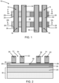
FIG. 1 is a diagrammatic top view illustrating a structure including an array of field-effect transistors at an initial stage of a fabrication method in accordance with embodiments of the invention. -
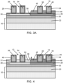
FIG. 2 is a cross-sectional view taken generally along line 2-2 inFIG. 1 . -
FIG. 2A is a cross-sectional view taken generally alongline 2A-2A inFIG. 1 . -
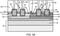
FIGS. 3 ,3A are cross-sectional views of the structure at a fabrication stage subsequent toFIG. 1 . -
FIGS. 4 ,4A are cross-sectional views of the structure at a fabrication stage subsequent toFIGS. 3 ,3A . -
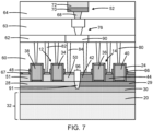
FIGS. 5 ,5A are cross-sectional views of the structure at a fabrication stage subsequent toFIGS. 4 ,4A . -
FIGS. 6 ,6A are cross-sectional views of the structure at a fabrication stage subsequent toFIGS. 5 ,5A . -
FIGS. 7 ,7A are cross-sectional views of a structure in accordance with alternative embodiments of the invention. -
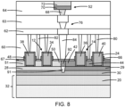
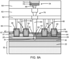
FIGS. 8 ,8A are cross-sectional views of a structure in accordance with alternative embodiments of the invention. -
FIG. 9 is a top view of a structure in accordance with alternative embodiments of the invention. - With reference to
FIGS. 1, 2 ,2A and in accordance with embodiments of the invention, astructure 10 for a resistive random-access memory device includes an array of field-effect transistors semiconductor layers 28,semiconductor layers 29 respectively adjacent to thesemiconductor layers 28, asubstrate 32, and adielectric layer 30 disposed between thesemiconductor layers substrate 32. Thesemiconductor layers 28 may be comprised of a semiconductor material, such as single-crystal silicon, and thesemiconductor layers 29 may be comprised of a different semiconductor material, such as single-crystal silicon-germanium. In an embodiment, thesemiconductor layers 29 may be formed by a condensation process that modifies a section of single-crystal silicon disposed on thedielectric layer 30 by diffusing germanium from a deposited layer of silicon-germanium into the section of single-crystal silicon. Thesemiconductor layer 28 and thesemiconductor layer 29 in each pair may abut or adjoin along aninterface 56, and thesemiconductor layers semiconductor layers respective interface 56. - The
dielectric layer 30 may be comprised of a dielectric material, such as silicon dioxide, that is an electrical insulator. Thesubstrate 32 may be comprised of a semiconductor material, such as silicon, and may be lightly doped with a p-type dopant. Thedielectric layer 30 may have an upper interface with thesemiconductor layers dielectric layer 30 may have a lower interface with thesubstrate 32, and the upper and lower interfaces may be separated by the thickness of thedielectric layer 30. In an embodiment, thesemiconductor layers semiconductor layers dielectric layer 30 may have a thickness in a range of about 10 nm to about 50 nm. - Wells 20, 22 may be formed as doped regions in the
substrate 32. Thewells dielectric layer 30. In an embodiment, thewells well 22. The semiconductor material constituting thewells substrate 32. Thewell 20 is positioned in thesubstrate 32 beneath the pair of thesemiconductor layers effect transistors well 22 is positioned in thesubstrate 32 beneath the pair of thesemiconductor layers effect transistors - The
wells substrate 32 by introducing a dopant by, for example, ion implantation with given implantation conditions. A patterned implantation mask may be formed to define selected areas that are exposed for the implantation of ions. The implantation mask may include a layer of an organic photoresist that is applied and patterned to form openings exposing the selected areas and determining, at least in part, the location and horizontal dimensions of thewells wells wells wells wells - The
well 20 is positioned beneath an active region including thesemiconductor layers effect transistors well 22 is positioned beneath another active region including a different pair of thesemiconductor layers effect transistors isolation layer 25 may electrically isolate the adjacent active regions from each other. In an embodiment, theisolation layer 25 may include shallow trench isolation regions formed by patterning trenches with lithography and etching processes, depositing a dielectric material, such as silicon dioxide, to fill the trenches, and planarizing and/or recessing the dielectric material. - The field-
effect transistor 12 and the field-effect transistor 16 may include a sharedgate electrode 34, and the field-effect transistor 14 and the field-effect transistor 18 may include a sharedgate electrode 36. Thegate electrode 34 extends longitudinally across thesemiconductor layers 28 associated with the field-effect transistor 12 and the field-effect transistor 16, as well as longitudinally across the intervening portion of theisolation layer 25. Thegate electrode 34 is positioned on a portion of eachsemiconductor layer 28. Agate electrode 38 of an adjacent transistor is arranged on thesemiconductor layer 28 adjacent to thegate electrode 34. Thegate electrode 36 extends longitudinally across thesemiconductor layers 29 associated with the field-effect transistor 14 and the field-effect transistor 18, as well as longitudinally across the intervening portion of theisolation layer 25. Thegate electrode 36 is positioned on a portion of eachsemiconductor layer 29 and is located adjacent to thegate electrode 34. Agate electrode 40 of an adjacent transistor is arranged on thesemiconductor layer 29 adjacent to thegate electrode 36. Thegate electrodes gate electrode 38 and thegate electrode 40. In an embodiment, thegate electrode 36 may be arranged directly adjacent to thegate electrode 34 without any intervening gate electrodes. Thegate electrode 34 overlaps with a portion of eachsemiconductor layer 28, thegate electrode 36 overlaps with a portion of eachsemiconductor layer 29, and each pair of the semiconductor layers 28, 29 includes respective portions that are laterally positioned between thegate electrodes isolation layer 25, each of thewells gate electrodes gate electrodes - The
gate electrodes gate electrodes gate electrodes gate electrodes gate dielectric layer 35 comprised of an electrical insulator, such as silicon dioxide, may be disposed between thegate electrodes gate electrodes -
Caps 33, which may be sections of a hardmask used to pattern thegate electrodes gate electrodes caps 33 may be comprised of a dielectric material, such as silicon nitride, that is an electrical insulator. - With reference to
FIGS. 3 ,3A in which like reference numerals refer to like features inFIGS. 2 ,2A and at a subsequent fabrication stage, spacers 24 may be formed on the sidewalls of thegate electrodes protective coating 26 may be formed over thesemiconductor layer 28 andgate electrodes spacers 24 andprotective coating 26 may be comprised of a dielectric material, such as silicon nitride, that is conformally deposited, masked over the semiconductor layers 28 andgate electrodes spacers 24. Portions of the semiconductor layers 29 are exposed adjacent to thespacers 24 and thegate electrodes spacers 24 and thegate electrodes - The field-
effect transistors semiconductor layers semiconductor layers 42 are positioned adjacent to the semiconductor layers 28 andgate electrode 34, which are covered by theprotective coating 26. The raisedsemiconductor layers effect transistors semiconductor layers semiconductor layers 42 may be faceted proximate to therespective interfaces 56 between the semiconductor layers 28 and the semiconductor layers 29. In an embodiment, the field-effect transistors - With reference to
FIGS. 4 ,4A in which like reference numerals refer to like features inFIGS. 3 ,3A and at a subsequent fabrication stage, aprotective coating 46 may be formed over the raisedsemiconductor layers gate electrodes protective coating 46 may be comprised of a dielectric material, such as silicon nitride, that is conformally deposited and patterned by lithography and etching processes. The protective coating 26 (FIGS. 3 ,3A ) may be anisotropically etched to form spacers 48 on the sidewalls of thegate electrodes gate electrodes spacers 48. Other portions of the semiconductor layers 28 are overlapped by thegate electrodes spacers 48. - The field-
effect transistors semiconductor layers semiconductor layers 50 are positioned adjacent to the semiconductor layers 29, thegate electrode 36, and the raised semiconductor layers 42. In an embodiment, the raisedsemiconductor layers 50 may adjoin or abut the raised semiconductor layers 42. In an embodiment, the raisedsemiconductor layers 50 may directly contact the raised semiconductor layers 42. - The raised
semiconductor layers effect transistors semiconductor layers semiconductor layers semiconductor layers semiconductor layer 50 may be beveled proximate to therespective interfaces 56 between the semiconductor layers 28 and the semiconductor layers 29, and may overlap slightly with a portion of the adjacent raisedsemiconductor layer 42. Each pair of the raised semiconductors layers 50 and the raisedsemiconductor layers 42 may abut or adjoin along aninterface 58. - In an embodiment, the field-
effect transistors effect transistors effect transistor 12 and the field-effect transistor 14 may have abutting n-type and p-type source/drain regions in the form of, respectively, abutted raisedsemiconductor layers effect transistor 16 and the field-effect transistor 18 may also have abutting n-type and p-type source/drain regions in the form of, respectively, abutting raisedsemiconductor layers - The well 20 extends beneath the field-
effect transistor 12 and the field-effect transistor 16. A bias can be applied to the well 20 to simultaneously forward bias one of the field-effect transistors (e.g., field-effect transistor 12) and reverse bias the other of the field-effect transistors (e.g., field-effect transistor 16). The well 22 extends beneath the field-effect transistor 14 and the field-effect transistor 18. A bias can be applied to the well 22 to simultaneously forward bias one of the field-effect transistors (e.g., field-effect transistor 14) and reverse bias the other of the field-effect transistors (e.g., field-effect transistor 18). In each instance, the reverse-biasing and forward-biasing are accomplished using the same well, which differs from conventional back-biasing arrangements that rely on distinct wells of different conductivity types to apply a reverse bias and a forward bias to field-effect transistors of complementary types. - With reference to
FIGS. 5 ,5A in which like reference numerals refer to like features inFIGS. 4 ,4A and at a subsequent fabrication stage, spacers 66 may be formed on the sidewalls of thegate electrodes gate electrodes spacers 66 may be formed by depositing a layer comprised of a dielectric material, such as silicon nitride, and etching the deposited layer with an anisotropic etching process. - Silicide layers 67 may be formed on the
gate electrodes gate electrodes semiconductor layers semiconductor layers semiconductor layer 50 may be fully converted to silicide. - The
silicide layer 67 that overlaps with the raisedsemiconductor layer 42 and the raisedsemiconductor layer 50 of the field-effect transistors effect transistors semiconductor layer 42 with the raisedsemiconductor layer 50. Similarly, thesilicide layer 67 that overlaps with the raisedsemiconductor layer 42 and the raisedsemiconductor layer 50 of the field-effect transistors effect transistors semiconductor layer 42 with the raisedsemiconductor layer 50. Each of thesesilicide layers 67 overlaps with one of the interfaces 58 (FIGS. 4 ,4A ). - A
dielectric layer 60 may be formed over the field-effect transistors Gate contacts 80 may be formed in thedielectric layer 60 that are physically and electrically connected to the silicide layers 67 on thegate electrodes drain contacts 82 may be formed in thedielectric layer 60 that are physically and electrically connected to the silicide layers 67 on the raisedsemiconductor layers 44 and the raised semiconductor layers 51. Source/drain contacts 84 may be formed in thedielectric layer 60 that are connected to physically and electrically connected to the silicide layers 67 on the different pairs of abutting raisedsemiconductor layers 42 and raised semiconductor layers 50. One of thespacers 66 may be embedded inside each of the source/drain contacts 84. Each source/drain contact 84 may be located over one of the interfaces 58 (FIGS. 4 ,4A ) between the semiconductor layers 28 and the semiconductor layers 29. Thecontacts dielectric layer 60 may be comprised of a dielectric material, such as silicon dioxide, that is an electrical insulator. - With reference to
FIG. 6 ,6A in which like reference numerals refer to like features inFIGS. 5 ,5A and at a subsequent fabrication stage, an interconnect structure may be formed over the field-effect transistors dielectric layers dielectric layer 60 andcontacts -
Resistive memory elements resistive memory element 52 may be coupled to the field-effect transistors resistive memory element 54 may be coupled to the field-effect transistors effect transistors resistive memory element 52, and the field-effect transistors resistive memory element 54. Thegate electrodes semiconductor layer 44 and the raisedsemiconductor layer 51 of each transistor pair may be connected to bit lines of the resistive random-access memory device. The bit lines may be connected by a bus to peripheral circuits that include, for example, bit line drivers, a multiplexer, and a sense amplifier. - Each of the
resistive memory elements bottom electrode 68, atop electrode 72, and aswitching layer 70 positioned between thebottom electrode 68 and thetop electrode 72. Thebottom electrodes 68 may define respective cathodes of theresistive memory elements top electrodes 72 may define respective anodes of theresistive memory elements bottom electrode 68 comprised of a metal, such as tantalum, titanium nitride, tantalum nitride, or a combination thereof. Eachswitching layer 70 may be comprised of a metal oxide, such as hafnium oxide, magnesium oxide, tantalum oxide, titanium oxide, or aluminum oxide, or a dielectric material, such as silicon nitride or silicon dioxide. Eachtop electrode 72 may be comprised of a metal, such as tungsten, titanium nitride, tantalum nitride, or platinum. The interconnect structure may includevertical interconnections 76 defined by a stack of via plugs and metal features that physically and electrically connect one of the source/drain contacts 84 and the abutted raised semiconductors layers 42, 50 of the field-effect transistors bottom electrode 68 of theresistive memory element 52, and one of the source/drain contacts 84 and the abutted raised semiconductors layers 42, 50 of the field-effect transistors bottom electrode 68 of theresistive memory element 54. - The
structure 10 for the resistive random-access memory device may be expanded to include additional field-effect transistors and additional resistive memory elements. In that regard, the expanded array may include additional wells arranged adjacent to thewells gate electrodes resistive memory elements - The field-
effect transistors effect transistors resistive memory elements gate electrodes resistive memory elements - With reference to
FIGS. 7 ,7A and in accordance with alternative embodiments of the invention, the semiconductor layers 28, 50 and the semiconductor layers 29, 42 may be formed without abutment of the respective side edge portions. As a result, agap 96 may exist between the adjacent side edge portions of the semiconductor layers 28, 50 and the adjacent side edge portions of the semiconductor layers 29, 42. Anisolation region 91 may extend through the semiconductor layers 28, 29 to provide a separation creating thegap 96. - A
local interconnect 90 may be formed as a metal feature in the interconnect structure and may be configured to bridge across thegap 96. Eachlocal interconnect 90 may be physically and electrically connected by the source/drain contacts 84 individually to each adjacent pair of the raisedsemiconductor layers local interconnect 90 may permit the elimination of thedielectric layer 30 between the semiconductor layers 28, 29 and thesubstrate 32 such that the field-effect transistors substrate 32. - With reference to
FIGS. 8 ,8A and in accordance with alternative embodiments of the invention, asemiconductor layer 92 may be formed over theisolation region 91 to bridge the gap 96 (FIGS. 7 ,7A ) and, thereby, physically and electrically connect each pair of the raisedsemiconductor layers semiconductor layer 92 may be formed by an epitaxial growth process. Thesilicide layer 67 may include a portion formed on thesemiconductor layer 92, as well as a portion formed on the raisedsemiconductor layer 42 and a portion formed on the raisedsemiconductor layer 50. - With reference to
FIG. 9 and in accordance with alternative embodiments of the invention, the well 20 may be positioned beneath the active region including the pair of semiconductor layers 28, 29 belonging to the field-effect transistors effect transistors effect transistors 12, 14) and reverse bias the field-effect transistors (e.g., field-effect transistor 16, 18). - The methods as described above are used in the fabrication of integrated circuit chips. The resulting integrated circuit chips can be distributed by the fabricator in raw wafer form (e.g., as a single wafer that has multiple unpackaged chips), as a bare die, or in a packaged form. The chip may be integrated with other chips, discrete circuit elements, and/or other signal processing devices as part of either an intermediate product or an end product. The end product can be any product that includes integrated circuit chips, such as computer products having a central processor or smartphones.
- References herein to terms modified by language of approximation, such as "about", "approximately", and "substantially", are not to be limited to the precise value specified. The language of approximation may correspond to the precision of an instrument used to measure the value and, unless otherwise dependent on the precision of the instrument, may indicate a range of +/- 10% of the stated value(s).
- References herein to terms such as "vertical", "horizontal", etc. are made by way of example, and not by way of limitation, to establish a frame of reference. The term "horizontal" as used herein is defined as a plane parallel to a conventional plane of a semiconductor substrate, regardless of its actual three-dimensional spatial orientation. Furthermore, the term horizontal is can be considered as horizontal to a main surface of any layer formed over the substrate, the main surface of any layer being parallel to the main surface of the substrate. The terms "vertical" and "normal" refer to a direction in the frame of reference perpendicular to the horizontal, as just defined. The term "lateral" refers to a direction in the frame of reference within the horizontal plane.
- A feature "connected" or "coupled" to or with another feature may be directly connected or coupled to or with the other feature or, instead, one or more intervening features may be present. A feature may be "directly connected" or "directly coupled" to or with another feature if intervening features are absent. A feature may be "indirectly connected" or "indirectly coupled" to or with another feature if at least one intervening feature is present. A feature "on" or "contacting" another feature may be directly on or in direct contact with the other feature or, instead, one or more intervening features may be present. A feature may be "directly on" or in "direct contact" with another feature if intervening features are absent. A feature may be "indirectly on" or in "indirect contact" with another feature if at least one intervening feature is present. Different features may "overlap" if a feature extends over, and covers a part of, another feature.
- The descriptions of the various embodiments of the present invention have been presented for purposes of illustration but are not intended to be exhaustive or limited to the embodiments disclosed. Many modifications and variations will be apparent to those of ordinary skill in the art without departing from the scope and spirit of the described embodiments. The terminology used herein was chosen to best explain the principles of the embodiments, the practical application or technical improvement over technologies found in the marketplace, or to enable others of ordinary skill in the art to understand the embodiments disclosed herein.
- In summary, the following embodiments are explicitly disclosed.
- A structure comprising:
- a substrate;
- a dielectric layer on the substrate;
- a first field-effect transistor including a first semiconductor layer over the dielectric layer and a first gate electrode; and
- a second field-effect transistor including a second semiconductor layer over the dielectric layer and a second gate electrode adjacent to the first gate electrode, the second semiconductor layer connected to the first semiconductor layer,
- wherein the first semiconductor layer and the second semiconductor layer are positioned between the first gate electrode and the second gate electrode.
- The structure of embodiment 1, further comprising:
a well in the substrate beneath the first field-effect transistor and the second field-effect transistor. - The structure of
embodiment 2, wherein the first semiconductor layer has p-type conductivity, the second semiconductor layer has n-type conductivity, and the well has p-type conductivity. Embodiment 4:
The structure ofembodiment 2 or 3, wherein the first semiconductor layer has p-type conductivity, the second semiconductor layer has n-type conductivity, and the well has n-type conductivity. - The structure of one of
embodiments 2 to 4 wherein the dielectric layer is positioned between the well and the first semiconductor layer and between the well and the second semiconductor layer. Embodiment 6:
The structure of one of embodiments 1 to 5, wherein the second semiconductor layer adjoins the first semiconductor layer along an interface. - The structure of embodiment 6, further comprising:
a silicide layer on the first semiconductor layer and the second semiconductor layer, the silicide layer extending across the interface. - The structure of embodiment 7, further comprising:
a memory element connected by the silicide layer to the first semiconductor layer and the second semiconductor layer. - The structure of one of embodiments 1 to 8, wherein the second semiconductor layer is spaced from the first semiconductor layer by a gap, and further comprising:
a third semiconductor layer extending across the gap from the first semiconductor layer to the second semiconductor layer. - The structure of embodiment 9, further comprising:
a memory element connected to the third semiconductor layer. - The structure of one of embodiments 1 to 10, further comprising:
an interconnect structure over the first field-effect transistor and the second field-effect transistor, the interconnect structure including a metal feature, a first contact connecting the first semiconductor layer to the metal feature, and a second contact connecting the second semiconductor layer to the metal feature. - The structure of embodiment 11 (without a combination with embodiment 8 or 10), further comprising:
a memory element connected to the metal feature. - The structure of one of embodiments 1 to 12 or of embodiments 1 to 7 and 9 and 11, further comprising:
a memory element connected to the first semiconductor layer and the second semiconductor layer. - The structure of embodiment 13 (without a combination with embodiment 11), further comprising:
- an interconnect structure over the first field-effect transistor and the second field-effect transistor, the interconnect structure including a plurality of dielectric layers in a layer stack,
- wherein the memory element is positioned in the interconnect structure.
- The structure of
embodiment 13 or 14, wherein the memory element includes a first electrode connected to the first semiconductor layer and the second semiconductor layer, a second electrode, and a switching layer positioned between the first electrode and the second electrode. Embodiment 16:
The structure of one of embodiments 1 to 15 (without a combination with embodiment 9 and/or 10), wherein the first field-effect transistor includes a third semiconductor layer between the first semiconductor layer and the dielectric layer, and the second field-effect transistor includes a fourth semiconductor layer between the second semiconductor layer and the dielectric layer. - The structure of
embodiment 16, wherein the third semiconductor layer comprises single-crystal silicon-germanium, and the fourth semiconductor layer comprises single-crystal silicon. - The structure of
embodiment 16 or 17, wherein the first semiconductor layer is positioned on a first portion of the third semiconductor layer, and the second semiconductor layer is positioned on a first portion of the fourth semiconductor layer. - The structure of one of
embodiments 16 to 18, wherein the first gate electrode overlaps with a second portion of the third semiconductor layer, and the second gate electrode overlaps with a second portion of the fourth semiconductor layer. - A structure comprising:
- a substrate;
- a dielectric layer on the substrate;
- a first field-effect transistor including a first semiconductor layer over the dielectric layer and a first gate electrode; and
- a second field-effect transistor including a second semiconductor layer over the dielectric layer and a second gate electrode adjacent to the first gate electrode, the second semiconductor layer connected to the first semiconductor layer,
- wherein the first semiconductor layer and the second semiconductor layer are positioned between the first gate electrode and the second gate electrode.
- The structure of embodiment 1, further comprising:
a well in the substrate beneath the first field-effect transistor and the second field-effect transistor. - The structure of embodiment 21, wherein the first semiconductor layer has p-type conductivity, the second semiconductor layer has n-type conductivity, and the well has one of p-type conductivity and n-type conductivity.
- The structure of
embodiment 21 or 22, wherein the dielectric layer is positioned between the well and the first semiconductor layer and between the well and the second semiconductor layer. Embodiment 24:
The structure of one ofembodiments 20 to 23, wherein the second semiconductor layer adjoins the first semiconductor layer along an interface. - The structure of
embodiment 24, further comprising at least one of: - a silicide layer on the first semiconductor layer and the second semiconductor layer, the silicide layer extending across the interface, and
- a first memory element connected by the silicide layer to the first semiconductor layer and the second semiconductor layer.
- The structure of one of
embodiments 20 to 25, wherein the second semiconductor layer is spaced from the first semiconductor layer by a gap, and further comprising: - a third semiconductor layer extending across the gap from the first semiconductor layer to the second semiconductor layer, and
- the structure preferably further comprising a memory element connected to the third semiconductor layer.
- The structure of one of
embodiments 20 to 26, further comprising: - a first interconnect structure over the first field-effect transistor and the second field-effect transistor, the first interconnect structure including a metal feature, a first contact connecting the first semiconductor layer to the metal feature, and a second contact connecting the second semiconductor layer to the metal feature,
- wherein the structure preferably further comprises a second memory element connected to the metal feature.
- The structure of one of
embodiments 20 to 27, further comprising: - a memory element connected to the first semiconductor layer and the second semiconductor layer,
- wherein the second memory element preferably includes a first electrode connected to the first semiconductor layer and the second semiconductor layer, a second electrode, and a switching layer positioned between the first electrode and the second electrode.
- The structure of
embodiment 28, further comprising: - a second interconnect structure over the first field-effect transistor and the second field-effect transistor, the second interconnect structure including a plurality of dielectric layers in a layer stack,
- wherein the memory element is positioned in the second interconnect structure.
- The structure of one of
embodiments 20 to 29, wherein the first field-effect transistor includes a fourth semiconductor layer between the first semiconductor layer and the dielectric layer, and the second field-effect transistor includes a fifth semiconductor layer between the second semiconductor layer and the dielectric layer. - The structure of
embodiment 30 wherein the fourth semiconductor layer comprises single-crystal silicon-germanium, and the fifth semiconductor layer comprises single-crystal silicon. - The structure of
embodiment 30 or 31, wherein the first semiconductor layer is positioned on a first portion of the fourth semiconductor layer, and the second semiconductor layer is positioned on a first portion of the fifth semiconductor layer. - The structure of one of
embodiments 30 to 32, wherein the first gate electrode overlaps with a second portion of the fourth semiconductor layer, and the second gate electrode overlaps with a second portion of the fifth semiconductor layer. - A method comprising:
- forming a first field-effect transistor including a first semiconductor layer over a dielectric layer and a first gate electrode, wherein the dielectric layer is positioned on a substrate; and
- forming a second field-effect transistor including a second semiconductor layer over the dielectric layer and a second gate electrode adjacent to the first gate electrode, wherein the second semiconductor layer is connected to the first semiconductor layer, and the first semiconductor layer and the second semiconductor layer are positioned between the first gate electrode and the second gate electrode.
- The method of
embodiment 34, wherein the structure of one of embodiments 1 to 33 is formed. - At least in the embodiments above, the term "include" and its variants may be interpreted as meaning that an embodiment includes stated features, while not necessarily excluding the presence of other features that are not explicitly stated.
Claims (15)
- A structure comprising:a substrate;a dielectric layer on the substrate;a first field-effect transistor including a first semiconductor layer over the dielectric layer and a first gate electrode; anda second field-effect transistor including a second semiconductor layer over the dielectric layer and a second gate electrode adjacent to the first gate electrode, the second semiconductor layer connected to the first semiconductor layer,wherein the first semiconductor layer and the second semiconductor layer are positioned between the first gate electrode and the second gate electrode.
- The structure of claim 1, further comprising:
a well in the substrate beneath the first field-effect transistor and the second field-effect transistor. - The structure of claim 2, wherein the first semiconductor layer has p-type conductivity, the second semiconductor layer has n-type conductivity, and the well has one of p-type conductivity and n-type conductivity.
- The structure of claim 2 or 3, wherein the dielectric layer is positioned between the well and the first semiconductor layer and between the well and the second semiconductor layer.
- The structure of one of claims 1 to 4, wherein the second semiconductor layer adjoins the first semiconductor layer along an interface.
- The structure of claim 5, further comprising at least one of:a silicide layer on the first semiconductor layer and the second semiconductor layer, the silicide layer extending across the interface, anda first memory element connected by the silicide layer to the first semiconductor layer and the second semiconductor layer.
- The structure of one of claims 1 to 6, wherein the second semiconductor layer is spaced from the first semiconductor layer by a gap, and further comprising:a third semiconductor layer extending across the gap from the first semiconductor layer to the second semiconductor layer, andthe structure preferably further comprising a memory element connected to the third semiconductor layer.
- The structure of one of claims 1 to 7, further comprising:a first interconnect structure over the first field-effect transistor and the second field-effect transistor, the first interconnect structure including a metal feature, a first contact connecting the first semiconductor layer to the metal feature, and a second contact connecting the second semiconductor layer to the metal feature,wherein the structure preferably further comprises a second memory element connected to the metal feature.
- The structure of one of claims 1 to 8, further comprising:a memory element connected to the first semiconductor layer and the second semiconductor layer,wherein the second memory element preferably includes a first electrode connected to the first semiconductor layer and the second semiconductor layer, a second electrode, and a switching layer positioned between the first electrode and the second electrode.
- The structure of claim 9, further comprising:a second interconnect structure over the first field-effect transistor and the second field-effect transistor, the second interconnect structure including a plurality of dielectric layers in a layer stack,wherein the memory element is positioned in the second interconnect structure.
- The structure of one of claims 1 to 10, wherein the first field-effect transistor includes a fourth semiconductor layer between the first semiconductor layer and the dielectric layer, and the second field-effect transistor includes a fifth semiconductor layer between the second semiconductor layer and the dielectric layer.
- The structure of claim 11, wherein the fourth semiconductor layer comprises single-crystal silicon-germanium, and the fifth semiconductor layer comprises single-crystal silicon.
- The structure of claim 11 or 12, wherein the first semiconductor layer is positioned on a first portion of the fourth semiconductor layer, and the second semiconductor layer is positioned on a first portion of the fifth semiconductor layer.
- The structure of one of claims 11 to 13, wherein the first gate electrode overlaps with a second portion of the fourth semiconductor layer, and the second gate electrode overlaps with a second portion of the fifth semiconductor layer.
- A method comprising:forming a first field-effect transistor including a first semiconductor layer over a dielectric layer and a first gate electrode, wherein the dielectric layer is positioned on a substrate; andforming a second field-effect transistor including a second semiconductor layer over the dielectric layer and a second gate electrode adjacent to the first gate electrode, wherein the second semiconductor layer is connected to the first semiconductor layer, and the first semiconductor layer and the second semiconductor layer are positioned between the first gate electrode and the second gate electrode.
Applications Claiming Priority (1)
| Application Number | Priority Date | Filing Date | Title |
|---|---|---|---|
| US18/080,017 US12532534B2 (en) | 2022-12-13 | 2022-12-13 | Transistor arrays with controllable gate voltage |
Publications (3)
| Publication Number | Publication Date |
|---|---|
| EP4387410A1 true EP4387410A1 (en) | 2024-06-19 |
| EP4387410C0 EP4387410C0 (en) | 2025-10-22 |
| EP4387410B1 EP4387410B1 (en) | 2025-10-22 |
Family
ID=88092961
Family Applications (1)
| Application Number | Title | Priority Date | Filing Date |
|---|---|---|---|
| EP23197413.0A Active EP4387410B1 (en) | 2022-12-13 | 2023-09-14 | Transistor arrays with controllable gate voltage |
Country Status (3)
| Country | Link |
|---|---|
| US (1) | US12532534B2 (en) |
| EP (1) | EP4387410B1 (en) |
| CN (1) | CN118201371A (en) |
Families Citing this family (1)
| Publication number | Priority date | Publication date | Assignee | Title |
|---|---|---|---|---|
| US12376315B2 (en) * | 2022-07-18 | 2025-07-29 | Globalfoundries U.S. Inc. | Resistive memory element arrays with shared electrode strips |
Citations (4)
| Publication number | Priority date | Publication date | Assignee | Title |
|---|---|---|---|---|
| US20090194760A1 (en) * | 2008-02-01 | 2009-08-06 | Sony Corporation | Memory element and display device |
| US20190363135A1 (en) * | 2016-09-29 | 2019-11-28 | Intel Corporation | Resistive random access memory cell |
| US20220020757A1 (en) * | 2018-12-18 | 2022-01-20 | Sony Group Corporation | Semiconductor storage device and neural network device |
| EP4312479A1 (en) * | 2022-07-18 | 2024-01-31 | GlobalFoundries U.S. Inc. | Resistive memory element arrays with shared electrode strips |
Family Cites Families (11)
| Publication number | Priority date | Publication date | Assignee | Title |
|---|---|---|---|---|
| US7663237B2 (en) | 2005-12-27 | 2010-02-16 | Taiwan Semiconductor Manufacturing Company, Ltd. | Butted contact structure |
| TWI365489B (en) | 2006-12-20 | 2012-06-01 | Richtek Technology Corp | Semiconductor process for butting contact and semiconductor circuit device having a butting contact |
| US8299453B2 (en) * | 2009-03-03 | 2012-10-30 | International Business Machines Corporation | CMOS transistors with silicon germanium channel and dual embedded stressors |
| US8395191B2 (en) * | 2009-10-12 | 2013-03-12 | Monolithic 3D Inc. | Semiconductor device and structure |
| US8592325B2 (en) * | 2010-01-11 | 2013-11-26 | International Business Machines Corporation | Insulating layers on different semiconductor materials |
| US8237197B2 (en) * | 2010-07-07 | 2012-08-07 | International Business Machines Corporation | Asymmetric channel MOSFET |
| US8741725B2 (en) | 2010-11-10 | 2014-06-03 | International Business Machines Corporation | Butted SOI junction isolation structures and devices and method of fabrication |
| US9006064B2 (en) * | 2013-03-11 | 2015-04-14 | International Business Machines Corporation | Multi-plasma nitridation process for a gate dielectric |
| US9472272B2 (en) | 2015-02-22 | 2016-10-18 | Adesto Technologies Corporation | Resistive switching memory with cell access by analog signal controlled transmission gate |
| US11088022B2 (en) * | 2018-09-27 | 2021-08-10 | Taiwan Semiconductor Manufacturing Co., Ltd. | Different isolation liners for different type FinFETs and associated isolation feature fabrication |
| US12501600B2 (en) * | 2021-10-04 | 2025-12-16 | Invention And Collaboration Laboratory Pte. Ltd. | SRAM cell structure |
-
2022
- 2022-12-13 US US18/080,017 patent/US12532534B2/en active Active
-
2023
- 2023-09-14 EP EP23197413.0A patent/EP4387410B1/en active Active
- 2023-11-09 CN CN202311487624.6A patent/CN118201371A/en active Pending
Patent Citations (4)
| Publication number | Priority date | Publication date | Assignee | Title |
|---|---|---|---|---|
| US20090194760A1 (en) * | 2008-02-01 | 2009-08-06 | Sony Corporation | Memory element and display device |
| US20190363135A1 (en) * | 2016-09-29 | 2019-11-28 | Intel Corporation | Resistive random access memory cell |
| US20220020757A1 (en) * | 2018-12-18 | 2022-01-20 | Sony Group Corporation | Semiconductor storage device and neural network device |
| EP4312479A1 (en) * | 2022-07-18 | 2024-01-31 | GlobalFoundries U.S. Inc. | Resistive memory element arrays with shared electrode strips |
Also Published As
| Publication number | Publication date |
|---|---|
| US20240194535A1 (en) | 2024-06-13 |
| US12532534B2 (en) | 2026-01-20 |
| EP4387410C0 (en) | 2025-10-22 |
| CN118201371A (en) | 2024-06-14 |
| EP4387410B1 (en) | 2025-10-22 |
Similar Documents
| Publication | Publication Date | Title |
|---|---|---|
| US6194301B1 (en) | Method of fabricating an integrated circuit of logic and memory using damascene gate structure | |
| US11527493B2 (en) | Method for preparing semiconductor device structure with air gap structure | |
| US20080283910A1 (en) | Integrated circuit and method of forming an integrated circuit | |
| US11967626B2 (en) | Field effect transistors with gate fins and method of making the same | |
| KR20120108066A (en) | Methods of providing electrical isolation and semiconductor structures including same | |
| US7390730B2 (en) | Method of fabricating a body capacitor for SOI memory | |
| US12015084B2 (en) | Field effect transistors with gate fins and method of making the same | |
| US12426278B2 (en) | Resistive memory elements accessed by bipolar junction transistors | |
| US8227301B2 (en) | Semiconductor device structures with floating body charge storage and methods for forming such semiconductor device structures | |
| EP4373237B1 (en) | Bipolar junction transistor arrays | |
| EP4387410B1 (en) | Transistor arrays with controllable gate voltage | |
| KR20240009798A (en) | Semiconductor device | |
| EP4312479B1 (en) | Resistive memory element arrays with shared electrode strips and a method | |
| US5374572A (en) | Method of forming a transistor having an offset channel section | |
| KR100404682B1 (en) | Method for manufacturing a silicide layer of flat cell memory device | |
| CN117855271A (en) | Ferroelectric field effect transistor with hybrid well | |
| US12471294B2 (en) | Array arrangements of vertical bipolar junction transistors | |
| US12266702B2 (en) | Flash memory devices with thickened source/drain silicide | |
| US20250267861A1 (en) | Flash memory cell arrays with a control gate strap | |
| US20240268241A1 (en) | Layer stacks for a resistive memory element | |
| JPH1050950A (en) | Method for manufacturing semiconductor integrated circuit device | |
| EP4739022A1 (en) | Semiconductor device including active portion and bit line |
Legal Events
| Date | Code | Title | Description |
|---|---|---|---|
| PUAI | Public reference made under article 153(3) epc to a published international application that has entered the european phase |
Free format text: ORIGINAL CODE: 0009012 |
|
| STAA | Information on the status of an ep patent application or granted ep patent |
Free format text: STATUS: REQUEST FOR EXAMINATION WAS MADE |
|
| 17P | Request for examination filed |
Effective date: 20230914 |
|
| AK | Designated contracting states |
Kind code of ref document: A1 Designated state(s): AL AT BE BG CH CY CZ DE DK EE ES FI FR GB GR HR HU IE IS IT LI LT LU LV MC ME MK MT NL NO PL PT RO RS SE SI SK SM TR |
|
| GRAP | Despatch of communication of intention to grant a patent |
Free format text: ORIGINAL CODE: EPIDOSNIGR1 |
|
| STAA | Information on the status of an ep patent application or granted ep patent |
Free format text: STATUS: GRANT OF PATENT IS INTENDED |
|
| RIC1 | Information provided on ipc code assigned before grant |
Ipc: G11C 13/00 20060101ALI20250424BHEP Ipc: H10D 86/60 20250101ALI20250424BHEP Ipc: H10D 86/40 20250101ALI20250424BHEP Ipc: H10D 86/01 20250101ALI20250424BHEP Ipc: H10D 86/00 20250101ALI20250424BHEP Ipc: G11C 11/16 20060101ALI20250424BHEP Ipc: H10N 70/20 20230101ALI20250424BHEP Ipc: H10B 63/00 20230101AFI20250424BHEP |
|
| INTG | Intention to grant announced |
Effective date: 20250523 |
|
| RIN1 | Information on inventor provided before grant (corrected) |
Inventor name: PAUL, BIPUL C. Inventor name: PENG, JIANWEI Inventor name: DERRICKSON, ALEXANDER Inventor name: REN, HONGRU Inventor name: JAIN, NAVNEET Inventor name: GOPINATH, VENKATESH P. |
|
| GRAS | Grant fee paid |
Free format text: ORIGINAL CODE: EPIDOSNIGR3 |
|
| GRAA | (expected) grant |
Free format text: ORIGINAL CODE: 0009210 |
|
| STAA | Information on the status of an ep patent application or granted ep patent |
Free format text: STATUS: THE PATENT HAS BEEN GRANTED |
|
| AK | Designated contracting states |
Kind code of ref document: B1 Designated state(s): AL AT BE BG CH CY CZ DE DK EE ES FI FR GB GR HR HU IE IS IT LI LT LU LV MC ME MK MT NL NO PL PT RO RS SE SI SK SM TR |
|
| REG | Reference to a national code |
Ref country code: CH Ref legal event code: F10 Free format text: ST27 STATUS EVENT CODE: U-0-0-F10-F00 (AS PROVIDED BY THE NATIONAL OFFICE) Effective date: 20251022 Ref country code: GB Ref legal event code: FG4D |
|
| REG | Reference to a national code |
Ref country code: DE Ref legal event code: R096 Ref document number: 602023007723 Country of ref document: DE |
|
| REG | Reference to a national code |
Ref country code: IE Ref legal event code: FG4D |
|
| U01 | Request for unitary effect filed |
Effective date: 20251031 |
|
| U07 | Unitary effect registered |
Designated state(s): AT BE BG DE DK EE FI FR IT LT LU LV MT NL PT RO SE SI Effective date: 20251110 |
|
| PG25 | Lapsed in a contracting state [announced via postgrant information from national office to epo] |
Ref country code: ES Free format text: LAPSE BECAUSE OF FAILURE TO SUBMIT A TRANSLATION OF THE DESCRIPTION OR TO PAY THE FEE WITHIN THE PRESCRIBED TIME-LIMIT Effective date: 20251022 |
|
| PG25 | Lapsed in a contracting state [announced via postgrant information from national office to epo] |
Ref country code: NO Free format text: LAPSE BECAUSE OF FAILURE TO SUBMIT A TRANSLATION OF THE DESCRIPTION OR TO PAY THE FEE WITHIN THE PRESCRIBED TIME-LIMIT Effective date: 20260122 |
|
| PG25 | Lapsed in a contracting state [announced via postgrant information from national office to epo] |
Ref country code: HR Free format text: LAPSE BECAUSE OF FAILURE TO SUBMIT A TRANSLATION OF THE DESCRIPTION OR TO PAY THE FEE WITHIN THE PRESCRIBED TIME-LIMIT Effective date: 20251022 |
|
| PG25 | Lapsed in a contracting state [announced via postgrant information from national office to epo] |
Ref country code: RS Free format text: LAPSE BECAUSE OF FAILURE TO SUBMIT A TRANSLATION OF THE DESCRIPTION OR TO PAY THE FEE WITHIN THE PRESCRIBED TIME-LIMIT Effective date: 20260122 |
|
| PG25 | Lapsed in a contracting state [announced via postgrant information from national office to epo] |
Ref country code: IS Free format text: LAPSE BECAUSE OF FAILURE TO SUBMIT A TRANSLATION OF THE DESCRIPTION OR TO PAY THE FEE WITHIN THE PRESCRIBED TIME-LIMIT Effective date: 20260222 |
|
| PG25 | Lapsed in a contracting state [announced via postgrant information from national office to epo] |
Ref country code: PL Free format text: LAPSE BECAUSE OF FAILURE TO SUBMIT A TRANSLATION OF THE DESCRIPTION OR TO PAY THE FEE WITHIN THE PRESCRIBED TIME-LIMIT Effective date: 20251022 |
|
| PG25 | Lapsed in a contracting state [announced via postgrant information from national office to epo] |
Ref country code: SM Free format text: LAPSE BECAUSE OF FAILURE TO SUBMIT A TRANSLATION OF THE DESCRIPTION OR TO PAY THE FEE WITHIN THE PRESCRIBED TIME-LIMIT Effective date: 20251022 |
|
| PG25 | Lapsed in a contracting state [announced via postgrant information from national office to epo] |
Ref country code: CZ Free format text: LAPSE BECAUSE OF FAILURE TO SUBMIT A TRANSLATION OF THE DESCRIPTION OR TO PAY THE FEE WITHIN THE PRESCRIBED TIME-LIMIT Effective date: 20251022 |
|
| PG25 | Lapsed in a contracting state [announced via postgrant information from national office to epo] |
Ref country code: SK Free format text: LAPSE BECAUSE OF FAILURE TO SUBMIT A TRANSLATION OF THE DESCRIPTION OR TO PAY THE FEE WITHIN THE PRESCRIBED TIME-LIMIT Effective date: 20251022 |