EP4387398A1 - Hysteresis circuit, emergency lighting circuit, and lighting device - Google Patents
Hysteresis circuit, emergency lighting circuit, and lighting device Download PDFInfo
- Publication number
- EP4387398A1 EP4387398A1 EP22857643.5A EP22857643A EP4387398A1 EP 4387398 A1 EP4387398 A1 EP 4387398A1 EP 22857643 A EP22857643 A EP 22857643A EP 4387398 A1 EP4387398 A1 EP 4387398A1
- Authority
- EP
- European Patent Office
- Prior art keywords
- voltage
- resistor
- electrically connected
- sampling
- pin
- Prior art date
- Legal status (The legal status is an assumption and is not a legal conclusion. Google has not performed a legal analysis and makes no representation as to the accuracy of the status listed.)
- Pending
Links
- 238000005070 sampling Methods 0.000 claims abstract description 65
- 230000008878 coupling Effects 0.000 claims abstract description 44
- 238000010168 coupling process Methods 0.000 claims abstract description 44
- 238000005859 coupling reaction Methods 0.000 claims abstract description 44
- 238000002955 isolation Methods 0.000 claims abstract description 34
- 238000001514 detection method Methods 0.000 claims description 33
- 239000003990 capacitor Substances 0.000 claims description 17
- 230000000087 stabilizing effect Effects 0.000 claims description 9
- 230000009471 action Effects 0.000 abstract description 13
- 238000011084 recovery Methods 0.000 abstract description 12
- 230000003247 decreasing effect Effects 0.000 abstract description 2
- 238000005259 measurement Methods 0.000 abstract 1
- 230000007423 decrease Effects 0.000 description 13
- 238000010586 diagram Methods 0.000 description 6
- 238000000034 method Methods 0.000 description 4
- 230000033228 biological regulation Effects 0.000 description 2
- 230000000694 effects Effects 0.000 description 2
- 238000012544 monitoring process Methods 0.000 description 2
- 230000008569 process Effects 0.000 description 2
- 241001621399 Lampris Species 0.000 description 1
- 230000009286 beneficial effect Effects 0.000 description 1
- 238000005516 engineering process Methods 0.000 description 1
- 238000009434 installation Methods 0.000 description 1
- 230000003993 interaction Effects 0.000 description 1
- 238000004519 manufacturing process Methods 0.000 description 1
- 238000012986 modification Methods 0.000 description 1
- 230000004048 modification Effects 0.000 description 1
- 230000000630 rising effect Effects 0.000 description 1
Images


Classifications
-
- H—ELECTRICITY
- H05—ELECTRIC TECHNIQUES NOT OTHERWISE PROVIDED FOR
- H05B—ELECTRIC HEATING; ELECTRIC LIGHT SOURCES NOT OTHERWISE PROVIDED FOR; CIRCUIT ARRANGEMENTS FOR ELECTRIC LIGHT SOURCES, IN GENERAL
- H05B47/00—Circuit arrangements for operating light sources in general, i.e. where the type of light source is not relevant
- H05B47/10—Controlling the light source
- H05B47/105—Controlling the light source in response to determined parameters
- H05B47/14—Controlling the light source in response to determined parameters by determining electrical parameters of the light source
-
- H—ELECTRICITY
- H05—ELECTRIC TECHNIQUES NOT OTHERWISE PROVIDED FOR
- H05B—ELECTRIC HEATING; ELECTRIC LIGHT SOURCES NOT OTHERWISE PROVIDED FOR; CIRCUIT ARRANGEMENTS FOR ELECTRIC LIGHT SOURCES, IN GENERAL
- H05B47/00—Circuit arrangements for operating light sources in general, i.e. where the type of light source is not relevant
- H05B47/10—Controlling the light source
- H05B47/17—Operational modes, e.g. switching from manual to automatic mode or prohibiting specific operations
- H05B47/172—Emergency operational modes
-
- H—ELECTRICITY
- H05—ELECTRIC TECHNIQUES NOT OTHERWISE PROVIDED FOR
- H05B—ELECTRIC HEATING; ELECTRIC LIGHT SOURCES NOT OTHERWISE PROVIDED FOR; CIRCUIT ARRANGEMENTS FOR ELECTRIC LIGHT SOURCES, IN GENERAL
- H05B47/00—Circuit arrangements for operating light sources in general, i.e. where the type of light source is not relevant
- H05B47/10—Controlling the light source
Definitions
- the present application relates to a field of lighting circuit technology, specifically to a hysteresis circuit, an emergency lighting circuit, and a lighting device.
- the emergency lighting is different from ordinary lighting, and the emergency lighting includes three types: backup lighting, evacuation lighting, and safety lighting.
- the emergency lighting is an important safety facility in modern public building and industrial building, and it is closely related to personal safety and building safety. When a building experiences a fire or other disaster, and the power supply is interrupted, the emergency lighting plays an important role in personnel evacuation, fire rescue work, and the continued operation or necessary operation and disposal of important production and work.
- the fire emergency lighting and evacuation indication system includes the power supply of emergency lighting fixtures and evacuation indication fixtures.
- emergency lighting centralized power supply there are the following regulations: when the main power supply voltage of the lamp works at any voltage within the range of 60% -80% of its rated voltage, the status indicator lights and the relays of the emergency lighting centralized power supply should not have multiple switching phenomena. If multiple switching phenomena occur, it will inevitably cause ripple and instability of the main power supply voltage of the lamp.
- the relevant technical personnel proposed a scheme as shown in FIG. 1 to determine the situation of the main power supply voltage of the lamp.
- the ADC sampling value is obtained by using a microcontroller U4, and the following logical judgment is made: determining whether the input voltage Vbus has reached the trigger action voltage point, and when it returns to normal operation, determining whether the input voltage Vbus has reached the reverse recovery voltage point.
- the trigger action voltage point refers to the voltage value corresponding to reaching a preset function (such as triggering an emergency function)
- the reverse recovery voltage point refers to the voltage value corresponding to before restoring to the preset function (such as restoring to normal operation).
- the above scheme has specific limitations, which include: 1) only for non isolated power sources,where the input voltage and the microcontroller are grounded, making the scheme suitable for applications with broad requirements for product safety design; 2) only suitable for circuits with microcontroller control and suitable ADC sampling value detection ports.
- the purpose of the present application is to provide a hysteresis circuit, an emergency lighting circuit, and a lighting device, which aims to detect a sampling voltage associated with the input voltage.
- the sampling voltage is detected to decrease to the trigger action voltage point, the corresponding level of the output signal is controlled to flip until it is detected that the sampling voltage has risen to the reverse recovery voltage point, the corresponding level of the output signal is controlled to flip again, so as to achieve timely and accurate monitoring of the input voltage status, further improving the reliability and safety of the product.
- an embodiment of the present application provides a hysteresis circuit
- the hysteresis circuit includes: a voltage detection module, configured to receive an input voltage and generate a sampling voltage based on the input voltage, and detect the sampling voltage; a solation coupling module, configured to control an output signal of the isolation coupling module based on the sampling voltage; and a voltage adjusting module, configured to adjust the sampling voltage; in a case that the voltage detection module detects that the sampling voltage is less than a first set value, an optocoupler in the isolation coupling module is controlled to be in an isolating state, so that the output signal of the isolation coupling module is a first level signal, and the voltage adjusting module begins to adjust the sampling voltage; in a case that the voltage detection module detects that the sampling voltage is greater than a second set value, the optocoupler is controlled to be in a coupling state, so that the output signal of the isolation coupling module is a second level signal, and the voltage adjusting module stops
- the voltage detection module comprises: a first voltage divider resistor, a second voltage divider resistor, a first capacitor, and a voltage regulator; a first end of the first voltage divider resistor receives the input voltage, and a second end of the first voltage divider resistor is connected to a first end of the second voltage divider resistor to form a first node, the first voltage divider resistor and the second voltage divider resistor are configured to divide the input voltage so that a voltage of the first node is the sampling voltage, the first end of the second voltage divider resistor is electrically connected to a first end of the first capacitor and a first pin of the voltage regulator, and a second end of the second voltage divider resistor is electrically connected to a second end of the first capacitor and a third pin of the voltage regulator, respectively; a first end of the first capacitor is electrically connected to the first pin of the voltage regulator, and the second end of the first capacitor is electrically connected to the third pin of the voltage regulator; a second pin of the voltage regulator is connected to the
- the voltage regulator in a case that the sampling voltage obtained by the first pin of the voltage regulator is less than the first set value, the voltage regulator is in a cut-off state; in a case that the sampling voltage obtained by the first pin of the voltage regulator is greater than the second set value, the voltage regulator is in a conductive state.
- the isolation coupling module further comprises: a fifth resistor and a sixth resistor; a first end of the fifth resistor receives a first side supply voltage, and a second end of the fifth resistor is electrically connected to a positive electrode of a light-emitting diode on a primary side of the optocoupler; a first end of the sixth resistor is connected to a second side supply voltage, and a second end of the sixth resistor is electrically connected to a collector electrode of a triode on a secondary side of the optocoupler; a negative electrode of the light-emitting diode on the primary side of the optocoupler is electrically connected to a second pin of the voltage regulator in the voltage detection module, and an emitter electrode of the triode on the secondary side of the optocoupler is connected to a signal ground.
- the voltage adjusting module comprises: a first voltage stabilizing transistor, a seventh resistor, an eighth resistor, a ninth resistor, and a first switching transistor; a first end of the first voltage stabilizing transistor is electrically connected to a first end of the seventh resistor, and a second end of the first voltage stabilizing transistor is electrically connected to a second end of the fifth resistor in the isolation coupling module; a second end of the seventh resistor is electrically connected to a first end of the eighth resistor and a control end of the first switching transistor, respectively; a first end of the eighth resistor is electrically connected to a control end of the first switching transistor, and a second end of the eighth resistor is electrically connected to a first end of the first switching transistor; a first end of the ninth resistor is electrically connected to a first end of a second voltage divider resistor in the voltage detection module, and a second end of the ninth resistor is electrically connected to a second end of the first switching transistor; a first end of the first switching transistor is respectively
- a second voltage divider resistor in the voltage detection module and a ninth resistor in the voltage adjusting module are variable resistors.
- the first set value is configured to be associated with a resistance value of the second divider resistor; and the second set value is configured to be associated with a resistance value of the ninth resistor.
- a power ground connected to a voltage regulator in the voltage detection module on a primary side of the optocoupler is not in common ground with a signal ground connected to the secondary side of the optocoupler.
- an embodiment of the present application provides an emergency lighting circuit
- the emergency lighting circuit comprises a rectification circuit, configured to convert an input AC power into a DC power to provide the DC power to the hysteresis circuit; the hysteresis circuit in any one of the embodiments of the present application; a control circuit, configured to control an operation of an indicator light or a relay based on the output signal of the isolation coupling module in the hysteresis circuit.
- an embodiment of the present application provides a lighting device, and the lighting device comprises an emergency lighting circuit as described in any one of the embodiments of the present application.
- the hysteresis circuit, the emergency lighting circuit, and the lighting device aim to detect a sampling voltage associated with the input voltage.
- the sampling voltage is detected to decrease to the trigger action voltage point, the corresponding level of the output signal is controlled to flip until it is detected that the sampling voltage has risen to the reverse recovery voltage point, the corresponding level of the control output signal is controlled to flip again, so as to achieve hysteresis design for the input voltage detection, thereby achieving timely and accurate monitoring of input voltage status, and ensuring that emergency lighting circuits work according to specified requirements, and improving product reliability and safety.
- the terms “installation”, “connection”, and “coupling” should be broadly understood, for example, they can be fixed connections, detachable connections, or integrated connections; they can be mechanical connections, electrical connections, or signal connections with each other; they can be direct connection or indirect connection through an intermediate medium, and can be the internal connection of two components or the interaction relationship between two components.
- installation should be broadly understood, for example, they can be fixed connections, detachable connections, or integrated connections; they can be mechanical connections, electrical connections, or signal connections with each other; they can be direct connection or indirect connection through an intermediate medium, and can be the internal connection of two components or the interaction relationship between two components.
- FIG. 2 is a schematic diagram of an architecture of a hysteresis circuit provided by an embodiment of the present application.
- the hysteresis circuit 1000 includes a voltage detection module 110 configured to receive an input voltage Vbus, generate a sampling voltage VA based on the input voltage Vbus, and detect the sampling voltage VA; an isolation coupling module 120 configured to control the output signal Vbus_c of the isolation coupling module 120 based on the sampling voltage; a voltage adjusting module 130 configured to adjust the sampling voltage VA; in a case that the voltage detection module 110 detects that the sampling voltage VA is less than a first set value, the optocoupler U1 in the isolation coupling module 120 is controlled to be in an isolating state, so that the output signal Vbus_c of the isolation coupling module 120 is a first level signal, and the voltage adjusting module 130 starts adjusting the sampling voltage VA; in a case that the voltage detection module 110 detects that the sampling voltage VA is greater than a second set value, the optocoupler U1 is controlled to be in a coupling state
- This design can achieve hysteresis design for input voltage detection, enabling timely and accurate judgment of the status of the input voltage, and also ensuring that the corresponding emergency lighting circuit operates normally according to specified requirements, thereby improving the reliability and safety of the lighting device.
- an embodiment of the present application provides a hysteresis circuit 1000, which includes a voltage detection module 110, an isolation coupling module 120, and a voltage adjusting module 130.
- the voltage detection module 110 may include: a first voltage divider resistor and a second voltage divider resistor, a first capacitor C1, and a voltage regulator U2.
- a first end of the first voltage divider resistor receives the input voltage, and a second end of the first voltage divider resistor is connected to a first end of the second voltage divider resistor to form a first node A.
- the first voltage divider resistor and the second voltage divider resistor are configured to divide the input voltage so that the voltage of the first node A is the sampling voltage.
- the first voltage divider resistor may include a first resistor R1, a second resistor R2, and a third resistor R3, but in other partial embodiments, the first voltage divider resistor may include a plurality of resistors or only one resistor.
- the second voltage divider resistor is the fourth resistor R4 (which will be described below as the fourth resistor). As shown in FIG. 2 , specifically, a first end of the first resistor R1 receives the input voltage Vbus, and a second end of the first resistor R1 is electrically connected to a first end of the second resistor R2.
- a second end of the second resistor R2 is electrically connected to a first end of the third resistor R3, and a second end of the third resistor R3 is electrically connected to a first end of the fourth resistor R4, a first end of the first capacitor C1, and a first pin of the voltage regulator U2, respectively.
- the first end of the fourth resistor R4 is electrically connected to the first end of the first capacitor C1 and the first pin of the voltage regulator U2, respectively.
- a second end of the fourth resistor R4 is electrically connected to a second end of the first capacitor C1 and a third pin of the voltage regulator U2, respectively.
- the first end of the first capacitor C1 is electrically connected to the first pin of the voltage regulator U2, and the second end of the first capacitor C1 is electrically connected to the third pin of the voltage regulator U2.
- a second pin of the voltage regulator U2 is connected to the isolation coupling module 120, and the third pin of the voltage regulator U2 is connected to a power ground.
- the first resistor R1, the second resistor R2, the third resistor R3, and the fourth resistor R4 are sequentially connected in series.
- the first resistor R1 receives the input voltage Vbus.
- the input voltage Vbus may be a DC voltage, which can be obtained through the rectification circuit in the emergency lighting circuit.
- the resistance values of the first resistor R1, the second resistor R2, and the third resistor R3 are the same and different from the resistance value of the fourth resistor R4.
- the fourth resistor R4 and the three resistors mentioned above divide the input voltage to obtain the sampling voltage VA of the first node A. As shown in FIG.
- the voltage of the first node A is the sampling voltage VA, which is the same in the following text.
- the voltage obtained from the first pin of the voltage regulator U2 is the sampling voltage VA.
- the voltage regulator U2 is in a cut-off state; when the sampling voltage obtained by the first pin of the voltage regulator U2 is greater than the second set value, the voltage regulator U2 is in a conductive state. Therefore, the voltage regulator U2 can be regarded as a switching element.
- the first capacitor C1 is connected in parallel with the fourth resistor R4, which is configured to filter the voltage signal received by the first pin of the voltage regulator U2.
- the voltage regulator U2 may adopt a TL43 1M type voltage regulator, with an internal reference voltage of 2.5V. If other models of voltage regulators are used, their internal reference voltage may be different.
- the isolation coupling module 120 includes a fifth resistor R5, a sixth resistor R6, and an optocoupler U1.
- a first end of the fifth resistor R5 receives a first side supply voltage VF, and a second end of the fifth resistor R5 is electrically connected to a positive electrode of a light-emitting diode on a primary side of the optocoupler U1.
- a first end of the sixth resistor R6 is connected to a second side supply voltage VDD, and a second end of the sixth resistor R6 is electrically connected to a collector electrode of a triode on a secondary side of the optocoupler U1.
- a negative electrode of the light-emitting diode on the primary side of the optocoupler U1 is electrically connected to a second pin of the voltage regulator U2 in the voltage detection module 110, and an emitter electrode of the triode on the secondary side of the optocoupler U1 is connected to a signal ground.
- the optocoupler U1 adopts an EL817 type optocoupler, which is not limited to this.
- the triode on the secondary side works normally, causing the optocoupler U1 to be in a coupling state.
- the triode on the secondary side does not work, so that the optocoupler U1 is in an isolating state.
- the first side supply voltage VF received by the first end of the fifth resistor R5 and the second side supply voltage VDD received by the first end of the sixth resistor R6 are both fixed supply voltages.
- the power ground connected to the voltage regulator U2 in the voltage detection module 110 on the primary side of the optocoupler U1 is not in common ground with the signal ground connected to the secondary side of the optocoupler U1.
- the power ground and the signal ground can be grounded together (applicable to non isolated power sources).
- the voltage adjusting module 130 includes: a first voltage stabilizing transistor ZD1, a seventh resistor R7, an eighth resistor R8, a ninth resistor R9, and a first switching transistor Q1.
- a first end of the first voltage stabilizing transistor ZD1 is electrically connected to a first end of the seventh resistor R7, and a second end of the first voltage stabilizing transistor ZD1 is electrically connected to the second end of the fifth resistor R5 in the isolation coupling module 120.
- a second end of the seventh resistor R7 is electrically connected to a first end of the eighth resistor R8 and a control end of the first switching transistor Q1, respectively.
- a first end of the eighth resistor R8 is electrically connected to the control end of the first switching transistor Q1, and a second end of the eighth resistor R8 is electrically connected to a first end of the first switching transistor Q1.
- a first end of the ninth resistor R9 is electrically connected to a first end of the fourth resistor R4 in the voltage detection module 110, and a second end of the ninth resistor R9 is electrically connected to a second end of the first switching transistor Q1.
- the first end of the first switching transistor Q1 is respectively connected to a second end of the fourth resistor R4 in the voltage detection module 110 and a power ground.
- the ninth resistor R9 is connected in series with the first switching transistor Q1, and then connected in parallel with the fourth resistor R4.
- the first switching transistor Q1 When the first switching transistor Q1 is in a conductive state, its conducting resistance is connected in series with the ninth resistor R9, and then in parallel with the fourth resistor R4.
- the first switching transistor Q1 When the first switching transistor Q1 is in the cut-off state, its resistance value is very high, after being connected in series with the ninth resistor R9, the effect on the resistance value of the fourth resistor R4 connected in parallel can be ignored.
- the ground resistance of the first pin of the voltage regulator U2 is an equivalent resistance corresponding to the parallel connection of the fourth resistor R4, the ninth resistor R9, and the conduction resistance of the first switching transistor Q1.
- the resistance value of the first switching transistor Q1 is very large. Therefore, the ground resistance of the first pin of the voltage regulator U2 is the fourth resistor R4. In this way, when the first switching transistor Q1 is turned on, the ground resistance of the first pin of the voltage regulator U2 is smaller than the ground resistance of the first pin of the voltage regulator U2 when the first switching transistor Q1 is turned off.
- the fourth resistor R4 in the voltage detection module 110 and the ninth resistor R9 in the voltage adjusting module 130 are variable resistors.
- the sampling voltage VA increases.
- the sampling voltage VA decreases.
- the first switching transistor Q1 is in a conductive state
- the hysteresis voltage decreases.
- the resistance value of the ninth resistor R9 decreases, the hysteresis voltage increases.
- the first set value i.e. trigger voltage action point
- the second set value i.e. reverse recovery voltage point
- the sampling voltage VA changes accordingly. If the input voltage is high, the sampling voltage VA is high. If the input voltage is low, the sampling voltage VA is low.
- the input voltage Vbus decreases and gradually decreases to the following situation: when the sampling voltage VA is less than the internal reference voltage of the voltage regulator U2, the sampling voltage VA reaches the trigger voltage action point (i.e. the first set value), and the voltage regulator U2 enters the cut-off state, then the light-emitting diode on the primary side of the optocoupler U1 is not conducting (i.e. in the cut-off state), and the optocoupler U1 is in an isolating state.
- the output signal Vbus_c of the isolated coupling module 120 is the first level signal.
- the first level signal is a high level.
- the first switching transistor Q1 is in a conductive state, therefore, its conducting resistance is connected in series with the ninth resistor R9, and then connected in parallel with the fourth resistor R4, resulting in a decrease of the sampling voltage VA.
- the sampling voltage VA is still less than the internal reference voltage of the voltage regulator U2, because the conducting resistance of the first switching transistor Q1 is connected in series with the ninth resistor R9 and then in parallel with the fourth resistor R4.
- the input voltage Vbus continues to increase until the following situation occurs: when the sampling voltage VA is greater than the internal reference voltage of the voltage regulator U2, the sampling voltage VA reaches the reverse recovery voltage point (i.e. the second set value), and the voltage regulator U2 enters the conductive state. Therefore, the light-emitting diode on the primary side of the optocoupler U1 is in the conductive state, and the optocoupler U1 is in the coupling state.
- the output signal Vbus_c of the isolation coupling module 120 changes from the first level signal to the second level signal.
- the second level signal is a low-level signal, which is different from the first level signal.
- the output signal Vbus_c of the isolation coupling module 120 changes from high level to low level.
- the first switching transistor Q1 due to the conductive state of the light-emitting diode on the primary side of the optocoupler U1, that is, the first pin of the optocoupler U1 shown in FIG. 3 is at a low level, the first switching transistor Q1 is in a cut-off state. Therefore, the resistance value of the first switching transistor Q1 is very high, after being connected in series with the ninth resistor R9, the effect on the resistance value of the fourth resistor R4 connected in parallel can be ignored, resulting in an increase of the sampling voltage VA. Therefore, it can further ensure that the sampling voltage VA is greater than the internal reference voltage of the voltage regulator U2, thereby enabling the output signal Vbus_c of the isolation coupling module 120 remains a low-level signal.
- the second set value is greater than the first set value, and the difference between the second set value and the first set value is greater than the preset threshold, the preset threshold is related to the resistance values of the ninth resistor R9 and the first switching transistor Q1 in the voltage adjusting module 130. Therefore, the voltage value corresponding to the reverse recovery voltage point is greater than the voltage value corresponding to the trigger action voltage point. Furthermore, the trigger action voltage point (i.e. the point corresponding to the action voltage) is related to the resistance value of the fourth resistor R4. The reverse recovery voltage point (i.e. the point corresponding to the hysteresis voltage) is related to the resistance values of the ninth resistor R9 and the first switching transistor Q1.
- the hysteresis voltage decreases as the resistance value of the ninth resistor R9 increases.
- the resistance value of the ninth resistor R9 decreases, the hysteresis voltage increases.
- a hysteresis design for detecting the input voltage is achieved by setting a trigger action voltage point and a reverse recovery voltage point with a certain voltage difference, which enables timely and accurate judgment of the state of the input voltage, further ensuring that the corresponding emergency lighting circuit operates normally under specified requirements, and improving the reliability and safety of the product.
- the hysteresis circuit 1000 provided by any one of the embodiments of the present application, because the power ground connected to the primary side of the optocoupler U1 through the voltage regulator U2 in the voltage detection module 110 is not in common ground with the signal ground connected to the secondary side of the optocoupler U1, the hysteresis circuit 1000 can be suitable for isolating the power supply and does not use a microcontroller to detect sampling values, which makes that the hysteresis circuit 1000 described in the present application more widely applicable.
- At least one embodiment of the present application further provides an emergency lighting circuit.
- the emergency lighting circuit 2000 includes a rectifier circuit 1100, a hysteresis circuit 1000, and a control circuit 1200.
- the rectifier circuit 1100 is configured to convert the input AC power into DC power to provide the DC power to the hysteresis circuit 1000.
- the hysteresis circuit is the hysteresis circuit 1000 described in any one of the previous embodiments, and its specific structure and working principle are described above, which will not be repeated here.
- the control circuit 1200 is configured to control the output signal Vbus_c of the isolation coupling module 120 in the hysteresis circuit 1000 to control whether the indicator light (not shown in the figure) or relay (not shown in the figure) is working.
- the status indicator light or relay When determining the voltage value corresponding to the output signal Vbus_c is less than the preset threshold, the status indicator light or relay is controlled to work; when determining the voltage value corresponding to the output signal Vbus_c is greater than or equal to the preset threshold, the status indicator light or the relay is controlled to stop working.
- the status indicator light or the relay is connected to the control circuit 1200.
- the status indicator light when it is determined that the output signal Vbus_c is a low-level signal, the status indicator light is in the turn-on state, or the relay is controlled to enter the working state.
- the status indicator light When determining the output signal Vbus_c is a high-level signal, the status indicator light is in the turned-off state or the relay is controlled to stop working.
- the present application provides an emergency lighting circuit 2000, which adopts the hysteresis circuit 1000 described above, for detecting and controlling the main power voltage (i.e. input voltage) of the lamp.
- the sampling voltage VA in the hysteresis circuit 1000 decreases correspondingly with the decrease of the input voltage.
- the voltage regulator U2 is in the cut-off state, and the corresponding optocoupler U1 is in the isolating state, so that the output signal Vbus_c of the isolation coupling module 120 is a high-level signal. Because the output signal Vbus_c of the isolation coupling module 120 is a high-level signal (i.e.
- the output signal of the hysteresis circuit is a high-level signal
- the status indicator light connected to the control circuit 1200 in the emergency lighting circuit 2000 is in the turn-off state, or the relay connected to the control circuit 1200 stops working.
- the lamp connected to the relay also does not work, for example, the lamp is in the turn-off state.
- the sampling voltage in the hysteresis circuit 1000 increases correspondingly with the increase of the input voltage, and when the reverse recovery voltage point is reached, the voltage regulator U2 is in a conductive state, and the corresponding optocoupler U1 is in a conductive state, so that the output signal Vbus_c of the isolation coupling module 120 is a low-level signal. Because the output signal Vbus_c of the isolation coupling module 120 is a low-level signal (i.e.
- the status indicator light connected to the control circuit 1200 in the emergency lighting circuit 2000 is in the lighting state.
- the relay connected to the control circuit 1200 starts working, and accordingly, the lamp connected to the relay enters the working state, for example, the lamp is in the lighting state.
- the corresponding emergency lighting circuit 2000 operates normally under specified requirements (i.e., when the main power voltage drops to the range of 60% -80% of its rated voltage, the status indicator light or the relay does not work, and when the main power voltage rises to more than 80% of its rated voltage, the status indicator light or the relay enters the working state), which can improve the reliability and safety of the lamp.
- At least one embodiment of the present application further provides a lighting device.
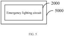
- the lighting device 5000 includes the emergency lighting circuit 2000 mentioned above.
- the lighting device 5000 may be an emergency lighting centralized power supply or a self-contained power type lamp.
- the emergency lighting centralized power supply is a non centralized control type emergency lighting centralized power supply.
- the automatic power supply type lamp is a self-contained power supply non centralized control type lamp.
Landscapes
- Circuit Arrangement For Electric Light Sources In General (AREA)
- Circuit Arrangements For Discharge Lamps (AREA)
Abstract
Description
- The present application claims the priority of the
Chinese patent application titled "Hysteresis Circuit, Emergency Lighting Circuit and Lighting Device" filed on August 16, 2021, with application number 202110936145.2 - The present application relates to a field of lighting circuit technology, specifically to a hysteresis circuit, an emergency lighting circuit, and a lighting device.
- Lighting that is activated due to the failure of the normal lighting power supply is called as emergency lighting. The emergency lighting is different from ordinary lighting, and the emergency lighting includes three types: backup lighting, evacuation lighting, and safety lighting. The emergency lighting is an important safety facility in modern public building and industrial building, and it is closely related to personal safety and building safety. When a building experiences a fire or other disaster, and the power supply is interrupted, the emergency lighting plays an important role in personnel evacuation, fire rescue work, and the continued operation or necessary operation and disposal of important production and work.
- At present, the fire emergency lighting and evacuation indication system includes the power supply of emergency lighting fixtures and evacuation indication fixtures. For non centrally controlled emergency lighting centralized power supply, there are the following regulations, there are the following regulations: when the main power supply voltage of the lamp works at any voltage within the range of 60% -80% of its rated voltage, the status indicator lights and the relays of the emergency lighting centralized power supply should not have multiple switching phenomena. If multiple switching phenomena occur, it will inevitably cause ripple and instability of the main power supply voltage of the lamp.
- Therefore, the relevant technical personnel proposed a scheme as shown in
FIG. 1 to determine the situation of the main power supply voltage of the lamp. As shown inFIG. 1 , for non isolated power supplies, the ADC sampling value is obtained by using a microcontroller U4, and the following logical judgment is made: determining whether the input voltage Vbus has reached the trigger action voltage point, and when it returns to normal operation, determining whether the input voltage Vbus has reached the reverse recovery voltage point. The trigger action voltage point refers to the voltage value corresponding to reaching a preset function (such as triggering an emergency function), and the reverse recovery voltage point refers to the voltage value corresponding to before restoring to the preset function (such as restoring to normal operation). - However, the above scheme has specific limitations, which include: 1) only for non isolated power sources,where the input voltage and the microcontroller are grounded, making the scheme suitable for applications with broad requirements for product safety design; 2) only suitable for circuits with microcontroller control and suitable ADC sampling value detection ports.
- Therefore, it is necessary to propose solutions for existing technical problems.
- The purpose of the present application is to provide a hysteresis circuit, an emergency lighting circuit, and a lighting device, which aims to detect a sampling voltage associated with the input voltage. When the sampling voltage is detected to decrease to the trigger action voltage point, the corresponding level of the output signal is controlled to flip until it is detected that the sampling voltage has risen to the reverse recovery voltage point, the corresponding level of the output signal is controlled to flip again, so as to achieve timely and accurate monitoring of the input voltage status, further improving the reliability and safety of the product.
- According to one aspect of the present application, an embodiment of the present application provides a hysteresis circuit, the hysteresis circuit includes: a voltage detection module, configured to receive an input voltage and generate a sampling voltage based on the input voltage, and detect the sampling voltage; a solation coupling module, configured to control an output signal of the isolation coupling module based on the sampling voltage; and a voltage adjusting module, configured to adjust the sampling voltage; in a case that the voltage detection module detects that the sampling voltage is less than a first set value, an optocoupler in the isolation coupling module is controlled to be in an isolating state, so that the output signal of the isolation coupling module is a first level signal, and the voltage adjusting module begins to adjust the sampling voltage; in a case that the voltage detection module detects that the sampling voltage is greater than a second set value, the optocoupler is controlled to be in a coupling state, so that the output signal of the isolation coupling module is a second level signal, and the voltage adjusting module stops adjusting the sampling voltage, the second set value is greater than the first set value, and a difference between the second set value and the first set value is greater than a preset threshold, the first level signal is different from the second level signal.
- Optionally, the voltage detection module comprises: a first voltage divider resistor, a second voltage divider resistor, a first capacitor, and a voltage regulator; a first end of the first voltage divider resistor receives the input voltage, and a second end of the first voltage divider resistor is connected to a first end of the second voltage divider resistor to form a first node, the first voltage divider resistor and the second voltage divider resistor are configured to divide the input voltage so that a voltage of the first node is the sampling voltage, the first end of the second voltage divider resistor is electrically connected to a first end of the first capacitor and a first pin of the voltage regulator, and a second end of the second voltage divider resistor is electrically connected to a second end of the first capacitor and a third pin of the voltage regulator, respectively; a first end of the first capacitor is electrically connected to the first pin of the voltage regulator, and the second end of the first capacitor is electrically connected to the third pin of the voltage regulator; a second pin of the voltage regulator is connected to the isolation coupling module, the third pin of the voltage regulator is connected to a power ground, and the first pin of the voltage regulator is configured to obtain the sampling voltage.
- Optionally, in a case that the sampling voltage obtained by the first pin of the voltage regulator is less than the first set value, the voltage regulator is in a cut-off state; in a case that the sampling voltage obtained by the first pin of the voltage regulator is greater than the second set value, the voltage regulator is in a conductive state.
- Optionally, the isolation coupling module further comprises: a fifth resistor and a sixth resistor; a first end of the fifth resistor receives a first side supply voltage, and a second end of the fifth resistor is electrically connected to a positive electrode of a light-emitting diode on a primary side of the optocoupler; a first end of the sixth resistor is connected to a second side supply voltage, and a second end of the sixth resistor is electrically connected to a collector electrode of a triode on a secondary side of the optocoupler; a negative electrode of the light-emitting diode on the primary side of the optocoupler is electrically connected to a second pin of the voltage regulator in the voltage detection module, and an emitter electrode of the triode on the secondary side of the optocoupler is connected to a signal ground.
- Optionally, the voltage adjusting module comprises: a first voltage stabilizing transistor, a seventh resistor, an eighth resistor, a ninth resistor, and a first switching transistor; a first end of the first voltage stabilizing transistor is electrically connected to a first end of the seventh resistor, and a second end of the first voltage stabilizing transistor is electrically connected to a second end of the fifth resistor in the isolation coupling module; a second end of the seventh resistor is electrically connected to a first end of the eighth resistor and a control end of the first switching transistor, respectively; a first end of the eighth resistor is electrically connected to a control end of the first switching transistor, and a second end of the eighth resistor is electrically connected to a first end of the first switching transistor; a first end of the ninth resistor is electrically connected to a first end of a second voltage divider resistor in the voltage detection module, and a second end of the ninth resistor is electrically connected to a second end of the first switching transistor; a first end of the first switching transistor is respectively connected to a second end of the second voltage divider resistor in the voltage detection module and a power ground.
- Optionally, a second voltage divider resistor in the voltage detection module and a ninth resistor in the voltage adjusting module are variable resistors.
- Optionally, the first set value is configured to be associated with a resistance value of the second divider resistor; and the second set value is configured to be associated with a resistance value of the ninth resistor.
- Optionally, a power ground connected to a voltage regulator in the voltage detection module on a primary side of the optocoupler is not in common ground with a signal ground connected to the secondary side of the optocoupler.
- According to another aspect of the present application, an embodiment of the present application provides an emergency lighting circuit, and the emergency lighting circuit comprises a rectification circuit, configured to convert an input AC power into a DC power to provide the DC power to the hysteresis circuit; the hysteresis circuit in any one of the embodiments of the present application; a control circuit, configured to control an operation of an indicator light or a relay based on the output signal of the isolation coupling module in the hysteresis circuit.
- According to another aspect of the present application, an embodiment of the present application provides a lighting device, and the lighting device comprises an emergency lighting circuit as described in any one of the embodiments of the present application.
- The hysteresis circuit, the emergency lighting circuit, and the lighting device provided by the embodiments of the present application aim to detect a sampling voltage associated with the input voltage. When the sampling voltage is detected to decrease to the trigger action voltage point, the corresponding level of the output signal is controlled to flip until it is detected that the sampling voltage has risen to the reverse recovery voltage point, the corresponding level of the control output signal is controlled to flip again, so as to achieve hysteresis design for the input voltage detection, thereby achieving timely and accurate monitoring of input voltage status, and ensuring that emergency lighting circuits work according to specified requirements, and improving product reliability and safety.
- Based on the drawings, detailed descriptions of the specific embodiments of the present application will make the technical solutions and other beneficial effects of the present application obvious.
-
FIG. 1 is a schematic diagram of a hysteresis circuit in the prior art. -
FIG. 2 is a schematic diagram of an architecture of a hysteresis circuit provided by an embodiment of the present application. -
FIG. 3 is a schematic diagram of a hysteresis circuit provided by an embodiment of the present application. -
FIG. 4 is a schematic diagram of an emergency lighting circuit provided by an embodiment of the present application. -
FIG. 5 is a schematic diagram of a lighting device provided by an embodiment of the present application. - The following will provide a clear and complete description of the technical solution in the embodiments of the present application, in conjunction with the accompanying drawings. Obviously, the described embodiments are only a portion of the embodiments of the present application, not the entire embodiments. Based on the embodiments in the present application, all other embodiments obtained by those skilled in the art without creative labor fall within the protection scope in the present application.
- The terms "first" and "second" in the text are only used to describe the purpose and cannot be understood as indicating or implying relative importance or implying the quantity of technical features indicated. Therefore, the features limited to "first" and "second" may explicitly or implicitly include one or more of the features. In the descriptions of the present application, "a plurality of" means two or more, unless otherwise specified.
- In the descriptions of the present application, it should be noted that unless otherwise specified and limited, the terms "installation", "connection", and "coupling" should be broadly understood, for example, they can be fixed connections, detachable connections, or integrated connections; they can be mechanical connections, electrical connections, or signal connections with each other; they can be direct connection or indirect connection through an intermediate medium, and can be the internal connection of two components or the interaction relationship between two components. For ordinary technical personnel in this field, the specific meanings of the above terms in the present application can be understood based on specific circumstances.
- The following disclosure provides many different implementation methods or examples to implement the different structures of the present application. In order to simplify the disclosure of the present application, specific examples of components and arrangements will be described below. Of course, they are only examples and are not intended to limit the present application. In addition, the present application may repeat reference numbers and/or reference letters in different examples for the purpose of simplification and clarity, and does not indicate the relationship between the various embodiments and/or arrangements discussed.
-
FIG. 2 is a schematic diagram of an architecture of a hysteresis circuit provided by an embodiment of the present application. - As shown in
FIG. 2 , at least one embodiment of the present application provides ahysteresis circuit 1000, thehysteresis circuit 1000 includes avoltage detection module 110 configured to receive an input voltage Vbus, generate a sampling voltage VA based on the input voltage Vbus, and detect the sampling voltage VA; anisolation coupling module 120 configured to control the output signal Vbus_c of theisolation coupling module 120 based on the sampling voltage; avoltage adjusting module 130 configured to adjust the sampling voltage VA; in a case that thevoltage detection module 110 detects that the sampling voltage VA is less than a first set value, the optocoupler U1 in theisolation coupling module 120 is controlled to be in an isolating state, so that the output signal Vbus_c of theisolation coupling module 120 is a first level signal, and thevoltage adjusting module 130 starts adjusting the sampling voltage VA; in a case that thevoltage detection module 110 detects that the sampling voltage VA is greater than a second set value, the optocoupler U1 is controlled to be in a coupling state, so that the output signal Vbus_c of theisolation coupling module 120 is a second level signal, and thevoltage adjusting module 130 stops adjusting the sampling voltage VA, the second set value is greater than the first set value, and the difference between the second set value and the first set value is greater than a preset threshold. The first level signal is different from the second level signal. - This design can achieve hysteresis design for input voltage detection, enabling timely and accurate judgment of the status of the input voltage, and also ensuring that the corresponding emergency lighting circuit operates normally according to specified requirements, thereby improving the reliability and safety of the lighting device.
- The following will further describe the structure of the
hysteresis circuit 1000 in conjunction withFIG. 3 . - As shown in
FIG. 2 andFIG. 3 , an embodiment of the present application provides ahysteresis circuit 1000, which includes avoltage detection module 110, anisolation coupling module 120, and avoltage adjusting module 130. - Specifically, the
voltage detection module 110 may include: a first voltage divider resistor and a second voltage divider resistor, a first capacitor C1, and a voltage regulator U2. A first end of the first voltage divider resistor receives the input voltage, and a second end of the first voltage divider resistor is connected to a first end of the second voltage divider resistor to form a first node A. The first voltage divider resistor and the second voltage divider resistor are configured to divide the input voltage so that the voltage of the first node A is the sampling voltage. In the present embodiment, the first voltage divider resistor may include a first resistor R1, a second resistor R2, and a third resistor R3, but in other partial embodiments, the first voltage divider resistor may include a plurality of resistors or only one resistor. The second voltage divider resistor is the fourth resistor R4 (which will be described below as the fourth resistor). As shown inFIG. 2 , specifically, a first end of the first resistor R1 receives the input voltage Vbus, and a second end of the first resistor R1 is electrically connected to a first end of the second resistor R2. A second end of the second resistor R2 is electrically connected to a first end of the third resistor R3, and a second end of the third resistor R3 is electrically connected to a first end of the fourth resistor R4, a first end of the first capacitor C1, and a first pin of the voltage regulator U2, respectively. The first end of the fourth resistor R4 is electrically connected to the first end of the first capacitor C1 and the first pin of the voltage regulator U2, respectively. A second end of the fourth resistor R4 is electrically connected to a second end of the first capacitor C1 and a third pin of the voltage regulator U2, respectively. The first end of the first capacitor C1 is electrically connected to the first pin of the voltage regulator U2, and the second end of the first capacitor C1 is electrically connected to the third pin of the voltage regulator U2. A second pin of the voltage regulator U2 is connected to theisolation coupling module 120, and the third pin of the voltage regulator U2 is connected to a power ground. - In the
voltage detection module 110, the first resistor R1, the second resistor R2, the third resistor R3, and the fourth resistor R4 are sequentially connected in series. The first resistor R1 receives the input voltage Vbus. The input voltage Vbus may be a DC voltage, which can be obtained through the rectification circuit in the emergency lighting circuit. In the present embodiment, the resistance values of the first resistor R1, the second resistor R2, and the third resistor R3 are the same and different from the resistance value of the fourth resistor R4. The fourth resistor R4 and the three resistors mentioned above (the first resistor R1, the second resistor R2, and the third resistor R3) divide the input voltage to obtain the sampling voltage VA of the first node A. As shown inFIG. 3 , the voltage of the first node A is the sampling voltage VA, which is the same in the following text. In this case, the voltage obtained from the first pin of the voltage regulator U2 is the sampling voltage VA. When the sampling voltage obtained by the first pin of the voltage regulator U2 is less than the first set value, the voltage regulator U2 is in a cut-off state; when the sampling voltage obtained by the first pin of the voltage regulator U2 is greater than the second set value, the voltage regulator U2 is in a conductive state. Therefore, the voltage regulator U2 can be regarded as a switching element. - Furthermore, the first capacitor C1 is connected in parallel with the fourth resistor R4, which is configured to filter the voltage signal received by the first pin of the voltage regulator U2. In the present embodiment, the voltage regulator U2 may adopt a TL43 1M type voltage regulator, with an internal reference voltage of 2.5V. If other models of voltage regulators are used, their internal reference voltage may be different.
- The
isolation coupling module 120 includes a fifth resistor R5, a sixth resistor R6, and an optocoupler U1. A first end of the fifth resistor R5 receives a first side supply voltage VF, and a second end of the fifth resistor R5 is electrically connected to a positive electrode of a light-emitting diode on a primary side of the optocoupler U1. A first end of the sixth resistor R6 is connected to a second side supply voltage VDD, and a second end of the sixth resistor R6 is electrically connected to a collector electrode of a triode on a secondary side of the optocoupler U1. A negative electrode of the light-emitting diode on the primary side of the optocoupler U1 is electrically connected to a second pin of the voltage regulator U2 in thevoltage detection module 110, and an emitter electrode of the triode on the secondary side of the optocoupler U1 is connected to a signal ground. - In the present embodiment, the optocoupler U1 adopts an EL817 type optocoupler, which is not limited to this. When the light-emitting diode on the primary side of the optocoupler U1 is conductive, the triode on the secondary side works normally, causing the optocoupler U1 to be in a coupling state. When the light-emitting diode on the primary side of the optocoupler U1 is cut off, the triode on the secondary side does not work, so that the optocoupler U1 is in an isolating state.
- It should be noted that, the first side supply voltage VF received by the first end of the fifth resistor R5 and the second side supply voltage VDD received by the first end of the sixth resistor R6 are both fixed supply voltages. In addition, in the present embodiment, the power ground connected to the voltage regulator U2 in the
voltage detection module 110 on the primary side of the optocoupler U1 is not in common ground with the signal ground connected to the secondary side of the optocoupler U1. Of course, in other embodiments, the power ground and the signal ground can be grounded together (applicable to non isolated power sources). - Continuing to refer to
FIG. 2 andFIG. 3 , thevoltage adjusting module 130 includes: a first voltage stabilizing transistor ZD1, a seventh resistor R7, an eighth resistor R8, a ninth resistor R9, and a first switching transistor Q1. A first end of the first voltage stabilizing transistor ZD1 is electrically connected to a first end of the seventh resistor R7, and a second end of the first voltage stabilizing transistor ZD1 is electrically connected to the second end of the fifth resistor R5 in theisolation coupling module 120. A second end of the seventh resistor R7 is electrically connected to a first end of the eighth resistor R8 and a control end of the first switching transistor Q1, respectively. A first end of the eighth resistor R8 is electrically connected to the control end of the first switching transistor Q1, and a second end of the eighth resistor R8 is electrically connected to a first end of the first switching transistor Q1. A first end of the ninth resistor R9 is electrically connected to a first end of the fourth resistor R4 in thevoltage detection module 110, and a second end of the ninth resistor R9 is electrically connected to a second end of the first switching transistor Q1. The first end of the first switching transistor Q1 is respectively connected to a second end of the fourth resistor R4 in thevoltage detection module 110 and a power ground. - In the present embodiment, the ninth resistor R9 is connected in series with the first switching transistor Q1, and then connected in parallel with the fourth resistor R4. When the first switching transistor Q1 is in a conductive state, its conducting resistance is connected in series with the ninth resistor R9, and then in parallel with the fourth resistor R4. When the first switching transistor Q1 is in the cut-off state, its resistance value is very high, after being connected in series with the ninth resistor R9, the effect on the resistance value of the fourth resistor R4 connected in parallel can be ignored. In other words, when the first switching transistor Q1 is in a conductive state, the ground resistance of the first pin of the voltage regulator U2 is an equivalent resistance corresponding to the parallel connection of the fourth resistor R4, the ninth resistor R9, and the conduction resistance of the first switching transistor Q1. When the first switching transistor Q1 is in the cut-off state, the resistance value of the first switching transistor Q1 is very large. Therefore, the ground resistance of the first pin of the voltage regulator U2 is the fourth resistor R4. In this way, when the first switching transistor Q1 is turned on, the ground resistance of the first pin of the voltage regulator U2 is smaller than the ground resistance of the first pin of the voltage regulator U2 when the first switching transistor Q1 is turned off.
- Optionally, in the present embodiment, the fourth resistor R4 in the
voltage detection module 110 and the ninth resistor R9 in thevoltage adjusting module 130 are variable resistors. When the input voltage remains constant and the resistance value of the fourth resistor R4 increases, the sampling voltage VA increases. When the input voltage remains unchanged and the resistance value of the fourth resistor R4 decreases, the sampling voltage VA decreases. Furthermore, in the case where the first switching transistor Q1 is in a conductive state, as the resistance value of the ninth resistor R9 increases, the hysteresis voltage decreases. When the resistance value of the ninth resistor R9 decreases, the hysteresis voltage increases. The hysteresis voltage will be further explained in the following text. Therefore, the first set value (i.e. trigger voltage action point) can be configured to be associated with the resistance value of the fourth resistor, and the second set value (i.e. reverse recovery voltage point) can be configured to be associated with the resistance value of the ninth resistor. - The following will further explain the working principle of the
hysteresis circuit 1000. - When the input voltage Vbus is different, the sampling voltage VA changes accordingly. If the input voltage is high, the sampling voltage VA is high. If the input voltage is low, the sampling voltage VA is low.
- If the input voltage Vbus decreases and gradually decreases to the following situation: when the sampling voltage VA is less than the internal reference voltage of the voltage regulator U2, the sampling voltage VA reaches the trigger voltage action point (i.e. the first set value), and the voltage regulator U2 enters the cut-off state, then the light-emitting diode on the primary side of the optocoupler U1 is not conducting (i.e. in the cut-off state), and the optocoupler U1 is in an isolating state. When the optocoupler U1 is in an isolating state, the output signal Vbus_c of the
isolated coupling module 120 is the first level signal. In the present embodiment, the first level signal is a high level. In this case, due to the cut-off state of the light-emitting diode on the primary side of the optocoupler U 1, that is, the first pin of the optocoupler U1 shown inFIG. 3 is at a high level, the first switching transistor Q1 is in a conductive state, therefore, its conducting resistance is connected in series with the ninth resistor R9, and then connected in parallel with the fourth resistor R4, resulting in a decrease of the sampling voltage VA. - If the input voltage Vbus changes from decreasing to increasing and gradually increases. When the input voltage Vbus returns to the original input voltage, the sampling voltage VA is still less than the internal reference voltage of the voltage regulator U2, because the conducting resistance of the first switching transistor Q1 is connected in series with the ninth resistor R9 and then in parallel with the fourth resistor R4.
- Next, the input voltage Vbus continues to increase until the following situation occurs: when the sampling voltage VA is greater than the internal reference voltage of the voltage regulator U2, the sampling voltage VA reaches the reverse recovery voltage point (i.e. the second set value), and the voltage regulator U2 enters the conductive state. Therefore, the light-emitting diode on the primary side of the optocoupler U1 is in the conductive state, and the optocoupler U1 is in the coupling state. When the optocoupler U1 is in the coupling state, the output signal Vbus_c of the
isolation coupling module 120 changes from the first level signal to the second level signal. In the present embodiment, the second level signal is a low-level signal, which is different from the first level signal. If the first level signal is a high-level signal and the second level signal is a low-level signal, then these two signals are opposite. Therefore, the output signal Vbus_c of theisolation coupling module 120 changes from high level to low level. In this case, due to the conductive state of the light-emitting diode on the primary side of the optocoupler U1, that is, the first pin of the optocoupler U1 shown inFIG. 3 is at a low level, the first switching transistor Q1 is in a cut-off state. Therefore, the resistance value of the first switching transistor Q1 is very high, after being connected in series with the ninth resistor R9, the effect on the resistance value of the fourth resistor R4 connected in parallel can be ignored, resulting in an increase of the sampling voltage VA. Therefore, it can further ensure that the sampling voltage VA is greater than the internal reference voltage of the voltage regulator U2, thereby enabling the output signal Vbus_c of theisolation coupling module 120 remains a low-level signal. - It should be noted that the second set value is greater than the first set value, and the difference between the second set value and the first set value is greater than the preset threshold, the preset threshold is related to the resistance values of the ninth resistor R9 and the first switching transistor Q1 in the
voltage adjusting module 130. Therefore, the voltage value corresponding to the reverse recovery voltage point is greater than the voltage value corresponding to the trigger action voltage point. Furthermore, the trigger action voltage point (i.e. the point corresponding to the action voltage) is related to the resistance value of the fourth resistor R4. The reverse recovery voltage point (i.e. the point corresponding to the hysteresis voltage) is related to the resistance values of the ninth resistor R9 and the first switching transistor Q1. When the first switching transistor Q1 is in a conductive state, the hysteresis voltage decreases as the resistance value of the ninth resistor R9 increases. When the resistance value of the ninth resistor R9 decreases, the hysteresis voltage increases. - In the
hysteresis circuit 1000 provided by any one of the embodiments of the present application, a hysteresis design for detecting the input voltage is achieved by setting a trigger action voltage point and a reverse recovery voltage point with a certain voltage difference, which enables timely and accurate judgment of the state of the input voltage, further ensuring that the corresponding emergency lighting circuit operates normally under specified requirements, and improving the reliability and safety of the product. - In addition, in the
hysteresis circuit 1000 provided by any one of the embodiments of the present application, because the power ground connected to the primary side of the optocoupler U1 through the voltage regulator U2 in thevoltage detection module 110 is not in common ground with the signal ground connected to the secondary side of the optocoupler U1, thehysteresis circuit 1000 can be suitable for isolating the power supply and does not use a microcontroller to detect sampling values, which makes that thehysteresis circuit 1000 described in the present application more widely applicable. - Based on the same invention concept, at least one embodiment of the present application further provides an emergency lighting circuit.
- As shown in
FIG. 4 , theemergency lighting circuit 2000 includes arectifier circuit 1100, ahysteresis circuit 1000, and acontrol circuit 1200. - Specifically, the
rectifier circuit 1100 is configured to convert the input AC power into DC power to provide the DC power to thehysteresis circuit 1000. - The hysteresis circuit is the
hysteresis circuit 1000 described in any one of the previous embodiments, and its specific structure and working principle are described above, which will not be repeated here. - The
control circuit 1200 is configured to control the output signal Vbus_c of theisolation coupling module 120 in thehysteresis circuit 1000 to control whether the indicator light (not shown in the figure) or relay (not shown in the figure) is working. - When determining the voltage value corresponding to the output signal Vbus_c is less than the preset threshold, the status indicator light or relay is controlled to work; when determining the voltage value corresponding to the output signal Vbus_c is greater than or equal to the preset threshold, the status indicator light or the relay is controlled to stop working. The status indicator light or the relay is connected to the
control circuit 1200. In the present embodiment, when it is determined that the output signal Vbus_c is a low-level signal, the status indicator light is in the turn-on state, or the relay is controlled to enter the working state. When determining the output signal Vbus_c is a high-level signal, the status indicator light is in the turned-off state or the relay is controlled to stop working. - As described in the background, when the main power voltage of the lamp operates at any voltage within the range of 60% -80% of its rated voltage, the status indicator lights and the relays of the emergency lighting centralized power should not undergo multiple switching phenomena. If multiple switching phenomena occur, it will inevitably cause ripple and instability of the main power voltage of the lighting fixture. Therefore, the present application provides an
emergency lighting circuit 2000, which adopts thehysteresis circuit 1000 described above, for detecting and controlling the main power voltage (i.e. input voltage) of the lamp. - During the process of the main power voltage reducing to 60% to 80% of the rated voltage (i.e. the input voltage Vbus of the lamp is reduced from 100% of the rated voltage to 60% -80% of the rated voltage), the sampling voltage VA in the
hysteresis circuit 1000 decreases correspondingly with the decrease of the input voltage. When the trigger action voltage point is reached, the voltage regulator U2 is in the cut-off state, and the corresponding optocoupler U1 is in the isolating state, so that the output signal Vbus_c of theisolation coupling module 120 is a high-level signal. Because the output signal Vbus_c of theisolation coupling module 120 is a high-level signal (i.e. the output signal of the hysteresis circuit is a high-level signal), therefore, the status indicator light connected to thecontrol circuit 1200 in theemergency lighting circuit 2000 is in the turn-off state, or the relay connected to thecontrol circuit 1200 stops working. Correspondingly, the lamp connected to the relay also does not work, for example, the lamp is in the turn-off state. - During the process of the main power voltage rising to above 80% of the rated voltage (i.e. the input voltage Vbus of the lamp rises from 60% -80% of the rated voltage to above 80% of the rated voltage), the sampling voltage in the
hysteresis circuit 1000 increases correspondingly with the increase of the input voltage, and when the reverse recovery voltage point is reached, the voltage regulator U2 is in a conductive state, and the corresponding optocoupler U1 is in a conductive state, so that the output signal Vbus_c of theisolation coupling module 120 is a low-level signal. Because the output signal Vbus_c of theisolation coupling module 120 is a low-level signal (i.e. the output signal of the hysteresis circuit is a low-level signal), the status indicator light connected to thecontrol circuit 1200 in theemergency lighting circuit 2000 is in the lighting state. In this case, the relay connected to thecontrol circuit 1200 starts working, and accordingly, the lamp connected to the relay enters the working state, for example, the lamp is in the lighting state. - Because the setting of the trigger action voltage point and the reverse recovery voltage point with a certain voltage difference in the
hysteresis circuit 1000, it is possible to make timely and accurate judgments on the state of the input voltage, furthermore, it can also ensure that the correspondingemergency lighting circuit 2000 operates normally under specified requirements (i.e., when the main power voltage drops to the range of 60% -80% of its rated voltage, the status indicator light or the relay does not work, and when the main power voltage rises to more than 80% of its rated voltage, the status indicator light or the relay enters the working state), which can improve the reliability and safety of the lamp. - Based on the same invention concept, at least one embodiment of the present application further provides a lighting device.
- As shown in
FIG. 5 , thelighting device 5000 includes theemergency lighting circuit 2000 mentioned above. Thelighting device 5000 may be an emergency lighting centralized power supply or a self-contained power type lamp. In some embodiments, the emergency lighting centralized power supply is a non centralized control type emergency lighting centralized power supply. In other embodiments, the automatic power supply type lamp is a self-contained power supply non centralized control type lamp. When the main power voltage of these devices drops to the range of 60% -80% of their rated voltage, the status indicator light or the relay does not work. When the main power voltage of these devices rises to more than 80% of the rated voltage, the status indicator light or the relay enters the working state, thereby improving the safety and reliability of the lighting device. - In the above embodiments, the descriptions of each embodiment have their own emphasis. For parts that are not detailed in one embodiment, please refer to the relevant descriptions of other embodiments.
- The above provides a detailed introduction to a hysteresis circuit, an emergency lighting circuit, and a lighting device provided by the embodiments of the present application. Specific examples are applied in this article to explain the principles and implementation methods of the present application. The above embodiments are only used to help understand the technical solution and its core idea of the present application; ordinary technical personnel in this field should understand that they can still modify the technical solutions recorded in the aforementioned embodiments, or equivalently replace some of the technical features; and these modifications or replacements do not make the essence of the corresponding technical solutions deviate from the scope of the technical solutions of the various embodiments of the present application.
Claims (10)
- A hysteresis circuit, comprising:a voltage detection module, configured to receive an input voltage and generate a sampling voltage based on the input voltage, and detect the sampling voltage;a solation coupling module, configured to control an output signal of the isolation coupling module based on the sampling voltage; anda voltage adjusting module, configured to adjust the sampling voltage;wherein in a case that the voltage detection module detects that the sampling voltage is less than a first set value, an optocoupler in the isolation coupling module is controlled to be in an isolating state, so that the output signal of the isolation coupling module is a first level signal, and the voltage adjusting module begins to adjust the sampling voltage; in a case that the voltage detection module detects that the sampling voltage is greater than a second set value, the optocoupler is controlled to be in a coupling state, so that the output signal of the isolation coupling module is a second level signal, and the voltage adjusting module stops adjusting the sampling voltage, the second set value is greater than the first set value, and a difference between the second set value and the first set value is greater than a preset threshold, the first level signal is different from the second level signal.
- The hysteresis circuit according to claim 1, wherein the voltage detection module comprises: a first voltage divider resistor, a second voltage divider resistor, a first capacitor, and a voltage regulator; a first end of the first voltage divider resistor receives the input voltage, and a second end of the first voltage divider resistor is connected to a first end of the second voltage divider resistor to form a first node, the first voltage divider resistor and the second voltage divider resistor are configured to divide the input voltage so that a voltage of the first node is the sampling voltage, the first end of the second voltage divider resistor is electrically connected to a first end of the first capacitor and a first pin of the voltage regulator, and a second end of the second voltage divider resistor is electrically connected to a second end of the first capacitor and a third pin of the voltage regulator, respectively; a first end of the first capacitor is electrically connected to the first pin of the voltage regulator, and the second end of the first capacitor is electrically connected to the third pin of the voltage regulator; a second pin of the voltage regulator is connected to the isolation coupling module, the third pin of the voltage regulator is connected to a power ground, and the first pin of the voltage regulator is configured to obtain the sampling voltage.
- The hysteresis circuit according to claim 2, wherein in a case that the sampling voltage obtained by the first pin of the voltage regulator is less than the first set value, the voltage regulator is in a cut-off state; in a case that the sampling voltage obtained by the first pin of the voltage regulator is greater than the second set value, the voltage regulator is in a conductive state.
- The hysteresis circuit according to claim 1, wherein the isolation coupling module further comprises: a fifth resistor and a sixth resistor; a first end of the fifth resistor receives a first side supply voltage, and a second end of the fifth resistor is electrically connected to a positive electrode of a light-emitting diode on a primary side of the optocoupler; a first end of the sixth resistor is connected to a second side supply voltage, and a second end of the sixth resistor is electrically connected to a collector electrode of a triode on a secondary side of the optocoupler; a negative electrode of the light-emitting diode on the primary side of the optocoupler is electrically connected to a second pin of the voltage regulator in the voltage detection module, and an emitter electrode of the triode on the secondary side of the optocoupler is connected to a signal ground.
- The hysteresis circuit according to claim 1, wherein the voltage adjusting module comprises: a first voltage stabilizing transistor, a seventh resistor, an eighth resistor, a ninth resistor, and a first switching transistor; a first end of the first voltage stabilizing transistor is electrically connected to a first end of the seventh resistor, and a second end of the first voltage stabilizing transistor is electrically connected to a second end of the fifth resistor in the isolation coupling module; a second end of the seventh resistor is electrically connected to a first end of the eighth resistor and a control end of the first switching transistor, respectively; a first end of the eighth resistor is electrically connected to a control end of the first switching transistor, and a second end of the eighth resistor is electrically connected to a first end of the first switching transistor; a first end of the ninth resistor is electrically connected to a first end of a second voltage divider resistor in the voltage detection module, and a second end of the ninth resistor is electrically connected to a second end of the first switching transistor; a first end of the first switching transistor is respectively connected to a second end of the second voltage divider resistor in the voltage detection module and a power ground.
- The hysteresis circuit according to claim 1, wherein a second voltage divider resistor in the voltage detection module and a ninth resistor in the voltage adjusting module are variable resistors.
- The hysteresis circuit according to claim 6, wherein the first set value is configured to be associated with a resistance value of the second divider resistor; and the second set value is configured to be associated with a resistance value of the ninth resistor.
- The hysteresis circuit according to claim 1, wherein a power ground connected to a voltage regulator in the voltage detection module on a primary side of the optocoupler is not in common ground with a signal ground connected to the secondary side of the optocoupler.
- An emergency lighting circuit, comprising:a rectification circuit, configured to convert an input AC power into a DC power to provide the DC power to the hysteresis circuit;the hysteresis circuit as claimed in any one of claims 1 to 8; anda control circuit, configured to control an operation of an indicator light or a relay based on the output signal of the isolation coupling module in the hysteresis circuit.
- A lighting device, comprising the emergency lighting circuit as claimed in claim 9.
Applications Claiming Priority (2)
| Application Number | Priority Date | Filing Date | Title |
|---|---|---|---|
| CN202110936145.2A CN113507772B (en) | 2021-08-16 | 2021-08-16 | Hysteresis circuit, emergency lighting circuit and lighting equipment |
| PCT/CN2022/111107 WO2023020331A1 (en) | 2021-08-16 | 2022-08-09 | Hysteresis circuit, emergency lighting circuit, and lighting device |
Publications (2)
| Publication Number | Publication Date |
|---|---|
| EP4387398A1 true EP4387398A1 (en) | 2024-06-19 |
| EP4387398A4 EP4387398A4 (en) | 2024-12-04 |
Family
ID=78015733
Family Applications (1)
| Application Number | Title | Priority Date | Filing Date |
|---|---|---|---|
| EP22857643.5A Pending EP4387398A4 (en) | 2021-08-16 | 2022-08-09 | HYSTERESIS CIRCUIT, EMERGENCY LIGHTING CIRCUIT AND LIGHTING DEVICE |
Country Status (3)
| Country | Link |
|---|---|
| EP (1) | EP4387398A4 (en) |
| CN (1) | CN113507772B (en) |
| WO (1) | WO2023020331A1 (en) |
Families Citing this family (3)
| Publication number | Priority date | Publication date | Assignee | Title |
|---|---|---|---|---|
| CN113507772B (en) * | 2021-08-16 | 2025-02-25 | 欧普照明股份有限公司 | Hysteresis circuit, emergency lighting circuit and lighting equipment |
| US12588125B2 (en) | 2021-08-16 | 2026-03-24 | Opple Lighting Co., Ltd. | Hysteresis circuit, emergency lighting circuit and lighting device |
| CN118658325B (en) * | 2024-08-20 | 2025-03-21 | 浙江中控信息产业股份有限公司 | An alternating current detection circuit, an alternating current detection system and a traffic control machine |
Family Cites Families (13)
| Publication number | Priority date | Publication date | Assignee | Title |
|---|---|---|---|---|
| CN101882879B (en) * | 2010-06-30 | 2013-10-02 | 海洋王照明科技股份有限公司 | Circuit converting constant current source to constant voltage source and light using same |
| US20150008894A1 (en) * | 2013-07-02 | 2015-01-08 | Lsi Corporation | Dynamic start-up circuit for hysteretic loop switched-capacitor voltage regulator |
| CN105098704A (en) * | 2015-07-06 | 2015-11-25 | 宁波微鹅电子科技有限公司 | Undervoltage protection circuit, undervoltage protection method and wireless power transmission device |
| CN106208656A (en) * | 2016-09-05 | 2016-12-07 | 株洲中车时代电气股份有限公司 | A kind of DC source under-voltage protective module |
| CN109525117B (en) * | 2017-09-20 | 2020-08-04 | 台达电子企业管理(上海)有限公司 | Control circuit and control method of flyback converter |
| CN207321095U (en) * | 2017-09-29 | 2018-05-04 | 深圳欧陆通电子股份有限公司 | A kind of protection not exported altogether and Hysteresis control circuit |
| CN111567146B (en) * | 2018-01-02 | 2022-09-23 | 昕诺飞控股有限公司 | Lighting driver, lighting system and control method |
| CN208955639U (en) * | 2018-09-04 | 2019-06-07 | 广东明丰电源电器实业有限公司 | An input overvoltage and undervoltage protection circuit |
| CN209215474U (en) * | 2018-11-12 | 2019-08-06 | 无锡市金赛德电子有限公司 | A voltage undervoltage alarm circuit with hysteresis |
| CN209559340U (en) * | 2019-03-06 | 2019-10-29 | 广州金升阳科技有限公司 | A kind of temperature protection and alarm circuit |
| CN111917103B (en) * | 2020-08-24 | 2025-02-28 | 柏宜照明(上海)股份有限公司 | A main power conversion detection circuit for a power supply IC that can be turned off for a power module |
| CN215991299U (en) * | 2021-08-16 | 2022-03-08 | 欧普照明股份有限公司 | Hysteresis circuit, emergency lighting circuit and lighting equipment |
| CN113507772B (en) * | 2021-08-16 | 2025-02-25 | 欧普照明股份有限公司 | Hysteresis circuit, emergency lighting circuit and lighting equipment |
-
2021
- 2021-08-16 CN CN202110936145.2A patent/CN113507772B/en active Active
-
2022
- 2022-08-09 WO PCT/CN2022/111107 patent/WO2023020331A1/en not_active Ceased
- 2022-08-09 EP EP22857643.5A patent/EP4387398A4/en active Pending
Also Published As
| Publication number | Publication date |
|---|---|
| CN113507772A (en) | 2021-10-15 |
| CN113507772B (en) | 2025-02-25 |
| WO2023020331A1 (en) | 2023-02-23 |
| EP4387398A4 (en) | 2024-12-04 |
Similar Documents
| Publication | Publication Date | Title |
|---|---|---|
| WO2023020331A1 (en) | Hysteresis circuit, emergency lighting circuit, and lighting device | |
| CN206235687U (en) | A kind of reliable detection circuit of AC dump signal | |
| CN101246198B (en) | Electric network power-fail detection circuit | |
| CN111917103A (en) | A main-standby power conversion detection circuit for a power supply module capable of turning off a power supply IC | |
| CN103683420B (en) | Voltage balancing circuit of series-connected super-capacitor module of electric automobile | |
| CN205248227U (en) | Multichannel fusing of metal alarm instruction circuit | |
| CN101711072B (en) | Constant current driving circuit, LED light source and locomotive light | |
| CN112147496B (en) | Electronic switch testing device and method | |
| EP4456673A1 (en) | Interface control circuit, control method and interface control device | |
| CN215991299U (en) | Hysteresis circuit, emergency lighting circuit and lighting equipment | |
| US12588125B2 (en) | Hysteresis circuit, emergency lighting circuit and lighting device | |
| CN112290519B (en) | High-reliability ground wire live detection protection circuit | |
| CN204906812U (en) | Compatible low pressure and permanent power output's of high pressure input LED circuit | |
| US11503689B1 (en) | Circuit protection apparatus, snubber circuit, and method of operating circuit protection apparatus | |
| CN210243751U (en) | AC three-phase power phase loss detection device | |
| CN106992501B (en) | Direct-current power supply capable of preventing power supply from being connected by mistake in output and LED lamp and control system thereof | |
| CN203352860U (en) | Intelligent identification power supply during power grid blackout or artificial-switching power-off | |
| CN206350187U (en) | LED drive circuit and LED | |
| CN111736088B (en) | Power state indicating circuit | |
| CN113359021B (en) | Static synchronous check relay and high-precision phase difference and amplitude difference judgment system | |
| CN111948508B (en) | Multifunctional instrument for online detection of electric thyristor element | |
| US9832827B2 (en) | Battery back up lamp using AC wiring activation | |
| CN203574359U (en) | Wide-voltage two-way indication bus isolator | |
| CN211959630U (en) | Day drive lamp circuit | |
| CN212259393U (en) | LED driver circuit |
Legal Events
| Date | Code | Title | Description |
|---|---|---|---|
| STAA | Information on the status of an ep patent application or granted ep patent |
Free format text: STATUS: THE INTERNATIONAL PUBLICATION HAS BEEN MADE |
|
| PUAI | Public reference made under article 153(3) epc to a published international application that has entered the european phase |
Free format text: ORIGINAL CODE: 0009012 |
|
| STAA | Information on the status of an ep patent application or granted ep patent |
Free format text: STATUS: REQUEST FOR EXAMINATION WAS MADE |
|
| 17P | Request for examination filed |
Effective date: 20240314 |
|
| AK | Designated contracting states |
Kind code of ref document: A1 Designated state(s): AL AT BE BG CH CY CZ DE DK EE ES FI FR GB GR HR HU IE IS IT LI LT LU LV MC MK MT NL NO PL PT RO RS SE SI SK SM TR |
|
| DAV | Request for validation of the european patent (deleted) | ||
| DAX | Request for extension of the european patent (deleted) | ||
| A4 | Supplementary search report drawn up and despatched |
Effective date: 20241031 |
|
| RIC1 | Information provided on ipc code assigned before grant |
Ipc: H05B 47/14 20200101AFI20241025BHEP |