EP4387110A1 - Fragment de circuit électrique avec topologie de commutation d'émission/réception - Google Patents
Fragment de circuit électrique avec topologie de commutation d'émission/réception Download PDFInfo
- Publication number
- EP4387110A1 EP4387110A1 EP22213012.2A EP22213012A EP4387110A1 EP 4387110 A1 EP4387110 A1 EP 4387110A1 EP 22213012 A EP22213012 A EP 22213012A EP 4387110 A1 EP4387110 A1 EP 4387110A1
- Authority
- EP
- European Patent Office
- Prior art keywords
- switch
- state
- electric circuit
- circuit fragment
- fragment
- Prior art date
- Legal status (The legal status is an assumption and is not a legal conclusion. Google has not performed a legal analysis and makes no representation as to the accuracy of the status listed.)
- Pending
Links
- 239000012634 fragment Substances 0.000 title claims abstract description 133
- 230000005291 magnetic effect Effects 0.000 claims abstract description 39
- 238000000034 method Methods 0.000 claims description 21
- 230000005294 ferromagnetic effect Effects 0.000 claims description 16
- 238000004590 computer program Methods 0.000 claims description 15
- 230000001131 transforming effect Effects 0.000 claims description 3
- 230000015654 memory Effects 0.000 description 7
- 230000005284 excitation Effects 0.000 description 5
- 230000009286 beneficial effect Effects 0.000 description 4
- 238000001514 detection method Methods 0.000 description 4
- 238000009413 insulation Methods 0.000 description 4
- 230000001419 dependent effect Effects 0.000 description 3
- 230000005669 field effect Effects 0.000 description 3
- 230000010355 oscillation Effects 0.000 description 3
- 230000000694 effects Effects 0.000 description 2
- 230000006870 function Effects 0.000 description 2
- 238000002955 isolation Methods 0.000 description 2
- 230000010358 mechanical oscillation Effects 0.000 description 2
- 230000003287 optical effect Effects 0.000 description 2
- 238000009738 saturating Methods 0.000 description 2
- 239000004065 semiconductor Substances 0.000 description 2
- 239000003990 capacitor Substances 0.000 description 1
- 238000004891 communication Methods 0.000 description 1
- 238000005516 engineering process Methods 0.000 description 1
- 230000036039 immunity Effects 0.000 description 1
- 238000005259 measurement Methods 0.000 description 1
- 230000003071 parasitic effect Effects 0.000 description 1
- 239000007787 solid Substances 0.000 description 1
- 230000007704 transition Effects 0.000 description 1
- 238000004804 winding Methods 0.000 description 1
Images


Classifications
-
- H—ELECTRICITY
- H03—ELECTRONIC CIRCUITRY
- H03F—AMPLIFIERS
- H03F3/00—Amplifiers with only discharge tubes or only semiconductor devices as amplifying elements
- H03F3/20—Power amplifiers, e.g. Class B amplifiers, Class C amplifiers
- H03F3/24—Power amplifiers, e.g. Class B amplifiers, Class C amplifiers of transmitter output stages
- H03F3/245—Power amplifiers, e.g. Class B amplifiers, Class C amplifiers of transmitter output stages with semiconductor devices only
-
- H—ELECTRICITY
- H03—ELECTRONIC CIRCUITRY
- H03F—AMPLIFIERS
- H03F3/00—Amplifiers with only discharge tubes or only semiconductor devices as amplifying elements
- H03F3/189—High-frequency amplifiers, e.g. radio frequency amplifiers
- H03F3/19—High-frequency amplifiers, e.g. radio frequency amplifiers with semiconductor devices only
- H03F3/195—High-frequency amplifiers, e.g. radio frequency amplifiers with semiconductor devices only in integrated circuits
-
- H—ELECTRICITY
- H03—ELECTRONIC CIRCUITRY
- H03F—AMPLIFIERS
- H03F3/00—Amplifiers with only discharge tubes or only semiconductor devices as amplifying elements
- H03F3/45—Differential amplifiers
- H03F3/45071—Differential amplifiers with semiconductor devices only
- H03F3/45076—Differential amplifiers with semiconductor devices only characterised by the way of implementation of the active amplifying circuit in the differential amplifier
- H03F3/45475—Differential amplifiers with semiconductor devices only characterised by the way of implementation of the active amplifying circuit in the differential amplifier using IC blocks as the active amplifying circuit
-
- H—ELECTRICITY
- H04—ELECTRIC COMMUNICATION TECHNIQUE
- H04B—TRANSMISSION
- H04B1/00—Details of transmission systems, not covered by a single one of groups H04B3/00 - H04B13/00; Details of transmission systems not characterised by the medium used for transmission
- H04B1/38—Transceivers, i.e. devices in which transmitter and receiver form a structural unit and in which at least one part is used for functions of transmitting and receiving
- H04B1/40—Circuits
- H04B1/44—Transmit/receive switching
-
- H—ELECTRICITY
- H03—ELECTRONIC CIRCUITRY
- H03F—AMPLIFIERS
- H03F2200/00—Indexing scheme relating to amplifiers
- H03F2200/294—Indexing scheme relating to amplifiers the amplifier being a low noise amplifier [LNA]
-
- H—ELECTRICITY
- H03—ELECTRONIC CIRCUITRY
- H03F—AMPLIFIERS
- H03F2200/00—Indexing scheme relating to amplifiers
- H03F2200/451—Indexing scheme relating to amplifiers the amplifier being a radio frequency amplifier
-
- H—ELECTRICITY
- H03—ELECTRONIC CIRCUITRY
- H03F—AMPLIFIERS
- H03F2203/00—Indexing scheme relating to amplifiers with only discharge tubes or only semiconductor devices as amplifying elements covered by H03F3/00
- H03F2203/45—Indexing scheme relating to differential amplifiers
- H03F2203/45616—Indexing scheme relating to differential amplifiers the IC comprising more than one switch, which are not cross coupled
-
- H—ELECTRICITY
- H03—ELECTRONIC CIRCUITRY
- H03F—AMPLIFIERS
- H03F2203/00—Indexing scheme relating to amplifiers with only discharge tubes or only semiconductor devices as amplifying elements covered by H03F3/00
- H03F2203/45—Indexing scheme relating to differential amplifiers
- H03F2203/45621—Indexing scheme relating to differential amplifiers the IC comprising a transformer for phase splitting the input signal
-
- H—ELECTRICITY
- H03—ELECTRONIC CIRCUITRY
- H03F—AMPLIFIERS
- H03F2203/00—Indexing scheme relating to amplifiers with only discharge tubes or only semiconductor devices as amplifying elements covered by H03F3/00
- H03F2203/45—Indexing scheme relating to differential amplifiers
- H03F2203/45726—Indexing scheme relating to differential amplifiers the LC comprising more than one switch, which are not cross coupled
Definitions
- the present invention relates to an electric circuit fragment with transmit/receive switch topology for or of an electric circuit, a method of bringing an electric circuit fragment in its transmit state or in its receive state and to a computer program for controlling an electric circuit fragment with transmit/receive switch topology.
- the present invention may be used in conjunction with a micro-magnetic resonator (MMR) that sometime also is referred to as a magneto-mechanical oscillator (MMO).
- MMR micro-magnetic resonator
- MMO magneto-mechanical oscillator
- the MMR may be employed, e.g., for wireless remote tracking and sensing, e.g., in entertainment, sports, or medical applications.
- the MMR may be used for body tracking and sensing.
- wireless remote tracking and sensing systems include inter alia optical systems having one or more cameras that capture the position of passive or active markers, as well as electromagnetic tracking systems based on LC-resonators.
- inertial motion capture technology based on inertial measurements units (IMU) containing a combination of gyroscope, magnetometer, and accelerometer, to measure rotational rates can be employed.
- mechanical, magnetic or magneto-mechanical systems are known for wireless remote tracking and sensing.
- Magneto-mechanical systems often include an MMR for implementing the wireless remote tracking and sensing functionality.
- the wireless remote tracking and sensing functionality generally includes a magnetic excitation of a mechanical resonance of a ferromagnetic object.
- an MMR detector system may include electronics comprising one or more coils and amplifiers.
- a transmitter coil may be used for generating an oscillating magnetic field for excitation of a mechanical resonance of a ferromagnetic object.
- the mechanical resonance of the ferromagnetic object generates an oscillating magnetic field that can be detected as an external oscillating magnetic field by a sensor coil.
- MMRs enabling a more sensitive and reliable tracking and sensing functionality.
- the present invention is based on the objective of providing an electric circuit fragment for or of an electric circuit that provides an improved transmit/receive switch topology.
- the present invention is based on the further objective of providing an improved method of bringing an electric circuit fragment in its transmit state or in its receive state.
- the present invention is based on the objective of providing a computer program for controlling an electric circuit fragment with an improved transmit/receive switch topology.
- an electric circuit fragment for or of an electric circuit has a transmit state and a receive state.
- the electric circuit fragment comprises at least one coil, a low noise amplifier, a first switch, a power amplifier, and a second switch.
- the at least one coil is configured for generating an oscillating magnetic field in the transmit state and/or for detecting an external oscillating magnetic field in the receive state.
- the low noise amplifier is connected in series to the at least one coil and is configured for amplifying a first voltage signal induced in the at least one coil by the detected external oscillating magnetic field in the receive state.
- the first switch is connected in parallel to the low noise amplifier and is configured to shorten the low noise amplifier in the transmit state by switching the first switch into its conductive state or to switch into its isolating state in the receive state.
- the power amplifier is connected with its power amplifier output in series to the low noise amplifier and is configured for amplifying a received second voltage signal and for providing an amplified second voltage signal to the at least one coil in the transmit state, preferably, for generating the oscillating magnetic field in the transmit state.
- the second switch is arranged to connect the power amplifier output to a ground potential, and is configured to ground the power amplifier output in the receive state by switching to its conductive state and to switch in the transmit state to its isolating state.
- the invention includes the recognition that it is beneficial to use a single coil for both, generating an oscillating magnetic field and detecting an external oscillating magnetic field, e.g., to save space.
- the power amplifier (PA) generally applies a comparatively high voltage, e.g. 48V, to the coil.
- a comparatively weak signal e.g. few mV, is typically detected by the coil and is amplified by the low noise amplifier (LNA).
- LNA low noise amplifier
- the LNA typically needs to be shielded from the high voltages during the Tx phase.
- the electric circuit fragment due to its specific topology that has the PA and LNA not in parallel but in series.
- it is typically best to have a series connection of the PA and LNA and to alternately short one of the PA and LNA.
- the first switch can short the LNA and the second switch can ground the PA output.
- the first switch can be isolating, and the second switch can be conductive.
- the parasitic capacitance of the first switch when isolating does not deteriorate the Rx signal quality and the second switch can efficiently shorten any potential interference from the PA towards ground.
- This allows to neither destroy, overdrive nor saturate the sensitive LNA by shielding the LNA from the high voltages during Tx phase. This can be achieved by the specific topology of the electric circuit fragment.
- the first switch in the Rx state, can be isolating, and the second switch can be conductive.
- the first voltage signal then passes the LNA and the second switch without entering the PA at its power amplifier output.
- the first voltage signal travels from the coil towards the LNA.
- the power amplifier output In the Rx state, the power amplifier output can be grounded by switching the second switch in its conductive state. If the power amplifier output is grounded, interference with noise produced by the PA can be prevented.
- the function of the second switch is thus to shorten any potential interference from the PA towards ground during Rx phase, whilst during Tx phase, it does not have any negative side effect. Accordingly, during Rx phase, it is beneficial that the PA does not produce noise in the coil and during the Tx phase, the LNA advantageously can be protected from the high voltage of the PA.
- the first switch in the Tx state, can be conductive and the second switch can be isolating.
- the received second voltage signal can be amplified by the PA and pass the first switch without traversing the LNA, i.e., the input terminals of the LNA are shortened.
- the amplified second voltage signal travels from the PA towards the coil.
- the LNA can be shielded from the high voltages during Tx phase such that a risk of destroying, overdriving or saturating the LNA can be significantly reduced.
- the power amplifier is configured for amplifying the received second voltage signal and for providing an amplified second voltage signal of 10 V or more, preferably, of 40 V or more, e.g. in the order of 48 V.
- the first voltage signal received by the LNA may be 1 V or less, .e.g., in the order of a few mV.
- the external oscillating magnetic field can be generated by a ferromagnetic object of a micro-magnetic resonator and can be detected by the electric circuit fragment in its receive state.
- the term "external" thus refers to external from the electric circuit fragment.
- the electric circuit fragment is part of an electric circuit that may be composed of a plurality of individual electronic components, such as resistors, transistors, capacitors, inductors and diodes, connected, e.g., by conductive wires or traces through which electric current can flow.
- An amplifying transistor in the LNA can be a junction-gate field-effect transistor (jFET).
- the PA can have an H-bridge output stage.
- the H-bridge preferably, is an internal part of the PA and can be put in short mode.
- the PA includes a preferentially digitally switchable H-bridge
- no additional switch may be needed for the PA as the H-bridge can be put in a low impedance state by switching, e.g., one or both H-bridge's low side transistor to conductive state.
- the electric circuit fragment is configured such that the power amplifier output is configured as an H-bridge that is configured such as to short-circuit output terminals of the power amplifier output when in receive state.
- the first switch and/or the second switch is of a transistor-based switch type.
- the first switch and/or the second switch may be a field-effect transistor, e.g., a metal-oxide-semiconductor field-effect transistor (MOSFET).
- MOSFET metal-oxide-semiconductor field-effect transistor
- at least one of the first switch and/or the second switch may be a positive intrinsic negative (PIN) diode.
- PIN positive intrinsic negative
- a MOSFET is preferred over a PIN diode due to its generally lower costs.
- MOSFET it is further preferred that in a switching operation the low impedance of MOSFET is used for the conduction. This can be better than the high impedance state as the MOSFET may have considerable residual capacitance when in insulating state. This may avoid the use of generally costly PIN diodes as switches.
- still PIN diodes may be used as switches in addition or as an alternative to a MOSFET.
- the electric circuit fragment includes a single coil for generating an oscillating magnetic field in the transmit state and for detecting an external oscillating magnetic field in the receive state.
- the electric circuit fragment comprises a first coil for generating the oscillating magnetic field in the transmit state and a separate second coil for detecting the external oscillating magnetic field in the receive state. These two coils may strongly be inductively coupled, weakly coupled or not coupled at all.
- the electric circuit fragment may comprise a transformer connected in parallel to the low noise amplifier and in parallel to the first switch for transforming the first voltage signal provided by the at least one coil before it enters the low noise amplifier.
- a transformer e.g., a cored transformer, can be employed for amplifying the first voltage signal before it enters the LNA.
- using a transformer can be beneficial for impedance matching.
- the transformer can be used to transform the impedance of the coil to be more suitable for the LNA.
- the at least one coil i.e., the send and/or receive coil
- the LNA usually, at least when operating at very low noise, operates best at a much higher coil impedance.
- the transformer may solve this problem.
- the transformer makes it possible to operate a single ended LNA in the circuit, which means that one of the input terminals of the LNA is grounded. Technically, this may be similar to improving the common mode rejection ratio.
- the transformer may also be used to feed in some additional signals, like a Pilot tone, i.e. an additional very low power signal.
- the electric circuit fragment with a transformer comprises a third switch that is connected in series between the low noise amplifier and the transformer.
- the third switch preferably, is isolating in the Tx state and conductive in the Rx state.
- the additional third switch may improve the immunity of the LNA during the Tx phase.
- the amplified second voltage signal may interfere less with the LNA and therefore the acquisition may speed up.
- the LNA is not only protected from damage, for which the first switch is usually sufficient, but the residual send signal on the input of the LNA shall be so low that the LNA does not go into an undesired overdrive mode. Recuperating from overdrive mode generally may take time, and therefore the time between send and receive may be longer than necessary.
- MOSFET switches consist of two series MOSFET transistors with opposite direction. To reduce the capacitance, a voltage to the common pin of the two transistors relative to the terminal pins can be applied. This additional voltage may reduce the capacitance.
- the electric circuit fragment may comprise a fourth switch that is connected in parallel to the LNA and in parallel to the transformer.
- the fourth switch preferably, is isolating in the Rx state and conductive in the Tx state. That is, if the third switch and the fourth switch are present, preferably, in operation, the third switch is conductive and the fourth switch is isolating in the Rx state and the third switch is isolating and the fourth switch is conductive in the Tx state.
- these switches may work as voltage dividers.
- the third switch may be high-impedance
- fourth switch may be low impedance.
- undesired residual Tx signal arriving at the secondary winding of the transformer would see this voltage divider, and only a smallest fraction of that voltage would then appear across the shorted fourth switch, which is the same voltage as across the input of the LNA.
- the voltage division may work less efficient, as then the high impedance of the third switch would be in series with the also high impedance of the LNA input.
- the voltage division in that case may only be weakly reducing the voltage on the LNA input. Still, in certain applications, employing only the third switch and not the fourth switch may be sufficient.
- the voltage division may also work less efficient, as in that case, the fourth switch is basically parallel to the first switch, e.g., on the primary side of the transformer, where it may only marginally help. So whilst just using one switch, either the third switch or the fourth switch, is feasible, it is preferred to use the third and the fourth switches in pairs in in the electric circuit fragment.
- Adding more switches could be of advantage to improve the voltage division effect. Then the voltage division ladder may be continued in the same way, i.e., a fifth switch would be again in series, and sixth switch would be in parallel and so on.
- the transformer is a symmetrical transformer.
- a symmetrical transformer For example, it is possible that in the electric circuit fragment, an electrically single-ended configuration is translated into a balanced configuration, with a symmetrical power amplifier, symmetrical switches, a symmetrical coil, and a transformer having two symmetrical primary sides.
- a symmetrical PA in general, has both positive and negative power supply rails and a signal rises and falls centered on the 0 volts point exactly in between.
- the symmetrical transformer With the symmetrical transformer, it is possible to suppress common mode disturbances entering the LNA via the at least one coil.
- the present invention also relates to a detector system for a micro-magnetic resonator that can be used for tracking and/or sensing, preferably, for wireless remote tracking and/or sensing.
- the detector system comprises one or more ferromagnetic objects that can mechanically oscillate (upon excitation of the ferromagnetic object's mechanical resonance).
- the detector system has the capability to excite this mechanical oscillation of the ferromagnetic object by applying an oscillating magnetic field.
- this detector system has the capability of detecting and examining a received external oscillating magnetic field, which comes from the mechanical oscillation of the ferromagnetic object.
- the detector system comprises an electric circuit that includes the above-described electric circuit fragment, to enable these two capabilities
- the electric circuit fragment is arranged and configured for generating an oscillating magnetic field in the transmit state for excitation of a mechanical resonance of the ferromagnetic object such that the ferromagnetic object in turn generates an external oscillating magnetic field that can be detected by the electric circuit fragment in its receive state.
- the ferromagnetic object is or includes a permanent magnet.
- a mechanical resonance may be excited by means of an oscillating magnetic field transmitted by the electric circuit fragment's coil in the Tx state.
- the oscillating permanent magnet in the detector system may generate an external oscillating magnetic field that is picked up by a coil and amplified by the LNA.
- an oscillation i.e., a mechanical resonance
- the oscillation induces a voltage, i.e., the first voltage signal, in a coil that senses the oscillation in the Rx state.
- the detector system has the advantage that due to the specific topology of the electric circuit fragment, in the Rx state, the PA does not produce noise in the LNA and during the Tx state, the LNA is protected from the high power of the PA. Thereby, the detector system can work comparatively accurate and reliable.
- oscillating magnetic fields can be generated by the (plurality of) coil(s), that are powered/driven by the (at least) one PA of the electric circuit fragment.
- Tracking of the micro-magnetic resonator may be achieved based on a comparison of amplitudes of detected external oscillating magnetic fields. Therefore, if spatial information are required, a plurality coils, e.g., at least there coils, should be employed.
- Sensing may be achieved with the micro-magnetic resonator based on a detection of the self-decay frequency of the detected external oscillating magnetic field.
- the self-decay frequency is a property of the micro-magnetic resonator, and can differ from the excitation frequency in the Tx phase. For sensing, one coil, one LNA and one PA is sufficient.
- the present invention further relates to a method of operating the electric circuit fragment described above.
- Operating the electric circuit fragment may comprise bringing the electric circuit fragment in its transmit state or in its receive state.
- the method comprises the steps of:
- the method may further comprise switching the first switch from its conductive state in its isolating state or vice versa after a first predefined time period that begins with a switching of the second switch from its conductive state in its isolating state or vice versa. Additionally or alternatively, the method may further comprise switching the second switch from its conductive state in its isolating state or vice versa after a second predefined time period that begins with a switching of the first switch from its conductive state in its isolating state or vice versa.
- this delay may be different for turning on and turning off.
- the method it is possible to shorten the first and/or second switch e.g. at the PA but some additional time is added until the LNA switch, e.g., the first switch, is opened, especially, if there is residual current flowing through the coil.
- the method may further comprise switching the first switch into its conductive state while the second switch is still in its conductive state or comprising switching the second switch into its conductive state while the first switch is still in its conductive state. This is, because it may also be beneficial to have a short time both switches, i.e. the first and second switches, open to quickly bring any residual current in the coil to zero.
- the first switch may be opened relatively slowly, e.g., slower than the second switch.
- LNA overloading can be avoided.
- the present invention also relates to a computer program for controlling the electric circuit fragment described above.
- the computer program comprises program code such as, e.g., executable instructions, for causing the electric circuit fragment to switch from its transmit state into its receive state or vice versa by implementing the above-described method, when run on a computing device such as a personal computer (PC), a field programmable gate array (FPGA), microcontroller or a complex programmable logic device (CPLD), a processor, a processing circuit, or other computing device.
- the present invention also relates to a non-transitory computer readable data medium storing the computer program.
- the present invention relates to an electric circuit fragment for or of an electric circuit, the electric circuit fragment having a transmit state and a receive state.
- the electric circuit fragment comprises at least one coil, a low noise amplifier, a first switch, a power amplifier and a second switch.
- the at least one coil is configured for generating an oscillating magnetic field in the transmit state and/or for detecting an external oscillating magnetic field in the receive state.
- the low noise amplifier is connected in series to the at least one coil and is configured for amplifying a first voltage signal induced in the at least one coil.
- the first switch is connected in parallel to the low noise amplifier and is configured to shorten the inputs of the low noise amplifier in the transmit state.
- the power amplifier is connected with its power amplifier output in series to the low noise amplifier and is configured for amplifying a received second voltage signal and for providing an amplified second voltage signal to the at least one coil in the transmit state for generating the oscillating magnetic field.
- the second switch is arranged to connect the power amplifier output to a ground potential, and is configured to ground the power amplifier output in the receive state by switching to its conductive state.
- the present invention includes the following technical advantages: With the specific topology of the electric circuit fragment, shielding of the low noise amplifier can be achieved. This is achieved by an efficient decoupling between Tx state and Rx state of the electric circuit fragment. In particular, the electric circuit fragment provides an improved isolation of LNA with respect to noise in the Rx state. This leads to improved noise interference properties and improved Rx signal quality properties of the electric circuit fragment.
- this advantage is achieved by the specific topology of the electric circuit fragment enabling that during the Rx phase, the capacitance of the first switch does not deteriorate the Rx signal quality and the second switch very efficiently shortens any potential interference from the PA towards the ground.
- the electric circuit fragment as part of a detector system can therefore be used to implement a sensitive and reliable tracking and sensing functionality, e.g., as part of micro-magnetic resonators employed, e.g., in-body tracking and sensing.
- Fig. 1 schematically and exemplary shows an electric circuit fragment 100 with a topology known from the prior art, e.g., from WO 2015/043612 A1 .
- the electric circuit fragment 100 includes a power amplifier 102 that is connected in parallel to a low noise amplifier 104.
- the power amplifier 102 is connected in series to a first switch 106 and the low noise amplifier 104 is connected in series to a second switch 108.
- the first switch 106 can be conductive and the second switch 108 can be isolating or vice versa.
- the first switch 106 is conductive and the second switch 108 is isolating, such that an amplified voltage signal can be provided from the power amplifier 102 to a coil 110 for generating an oscillating magnetic field.
- the second switch 108 is conductive and the first switch 106 is isolating such that a voltage signal induced in the coil 110 by an external oscillating magnetic field can be provided to and amplified by the low noise amplifier 100.
- the switches 106, 108 there are several requirements on the switches 106, 108 such as low loss when conductive, low capacitance when isolating and fast transition time between the two modes, i.e., the transmit state and the receive state.
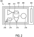
- Fig. 2 schematically and exemplary shows a detector system 200 for a micro-magnetic resonator, the detector system 200 comprising a ferromagnetic object 202 that is a permanent magnet and an electric circuit 204 comprising an electric circuit fragment 206.
- the electric circuit fragment 206 does not suffer from the intrinsic dilemma of the topology of the electric circuit fragment 100 described with respect to Fig. 1 .
- the power amplifier 208 and the low noise amplifier 210 are not connected in parallel as in the electric circuit fragment 100 but in series.
- the first switch 212 can be isolating and the second switch 214 can be conductive such that the capacitance of the first switch 212 does not the deteriorated the signal quality of a first voltage signal induced in the coil 216 and that is amplified by the low noise amplifier 210. Moreover, the second switch 214 efficiently shortens any potential interference from the power amplifier 208 towards the ground 218.
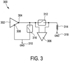
- Fig. 3 schematically and exemplary shows an electric circuit fragment 300 that may be used in the detector system 200 for a micro-magnetic resonator described with reference to Fig. 2 .
- the electric circuit fragment 300 essentially corresponds to the electric circuit fragment 200, but is shown and described with further details.
- the electric circuit fragment 300 includes a power amplifier 302 that is connected with its power amplifier output 304 in series to a low noise amplifier 306.
- the power amplifier 302 has a reference terminal 308 that is connected to ground 310.
- the electric circuit fragment 300 includes a first switch 312 that is connected in parallel to the low noise amplifier 306 and that can be used to short-circuit the inputs of the low noise amplifier 306 in the transmit state of the electric circuit fragment 300 by switching into its conductive state.
- the first switch 312 is switched into its isolating state.
- a first voltage signal induced in the coil 314 can be transmitted to and amplified by the low noise amplifier 306.
- the electric circuit fragment 300 includes a second switch 316 that connects the power amplifier output 304 to the ground 310 such that by switching the second switch 316 to its conductive state, the power amplifier output 304 can be grounded in the receive state of the electric circuit fragment 300.
- the second switch 316 can be switched to its isolating state such that an amplified second voltage signal can be transmitted from the power amplifier 302 via the conductive first switch 312 to the coil 314.
- the second terminal of the coil 314 is connected to ground 318. Grounds 310 and 318 are electrically connected.
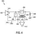
- Fig. 4 schematically and exemplary shows an electric circuit fragment 400 that may be used instead of electric circuit fragment 206 and the detector system 200 for a micro-magnetic resonator described with reference to Fig. 2 .
- the electric circuit fragment 400 includes a power amplifier 402, a first switch 404 and a second switch 406 as well as a coil 408 that are arranged and configured as described with reference to Fig. 3 .
- the power amplifier reference terminal 414 is connected to the ground 416.
- the power amplifier output 418 can be grounded by switching the second switch 406 into its conductive state. With its one end, the coil 408 is connected in series with the first switch 404 and with its other end, the coil 408 is connected to the ground 420.
- the electric circuit fragment 400 includes a transformer 410.
- the transformer 410 is connected in parallel to a low noise amplifier 412 and in parallel to the first switch 404 for transforming a first voltage signal provided by the coil 408 before it enters the low noise amplifier 412.
- the transformer 410 has a primary side 422 and a secondary side 424. With its primary side 422, the transformer 410 is connected in parallel to the first switch 404. With its secondary side 424, the transformer 410 is connected in parallel to the low noise amplifier 412. Moreover, with its secondary side 424, the transformer 410 is connected to the ground 426.
- Fig. 5 schematically and exemplary shows an electric circuit fragment 500 that may be used instead of electric circuit fragment 206 in the detector system for micro-magnetic resonators 200 described with reference to Fig. 2 .
- the electric circuit fragment comprises a power amplifier 502 that has a reference terminal 504 connected to the ground 506 and a power amplifier output 508 connected to a first switch 510 that can be switched into its conductive state in the transmit state of the electric circuit fragment 500 for transmitting an amplified second voltage signal to a coil 512 that with its one end is connected to the ground 514.
- the first switch 510 is switched into its isolating state and a second switch 516 is switched into its conductive state.
- the second switch 516 connects the power amplifier output 508 to the ground 506 such that in the receive state, the power amplifier 502 is grounded at its power amplifier output 508. Moreover, in the transmit state of the electric circuit fragment 500, the second switch 516 is switched to its isolating state.
- the electric circuit fragment 500 comprises a transformer 518 that has a primary side 520 connected in parallel to the first switch 510.
- a secondary side 522 of the transformer 518 is connected in series to a third switch 524 and in parallel to a fourth switch 526.
- the transformer 518 is connected to the ground 528.
- the third switch 524 and the fourth switch 526 work as voltage dividers wherein in the transmit state, the third switch 524 is isolating and in the receive state conductive. Accordingly, in the transmit state, the fourth switch 526 is conductive and in the receive state, the fourth switch 526 is isolating.
- the third switch 524 is connected in series to the low noise amplifier 530 and the fourth switch 526 is connected in parallel to the low noise amplifier 530.
- the low noise amplifier 530 can be further protected such that an amplified second voltage signal provided by the power amplifier 502 and the transmit state of the electric circuit fragment 500 may interfere less with the low noise amplifier 530.
- Including the third switch 524 and the fourth switch 526 in the electric circuit fragment 500 takes into account that switches 510 and 516 are not ideal. The remaining interference from the amplified second voltage signal towards LNA 530 can be further reduced by switches 524 and 526.
- Fig. 6 schematically and exemplary shows an electric circuit fragment 600 that may be used instead of electric circuit fragment 206 in the detector system for micro-magnetic resonators 200 described with reference to Fig. 2 .
- the electric circuit fragment 600 comprises a power amplifier 602 having a differential power amplifier output pair 604 and 606.
- the first power amplifier output 604 is connected to a first switch 608 that connects the first power amplifier output 604 to the ground 610.
- the second power amplifier output 606 is connected to a second switch 612 that connects the second power amplifier output 606 to the ground 610.
- the power amplifier 602, the first switch 608 and the second switch 612 constitute a first sub-unit 614 of the electric circuit fragment 600.
- the first sub-unit 614 is connected to a second sub-unit 616 of the electric circuit fragment 600.
- the second sub-unit 616 comprises a third switch 618 connected in series to the first power amplifier output 604 to a first terminal of coil 620.
- the second sub-unit 616 comprises a fourth switch 622 connected in series to the second power amplifier output 606 to a second terminal of the coil 620.
- the second sub-unit 616 further comprises a transformer 624 coupled in parallel to a low noise amplifier 626.
- the transformer 624 has two primary sides. Its first primary side 628 is coupled with a first end 630 (terminal 1) and with a second end 632 (terminal 2) in parallel to the third switch 618.
- Its second primary side 634 is coupled with a third end 636 (terminal 3) and with a fourth end 638 (terminal 4) in parallel to the fourth switch 622.
- the transformer's secondary side 640 is coupled with a fifth end 642 (terminal 5) and with a sixth end 644 (terminal 6) in parallel to the low noise amplifier 626.
- the coils of the first primary side 628, the second primary side 634 and the secondary side 640 are all coupled.
- the purpose of the symmetric primary side 628, 634 of the transformer 624 is to suppress potential common mode signals that could be captured by the coil 620.
- the wanted differential mode signal 1000 adds up constructively, so appears between the terminal 5 and the terminal 6, the secondary side 640 of the transformer 624.
- the common mode signal 1100 in contrast, cancels, so no voltage appears between the terminals 5 and 6.
- a third sub-unit 650 that is schematically and exemplary shown in Fig. 8 can be used and connected to the second sub-unit 616 described with reference to Fig. 6 to implement another electric circuit fragment 800 that may be used instead of electric circuit fragment 206 in the detector system for micro-magnetic resonators 200 described with reference to Fig. 2 .
- the third sub-unit 650 comprises a power amplifier 652 and a first switch 654 that connects the two differential power amplifier outputs 656 and 658.
- Fig. 9 schematically and exemplary shows a fourth sub-unit 660 that can be used and connected to the second sub-unit 616 described with reference to Fig. 6 to implement another electric circuit fragment 900.
- the fourth sub-unit 660 may be used as part of electric circuit fragment 206 and in particular as part of power amplifier 208 in the detector system for the micro-magnetic resonator 200 described with reference to Fig. 2 .
- the fourth sub-unit 660 comprises a power amplifier 662 that is connected to a voltage source 664.
- the power amplifier 662 comprises a full H-bridge output stage including four switches 666, 668, 670, 672 that can be switched individually. Since the power amplifier 662 includes a H-bridge, no additional switches (such as switch 214 of Fig.
- switches 608 and 612 in Fig. 6 , or switch 654 in Fig. 8 are needed in addition to the power amplifier 662 as the H-bridge can be put in a low impedance state by switching both the H-bridge's low side transistors to conductive state.
- a single unit or device may fulfill the functions of several items recited in the claims.
- the mere fact that certain measures are recited in mutually different dependent claims does not indicate that a combination of these measures cannot be used to advantage.
- Procedures like the amplifying a first voltage signal, the amplifying a received second voltage signal, et cetera, performed by one or several units or devices can be performed by any other number of units or devices.
- These procedures, particularly the method of bringing an electric circuit fragment in its transmit state or in its receive state, can be implemented as program code means of a computer program and/or as dedicated hardware.
- a computer program may be stored/distributed on a suitable medium, such as an optical storage medium or a solid-state medium, supplied together with or as part of other hardware, but may also be distributed in other forms, such as via the Internet or other wired or wireless telecommunication systems.
- a suitable medium such as an optical storage medium or a solid-state medium, supplied together with or as part of other hardware, but may also be distributed in other forms, such as via the Internet or other wired or wireless telecommunication systems.
- the present invention also includes a computer program for controlling the electric circuit fragment described above.
- the computer program comprises program code such as, e.g., executable instructions, for causing the electric circuit fragment to switch from its transmit state into its receive state or vice versa by implementing the above-described method, when run on a computing device such as a personal computer (PC), a field programmable gate array (FPGA), microcontroller or a complex programmable logic device (CPLD), a processor, a processing circuit, or other computing device.
- a computing device such as a personal computer (PC), a field programmable gate array (FPGA), microcontroller or a complex programmable logic device (CPLD), a processor, a processing circuit, or other computing device.
- PC personal computer
- FPGA field programmable gate array
- CPLD complex programmable logic device
- the computer program is stored in one or more memories.
- a memory includes a non-transitory computer readable medium.
- the memory may include any one or a combination of volatile memory elements (e.g., random-access memory RAM, such as DRAM, and SRAM, etc.) and nonvolatile memory elements (e.g., ROM, Flash, solid state, EPROM, EEPROM, hard drive, tape, CDROM, etc.).
- volatile memory elements e.g., random-access memory RAM, such as DRAM, and SRAM, etc.
- nonvolatile memory elements e.g., ROM, Flash, solid state, EPROM, EEPROM, hard drive, tape, CDROM, etc.
- the memory may be in communication with the one or more computing devices.
- the present invention includes a non-transitory computer readable medium storing, e.g., the computer program.
- the invention relates to an electric circuit fragment comprising a coil, a low noise amplifier, a first switch, a power amplifier and a second switch.
- the coil is configured for generating an oscillating magnetic field in a transmit state and/or for detecting an external oscillating magnetic field in a receive state.
- the low noise amplifier is connected in series to the coil.
- the first switch is connected in parallel to the low noise amplifier and is configured to short-circuit input-terminals of the low noise amplifier.
- the power amplifier is connected in series to the low noise amplifier.
- the second switch is arranged between the power amplifier output and ground potential, and is configured to ground the power amplifier output in the receive state. Thereby, it is possible to improve the shielding of the low noise amplifier, in particular, during the transmit state of the electric circuit fragment.
Landscapes
- Engineering & Computer Science (AREA)
- Power Engineering (AREA)
- Computer Networks & Wireless Communication (AREA)
- Signal Processing (AREA)
- Microelectronics & Electronic Packaging (AREA)
- Electronic Switches (AREA)
Priority Applications (2)
| Application Number | Priority Date | Filing Date | Title |
|---|---|---|---|
| EP22213012.2A EP4387110A1 (fr) | 2022-12-13 | 2022-12-13 | Fragment de circuit électrique avec topologie de commutation d'émission/réception |
| PCT/EP2023/084038 WO2024126116A1 (fr) | 2022-12-13 | 2023-12-04 | Fragment de circuit électrique avec topologie de commutateur d'émission/réception |
Applications Claiming Priority (1)
| Application Number | Priority Date | Filing Date | Title |
|---|---|---|---|
| EP22213012.2A EP4387110A1 (fr) | 2022-12-13 | 2022-12-13 | Fragment de circuit électrique avec topologie de commutation d'émission/réception |
Publications (1)
| Publication Number | Publication Date |
|---|---|
| EP4387110A1 true EP4387110A1 (fr) | 2024-06-19 |
Family
ID=84785049
Family Applications (1)
| Application Number | Title | Priority Date | Filing Date |
|---|---|---|---|
| EP22213012.2A Pending EP4387110A1 (fr) | 2022-12-13 | 2022-12-13 | Fragment de circuit électrique avec topologie de commutation d'émission/réception |
Country Status (2)
| Country | Link |
|---|---|
| EP (1) | EP4387110A1 (fr) |
| WO (1) | WO2024126116A1 (fr) |
Citations (4)
| Publication number | Priority date | Publication date | Assignee | Title |
|---|---|---|---|---|
| EP1234381B1 (fr) * | 2000-10-20 | 2006-04-05 | Koninklijke Philips Electronics N.V. | Emetteur-récepteur pour système à répartition dans le temps |
| WO2008063534A2 (fr) * | 2006-11-16 | 2008-05-29 | Star Rf, Inc. | Réseau de commutation électronique |
| WO2015043612A1 (fr) | 2013-09-25 | 2015-04-02 | Max-Planck-Gesellschaft zur Förderung der Wissenschaften e. V. | Commutateur d'émission/réception, réseau de bobines d'émission et réseau de bobines de réception pour irm |
| US20200106474A1 (en) * | 2018-09-28 | 2020-04-02 | Apple Inc. | Reconfigurable Electrical Balance Duplexer (EBD) Supporting Frequency Division Duplex (FDD) and Time Division Duplex (TDD) |
-
2022
- 2022-12-13 EP EP22213012.2A patent/EP4387110A1/fr active Pending
-
2023
- 2023-12-04 WO PCT/EP2023/084038 patent/WO2024126116A1/fr unknown
Patent Citations (4)
| Publication number | Priority date | Publication date | Assignee | Title |
|---|---|---|---|---|
| EP1234381B1 (fr) * | 2000-10-20 | 2006-04-05 | Koninklijke Philips Electronics N.V. | Emetteur-récepteur pour système à répartition dans le temps |
| WO2008063534A2 (fr) * | 2006-11-16 | 2008-05-29 | Star Rf, Inc. | Réseau de commutation électronique |
| WO2015043612A1 (fr) | 2013-09-25 | 2015-04-02 | Max-Planck-Gesellschaft zur Förderung der Wissenschaften e. V. | Commutateur d'émission/réception, réseau de bobines d'émission et réseau de bobines de réception pour irm |
| US20200106474A1 (en) * | 2018-09-28 | 2020-04-02 | Apple Inc. | Reconfigurable Electrical Balance Duplexer (EBD) Supporting Frequency Division Duplex (FDD) and Time Division Duplex (TDD) |
Also Published As
| Publication number | Publication date |
|---|---|
| WO2024126116A1 (fr) | 2024-06-20 |
Similar Documents
| Publication | Publication Date | Title |
|---|---|---|
| US4802080A (en) | Power transfer circuit including a sympathetic resonator | |
| US6083164A (en) | Ultrasound front-end circuit combining the transmitter and automatic transmit/receiver switch | |
| WO2015097809A1 (fr) | Dispositif d'alimentation en puissance d'émission résonante et système d'alimentation en puissance d'émission résonante | |
| US7876101B2 (en) | Active radio frequency coil providing negative resistance for high field magnetic resonance imaging | |
| EP3316450A1 (fr) | Dispositif de transmission d'énergie et système d'alimentation en énergie sans contact | |
| KR101765003B1 (ko) | 이중 주파수 hf-uhf 식별 디바이스 | |
| US9871416B2 (en) | Resonant type high frequency power supply device | |
| US20170307702A1 (en) | Method and system for contactless power transfer in a gate driver unit | |
| CN107959497A (zh) | 被配置用于流电隔离信令的集成电路及配备集成电路的方法 | |
| EP2926156A1 (fr) | Circuiterie de commutation d'émission/réception avec isolation radiofréquence améliorée | |
| US20220187395A1 (en) | Opto-isolator circuitry for magnetic resonance imaging applications | |
| EP4387110A1 (fr) | Fragment de circuit électrique avec topologie de commutation d'émission/réception | |
| US20060033499A1 (en) | Receive system for high q antennas in nqr and a method of detecting substances | |
| JP2012063259A (ja) | 金属検出機 | |
| EP3443367B1 (fr) | Détection à distance par résonateur de capteur à inducteur de capteur couplé à un condensateur de résonateur sur câble blindé | |
| US9548706B2 (en) | High-frequency generator | |
| US7366316B2 (en) | Device to transmit and receive data for remote control of hearing devices | |
| US10145912B2 (en) | Detuning a MRT receive antenna | |
| CN111090070B (zh) | 状态控制系统及其状态检测装置 | |
| JPH10341192A (ja) | データ伝送回路 | |
| EP4382066A1 (fr) | Marqueurs de position lcq | |
| KR102179407B1 (ko) | 저잡음 증폭 장치 | |
| JP2009076994A (ja) | 非接触データ伝送装置 | |
| CN106154191B (zh) | 磁共振成像装置、功率放大器模组及功率合成器 | |
| JP2016208388A (ja) | 電界通信磁界通信共用アンテナ、通信システムおよび通信方法 |
Legal Events
| Date | Code | Title | Description |
|---|---|---|---|
| PUAI | Public reference made under article 153(3) epc to a published international application that has entered the european phase |
Free format text: ORIGINAL CODE: 0009012 |
|
| STAA | Information on the status of an ep patent application or granted ep patent |
Free format text: STATUS: THE APPLICATION HAS BEEN PUBLISHED |
|
| AK | Designated contracting states |
Kind code of ref document: A1 Designated state(s): AL AT BE BG CH CY CZ DE DK EE ES FI FR GB GR HR HU IE IS IT LI LT LU LV MC ME MK MT NL NO PL PT RO RS SE SI SK SM TR |