EP4387021A1 - Method for repairing a cable outer semiconducting layer - Google Patents
Method for repairing a cable outer semiconducting layer Download PDFInfo
- Publication number
- EP4387021A1 EP4387021A1 EP22306874.3A EP22306874A EP4387021A1 EP 4387021 A1 EP4387021 A1 EP 4387021A1 EP 22306874 A EP22306874 A EP 22306874A EP 4387021 A1 EP4387021 A1 EP 4387021A1
- Authority
- EP
- European Patent Office
- Prior art keywords
- semiconducting layer
- semiconductive material
- layer
- cable
- outer semiconducting
- Prior art date
- Legal status (The legal status is an assumption and is not a legal conclusion. Google has not performed a legal analysis and makes no representation as to the accuracy of the status listed.)
- Pending
Links
- 238000000034 method Methods 0.000 title claims abstract description 52
- 239000000463 material Substances 0.000 claims abstract description 46
- 230000007547 defect Effects 0.000 claims abstract description 36
- 238000009413 insulation Methods 0.000 claims abstract description 29
- 239000004020 conductor Substances 0.000 claims abstract description 12
- 230000004888 barrier function Effects 0.000 claims description 10
- XLYOFNOQVPJJNP-UHFFFAOYSA-N water Substances O XLYOFNOQVPJJNP-UHFFFAOYSA-N 0.000 claims description 10
- 238000010438 heat treatment Methods 0.000 claims description 9
- 239000004809 Teflon Substances 0.000 claims description 5
- 229920006362 Teflon® Polymers 0.000 claims description 5
- 239000002390 adhesive tape Substances 0.000 description 4
- 238000002844 melting Methods 0.000 description 3
- 230000008018 melting Effects 0.000 description 3
- 238000004073 vulcanization Methods 0.000 description 3
- XEEYBQQBJWHFJM-UHFFFAOYSA-N Iron Chemical compound [Fe] XEEYBQQBJWHFJM-UHFFFAOYSA-N 0.000 description 2
- 239000000853 adhesive Substances 0.000 description 2
- 230000001419 dependent effect Effects 0.000 description 2
- 239000003344 environmental pollutant Substances 0.000 description 2
- 238000009434 installation Methods 0.000 description 2
- 238000004519 manufacturing process Methods 0.000 description 2
- 231100000719 pollutant Toxicity 0.000 description 2
- 238000003825 pressing Methods 0.000 description 2
- FGUUSXIOTUKUDN-IBGZPJMESA-N C1(=CC=CC=C1)N1C2=C(NC([C@H](C1)NC=1OC(=NN=1)C1=CC=CC=C1)=O)C=CC=C2 Chemical compound C1(=CC=CC=C1)N1C2=C(NC([C@H](C1)NC=1OC(=NN=1)C1=CC=CC=C1)=O)C=CC=C2 FGUUSXIOTUKUDN-IBGZPJMESA-N 0.000 description 1
- 208000012868 Overgrowth Diseases 0.000 description 1
- 239000004642 Polyimide Substances 0.000 description 1
- 230000001070 adhesive effect Effects 0.000 description 1
- 239000000919 ceramic Substances 0.000 description 1
- 238000009826 distribution Methods 0.000 description 1
- 238000001125 extrusion Methods 0.000 description 1
- 239000011888 foil Substances 0.000 description 1
- 239000011521 glass Substances 0.000 description 1
- 239000003365 glass fiber Substances 0.000 description 1
- 239000012535 impurity Substances 0.000 description 1
- 229910052742 iron Inorganic materials 0.000 description 1
- 239000002184 metal Substances 0.000 description 1
- 229910052751 metal Inorganic materials 0.000 description 1
- 239000000123 paper Substances 0.000 description 1
- 239000011088 parchment paper Substances 0.000 description 1
- 229920003223 poly(pyromellitimide-1,4-diphenyl ether) Polymers 0.000 description 1
- 229920001721 polyimide Polymers 0.000 description 1
- 229920001296 polysiloxane Polymers 0.000 description 1
- 238000007789 sealing Methods 0.000 description 1
- 239000004065 semiconductor Substances 0.000 description 1
- 239000000126 substance Substances 0.000 description 1
- 238000010792 warming Methods 0.000 description 1
- 239000002023 wood Substances 0.000 description 1
Images



Classifications
-
- H—ELECTRICITY
- H02—GENERATION; CONVERSION OR DISTRIBUTION OF ELECTRIC POWER
- H02G—INSTALLATION OF ELECTRIC CABLES OR LINES, OR OF COMBINED OPTICAL AND ELECTRIC CABLES OR LINES
- H02G1/00—Methods or apparatus specially adapted for installing, maintaining, repairing or dismantling electric cables or lines
- H02G1/16—Methods or apparatus specially adapted for installing, maintaining, repairing or dismantling electric cables or lines for repairing insulation or armouring of cables
Definitions
- the present invention relates to a method for repairing a cable's outer semiconducting layer.
- the electric properties of a cable are dependent, amongst other things, on the properties of the insulation system that surrounds the electric conductor. Failure of the insulation system will lead to failure of the cable, which will then need to be repaired, a costly and time-consuming operation.
- a typical insulation system comprises an inner semiconducting layer, an insulating layer and an outer semiconducting layer.
- Defects such as damages or pollutants can appear on the outer semiconducting layer of a cable during production or in the field during installation.
- Such defects need to be dealt with by removing the defect and repairing the semi-conducting layer to ensure a continued performance of the cable.
- CN101741031 discloses the application of a semiconducting adhesive for repairing a semiconducting shield outside a medium-voltage cross-linked cable in repairing a breakage of the semiconducting layer outside the medium-voltage cross-linked cable.
- the present invention attempts to solve this challenge, or at least to improve on existing solutions.
- the present invention relates to a method for repairing an electric cable, the electric cable comprising an electric conductor, and an insulation system surrounding the electric conductor; wherein the insulation system comprises an inner semiconducting layer, an insulating layer and an outer semiconducting layer, wherein a section of the outer semiconducting layer comprises a defect; the method comprising the steps of
- the semiconductive material does not extend beyond an outer periphery of the non-stick sheet.
- section comprising the defect is routinely identified by the person skilled in the art during repair.
- the section identified is removed, for example using a knife, until no more defect can be seen.
- Step c) results in the chemical bonding of the semiconductive material to the cable.
- unbound parts refers to the parts of the semiconductive material that are not chemically bonded directly to the cable, for example the part of the semiconductive material over the non-stick sheet.
- any semiconductive material outside of the cutout window is removed after step c).
- the section is the visible defect and a lateral section of 5 cm, for the full depth of the outer semi-conducting layer, in other words, down to the insulation layer.
- non-stick sheet refers to a sheet made of a material so that the sheet may be separated from the semiconducting layer after step c without the sheet damaging the semiconducting layer outside of the section comprising the defect.
- the non-stick sheet may preferably be heat-resistant.
- the non-stick sheet may preferably be applied in any form e.g. mold, sheath or tape.
- the electric cable is a subsea cable. In an embodiment, the electric cable is a DC cable. In an embodiment, the electric cable is an AC cable.
- the non-stick sheet is also removed in step d).
- step c) bonding the semiconductive material is achieved by heating.
- the semiconductive material is heated to or over the melting temperature of the semiconductive material.
- the heating may be achieved by using a heat gun, heating cables, open flame heating, a warm iron, etc.
- the semiconductive material in step c), is heated to or over 70, 80, 90, 100, 110, 120, 130, 140, 150, 175, 200, 210, 220, 230, 240, 250, 275, 300, 400 or 500°C.
- step c) the semiconductive material is heated between 70 and 500°C, 100 and 400°C, 110 and 300°C, or 120 and 250°C.
- step c) the semiconductive material is heated at a speed of at least 20 °C/h, 30 °C/h, 40 °C/h, 50 °C/h, 75 °C/h, 100 °C/h, 200 °C/h, 300 °C/h, 400 °C/h or 500 °C/h.
- the semiconductive material is in the form of a tape of semiconductive material.
- the semiconductive material is applied by direct extrusion, or any other technique known in the art.
- pressure is applied on the semiconductive material, by wrapping the semiconductive material and the cable with a non-adhesive tape, the tape applying pressure on the semiconductive material.
- the method comprises the step of: e) stripping the section of outer semiconducting layer comprising the defect.
- stripping the section means removing the outer semiconducting layer from the section, for example using a knife.
- the section of the outer semiconducting layer comprising the defect is stripped down to the insulating layer.
- the method further includes the step of: f) sanding the repaired outer semiconducting layer.
- the steps of the method are done in the order a, b, c, and d.
- the steps of the method are done in the order e, a, b, c, and d.
- the steps of the method are done in the order a, e, b, c, and d.
- the steps of the method are done in the order a, b, c, d and f.
- the steps of the method are done in the order e, a, b, c, d and f.
- the steps of the method are done in the order a, e, b, c, d and f.
- step a) will include laying a non-stick sheet comprising a cutout window on the cable so that the cutout window surrounds the section originally comprising the defect.
- the non-stick sheet comprises a Teflon layer.
- the outer semiconducting layer has a diameter after the repair that is at most 120% the diameter of the semiconducting layer before the repair.
- the outer semiconducting layer has a diameter after the repair that is at most equal to the diameter of the semiconducting layer before the repair.
- the electric cable further comprises a water barrier layer
- the method further comprises the step of restoring the water barrier layer
- the electric cable further comprises a polymeric sheath
- the method further comprises the step of restoring the polymeric sheath.
- the invention in a second aspect, relates to an electric cable comprising a semiconducting layer repaired by the method according to the first aspect of the invention.
- the invention relates to an electric joint comprising a semiconducting layer repaired by the method according to the first aspect of the invention.
- the electric properties of a cable are dependent, amongst other things, on the properties of the insulation system that surrounds the electric conductor. Failure of the insulation system will lead to failure of the cable, which will then need to be repaired, a costly and time-consuming operation.
- a typical insulation system comprises an inner semiconducting layer, an insulating layer and an outer semiconducting layer.
- Defects such as damages or pollutants can appear on the outer semiconducting layer of a cable during production or in the field during installation. If such defects are left unchecked, they may impact the performance of the cable, and will possibly ultimately lead to cable failure.
- the current invention relates to a method for repairing the outer semiconducting layer of a cable.
- a typical electric cable 100 comprises an electric conductor 110, and an insulation system 120 surrounding the electric conductor 110.
- the insulation system 120 comprises an inner semiconducting layer 121, an insulating layer 122 and an outer semiconducting layer 123.
- the electric cable 100 may further comprise a water barrier layer 130 surrounding the insulation system 120.
- the electric cable 100 may further comprise a polymeric sheath 140, surrounding the insulation system 120 or surrounding the insulation system 120 and the water barrier layer 130.
- a section of the outer semiconducting layer 123 comprises a defect 200, as illustrated in fig.3a and 4a .
- the inventive method comprises the steps of
- Figure 2 illustrates a non-stick sheet 300 with a cutout window 350.
- An advantage of the inventive method is that the size and shape of the non-stick sheet 300 and of the cutout window 350 can be adapted to the defect 200 and/or section of the outer semiconducting layer 123 to be repaired.
- the non-stick sheet 300 may for example comprise a Teflon layer (or even be a Teflon sheet), a polyimide layer (e.g. a Kapton layer), paper (e.g. baking paper), a wood layer, a metal layer, a silicone layer, a glass or glass fiber layer, or a ceramic layer.
- a Teflon layer or even be a Teflon sheet
- a polyimide layer e.g. a Kapton layer
- paper e.g. baking paper
- defects may for example be holes, tears, buckling, overgrowth, cuts, scratches, imprints, scorch, poor plasticization, impurities etc.
- the next step in the method comprises b) Applying a semiconductive material 400 at least over the cutout window 350 and at most over the non-stick sheet 300, as illustrated in fig.3d and 4d .
- the method comprises c) Bonding the semiconductive material 400 to the cable 100.
- the bonding may for example be achieved by heating the semiconducting material over its melting point. This step is followed by d) Removing the non-stick sheet 300 and any unbound parts of the semiconductive material, as illustrated in fig.3e and 4e .
- the semiconductive material 450 is maintained on the repaired cable.
- the method may further include the step of: e) stripping the section of outer semiconducting layer 123 comprising the defect 200 before applying the semiconductive material 400 in step b), as illustrated in fig.3b and 4b .
- An advantage of the inventive method is that one does not necessarily need to remove the full thickness of the outer semiconducting layer.
- Another advantage of the inventive method is that one does not necessarily need to remove a complete cylindrical section of the outer semiconducting layer to repair it, but that the section can for example be a cylindrical sector containing the defect 200. When a cylindrical sector is removed the non-stick sheet is adapted to form a cylindrical cutout window.
- the section of the outer semiconducting layer 123 comprising the defect 200 may preferably stripped down to the insulating layer 122, for example in order to ensure that the defect does not also affect the insulating layer 122.
- the method may further include the step of: f) sanding the repaired outer semiconducting layer 123, as illustrated in fig.4f .
- Step f) is performed after step d).
- An advantage of this step is that it allows control over the final diameter and the surface quality of the repaired outer semiconducting layer 123/450.
- the electric cable 100 may further comprise a water barrier layer 130, surrounding the insulation system 120 and the method may further comprise the step of restoring the water barrier layer 130.
- the electric cable 100 may further comprise a polymeric sheath 140, surrounding the insulation system 120 or surrounding the insulation system 120 and the water barrier layer 130 and the method may further comprise the step of restoring the polymeric sheath 140.
- the electric cable comprising an electric conductor, and an insulation system surrounding the electric conductor; wherein the insulation system comprises an inner semiconducting layer, an insulating layer and an outer semiconducting layer;
- the operator laid a non-stick sheet, here a Teflon foil, comprising a cutout window on the cable so that the cutout window surrounded the section comprising the defect.
- the operator then removed the visible defect with a knife making sure no more defect was visible.
- the operator thereafter applied a semiconductive tape of the same material as the outer semiconducting layer of the electric cable, over the cutout window and part of the non-stick sheet.
- the electric properties of the repaired semi-conducting layer were tested and the repaired semi-conducting layer had electrical properties equivalent to portions of the cables having no defects.
Landscapes
- Processing Of Terminals (AREA)
Abstract
A method for repairing an electric cable (100), the electric cable (100) comprising an electric conductor, and an insulation system surrounding the electric conductor; wherein the insulation system comprises an inner semiconducting layer, an insulating layer and an outer semiconducting layer (123), wherein a section of the outer semiconducting layer (123) comprises a defect (200); the method comprising the steps of laying a non-stick sheet comprising a cutout window on the cable so that the cutout window surrounds the section comprising the defect (200); applying semiconductive material at least over the cutout window and at most over the non-stick sheet; bonding the semiconductive material to the cable (100); and removing any unbound parts of the semiconductive material.
Description
- The present invention relates to a method for repairing a cable's outer semiconducting layer.
- The electric properties of a cable are dependent, amongst other things, on the properties of the insulation system that surrounds the electric conductor. Failure of the insulation system will lead to failure of the cable, which will then need to be repaired, a costly and time-consuming operation.
- A typical insulation system comprises an inner semiconducting layer, an insulating layer and an outer semiconducting layer.
- Defects, such as damages or pollutants can appear on the outer semiconducting layer of a cable during production or in the field during installation.
- Such defects need to be dealt with by removing the defect and repairing the semi-conducting layer to ensure a continued performance of the cable.
-
CN101741031 discloses the application of a semiconducting adhesive for repairing a semiconducting shield outside a medium-voltage cross-linked cable in repairing a breakage of the semiconducting layer outside the medium-voltage cross-linked cable. - There are other semiconducting tapes that are used in the industry, usually self-adhesive or that need a vulcanization process. There are multiple challenges with these methods:
- The sealing tape is typically not tightly coupled with the insulation layer, which is likely to cause gaps with the insulation and affect the product quality. This is especially problematic for adhesive tape.
- The outer diameter of the insulated core is increased after wrapping.
- The vulcanization step (when used) usually requires the use of a vulcanization tube and may take up to several days.
- In order to solve the problems existing in these methods of repairing the outer shielding of the semiconducting wrapping tape, it is necessary to develop a new repairing process for the semiconducting layer. Its operation is simple and convenient, the appearance quality after repairing is good, it has no impact on the cable quality and service life, and it is easy for users to accept.
- The present invention attempts to solve this challenge, or at least to improve on existing solutions.
- The present invention is defined by the appended claims and in the following.
- In a first aspect, the present invention relates to a method for repairing an electric cable, the electric cable comprising an electric conductor, and an insulation system surrounding the electric conductor; wherein the insulation system comprises an inner semiconducting layer, an insulating layer and an outer semiconducting layer, wherein a section of the outer semiconducting layer comprises a defect;
the method comprising the steps of - a) laying a non-stick sheet comprising a cutout window on the cable so that the cutout window surrounds the section comprising the defect;
- b) applying semiconductive material at least over the cutout window and at most over the non-stick sheet;
- In other words, the semiconductive material does not extend beyond an outer periphery of the non-stick sheet.
- c) bonding the semiconductive material to the cable; and
- d) removing any unbound parts of the semiconductive material providing a repaired outer semiconducting layer.
- The term "section comprising the defect" is routinely identified by the person skilled in the art during repair. The section identified is removed, for example using a knife, until no more defect can be seen.
- Step c) results in the chemical bonding of the semiconductive material to the cable. The term "unbound parts" refers to the parts of the semiconductive material that are not chemically bonded directly to the cable, for example the part of the semiconductive material over the non-stick sheet. In an embodiment, in step d) any semiconductive material outside of the cutout window is removed after step c).
- In an embodiment, the section is the visible defect and a lateral section of 5 cm, for the full depth of the outer semi-conducting layer, in other words, down to the insulation layer.
- The term "non-stick sheet" as used herein refers to a sheet made of a material so that the sheet may be separated from the semiconducting layer after step c without the sheet damaging the semiconducting layer outside of the section comprising the defect. The non-stick sheet may preferably be heat-resistant. The non-stick sheet may preferably be applied in any form e.g. mold, sheath or tape.
- In an embodiment, the electric cable is a subsea cable. In an embodiment, the electric cable is a DC cable. In an embodiment, the electric cable is an AC cable.
- In an embodiment, the non-stick sheet is also removed in step d).
- In an embodiment, in step c), bonding the semiconductive material is achieved by heating. In an embodiment, the semiconductive material is heated to or over the melting temperature of the semiconductive material. The heating may be achieved by using a heat gun, heating cables, open flame heating, a warm iron, etc.
- In an embodiment, in step c), the semiconductive material is heated to or over 70, 80, 90, 100, 110, 120, 130, 140, 150, 175, 200, 210, 220, 230, 240, 250, 275, 300, 400 or 500°C.
- In an embodiment, in step c), the semiconductive material is heated between 70 and 500°C, 100 and 400°C, 110 and 300°C, or 120 and 250°C.
- In an embodiment, in step c), the semiconductive material is heated at a speed of at least 20 °C/h, 30 °C/h, 40 °C/h, 50 °C/h, 75 °C/h, 100 °C/h, 200 °C/h, 300 °C/h, 400 °C/h or 500 °C/h.
- It is advantageous to heat the semiconductive material fast, to reduce the impact of the heating on the insulation, and at the same time to control the deformation of the semiconductive material. Heating the semiconductive material at a lower temperature will ensure a more even temperature distribution in the semiconductive material.
- In an embodiment, the semiconductive material is in the form of a tape of semiconductive material. In an embodiment, the semiconductive material is applied by direct extrusion, or any other technique known in the art.
- In an embodiment pressure is applied on the semiconductive material, by wrapping the semiconductive material and the cable with a non-adhesive tape, the tape applying pressure on the semiconductive material.
- In an embodiment, the method comprises the step of:
e) stripping the section of outer semiconducting layer comprising the defect. - Here the term "stripping the section" means removing the outer semiconducting layer from the section, for example using a knife.
- In an embodiment, the section of the outer semiconducting layer comprising the defect is stripped down to the insulating layer.
- In an embodiment, the method further includes the step of:
f) sanding the repaired outer semiconducting layer. - In an embodiment, the steps of the method are done in the order a, b, c, and d.
- In an embodiment, the steps of the method are done in the order e, a, b, c, and d.
- In an embodiment, the steps of the method are done in the order a, e, b, c, and d.
- In an embodiment, the steps of the method are done in the order a, b, c, d and f.
- In an embodiment, the steps of the method are done in the order e, a, b, c, d and f.
- In an embodiment, the steps of the method are done in the order a, e, b, c, d and f.
- When step e) is performed before step a) then step a) will include laying a non-stick sheet comprising a cutout window on the cable so that the cutout window surrounds the section originally comprising the defect.
- In an embodiment, the non-stick sheet comprises a Teflon layer.
- In an embodiment, the outer semiconducting layer has a diameter after the repair that is at most 120% the diameter of the semiconducting layer before the repair.
- In an embodiment, the outer semiconducting layer has a diameter after the repair that is at most equal to the diameter of the semiconducting layer before the repair.
- In an embodiment, the electric cable further comprises a water barrier layer, and the method further comprises the step of restoring the water barrier layer.
- In an embodiment, the electric cable further comprises a polymeric sheath, and the method further comprises the step of restoring the polymeric sheath.
- In a second aspect, the invention relates to an electric cable comprising a semiconducting layer repaired by the method according to the first aspect of the invention.
- In a third aspect, the invention relates to an electric joint comprising a semiconducting layer repaired by the method according to the first aspect of the invention.
- In the following description this invention will be further explained by way of exemplary embodiments shown in the drawings:
-
Fig. 1 is a cross section of an electric cable. -
Fig. 2 is an illustration of a non-stick sheet. -
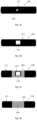
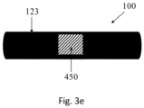
Fig. 3a-3e is a side view of a first embodiment of the repair procedure. -
Fig. 4a-4f is a side view of a second embodiment of the repair procedure. - The electric properties of a cable are dependent, amongst other things, on the properties of the insulation system that surrounds the electric conductor. Failure of the insulation system will lead to failure of the cable, which will then need to be repaired, a costly and time-consuming operation.
- A typical insulation system comprises an inner semiconducting layer, an insulating layer and an outer semiconducting layer.
- Defects, such as damages or pollutants can appear on the outer semiconducting layer of a cable during production or in the field during installation. If such defects are left unchecked, they may impact the performance of the cable, and will possibly ultimately lead to cable failure.
- The current invention relates to a method for repairing the outer semiconducting layer of a cable.
- As illustrated in
fig. 1 , a typicalelectric cable 100 comprises anelectric conductor 110, and an insulation system 120 surrounding theelectric conductor 110. The insulation system 120 comprises an innersemiconducting layer 121, an insulatinglayer 122 and an outersemiconducting layer 123. Theelectric cable 100 may further comprise awater barrier layer 130 surrounding the insulation system 120. Theelectric cable 100 may further comprise apolymeric sheath 140, surrounding the insulation system 120 or surrounding the insulation system 120 and thewater barrier layer 130. - In the cable to be repaired, a section of the outer
semiconducting layer 123 comprises adefect 200, as illustrated infig.3a and4a . - The inventive method comprises the steps of
- a) Laying a
non-stick sheet 300 comprising acutout window 350 on thecable 100 so that thecutout window 350 surrounds the section originally comprising thedefect 200, as illustrated infig.3c and4c . -
Figure 2 illustrates anon-stick sheet 300 with acutout window 350. An advantage of the inventive method is that the size and shape of thenon-stick sheet 300 and of thecutout window 350 can be adapted to thedefect 200 and/or section of the outersemiconducting layer 123 to be repaired. - The
non-stick sheet 300 may for example comprise a Teflon layer (or even be a Teflon sheet), a polyimide layer (e.g. a Kapton layer), paper (e.g. baking paper), a wood layer, a metal layer, a silicone layer, a glass or glass fiber layer, or a ceramic layer. - Depending on the type of defect, it is not always necessary to remove the affected area. These defects may for example be holes, tears, buckling, overgrowth, cuts, scratches, imprints, scorch, poor plasticization, impurities etc.
- The next step in the method comprises
b) Applying asemiconductive material 400 at least over thecutout window 350 and at most over thenon-stick sheet 300, as illustrated infig.3d and4d . - Here the intention is that the
semiconductive material 400 replaces the material in the section comprising thedefect 200. Thereafter, the method comprises
c) Bonding thesemiconductive material 400 to thecable 100. - The bonding may for example be achieved by heating the semiconducting material over its melting point. This step is followed by
d) Removing thenon-stick sheet 300 and any unbound parts of the semiconductive material, as illustrated infig.3e and4e . Thesemiconductive material 450 is maintained on the repaired cable. - The method may further include the step of:
e) stripping the section of outersemiconducting layer 123 comprising thedefect 200 before applying thesemiconductive material 400 in step b), as illustrated infig.3b and4b . - An advantage of the inventive method is that one does not necessarily need to remove the full thickness of the outer semiconducting layer.
- Another advantage of the inventive method is that one does not necessarily need to remove a complete cylindrical section of the outer semiconducting layer to repair it, but that the section can for example be a cylindrical sector containing the
defect 200. When a cylindrical sector is removed the non-stick sheet is adapted to form a cylindrical cutout window. - However, in some cases, the section of the outer
semiconducting layer 123 comprising thedefect 200 may preferably stripped down to the insulatinglayer 122, for example in order to ensure that the defect does not also affect the insulatinglayer 122. - The method may further include the step of:
f) sanding the repaired outersemiconducting layer 123, as illustrated infig.4f . - Step f) is performed after step d). An advantage of this step is that it allows control over the final diameter and the surface quality of the repaired outer
semiconducting layer 123/450. - The
electric cable 100 may further comprise awater barrier layer 130, surrounding the insulation system 120 and the method may further comprise the step of restoring thewater barrier layer 130. - The
electric cable 100 may further comprise apolymeric sheath 140, surrounding the insulation system 120 or surrounding the insulation system 120 and thewater barrier layer 130 and the method may further comprise the step of restoring thepolymeric sheath 140. - In a first example, after identifying a defect on an electric cable, the electric cable comprising an electric conductor, and an insulation system surrounding the electric conductor; wherein the insulation system comprises an inner semiconducting layer, an insulating layer and an outer semiconducting layer; the operator laid a non-stick sheet, here a Teflon foil, comprising a cutout window on the cable so that the cutout window surrounded the section comprising the defect. The operator then removed the visible defect with a knife making sure no more defect was visible. The operator thereafter applied a semiconductive tape of the same material as the outer semiconducting layer of the electric cable, over the cutout window and part of the non-stick sheet. The operator then wrapped the semiconducting tape and the cable with a non-adhesive tape, applying pressure on the tape to be bonded, for example here, a non-adhesive tape with a melting point over the temperature at which the semiconductive material will be heated. The operator then heated the semiconductive tape, by using heating cables, warming the semiconducting tape up to 240 °C in approximately 1 hour, then kept the temperature at 240 °C during 45min. The semiconducting tape was then allowed to cool down to room temperature, for approximately 15min. If desirable, the section being repaired may alternatively be actively cooled. The operator then removed any unbound parts of the semiconductive tape, and sanded the surface of the cable in the section originally comprising the defect, thus providing a repaired outer semiconducting layer.
- In this example, the electric properties of the repaired semi-conducting layer were tested and the repaired semi-conducting layer had electrical properties equivalent to portions of the cables having no defects.
Claims (14)
- A method for repairing an electric cable (100), the electric cable (100) comprising an electric conductor (110), and an insulation system (120) surrounding the electric conductor (110); wherein the insulation system (120) comprises an inner semiconducting layer (121), an insulating layer (122) and an outer semiconducting layer (123),wherein a section of the outer semiconducting layer (123) comprises a defect (200);the method comprising the steps ofa) laying a non-stick sheet (300) comprising a cutout window (350) on the cable (100) so that the cutout window (350) surrounds the section comprising the defect;b) applying semiconductive material (400) at least over the cutout window (350) and at most over the non-stick sheet (300);c) bonding the semiconductive material (400) to the cable (100); andd) removing any unbound parts of the semiconductive material providing a repaired outer semiconducting layer.
- The method according to claim 1 wherein step c) of bonding the semiconductive material (400) is achieved by heating.
- The method according to claim 2, wherein the semiconductive material (400) is heated between 70 and 500°C during step c).
- The method according to any one of claims 2 to 3, wherein the semiconductive material (400) is heated at a speed of at least 20°C/h during step c).
- The method according to any of the previous claims, wherein the semiconductive material (400) is in the form of a tape of semiconductive material (400).
- The method according to claim 1 comprising the step of:
e) stripping the section of outer semiconducting layer (123) comprising the defect (200) before applying the semiconductive material (400) in step b). - The method according to claim 6 wherein the section of the outer semiconducting layer (123) comprising the defect (200) is stripped down to the insulating layer (122).
- The method according to any of the previous claims, further including the step of:
f) sanding the repaired outer semiconducting layer (123), after step d). - The method according to any of the previous claims, wherein the non-stick sheet comprises a Teflon layer.
- The method according to any of the previous claims, wherein the outer semiconducting layer (123) has a diameter after the repair that is at most 120% the diameter of the semiconducting layer (123) before the repair.
- The method according to any of the previous claims, wherein the outer semiconducting layer (123) has a diameter after the repair that is at most equal to the diameter of the semiconducting layer (123) before the repair.
- The method according to any of the previous claims, wherein the electric cable (100) further comprises a water barrier layer (130), surrounding the insulation system (120) and the method further comprises the step of restoring the water barrier layer (130).
- The method according to any of the previous claims, wherein the electric cable further comprises a polymeric sheath (140), surrounding the insulation system (120) or surrounding the insulation system (120) and the water barrier layer (130) and the method further comprises the step of restoring the polymeric sheath (140).
- An electric cable comprising a semiconducting layer (123) repaired by the method according to any one of the claims 1 to 13.
Priority Applications (1)
| Application Number | Priority Date | Filing Date | Title |
|---|---|---|---|
| EP22306874.3A EP4387021A1 (en) | 2022-12-14 | 2022-12-14 | Method for repairing a cable outer semiconducting layer |
Applications Claiming Priority (1)
| Application Number | Priority Date | Filing Date | Title |
|---|---|---|---|
| EP22306874.3A EP4387021A1 (en) | 2022-12-14 | 2022-12-14 | Method for repairing a cable outer semiconducting layer |
Publications (1)
| Publication Number | Publication Date |
|---|---|
| EP4387021A1 true EP4387021A1 (en) | 2024-06-19 |
Family
ID=84602637
Family Applications (1)
| Application Number | Title | Priority Date | Filing Date |
|---|---|---|---|
| EP22306874.3A Pending EP4387021A1 (en) | 2022-12-14 | 2022-12-14 | Method for repairing a cable outer semiconducting layer |
Country Status (1)
| Country | Link |
|---|---|
| EP (1) | EP4387021A1 (en) |
Citations (5)
| Publication number | Priority date | Publication date | Assignee | Title |
|---|---|---|---|---|
| JPH10304528A (en) * | 1997-04-24 | 1998-11-13 | Yazaki Corp | Wire and cable repair method |
| CN101741031A (en) | 2009-12-23 | 2010-06-16 | 上海德力西集团有限公司 | Application of semi-conductive adhesive for repairing semi-conductive shield outside medium-voltage cross-linked cable |
| CN103701073A (en) * | 2013-12-27 | 2014-04-02 | 浙江造船有限公司 | Method for repairing thermoplastic sheath cable |
| CN110601097A (en) * | 2018-09-30 | 2019-12-20 | 西南交通大学 | Universal repair method for cable damage |
| CN113488928A (en) * | 2021-08-08 | 2021-10-08 | 南京中车浦镇城轨车辆有限责任公司 | Cable repairing method for rail transit vehicle |
-
2022
- 2022-12-14 EP EP22306874.3A patent/EP4387021A1/en active Pending
Patent Citations (5)
| Publication number | Priority date | Publication date | Assignee | Title |
|---|---|---|---|---|
| JPH10304528A (en) * | 1997-04-24 | 1998-11-13 | Yazaki Corp | Wire and cable repair method |
| CN101741031A (en) | 2009-12-23 | 2010-06-16 | 上海德力西集团有限公司 | Application of semi-conductive adhesive for repairing semi-conductive shield outside medium-voltage cross-linked cable |
| CN103701073A (en) * | 2013-12-27 | 2014-04-02 | 浙江造船有限公司 | Method for repairing thermoplastic sheath cable |
| CN110601097A (en) * | 2018-09-30 | 2019-12-20 | 西南交通大学 | Universal repair method for cable damage |
| CN113488928A (en) * | 2021-08-08 | 2021-10-08 | 南京中车浦镇城轨车辆有限责任公司 | Cable repairing method for rail transit vehicle |
Similar Documents
| Publication | Publication Date | Title |
|---|---|---|
| CA1268831A (en) | Electrical cable splice enclosure | |
| CN106655019A (en) | Improved process for cold-shrink installation of 10-35KV cable intermediate joint | |
| US9545743B2 (en) | Readily strippable cable | |
| CN106451256A (en) | Improved cold-contraction installation process for cable intermediate joint | |
| EP3320588B1 (en) | A method of building an insulation system around a naked conductor section of a power cable | |
| US11508495B2 (en) | Method of preparing epoxy coated bus bars for use in electrical distribution equipment | |
| CN119340873B (en) | 35KV and below polypropylene cable terminal manufacturing method and polypropylene cable terminal | |
| US11277058B2 (en) | Repair method for bar or coil of rotating electrical machine | |
| US4446095A (en) | Method for manufacturing heat shrinkable tubing | |
| US12633433B2 (en) | Heating assembly and method for insulation system restoration of a power cable | |
| EP0886342A1 (en) | Cable joint | |
| US20220415542A1 (en) | Pressurisation and Heating Device and Method for Insulation System Restoration of a Power Cable | |
| CN111092395B (en) | Fusion type cold-shrink intermediate joint and installation method of cold-shrink terminal | |
| US4519759A (en) | Apparatus for making shrinkable tubing | |
| US3474517A (en) | Method and apparatus for preparing cross - linked polyethylene cables for terminations and splices | |
| JP3243142B2 (en) | Method of forming prefabricated connection of crosslinked polyethylene insulated power cable | |
| JPH05266958A (en) | Method for manufacturing power cable connection | |
| JP4309077B2 (en) | CV cable mold heating tube and CV cable terminal processing method. | |
| JP2596275B2 (en) | How to assemble the power cable connection | |
| CN121149758A (en) | Production method of connector assembly and connector assembly | |
| JPH04368411A (en) | Method of processing terminal tip for testing of power cable | |
| CN114083726A (en) | Inner semi-conducting layer cross-linking forming device and cross-linking forming process | |
| JPH0648886B2 (en) | Surface shaping method for plastic cables | |
| JPH0232753B2 (en) | GOMU * PURASUCHITSUKUZETSUENKEEBURUNOSETSUZOKUHOHO | |
| JPH09284943A (en) | Method for extrusion mold joint of bridgeable polyethylene cable |
Legal Events
| Date | Code | Title | Description |
|---|---|---|---|
| PUAI | Public reference made under article 153(3) epc to a published international application that has entered the european phase |
Free format text: ORIGINAL CODE: 0009012 |
|
| STAA | Information on the status of an ep patent application or granted ep patent |
Free format text: STATUS: THE APPLICATION HAS BEEN PUBLISHED |
|
| AK | Designated contracting states |
Kind code of ref document: A1 Designated state(s): AL AT BE BG CH CY CZ DE DK EE ES FI FR GB GR HR HU IE IS IT LI LT LU LV MC ME MK MT NL NO PL PT RO RS SE SI SK SM TR |
|
| STAA | Information on the status of an ep patent application or granted ep patent |
Free format text: STATUS: REQUEST FOR EXAMINATION WAS MADE |
|
| 17P | Request for examination filed |
Effective date: 20241219 |