EP4386113A1 - Electrical terminal with metal conductive layer comprising silver - Google Patents
Electrical terminal with metal conductive layer comprising silver Download PDFInfo
- Publication number
- EP4386113A1 EP4386113A1 EP22213244.1A EP22213244A EP4386113A1 EP 4386113 A1 EP4386113 A1 EP 4386113A1 EP 22213244 A EP22213244 A EP 22213244A EP 4386113 A1 EP4386113 A1 EP 4386113A1
- Authority
- EP
- European Patent Office
- Prior art keywords
- layer
- silver
- indium
- gallium
- tin
- Prior art date
- Legal status (The legal status is an assumption and is not a legal conclusion. Google has not performed a legal analysis and makes no representation as to the accuracy of the status listed.)
- Pending
Links
Images

Classifications
-
- H—ELECTRICITY
- H01—ELECTRIC ELEMENTS
- H01R—ELECTRICALLY-CONDUCTIVE CONNECTIONS; STRUCTURAL ASSOCIATIONS OF A PLURALITY OF MUTUALLY-INSULATED ELECTRICAL CONNECTING ELEMENTS; COUPLING DEVICES; CURRENT COLLECTORS
- H01R13/00—Details of coupling devices of the kinds covered by groups H01R12/70 or H01R24/00 - H01R33/00
- H01R13/02—Contact members
- H01R13/03—Contact members characterised by the material, e.g. plating, or coating materials
-
- C—CHEMISTRY; METALLURGY
- C25—ELECTROLYTIC OR ELECTROPHORETIC PROCESSES; APPARATUS THEREFOR
- C25D—PROCESSES FOR THE ELECTROLYTIC OR ELECTROPHORETIC PRODUCTION OF COATINGS; ELECTROFORMING; APPARATUS THEREFOR
- C25D5/00—Electroplating characterised by the process; Pretreatment or after-treatment of workpieces
- C25D5/10—Electroplating with more than one layer of the same or of different metals
-
- C—CHEMISTRY; METALLURGY
- C25—ELECTROLYTIC OR ELECTROPHORETIC PROCESSES; APPARATUS THEREFOR
- C25D—PROCESSES FOR THE ELECTROLYTIC OR ELECTROPHORETIC PRODUCTION OF COATINGS; ELECTROFORMING; APPARATUS THEREFOR
- C25D5/00—Electroplating characterised by the process; Pretreatment or after-treatment of workpieces
- C25D5/10—Electroplating with more than one layer of the same or of different metals
- C25D5/12—Electroplating with more than one layer of the same or of different metals at least one layer being of nickel or chromium
-
- C—CHEMISTRY; METALLURGY
- C25—ELECTROLYTIC OR ELECTROPHORETIC PROCESSES; APPARATUS THEREFOR
- C25D—PROCESSES FOR THE ELECTROLYTIC OR ELECTROPHORETIC PRODUCTION OF COATINGS; ELECTROFORMING; APPARATUS THEREFOR
- C25D5/00—Electroplating characterised by the process; Pretreatment or after-treatment of workpieces
- C25D5/48—After-treatment of electroplated surfaces
- C25D5/50—After-treatment of electroplated surfaces by heat-treatment
-
- C—CHEMISTRY; METALLURGY
- C25—ELECTROLYTIC OR ELECTROPHORETIC PROCESSES; APPARATUS THEREFOR
- C25D—PROCESSES FOR THE ELECTROLYTIC OR ELECTROPHORETIC PRODUCTION OF COATINGS; ELECTROFORMING; APPARATUS THEREFOR
- C25D7/00—Electroplating characterised by the article coated
-
- H—ELECTRICITY
- H01—ELECTRIC ELEMENTS
- H01R—ELECTRICALLY-CONDUCTIVE CONNECTIONS; STRUCTURAL ASSOCIATIONS OF A PLURALITY OF MUTUALLY-INSULATED ELECTRICAL CONNECTING ELEMENTS; COUPLING DEVICES; CURRENT COLLECTORS
- H01R13/00—Details of coupling devices of the kinds covered by groups H01R12/70 or H01R24/00 - H01R33/00
- H01R13/02—Contact members
-
- H—ELECTRICITY
- H01—ELECTRIC ELEMENTS
- H01R—ELECTRICALLY-CONDUCTIVE CONNECTIONS; STRUCTURAL ASSOCIATIONS OF A PLURALITY OF MUTUALLY-INSULATED ELECTRICAL CONNECTING ELEMENTS; COUPLING DEVICES; CURRENT COLLECTORS
- H01R13/00—Details of coupling devices of the kinds covered by groups H01R12/70 or H01R24/00 - H01R33/00
- H01R13/02—Contact members
- H01R13/10—Sockets for co-operation with pins or blades
- H01R13/11—Resilient sockets
Definitions
- the present invention relates to an electrical terminal and in particular, to an electrical terminal with a metal conductive layer comprising silver.
- Electrical connectors are typically formed from a base substrate material that is coated with a high electrical-conductivity layer to enable contacts to be mated with minimised contact resistance.
- Example electrical contacts include conductive pins insertable within backplates and male and female push-fit contacts to couple electronic components and/or circuits.
- Typical electrically conducting plating materials include copper, gold, nickel, silver, tin and alloys thereof.
- Silver as a contact plating provides high conductivity and ductility to allow the connectors to compress together when mated. This maximises the contact area and minimises contact resistance. Silver is also easy to solder. However, silver connectors, unlike other metals such as gold, tends to tarnish in air. Other plating materials may oxidise or can be susceptible to environmental degradation that may affect the conductivity, connection interface or integrity. Accordingly, in a process known as passivation, protective films or layers can be provided over the conducting layer to prevent corrosion and/or wear.
- the electrical connector may be a male or female electrical terminal. It is a further specific objective to provide a process for manufacturing the electrical terminal.
- an electrical terminal comprising a substrate and a metallic conductive layer provided on the substrate.
- the electrical terminal may be a male or female electrical terminal.
- the metallic conductive layer comprises either:
- the intermetallic phase may comprise elemental compounds, such as compounds of silver and indium or gallium or a mixture thereof.
- the intermetallic phase may comprise a mixture of two or more elements, for example, silver and indium or gallium or mixture thereof.
- the intermetallic phase or the bismuth layer protects the silver layer in the metallic conductive layer from environmental effects, wear and tarnishing. Further, the insertion forces required for the terminal are reduced due to the presence of the intermetallic phase. Additionally, a terminal is provided having a more stable insertion force. Such effects provide a terminal with enhanced longevity relative to existing terminals and that may be manufactured via convenient and raw material efficient processes.
- the intermetallic phase comprises tin.
- the concentration of indium, gallium or tin in the intermetallic phase increases in a direction extending away from the substrate.
- the intermetallic phase may include various intermetallic compounds; for example, AgIn 2 , Ag 2 In, Ag 3 Sn, Ag 2 Ga, or Ag 3 Ga 2 .
- the intermetallic phase comprises indium and a wt% predominant intermetallic compound in the intermetallic phase is AgIn 2 ; or the intermetallic phase comprises gallium and a wt% predominant intermetallic compound in the intermetallic phase is Ag 3 Ga 2 ; and/or Ag 2 Ga; or the intermetallic phase comprises tin and a wt% predominant intermetallic compound in the intermetallic phase is Ag 3 Sn.
- the metallic conductive layer may comprise bismuth and silver and/or a silver-bismuth compound or alloy.
- the terminal further comprises a barrier layer between the substrate and the silver layer.
- the barrier layer prevents diffusion of the silver into the substrate.
- the barrier layer may comprise any one or a combination of the group comprising: nickel, copper or aluminium or alloys thereof.
- the barrier layer may comprise nickel.
- the terminal further comprises a silver layer.
- the silver layer comprises at least 50%, 60%, 70%, 80%, 90%, 95%, 97%, or 99% silver.
- the terminal comprises a layer of any one or a combination of the group comprising: indium, gallium, bismuth or tin comprising at least 50%, 60%, 70%, 80%, 90%, 95%, 97%, or 99% of any of indium, gallium, bismuth or tin.
- the terminal comprising both a silver layer comprising at least 50%, 60%, 70%, 80%, 90%, 95%, 97%, or 99% of silver and a layer of any one or a combination of the group comprising: indium, gallium, bismuth or tin comprising at least 50%, 60%, 70%, 80%, 90%, 95%, 97%, or 99% of any of indium, gallium, bismuth or tin.
- the layer of any one or a combination of the group comprising: indium, gallium or tin is disposed directly on the intermetallic phase.
- the intermetallic phase is disposed directly on the silver layer.
- the silver layer is disposed directly on the barrier layer.
- the barrier layer is disposed directly on the substrate.
- the process comprises the step of tempering or storing the terminal to form an intermetallic phase comprising silver and any one or a combination of the group comprising: indium, gallium or tin.
- the process may include a tempering step, storing step, or both a tempering and storing step.
- a tempering step During tempering and storing, the thickness of the intermetallic phase increases, and consequently the thickness of the silver layer and the layer of any one or a combination of the group comprising: indium, gallium or tin decreases.
- the silver is deposited to a thickness of between 0.5 and 10 ⁇ m, 2 and 6 ⁇ m, or 4 and 5 ⁇ m.
- the indium, gallium, bismuth or tin or combination thereof is deposited to a thickness of between 0.1 and 5 ⁇ m, 0.3 and 2 ⁇ m, or 0.5 and 1 ⁇ m.
- the terminal is tempered by heating to a temperature within 50°C below the melting point of the indium, gallium, bismuth or tin. Preferably, the terminal is tempered by heating for between 5 seconds and 5 minutes.
- the terminal is stored for between 2 hours and 7 days after the indium, gallium, bismuth, tin or combination thereof is deposited.
- the process comprises initially forming a barrier layer on the substrate before depositing the silver and thereafter depositing the silver on the barrier layer.
- the barrier layer may be formed by depositing any one of or a combination of the group comprising: nickel, copper, aluminium or alloys thereof.
- the barrier layer may be deposited to a thickness of between 0.1 and 10 ⁇ m, 0.5 and 3 ⁇ m, or 1 and 2 ⁇ m.
- each terminal 2, 4 comprises a metallic body, defining a substrate 6.
- the substrate 6 is formed from copper alloy, but alternative metals may be used such as aluminium alloy.
- Each terminal 2, 4 further has a metallic conductive layer 8 provided on the substrate 6.
- the metallic conductive layer 8 has an intermetallic phase 10 of silver and indium.
- the intermetallic phase may be formed of silver and any other suitable chemical.
- suitable chemicals include the post-transition metals gallium or tin.
- indium protects the silver in the conductive layer 8 from environmental effects, wear and tarnishing. Further, as indium is softer than silver, the necessary insertion force for the terminals 2, 4 is reduced in the present invention when compared with terminals with pure silver conductive layers.
- the intermetallic phase may contain a plurality of elements other than silver, for example, a combination of any of indium, gallium or tin.
- the predominant wt% intermetallic compound in the intermetallic phase is AgIn 2 .
- the predominant compound can be controlled depending on the conditions of formation of the intermetallic phase.
- Other compounds may also be present, such as Ag 2 In.
- the predominant compound may be Ag 3 Ga 2 respectively.
- other compounds of silver-bismuth or silver-gallium may be present.
- the concentration of indium in the intermetallic phase 10 increases in a direction heading away from the substrate 6.
- the concentration of indium is lowest at a location close to the substrate 6 and highest at a location furthest away from the substrate 6.
- the concentration of silver in the intermetallic phase decreases in a direction heading away from the substrate 6. The concentration of silver therefore is greatest at a location close to the substrate 6 and lowest at a location furthest away from the substrate.
- gallium or tin may be used in place of indium, or alongside indium, the concentration of these elements will again be lowest close to the substrate and highest further from the substrate.
- the terminals 2, 4 each comprise a barrier layer 12 located between the substrate 6 and the intermetallic phase 10.
- the barrier layer 12 prevents diffusion of the silver into the substrate.
- the barrier layer 12 is formed from nickel, but alternative materials may be used such as copper, aluminium, or alloys thereof.
- the thickness of the barrier layer 12 is preferably between 1 and 2 ⁇ m, but may alternatively be between 0.5 and 3 ⁇ m or 0.1 and 10 ⁇ m.
- the terminals 2, 4 further have a silver layer 14.
- the metallic conductive layer 8 comprises a bismuth layer arranged on the silver layer.
- the silver layer 14 is located between the substrate 6 and intermetallic phase 10, or between the substrate and the bismuth layer. More specifically, the silver layer 14 is located between the barrier layer 12 and the intermetallic phase 10 or bismuth layer.
- the terminals 2, 4 further have an indium layer 16.
- the indium layer is the outermost layer of the metallic conductive layer 8.
- the intermetallic phase 10 is located between the indium layer 16 and silver layer 14, barrier layer 12 and substrate 6.
- the indium layer has a thickness of up to 5 ⁇ m.
- the outermost layer may be a gallium, bismuth or tin layer, or combinations thereof, possibly also with indium.
- the indium layer 16 which may also be formed from any of gallium, bismuth or tin or combination thereof, has a top surface 16a, and bottom surface 16b wherein the top surface 16a is at one side of the layer and the bottom surface 16b is at an opposing side.
- the intermetallic phase 10 further has a top surface 10a and a bottom surface 10b wherein the top surface 10a is at one side of the layer and the bottom surface 10b is at an opposing side.
- the bottom surface 16b of the indium layer 16 is in contact with the top surface 10a of the intermetallic phase 10.
- the top surface 16a of the indium layer is ideally exposed and represents the outermost surface of the conductive layer 8.
- the silver layer 14 further has a top surface 14a and a bottom surface 14b wherein the top surface 14a is at one side of the layer and the bottom surface 14b is at an opposing side.
- the bottom surface 10b of the intermetallic phase is in contact with the top surface 14a of the silver layer.
- the barrier layer 12 further has a top surface 12a and a bottom surface 12b wherein the top surface 12a is at one side of the layer and the bottom surface 12b is at an opposing side.
- the bottom surface 14b of the silver layer is in contact with the top surface 12a of the barrier layer.
- the substrate 6 has a top layer 6a.
- the top layer 6a of the substrate 6 is in contact with the bottom surface 12b of the barrier layer.
- the male electrical terminal 2 is inserted into the female electrical terminal 4.
- the metallic conductive layers 8 of each of the male and female electrical terminals 2, 4 then contact one another and electric current can then flow between the terminals 2, 4.
- Such terminals 2, 4 may be connected to electrical cables via crimping or ultrasonic welding.
- the electrical cables may be copper or aluminium cables.
- the terminals 2, 4 may be housed in a connector housing and joined to the electrical cables for connection with other related electrical equipment.
- the terminals of the present invention can be formed by reel-to-reel plating.
- reel-to-reel plating strips of material or plated and then formed into the desired product.
- Immersion plating is typically used for depositing large quantities of metals, whereas spot technique offers higher selectivity to save metal quantity.
- rolled blank material or pre-stamped material is de-reeled and will be fed through multiple process including rinsing, plating and drying, before being rewound onto a new real after having been plated.
- the terminals of the present invention can be formed by an electro-plating process.
- electro-plating the substrate is placed into an electrolyte solution in an electrolysis bath.
- An anode is present in the electrolyte solution which comprises the desired coating material.
- the substrate is the cathode.
- the transfer of the material from the cathode is achieved by setting the electrolysis parameters such as bath temperature, pH, voltage, current, electrolyte concentration and rinsing steps. The skilled person will understand that many combinations of parameters exist that will achieve the adequate plating thickness and metal quality.
- the terminals 2, 4 are formed according to the following method. Initially, the substrate 6 is provided. Next, the barrier layer 12 is formed by depositing nickel on the substrate 6 to a thickness of 1-2 ⁇ m. Alternatively, the nickel may be deposited to a thickness of 0.5-3 ⁇ m or 0.1-10 ⁇ m. Further alternatively, the barrier layer may be formed by depositing any one of or a combination of the group comprising: nickel, copper, aluminium or alloys thereof.
- silver 14 is deposited indirectly on the substrate 6 to form a silver layer.
- directly we mean the silver is deposited on the barrier layer 12 which in turn is deposited on the substrate 6.
- the silver 14 may be deposited directly on the substrate 6.
- the silver 14 is deposited to a thickness of between 4 and 5 ⁇ m.
- the silver 14 may be deposited to a thickness of between 0.5 and 10 ⁇ m or 2 and 6 ⁇ m.
- indium 16 is deposited on the silver layer 14 to form an indium layer 16.
- the indium 16 is deposited to a thickness of between 0.5 and 1 ⁇ m but may be deposited to thicknesses of between 0.1 and 5 ⁇ m, 0.3 and 2 ⁇ m.
- gallium, bismuth or tin may be deposited rather than indium, or combinations of any of indium, gallium, bismuth or tin.
- the bottom surface 16b of the indium layer 16 is in contact with the top surface 14a of the silver layer; the bottom surface 14b of the silver layer is in contact with the top surface 12a of the barrier layer, and; the top layer 6a of the substrate 6 is in contact with the bottom surface 12b of the barrier layer.
- the terminals 2, 4 are then processed to form the intermetallic phase 10.
- the intermetallic phase 10 is formed by preferably tempering 16 and then storing 18 the terminals 2, 4.
- the intermetallic phase 10 may be also be formed by either a tempering step 16 or storage step 18 alone.
- the thickness of the intermetallic phase 10 increases, and consequently the thickness of the silver layer 14 and indium layer 16 decreases.
- the thickness of the indium, gallium or tin layers should be at least 50% of the initial thickness (i.e., the thickness before tempering).
- the indium may deposited to a thickness of between 0.3 and 2 ⁇ m.
- the indium layer should have a thickness of between 0.15 and 2 ⁇ m.
- the tempering step 16 involves heating the terminal 2, 4 to a temperature within 50°C below the melting point of indium. Ideally, the terminal 2, 4 is heated to just below the melting point of indium, for example 140-150°C. Where metals other than indium are used, the heating temperature should be altered accordingly to below the melting point of the alternative metal. The heated temperature is maintained for 30 seconds, but shorter or longer periods may also be used and a range of between 5 seconds and 5 minutes may be suitable.
- the terminal 2, 4 is simply stored, preferably at ambient temperature, for a period of time to allow the intermetallic phase 10 to form. Ideally, the terminal 2, 4 is stored for 1-3 days but shorter or longer time periods may also be acceptable, for example between 2 hours and 7 days.
Landscapes
- Chemical & Material Sciences (AREA)
- Engineering & Computer Science (AREA)
- Chemical Kinetics & Catalysis (AREA)
- Electrochemistry (AREA)
- Materials Engineering (AREA)
- Metallurgy (AREA)
- Organic Chemistry (AREA)
- Non-Insulated Conductors (AREA)
Abstract
Description
- The present invention relates to an electrical terminal and in particular, to an electrical terminal with a metal conductive layer comprising silver.
- Electrical connectors are typically formed from a base substrate material that is coated with a high electrical-conductivity layer to enable contacts to be mated with minimised contact resistance. Example electrical contacts include conductive pins insertable within backplates and male and female push-fit contacts to couple electronic components and/or circuits. Typical electrically conducting plating materials include copper, gold, nickel, silver, tin and alloys thereof.
- Silver as a contact plating provides high conductivity and ductility to allow the connectors to compress together when mated. This maximises the contact area and minimises contact resistance. Silver is also easy to solder. However, silver connectors, unlike other metals such as gold, tends to tarnish in air. Other plating materials may oxidise or can be susceptible to environmental degradation that may affect the conductivity, connection interface or integrity. Accordingly, in a process known as passivation, protective films or layers can be provided over the conducting layer to prevent corrosion and/or wear.
- Difficulties exist in ensuring that the passivation process is consistent, and this results in variations in the protective properties of the passivation layer in the final product. Therefore, there is a desire for silver-containing terminals that do not require passivation. One known solution is to provide silver alloys (for example Ag-C, Ag-W or Ag-Cu) on a substrate. However, this too presents problems because the concentration of the element stoichiometry of the silver alloys is difficult to specify, produce and control. Thus, what is required is improved electrical connectors and contacts that do not require passivation and which are simpler to manufacture than the said known solutions.
- It is known to use soft metals, such as indium or bismuth, in electrical connections, with the purpose of reducing the insertion forces and to reduce PCB damage during the connection process. Further, it is also known that silver may form an intermetallic phase with indium, gallium or tin.
- It is an objective of the present disclosure to provide an electrical connector having high electrical conductivity, low contact resistance as well as a resistance to environmental effects, wear and tarnishing. It is a further specific objective to provide a silver-based electrical connector that has an improved or simplified manufacturing process. The electrical connector may be a male or female electrical terminal. It is a further specific objective to provide a process for manufacturing the electrical terminal.
- According to a first aspect of the present disclosure there is provided an electrical terminal comprising a substrate and a metallic conductive layer provided on the substrate. The electrical terminal may be a male or female electrical terminal. The metallic conductive layer comprises either:
- a silver layer and an intermetallic phase of silver and one or a combination of indium or gallium, or;
- a silver layer and a bismuth layer, wherein the silver layer is located between the substrate and the bismuth layer.
- The intermetallic phase may comprise elemental compounds, such as compounds of silver and indium or gallium or a mixture thereof. In addition, or alternatively the intermetallic phase may comprise a mixture of two or more elements, for example, silver and indium or gallium or mixture thereof.
- The intermetallic phase or the bismuth layer protects the silver layer in the metallic conductive layer from environmental effects, wear and tarnishing. Further, the insertion forces required for the terminal are reduced due to the presence of the intermetallic phase. Additionally, a terminal is provided having a more stable insertion force. Such effects provide a terminal with enhanced longevity relative to existing terminals and that may be manufactured via convenient and raw material efficient processes.
- In an embodiment, the intermetallic phase comprises tin. Preferably, the concentration of indium, gallium or tin in the intermetallic phase increases in a direction extending away from the substrate.
- The intermetallic phase may include various intermetallic compounds; for example, AgIn2, Ag2In, Ag3Sn, Ag2Ga, or Ag3Ga2. Optionally, the intermetallic phase comprises indium and a wt% predominant intermetallic compound in the intermetallic phase is AgIn2; or the intermetallic phase comprises gallium and a wt% predominant intermetallic compound in the intermetallic phase is Ag3Ga2; and/or Ag2Ga; or the intermetallic phase comprises tin and a wt% predominant intermetallic compound in the intermetallic phase is Ag3Sn. The metallic conductive layer may comprise bismuth and silver and/or a silver-bismuth compound or alloy.
- Ideally, the terminal further comprises a barrier layer between the substrate and the silver layer. The barrier layer prevents diffusion of the silver into the substrate. The barrier layer may comprise any one or a combination of the group comprising: nickel, copper or aluminium or alloys thereof. In an embodiment where the substrate comprises copper, the barrier layer may comprise nickel.
- Optionally, the terminal further comprises a silver layer. Ideally, the silver layer comprises at least 50%, 60%, 70%, 80%, 90%, 95%, 97%, or 99% silver. Yet further optionally, the terminal comprises a layer of any one or a combination of the group comprising: indium, gallium, bismuth or tin comprising at least 50%, 60%, 70%, 80%, 90%, 95%, 97%, or 99% of any of indium, gallium, bismuth or tin. Alternatively, the terminal comprising both a silver layer comprising at least 50%, 60%, 70%, 80%, 90%, 95%, 97%, or 99% of silver and a layer of any one or a combination of the group comprising: indium, gallium, bismuth or tin comprising at least 50%, 60%, 70%, 80%, 90%, 95%, 97%, or 99% of any of indium, gallium, bismuth or tin.
- Ideally, the layer of any one or a combination of the group comprising: indium, gallium or tin is disposed directly on the intermetallic phase. Further ideally, the intermetallic phase is disposed directly on the silver layer. Optionally, the silver layer is disposed directly on the barrier layer. Optionally the barrier layer is disposed directly on the substrate.
- According to a second aspect of the invention there is provided a process for manufacturing the terminal of first aspect of the invention, the process comprising the steps of:
- depositing silver directly or indirectly on a substrate to form a silver layer;
- depositing any one or a combination of the group comprising: indium, gallium, bismuth or tin on the silver layer, to form a layer of any one or a combination of the group comprising: indium, gallium, bismuth or tin.
- Ideally, the process comprises the step of tempering or storing the terminal to form an intermetallic phase comprising silver and any one or a combination of the group comprising: indium, gallium or tin.
- The process may include a tempering step, storing step, or both a tempering and storing step. During tempering and storing, the thickness of the intermetallic phase increases, and consequently the thickness of the silver layer and the layer of any one or a combination of the group comprising: indium, gallium or tin decreases.
- Ideally, the silver is deposited to a thickness of between 0.5 and 10 µm, 2 and 6 µm, or 4 and 5 µm.
- Preferably, the indium, gallium, bismuth or tin or combination thereof is deposited to a thickness of between 0.1 and 5 µm, 0.3 and 2 µm, or 0.5 and 1 µm.
- Ideally, the terminal is tempered by heating to a temperature within 50°C below the melting point of the indium, gallium, bismuth or tin. Preferably, the terminal is tempered by heating for between 5 seconds and 5 minutes.
- Optionally, the terminal is stored for between 2 hours and 7 days after the indium, gallium, bismuth, tin or combination thereof is deposited.
- Ideally, the process comprises initially forming a barrier layer on the substrate before depositing the silver and thereafter depositing the silver on the barrier layer. The barrier layer may be formed by depositing any one of or a combination of the group comprising: nickel, copper, aluminium or alloys thereof.
- The barrier layer may be deposited to a thickness of between 0.1 and 10 µm, 0.5 and 3 µm, or 1 and 2 µm.
- A specific implementation of the present disclosure will now be described, by way of example only, and with reference to the accompanying drawings in which:
-
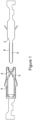
Figure 1 is a cross sectional view of a male and female electrical terminal, each terminal comprising a substrate and a metallic conductive layer provided on the substrate according to a specific implementation; and -
Figure 2 is a flow diagram illustrating a process for manufacturing an electrical terminal according to a specific implementation of the present invention. - In
Figure 1 there is shown a maleelectrical terminal 2 and a femaleelectrical terminal 4 according to the invention. Eachterminal substrate 6. In the embodiment shown, thesubstrate 6 is formed from copper alloy, but alternative metals may be used such as aluminium alloy. Eachterminal conductive layer 8 provided on thesubstrate 6. - Referring now to
Figure 2 , the metallicconductive layer 8 has anintermetallic phase 10 of silver and indium. In other embodiments not shown, the intermetallic phase may be formed of silver and any other suitable chemical. Other suitable chemicals include the post-transition metals gallium or tin. The presence of indium protects the silver in theconductive layer 8 from environmental effects, wear and tarnishing. Further, as indium is softer than silver, the necessary insertion force for theterminals - In the illustrated embodiment, the predominant wt% intermetallic compound in the intermetallic phase is AgIn2. The predominant compound can be controlled depending on the conditions of formation of the intermetallic phase. Other compounds may also be present, such as Ag2In. In other embodiments, where bismuth or gallium is present, the predominant compound may be Ag3Ga2 respectively. Again, other compounds of silver-bismuth or silver-gallium may be present.
- The concentration of indium in the
intermetallic phase 10 increases in a direction heading away from thesubstrate 6. In other words, the concentration of indium is lowest at a location close to thesubstrate 6 and highest at a location furthest away from thesubstrate 6. Further, in contrast, the concentration of silver in the intermetallic phase decreases in a direction heading away from thesubstrate 6. The concentration of silver therefore is greatest at a location close to thesubstrate 6 and lowest at a location furthest away from the substrate. In other embodiments where gallium or tin may be used in place of indium, or alongside indium, the concentration of these elements will again be lowest close to the substrate and highest further from the substrate. - The
terminals barrier layer 12 located between thesubstrate 6 and theintermetallic phase 10. Thebarrier layer 12 prevents diffusion of the silver into the substrate. In the illustrated embodiment, thebarrier layer 12 is formed from nickel, but alternative materials may be used such as copper, aluminium, or alloys thereof. The thickness of thebarrier layer 12 is preferably between 1 and 2 µm, but may alternatively be between 0.5 and 3 µm or 0.1 and 10 µm. - In the embodiment shown, the
terminals silver layer 14. In another embodiment, not shown, the metallicconductive layer 8 comprises a bismuth layer arranged on the silver layer. Thesilver layer 14 is located between thesubstrate 6 andintermetallic phase 10, or between the substrate and the bismuth layer. More specifically, thesilver layer 14 is located between thebarrier layer 12 and theintermetallic phase 10 or bismuth layer. - In the embodiment shown, the
terminals indium layer 16. The indium layer is the outermost layer of the metallicconductive layer 8. Thus, theintermetallic phase 10 is located between theindium layer 16 andsilver layer 14,barrier layer 12 andsubstrate 6. The indium layer has a thickness of up to 5 µm. In other embodiments, the outermost layer may be a gallium, bismuth or tin layer, or combinations thereof, possibly also with indium. - The
indium layer 16, which may also be formed from any of gallium, bismuth or tin or combination thereof, has atop surface 16a, andbottom surface 16b wherein thetop surface 16a is at one side of the layer and thebottom surface 16b is at an opposing side. Theintermetallic phase 10 further has atop surface 10a and abottom surface 10b wherein thetop surface 10a is at one side of the layer and thebottom surface 10b is at an opposing side. Thebottom surface 16b of theindium layer 16 is in contact with thetop surface 10a of theintermetallic phase 10. Thetop surface 16a of the indium layer is ideally exposed and represents the outermost surface of theconductive layer 8. Thesilver layer 14 further has atop surface 14a and abottom surface 14b wherein thetop surface 14a is at one side of the layer and thebottom surface 14b is at an opposing side. Thebottom surface 10b of the intermetallic phase is in contact with thetop surface 14a of the silver layer. Thebarrier layer 12 further has atop surface 12a and abottom surface 12b wherein thetop surface 12a is at one side of the layer and thebottom surface 12b is at an opposing side. Thebottom surface 14b of the silver layer is in contact with thetop surface 12a of the barrier layer. Thesubstrate 6 has atop layer 6a. Thetop layer 6a of thesubstrate 6 is in contact with thebottom surface 12b of the barrier layer. - In use, the male
electrical terminal 2 is inserted into the femaleelectrical terminal 4. The metallicconductive layers 8 of each of the male and femaleelectrical terminals terminals Such terminals terminals - The terminals of the present invention can be formed by reel-to-reel plating. In reel-to-reel plating, strips of material or plated and then formed into the desired product. There are four known reel-to-reel plating techniques typically used to deposit metals on terminals: immersion plating, strip technique, brush plating, and spot technique. Immersion plating is typically used for depositing large quantities of metals, whereas spot technique offers higher selectivity to save metal quantity.
- In reel-to-reel plating, rolled blank material or pre-stamped material is de-reeled and will be fed through multiple process including rinsing, plating and drying, before being rewound onto a new real after having been plated.
- The terminals of the present invention can be formed by an electro-plating process. In electro-plating, the substrate is placed into an electrolyte solution in an electrolysis bath. An anode is present in the electrolyte solution which comprises the desired coating material. The substrate is the cathode. The transfer of the material from the cathode is achieved by setting the electrolysis parameters such as bath temperature, pH, voltage, current, electrolyte concentration and rinsing steps. The skilled person will understand that many combinations of parameters exist that will achieve the adequate plating thickness and metal quality.
- The
terminals substrate 6 is provided. Next, thebarrier layer 12 is formed by depositing nickel on thesubstrate 6 to a thickness of 1-2 µm. Alternatively, the nickel may be deposited to a thickness of 0.5-3 µm or 0.1-10 µm. Further alternatively, the barrier layer may be formed by depositing any one of or a combination of the group comprising: nickel, copper, aluminium or alloys thereof. - Next,
silver 14 is deposited indirectly on thesubstrate 6 to form a silver layer. By "indirectly" we mean the silver is deposited on thebarrier layer 12 which in turn is deposited on thesubstrate 6. In other embodiments where no barrier layer is present, thesilver 14 may be deposited directly on thesubstrate 6. Thesilver 14 is deposited to a thickness of between 4 and 5 µm. Alternatively, thesilver 14 may be deposited to a thickness of between 0.5 and 10 µm or 2 and 6 µm. - Next,
indium 16 is deposited on thesilver layer 14 to form anindium layer 16. Theindium 16 is deposited to a thickness of between 0.5 and 1 µm but may be deposited to thicknesses of between 0.1 and 5 µm, 0.3 and 2 µm. Alternatively, gallium, bismuth or tin may be deposited rather than indium, or combinations of any of indium, gallium, bismuth or tin. - Before processing to form the intermetallic phase, the
bottom surface 16b of theindium layer 16 is in contact with thetop surface 14a of the silver layer; thebottom surface 14b of the silver layer is in contact with thetop surface 12a of the barrier layer, and; thetop layer 6a of thesubstrate 6 is in contact with thebottom surface 12b of the barrier layer. - After the metals have been deposited and the layers formed, the
terminals intermetallic phase 10. Theintermetallic phase 10 is formed by preferably tempering 16 and then storing 18 theterminals intermetallic phase 10 may be also be formed by either a temperingstep 16 orstorage step 18 alone. During tempering or storing, the thickness of theintermetallic phase 10 increases, and consequently the thickness of thesilver layer 14 andindium layer 16 decreases. After tempering or storing, the thickness of the indium, gallium or tin layers should be at least 50% of the initial thickness (i.e., the thickness before tempering). For example, the indium may deposited to a thickness of between 0.3 and 2 µm. After tempering or storage, the indium layer should have a thickness of between 0.15 and 2 µm. - The tempering
step 16 involves heating theterminal terminal - In the
storage step 18, theterminal intermetallic phase 10 to form. Ideally, theterminal - Unless defined otherwise, all technical and scientific terms used herein have the same meaning as commonly understood to one of ordinary skill in the art to which the presently described subject matter pertains.
- Where a range of values is provided, for example, concentration ranges, percentage ranges, or ratio ranges, it is understood that each intervening value, to the tenth of the unit of the lower limit, unless the context clearly dictates otherwise, between the upper and lower limit of that range and any other stated or intervening value in that stated range, is encompassed within the described subject matter. The upper and lower limits of these smaller ranges may independently be included in the smaller ranges, and such embodiments are also encompassed within the described subject matter, subject to any specifically excluded limit in the stated range. Where the stated range includes one or both of the limits, ranges excluding either or both of those included limits are also included in the described subject matter.
- It should be understood that the terms "a" and "an" as used above and elsewhere herein refer to "one or more" of the enumerated components. It will be clear to one of ordinary skill in the art that the use of the singular includes the plural unless specifically stated otherwise. Therefore, the terms "a," "an" and "at least one" are used interchangeably in this application.
- Unless otherwise indicated, all numbers expressing quantities of ingredients, properties such as size, weight, reaction conditions and so forth used in the specification and claims are to the understood as being modified in all instances by the term "about". Accordingly, unless indicated to the contrary, the numerical parameters set forth in the following specification and attached claims are approximations that may vary depending upon the desired properties sought to be obtained by the present subject matter. At the very least, and not as an attempt to limit the application of the doctrine of equivalents to the scope of the claims, each numerical parameter should at least be construed in light of the number of reported significant digits and by applying ordinary rounding techniques.
- Throughout the application, descriptions of various embodiments use "comprising" language; however, it will be understood by one of skill in the art, that in some instances, an embodiment can alternatively be described using the language "consisting essentially of or "consisting of."
Claims (15)
- An electrical terminal comprising a substrate and a metallic conductive layer provided on the substrate characterised in that the metallic conductive layer comprises either:a silver layer and an intermetallic phase of silver and one or a combination of indium or gallium, or;a silver layer and a bismuth layer, wherein the silver layer is located between the substrate and the bismuth layer.
- The terminal as claimed in claim 1, wherein the intermetallic phase optionally comprises tin, and wherein the concentration of indium, gallium or tin in the intermetallic phase increases in a direction extending away from the substrate.
- The terminal as claimed in claim 1 or claim 2, wherein:• the intermetallic phase comprises indium and a wt% predominant intermetallic compound in the intermetallic phase is AgIn2;• the intermetallic phase comprises gallium and a wt% predominant intermetallic compound in the intermetallic phase is Ag3Ga2; and/or Ag2Ga; or• the intermetallic phase comprises tin and a wt% predominant intermetallic compound in the intermetallic phase is Ag3Sn;
- The terminal as claimed in any preceding claim further comprising: a barrier layer between the substrate and the silver layer, optionally wherein the barrier layer comprises nickel.
- The terminal as claimed in any preceding claim further comprising a layer of any one or a combination of the group comprising: indium, gallium, bismuth or tin.
- The terminal as claimed in claim 5 wherein the layer of any one or a combination of the group comprising: indium, gallium, bismuth or tin is disposed directly on the intermetallic phase, and wherein the intermetallic phase is disposed directly on the silver layer, and optionally wherein the silver layer is disposed directly on the barrier layer, and optionally wherein the barrier layer is disposed directly on the substrate.
- A process for manufacturing the terminal of claim 1, the process comprising the steps of:depositing silver directly or indirectly on a substrate to form a silver layer;depositing any one or a combination of the group comprising: indium, gallium, bismuth or tin on the silver layer, to form a layer of any one or a combination of the group comprising: indium, gallium, bismuth or tin.
- The process of claim 8 comprising the step of tempering and/or storing the terminal to form an intermetallic phase comprising silver and any one or a combination of the group comprising: indium, gallium or tin.
- The process of claim 7 or claim 8 wherein the silver is deposited to a thickness of between 0.5 and 10 µm.
- The process of any one of claims 7 to 9 wherein the indium, gallium, bismuth or tin or combination thereof is deposited to a thickness of between 0.1 and 5 µm.
- The process of any one of claims 7 to 10 wherein the terminal is tempered by heating to a temperature within a range 50°C below the melting point of the indium, gallium, bismuth or tin.
- The process of claim 11 wherein the terminal is tempered by heating for between 5 seconds and 5 minutes.
- The process of any one of claims 7 to 12 wherein the terminal is stored for between 2 hours and 7 days after the indium, gallium, bismuth, tin or combination thereof is deposited.
- The process of any one of claims 7 to 13 comprising initially forming a barrier layer on the substrate before depositing the silver and thereafter depositing the silver on the barrier layer.
- The process of claim 14 wherein the barrier layer is formed by depositing any one of or a combination of the group comprising: nickel, copper, aluminium or alloys thereof, and optionally wherein the barrier layer is deposited to a thickness of between 0.1 and 10 µm.
Priority Applications (1)
| Application Number | Priority Date | Filing Date | Title |
|---|---|---|---|
| EP22213244.1A EP4386113A1 (en) | 2022-12-13 | 2022-12-13 | Electrical terminal with metal conductive layer comprising silver |
Applications Claiming Priority (1)
| Application Number | Priority Date | Filing Date | Title |
|---|---|---|---|
| EP22213244.1A EP4386113A1 (en) | 2022-12-13 | 2022-12-13 | Electrical terminal with metal conductive layer comprising silver |
Publications (1)
| Publication Number | Publication Date |
|---|---|
| EP4386113A1 true EP4386113A1 (en) | 2024-06-19 |
Family
ID=84602171
Family Applications (1)
| Application Number | Title | Priority Date | Filing Date |
|---|---|---|---|
| EP22213244.1A Pending EP4386113A1 (en) | 2022-12-13 | 2022-12-13 | Electrical terminal with metal conductive layer comprising silver |
Country Status (1)
| Country | Link |
|---|---|
| EP (1) | EP4386113A1 (en) |
Citations (6)
| Publication number | Priority date | Publication date | Assignee | Title |
|---|---|---|---|---|
| JP2004238689A (en) * | 2003-02-06 | 2004-08-26 | Kyowa Densen Kk | Plating materials, terminals for electronic components, connectors, lead members, and semiconductor devices |
| US20130224515A1 (en) * | 2012-02-29 | 2013-08-29 | Rohm And Haas Electronic Materials Llc | Method of preventing silver tarnishing |
| US9576693B2 (en) * | 2011-09-20 | 2017-02-21 | Jx Nippon Mining & Metals Corporation | Metal material for electronic component and method for manufacturing the same |
| US20190234994A1 (en) * | 2018-02-01 | 2019-08-01 | Jx Nippon Mining & Metals Corporation | Surface Treated Metal Material For Burn-In Test Socket, Connector For Burn-In Test Socket And Burn-In Test Socket Using The Same |
| US10530084B2 (en) * | 2012-06-27 | 2020-01-07 | Jx Nippon Mining & Metals Corporation | Metallic material for electronic components and method for producing same, and connector terminals, connectors and electronic components using same |
| US20210158990A1 (en) * | 2017-08-08 | 2021-05-27 | Mitsubishi Materials Corporation | Terminal material with silver coating film and terminal with silver coating film |
-
2022
- 2022-12-13 EP EP22213244.1A patent/EP4386113A1/en active Pending
Patent Citations (6)
| Publication number | Priority date | Publication date | Assignee | Title |
|---|---|---|---|---|
| JP2004238689A (en) * | 2003-02-06 | 2004-08-26 | Kyowa Densen Kk | Plating materials, terminals for electronic components, connectors, lead members, and semiconductor devices |
| US9576693B2 (en) * | 2011-09-20 | 2017-02-21 | Jx Nippon Mining & Metals Corporation | Metal material for electronic component and method for manufacturing the same |
| US20130224515A1 (en) * | 2012-02-29 | 2013-08-29 | Rohm And Haas Electronic Materials Llc | Method of preventing silver tarnishing |
| US10530084B2 (en) * | 2012-06-27 | 2020-01-07 | Jx Nippon Mining & Metals Corporation | Metallic material for electronic components and method for producing same, and connector terminals, connectors and electronic components using same |
| US20210158990A1 (en) * | 2017-08-08 | 2021-05-27 | Mitsubishi Materials Corporation | Terminal material with silver coating film and terminal with silver coating film |
| US20190234994A1 (en) * | 2018-02-01 | 2019-08-01 | Jx Nippon Mining & Metals Corporation | Surface Treated Metal Material For Burn-In Test Socket, Connector For Burn-In Test Socket And Burn-In Test Socket Using The Same |
Similar Documents
| Publication | Publication Date | Title |
|---|---|---|
| US5098485A (en) | Method of making electrically insulating metallic oxides electrically conductive | |
| US10640880B2 (en) | Plated material and connecting terminal using same | |
| CN101318390B (en) | Remelting plating Sn material and electronic component using the same | |
| US6495001B2 (en) | Method for manufacturing a metallic composite strip | |
| CN1455829A (en) | Metal-plated material and method for preparation, and electric and electronic parts using same | |
| CN101051535B (en) | Conductor for wiring, manufacturing method thereof, terminal connection portion, lead-free solder alloy | |
| CN105358741A (en) | Method for producing plated laminate, and plated laminate | |
| CN102522646A (en) | Wiring conductor, method for fabricating same, terminal connecting assembly, and Pb-free solder alloy | |
| JP2006183068A (en) | Conductive material for connecting part and method for manufacturing the conductive material | |
| JPH08176883A (en) | Method for producing Sn alloy plated material | |
| EP3751667A1 (en) | Electrical terminal | |
| CN110997985A (en) | Silver-coated membrane terminal material and silver-coated membrane terminal | |
| JP7302364B2 (en) | Connector terminal materials and connector terminals | |
| JPH04329891A (en) | Tin plated copper alloy material and its production | |
| JP5635794B2 (en) | Conductive member and manufacturing method thereof | |
| JPH0855521A (en) | Current-carrying member and manufacturing method thereof | |
| CN100379092C (en) | Terminal with surface layer formed, part and product including the terminal, and method for manufacturing the terminal | |
| Lindborg et al. | Intermetallic growth and contact resistance of tin contacts after aging | |
| WO2019087926A1 (en) | Anticorrosive terminal material, anticorrosive terminal, and electric wire end structure | |
| EP4142063A1 (en) | Electric contact having a multilayered coating structure | |
| JPH0217637B2 (en) | ||
| WO2022168740A1 (en) | Anti-corrosion terminal material for aluminum core wires, anti-corrosion terminal, and electric wire end part structure | |
| JP7230570B2 (en) | Conductive member for connector terminal and connector terminal | |
| WO1999006612A1 (en) | Two layer solderable tin coating | |
| JP7087732B2 (en) | Conductive member for connector terminal and connector terminal |
Legal Events
| Date | Code | Title | Description |
|---|---|---|---|
| PUAI | Public reference made under article 153(3) epc to a published international application that has entered the european phase |
Free format text: ORIGINAL CODE: 0009012 |
|
| STAA | Information on the status of an ep patent application or granted ep patent |
Free format text: STATUS: THE APPLICATION HAS BEEN PUBLISHED |
|
| AK | Designated contracting states |
Kind code of ref document: A1 Designated state(s): AL AT BE BG CH CY CZ DE DK EE ES FI FR GB GR HR HU IE IS IT LI LT LU LV MC ME MK MT NL NO PL PT RO RS SE SI SK SM TR |
|
| RAP1 | Party data changed (applicant data changed or rights of an application transferred) |
Owner name: APTIV TECHNOLOGIES AG |
|
| RAP3 | Party data changed (applicant data changed or rights of an application transferred) |
Owner name: APTIV TECHNOLOGIES AG |
|
| STAA | Information on the status of an ep patent application or granted ep patent |
Free format text: STATUS: REQUEST FOR EXAMINATION WAS MADE |
|
| 17P | Request for examination filed |
Effective date: 20241212 |