EP4382998A1 - Display device and method for driving peep-proof state switching film thereof - Google Patents
Display device and method for driving peep-proof state switching film thereof Download PDFInfo
- Publication number
- EP4382998A1 EP4382998A1 EP21816306.1A EP21816306A EP4382998A1 EP 4382998 A1 EP4382998 A1 EP 4382998A1 EP 21816306 A EP21816306 A EP 21816306A EP 4382998 A1 EP4382998 A1 EP 4382998A1
- Authority
- EP
- European Patent Office
- Prior art keywords
- peep
- electrodes
- display device
- substrate
- liquid crystal
- Prior art date
- Legal status (The legal status is an assumption and is not a legal conclusion. Google has not performed a legal analysis and makes no representation as to the accuracy of the status listed.)
- Pending
Links
Images



Classifications
-
- G—PHYSICS
- G02—OPTICS
- G02F—OPTICAL DEVICES OR ARRANGEMENTS FOR THE CONTROL OF LIGHT BY MODIFICATION OF THE OPTICAL PROPERTIES OF THE MEDIA OF THE ELEMENTS INVOLVED THEREIN; NON-LINEAR OPTICS; FREQUENCY-CHANGING OF LIGHT; OPTICAL LOGIC ELEMENTS; OPTICAL ANALOGUE/DIGITAL CONVERTERS
- G02F1/00—Devices or arrangements for the control of the intensity, colour, phase, polarisation or direction of light arriving from an independent light source, e.g. switching, gating or modulating; Non-linear optics
- G02F1/01—Devices or arrangements for the control of the intensity, colour, phase, polarisation or direction of light arriving from an independent light source, e.g. switching, gating or modulating; Non-linear optics for the control of the intensity, phase, polarisation or colour
- G02F1/13—Devices or arrangements for the control of the intensity, colour, phase, polarisation or direction of light arriving from an independent light source, e.g. switching, gating or modulating; Non-linear optics for the control of the intensity, phase, polarisation or colour based on liquid crystals, e.g. single liquid crystal display cells
- G02F1/1323—Arrangements for providing a switchable viewing angle
-
- G—PHYSICS
- G02—OPTICS
- G02F—OPTICAL DEVICES OR ARRANGEMENTS FOR THE CONTROL OF LIGHT BY MODIFICATION OF THE OPTICAL PROPERTIES OF THE MEDIA OF THE ELEMENTS INVOLVED THEREIN; NON-LINEAR OPTICS; FREQUENCY-CHANGING OF LIGHT; OPTICAL LOGIC ELEMENTS; OPTICAL ANALOGUE/DIGITAL CONVERTERS
- G02F1/00—Devices or arrangements for the control of the intensity, colour, phase, polarisation or direction of light arriving from an independent light source, e.g. switching, gating or modulating; Non-linear optics
- G02F1/01—Devices or arrangements for the control of the intensity, colour, phase, polarisation or direction of light arriving from an independent light source, e.g. switching, gating or modulating; Non-linear optics for the control of the intensity, phase, polarisation or colour
- G02F1/13—Devices or arrangements for the control of the intensity, colour, phase, polarisation or direction of light arriving from an independent light source, e.g. switching, gating or modulating; Non-linear optics for the control of the intensity, phase, polarisation or colour based on liquid crystals, e.g. single liquid crystal display cells
- G02F1/133—Constructional arrangements; Operation of liquid crystal cells; Circuit arrangements
- G02F1/13306—Circuit arrangements or driving methods for the control of single liquid crystal cells
-
- G—PHYSICS
- G02—OPTICS
- G02F—OPTICAL DEVICES OR ARRANGEMENTS FOR THE CONTROL OF LIGHT BY MODIFICATION OF THE OPTICAL PROPERTIES OF THE MEDIA OF THE ELEMENTS INVOLVED THEREIN; NON-LINEAR OPTICS; FREQUENCY-CHANGING OF LIGHT; OPTICAL LOGIC ELEMENTS; OPTICAL ANALOGUE/DIGITAL CONVERTERS
- G02F1/00—Devices or arrangements for the control of the intensity, colour, phase, polarisation or direction of light arriving from an independent light source, e.g. switching, gating or modulating; Non-linear optics
- G02F1/01—Devices or arrangements for the control of the intensity, colour, phase, polarisation or direction of light arriving from an independent light source, e.g. switching, gating or modulating; Non-linear optics for the control of the intensity, phase, polarisation or colour
- G02F1/13—Devices or arrangements for the control of the intensity, colour, phase, polarisation or direction of light arriving from an independent light source, e.g. switching, gating or modulating; Non-linear optics for the control of the intensity, phase, polarisation or colour based on liquid crystals, e.g. single liquid crystal display cells
- G02F1/133—Constructional arrangements; Operation of liquid crystal cells; Circuit arrangements
- G02F1/1333—Constructional arrangements; Manufacturing methods
- G02F1/1343—Electrodes
- G02F1/134309—Electrodes characterised by their geometrical arrangement
-
- G—PHYSICS
- G02—OPTICS
- G02F—OPTICAL DEVICES OR ARRANGEMENTS FOR THE CONTROL OF LIGHT BY MODIFICATION OF THE OPTICAL PROPERTIES OF THE MEDIA OF THE ELEMENTS INVOLVED THEREIN; NON-LINEAR OPTICS; FREQUENCY-CHANGING OF LIGHT; OPTICAL LOGIC ELEMENTS; OPTICAL ANALOGUE/DIGITAL CONVERTERS
- G02F1/00—Devices or arrangements for the control of the intensity, colour, phase, polarisation or direction of light arriving from an independent light source, e.g. switching, gating or modulating; Non-linear optics
- G02F1/01—Devices or arrangements for the control of the intensity, colour, phase, polarisation or direction of light arriving from an independent light source, e.g. switching, gating or modulating; Non-linear optics for the control of the intensity, phase, polarisation or colour
- G02F1/13—Devices or arrangements for the control of the intensity, colour, phase, polarisation or direction of light arriving from an independent light source, e.g. switching, gating or modulating; Non-linear optics for the control of the intensity, phase, polarisation or colour based on liquid crystals, e.g. single liquid crystal display cells
- G02F1/133—Constructional arrangements; Operation of liquid crystal cells; Circuit arrangements
- G02F1/1333—Constructional arrangements; Manufacturing methods
- G02F1/1347—Arrangement of liquid crystal layers or cells in which the final condition of one light beam is achieved by the addition of the effects of two or more layers or cells
-
- G—PHYSICS
- G02—OPTICS
- G02F—OPTICAL DEVICES OR ARRANGEMENTS FOR THE CONTROL OF LIGHT BY MODIFICATION OF THE OPTICAL PROPERTIES OF THE MEDIA OF THE ELEMENTS INVOLVED THEREIN; NON-LINEAR OPTICS; FREQUENCY-CHANGING OF LIGHT; OPTICAL LOGIC ELEMENTS; OPTICAL ANALOGUE/DIGITAL CONVERTERS
- G02F1/00—Devices or arrangements for the control of the intensity, colour, phase, polarisation or direction of light arriving from an independent light source, e.g. switching, gating or modulating; Non-linear optics
- G02F1/01—Devices or arrangements for the control of the intensity, colour, phase, polarisation or direction of light arriving from an independent light source, e.g. switching, gating or modulating; Non-linear optics for the control of the intensity, phase, polarisation or colour
- G02F1/13—Devices or arrangements for the control of the intensity, colour, phase, polarisation or direction of light arriving from an independent light source, e.g. switching, gating or modulating; Non-linear optics for the control of the intensity, phase, polarisation or colour based on liquid crystals, e.g. single liquid crystal display cells
- G02F1/133—Constructional arrangements; Operation of liquid crystal cells; Circuit arrangements
- G02F1/1333—Constructional arrangements; Manufacturing methods
- G02F1/1347—Arrangement of liquid crystal layers or cells in which the final condition of one light beam is achieved by the addition of the effects of two or more layers or cells
- G02F1/13471—Arrangement of liquid crystal layers or cells in which the final condition of one light beam is achieved by the addition of the effects of two or more layers or cells in which all the liquid crystal cells or layers remain transparent, e.g. FLC, ECB, DAP, HAN, TN, STN, SBE-LC cells
-
- G—PHYSICS
- G02—OPTICS
- G02F—OPTICAL DEVICES OR ARRANGEMENTS FOR THE CONTROL OF LIGHT BY MODIFICATION OF THE OPTICAL PROPERTIES OF THE MEDIA OF THE ELEMENTS INVOLVED THEREIN; NON-LINEAR OPTICS; FREQUENCY-CHANGING OF LIGHT; OPTICAL LOGIC ELEMENTS; OPTICAL ANALOGUE/DIGITAL CONVERTERS
- G02F1/00—Devices or arrangements for the control of the intensity, colour, phase, polarisation or direction of light arriving from an independent light source, e.g. switching, gating or modulating; Non-linear optics
- G02F1/01—Devices or arrangements for the control of the intensity, colour, phase, polarisation or direction of light arriving from an independent light source, e.g. switching, gating or modulating; Non-linear optics for the control of the intensity, phase, polarisation or colour
- G02F1/13—Devices or arrangements for the control of the intensity, colour, phase, polarisation or direction of light arriving from an independent light source, e.g. switching, gating or modulating; Non-linear optics for the control of the intensity, phase, polarisation or colour based on liquid crystals, e.g. single liquid crystal display cells
- G02F1/133—Constructional arrangements; Operation of liquid crystal cells; Circuit arrangements
- G02F1/136—Liquid crystal cells structurally associated with a semi-conducting layer or substrate, e.g. cells forming part of an integrated circuit
- G02F1/1362—Active matrix addressed cells
- G02F1/136286—Wiring, e.g. gate line, drain line
-
- G—PHYSICS
- G02—OPTICS
- G02F—OPTICAL DEVICES OR ARRANGEMENTS FOR THE CONTROL OF LIGHT BY MODIFICATION OF THE OPTICAL PROPERTIES OF THE MEDIA OF THE ELEMENTS INVOLVED THEREIN; NON-LINEAR OPTICS; FREQUENCY-CHANGING OF LIGHT; OPTICAL LOGIC ELEMENTS; OPTICAL ANALOGUE/DIGITAL CONVERTERS
- G02F1/00—Devices or arrangements for the control of the intensity, colour, phase, polarisation or direction of light arriving from an independent light source, e.g. switching, gating or modulating; Non-linear optics
- G02F1/01—Devices or arrangements for the control of the intensity, colour, phase, polarisation or direction of light arriving from an independent light source, e.g. switching, gating or modulating; Non-linear optics for the control of the intensity, phase, polarisation or colour
- G02F1/13—Devices or arrangements for the control of the intensity, colour, phase, polarisation or direction of light arriving from an independent light source, e.g. switching, gating or modulating; Non-linear optics for the control of the intensity, phase, polarisation or colour based on liquid crystals, e.g. single liquid crystal display cells
- G02F1/133—Constructional arrangements; Operation of liquid crystal cells; Circuit arrangements
- G02F1/136—Liquid crystal cells structurally associated with a semi-conducting layer or substrate, e.g. cells forming part of an integrated circuit
- G02F1/1362—Active matrix addressed cells
- G02F1/1368—Active matrix addressed cells in which the switching element is a three-electrode device
Definitions
- the present application relates to a field of display technologies, especially to a display device with an anti-peep function and an anti-peep state switching film driving method thereof.
- an anti-peep display is visible within a certain small viewing angle, and displayed imaged cannot be viewed in a large viewing angle, which performs an anti-peep effect.
- ACF advance light control film
- Conventional anti-peep displays bring users excellent privacy.
- the anti-peep displays are intensively used in personal information display devices in public places but an anti-peep function cannot be switched to a sharing state, which makes use scenarios and use functions limited and a market value thereof is difficult the exert.
- display devices used for meeting rooms can switch to an anti-peep state according to use scenarios.
- the display device can switch on the anti-peep state to reduce a viewing angle.
- a larger display viewing angle is required to meet the needs of viewers in different locations to clearly view the display contents.
- the conventional anti-peep display device function are relatively simple functions and cannot switch the anti-peep state. It is required to provide a display device that can switch a display effect of a anti-peep state or a sharing state according to use scenarios to fill a market gap.
- the present application embodiment provides a display device and an anti-peep state switching film driving method thereof to solve a technical issue that a conventional anti-peep display device only has an anti-peep state and cannot select the anti-peep state or a sharing state according to application scenarios.
- the present invention provides a display device capable of switching an anti-peep state, comprising:
- the anti-peep state switching film comprises a middle region and anti-peep regions located on a central region along a horizontal display direction, a vertical display direction, and a diagonal display direction, and an area of the anti-peep regions is greater than an area of the central region.
- the driver electrodes are distributed on the central region and the anti-peep regions located on a periphery of the central region, a difference of driving voltages of each of the driver electrodes corresponding to the central region and the anti-peep regions respectively is different from that of another of the driver electrodes, and rotational angles of the liquid crystals in the central region and the anti-peep regions respectively are different.
- the difference of the driving voltages located in the central region is the same as the difference of the driving voltages located in the anti-peep regions on the periphery of the central region; when the liquid crystal display panel is in the sharing state, the driver electrodes in regions corresponding to the different electrodes drive the liquid crystals to rotate by different differences of the driving voltages, and the rotational angle of the liquid crystals of the anti-peep regions is greater than the rotational angle of the liquid crystals of the central region.
- the driver electrodes comprise a common electrode located on the first substrate or the second substrate, and release electrodes relatively located on the other of the first substrate and the second substrate, wherein the common electrode is disposed as an entire surface, the release electrodes are arranged in an array, and adjacent ones of the release electrodes are insulative to each other to individually receive a time signal, the common electrode and the release electrodes are electrified to constitute a vertical electrical field.
- the release electrodes comprise strip electrodes arranged in an array along a horizontal display direction of the liquid crystal display panel, adjacent ones of the strip electrodes are disposed at an interval, and the strip electrodes are correspondingly distributed on a middle display region and a display region relatively located on two sides of the middle display region.
- the release electrodes is annularly and radially disposed, the release electrodes comprise a central electrode pattern, and annular electrode patterns extending outward from the central electrode pattern, the central electrode pattern is correspondingly located in a central display region of the liquid crystal display panel, and the annular electrode patterns correspondingly covers the display region outside the central display region.
- the central electrode and the annular electrodes are hollow and circular electrodes, and inner diameters of the annular electrodes gradually increase from a center of the anti-peep state switching film to an edge, and shapes of the annular electrodes extending outward gradually fit an edge outline of the anti-peep state switching film.
- a driver integrated circuit IC
- a time control circuit connected to the driver IC
- a driving line connected to the time control circuit
- the driving line comprises a gate electrode line disposed along a first direction and a data line disposed along second direction
- the release electrodes are electrically connected the gate electrode line and the data line through thin film transistors.
- the display device further comprises a scan line, a data line insulatively intersecting the scan line, and a thin film transistor connected to the scan line and the data line, a gate electrode of the thin film transistor is connected to the scan line, a source electrode is connected to the data line, a drain electrode is connected to release electrodes, the release electrodes and the common electrode form a difference of voltages constitute a liquid crystal capacitor and a storage capacitor.
- the anti-peep state switching film comprises a middle region and anti-peep regions located on two sides of the middle region, and a distribution sequence of the anti-peep region, the middle region, and the anti-peep region is along a horizontal display direction of the liquid crystal display panel; and an area of the anti-peep regions is greater than an area of the middle region, and areas of the anti-peep regions on the two sides of the middle region are the same.
- the driver electrodes comprise a common electrode located on the first substrate or the second substrate and release electrodes located on the same one of the first substrate and the second substrate with the common electrode, wherein the common electrode is disposed in a comb shape, the release electrodes are disposed insulatively to one another and arranged in an array to individually receive a time signal, the release electrodes are correspondingly disposed in gaps of the common electrode, and the common electrode and the release electrodes are electrified to constitute a horizontal electrical field.
- the release electrodes comprise strip electrodes arranged in an array along the horizontal display direction of the liquid crystal display panel
- the common electrode comprises a comb electrode and a common line connected to the comb electrode
- the strip electrodes are embedded in a tooth electrode formed by the comb electrode and the common line.
- a driving voltage of the strip electrodes corresponding to the middle region and a driving voltage of the corresponding to the anti-peep regions are different, the comb electrode receives a constant voltage, and the comb electrode and adjacent one of the strip electrodes form a horizontal electrical field to drive the liquid crystals to rotate.
- a backlight module is further disposed on the light incident side of the liquid crystal display panel, and the backlight module comprises:
- the anti-peep film is a microscopic shutter, and an interval of the microscopic shutter is 0.07mm.
- the liquid crystal layer is one of vertically rotational type liquid crystals, twisted nematic type liquid crystals, or horizontally rotational type liquid crystals.
- an anti-peep state switching film comprises: a first substrate and a second substrate disposed oppositely, a liquid crystal layer located between the first substrate and the second substrate, and driver electrodes located on at least one side of the liquid crystal layer, the driver electrodes comprise a common electrode and release electrodes disposed opposite to the common electrode, the release electrodes are distributed insulatively, and an electrical field is generated between the electrified release electrodes and the common electrode to drive the liquid crystals to rotate; wherein the driving method comprises:
- the method further comprises:
- the liquid crystals of the anti-peep state switching film are at a pre-tilt rotational angle, and the liquid crystals in a region corresponding to each of the release electrodes are at the same rotational angle to reduce a light exiting range.
- the present invention provides a display device and an anti-peep state switching film driving method thereof.
- the display device has an anti-peep display function, and an anti-peep state switching film is also disposed on the display device.
- Selectively electrifying the anti-peep state switching film can change a display viewing angle of the display device.
- a time control cooperatively supplies each of the release electrodes with a driving signal individually to achieve switching between an anti-peep state and a sharing state at will such that application scenarios of the anti-peep display becomes more extensive.
- the present application provides a display device with an anti-peep function and an anti-peep state switching film driving method thereof.
- the present application embodiment provides a display device including an anti-peep function, and detailed descriptions in conjunction with FIGs. 1 to 4 are as follows.
- FIG. 1 illustrates the display device provided by the present invention comprising a liquid crystal display panel 101, a backlight module and an anti-peep film 102 located on a light incident side of the liquid crystal display panel 101, and an anti-peep state switching film 103 located on a light exiting side of the liquid crystal display panel 101.
- the backlight module comprises a light guide plate 104, a light source located on a light incident side of the light guide plate 104, a diffuser plate 105 located on a light exiting side of the light guide plate 104, and a prism film 106 located on a light exiting side of the diffuser plate 105.
- the anti-peep film 102 is located on a light exiting side of the prism film 106.
- the anti-peep film 102 is disposed between the backlight module and the liquid crystal display panel 101 and is configured to filter partial backlight entering the liquid crystal display panel 101 into a light in an specific angle.
- the anti-peep film 102 exists in form of a microscopic shutter.
- An interval of the microscopic shutter is 0.07mm, and a fence of the microscopic shutter has a certain height and can absorb and limit passing light in the viewing angle.
- a right viewing angle serves as a normal, a viewing angle of light of the anti-peep film 102 can be 60 ⁇ 4 degrees.
- the anti-peep state switching film 103 is disposed on the light exiting side of the liquid crystal display panel 101.
- the anti-peep state switching film 103 also serves as a light filtering layer and can adjust an angle of exiting light of the liquid crystal display panel 101, which not only achieves a sharing state of a large viewing angle, but also achieves a anti-peep state of a small viewing angle.
- FIGs 2a and 2b are schematic structural views of the anti-peep state switching film, and the anti-peep state switching film comprises a first substrate 201, a second substrate 202 disposed opposite to the first substrate 201, a liquid crystal layer 203 located between the first substrate 201 and the second substrate 202, and driver electrodes located on at least one side of the liquid crystal layer 203.
- a driving principle of the liquid crystal layer 203 of the anti-peep state switching film is similar to a driving principle of the liquid crystal display panel, both are generating a vertical electrical field or a horizontal electrical field through the driver electrodes to drive the liquid crystals to rotate to adjust light of transmission light to further adjust a viewing angle of the liquid crystal display panel.
- FIG. 2a illustrates the anti-peep state of the anti-peep state switching film, liquid crystals molecules are neatly arranged without rotation, and light extends through the liquid crystal layer 203 and exits along a vertical direction, the viewing angle is lower.
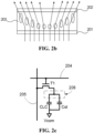
- FIG. 2b illustrates the sharing state of the anti-peep state switching film, the liquid crystals molecules regularly rotate, light extends through the film layer and exits along a diffuse direction, and the viewing angle is increased.
- FIG. 2c is an equivalent driver circuit diagram of the anti-peep state switching film and comprises a scan line 204, a data line 205 insulatively intersecting the scan line 204, and a thin film transistor T1 connected to the scan line 204 and the data line 205.
- a gate electrode of the thin film transistor T1 is connected to the scan line 204
- a source electrode of the thin film transistor T1 is connected to the data line 205
- a drain electrode of the thin film transistor T1 is connected to release electrodes 206.
- the release electrodes 206 and a common electrode Vcom form a difference of voltages and constitute a liquid crystal capacitor CLC and a storage capacitor Cst.
- the common electrode Vcom is located on any side of the anti-peep state switching film.
- the liquid crystal layer 203 of the anti-peep state switching film is made of non-PN type liquid crystals
- PN type liquid crystals are polymer network liquid crystals (PNLCs).
- PNLC liquid crystals are not spherical or ellipsoidal micro droplets, but are distributed in a three dimensional polymer net to form a continuous channel network.
- the PN type liquid crystals have two characteristics resulting in low contrast: 1)
- the anti-peep state switching film preferably employs a vertical alignment (VA) type liquid crystal film, a twisted nematic (TN) liquid crystal film, or an in-plane switching (IPSs) type liquid crystal film to guarantee display contrast of the liquid crystal display panel.
- VA vertical alignment
- TN twisted nematic
- IPSs in-plane switching
- the anti-peep state switching film can be divided into a middle region 302 and anti-peep regions 303 located on two sides of the middle region 302. Furthermore, a distribution sequence of the anti-peep region 303, the middle region 302, and the anti-peep region 303 is along a horizontal display direction of the liquid crystal display panel. An area of the anti-peep regions 303 is greater than an area of the middle region 302, and the areas of the anti-peep regions 303 located on the two sides of the middle region 302 are the same.
- An area of a single one of the anti-peep regions 303 is greater than an area of the middle region 302, and the greater the area of the single anti-peep regions 303 is, the smaller the area of the middle region 302 is.
- the middle region 302 has a viewing angle right facing a user, an non-right facing viewing angle does not allow a peep, which as a natural anti-peep effect.
- the anti-peep regions 303 on two sides are easily peeped by the suer, and an anti-peep process is required particularly. The greater the area of the anti-peep region 303 is, the wider the anti-peep viewing angle is and better the anti-peep effect is.
- a function of the anti-peep state switching film is direction-adjusting display light passing through the liquid crystal display panel.
- the anti-peep state refers that at a vertical viewing angle or approximately vertical viewing angle to the liquid crystal display panel, a better light transmittance is needed to fulfill normal information display and acquisition. On the contrary, at the angle departing from the vertical viewing angle, light needs to be blocked to reduce a display range to achieve an anti-peep effect. According to a requirement of viewing angle characteristics by the liquid crystal display panel under the anti-peep state, the driver electrodes of the anti-peep state switching film are required to be disposed separately.
- the release electrodes (electrodes disposed separately from one another) are disposed in an array on substrates of any sides of the anti-peep state switching film, adjacent ones of the release electrodes are disposed insulatively, each of the release electrodes drives liquid crystals of a corresponding region to rotate, and the release electrodes distributed on the entire anti-peep state switching film receives driving signals of different values through a time control to implement distinguishing rotation controls for the liquid crystals molecules of different regions to match the display requirement of the liquid crystal display panel in different viewing angles.
- an anti-peep state switching film takes a VA type anti-peep state switching film as an example for explanation.
- the anti-peep state switching film comprises a first substrate 304, a second substrate 305 disposed opposite to the first substrate 304, and a liquid crystal layer 306 disposed between the first substrate 304 and the second substrate 305.
- the driver electrodes are disposed on an upper side and a lower side of the liquid crystal layer 306.
- the driver electrodes comprise release electrodes 308 located on a side of the first substrate 304 facing the second substrate 305 and a common electrode 307 located on a side of the second substrate 305 facing the first substrate 304.
- the common electrode 307 and the release electrodes 308 are disposed oppositely and form a difference of voltages to drive the liquid crystals to rotate to change a display viewing angle of the liquid crystal display panel.
- the release electrodes are disposed separately on the first substrate 304 and/or the second substrate 305. Specifically, the release electrodes are disposed in array corresponding to the middle region 302 and the anti-peep regions 303 located on the two sides of the middle region 302. Driving voltage differences of regions (liquid crystal rotation is driven by a voltage difference between electrodes on upper and lower sides or left and right sides of the liquid crystals, the greater a voltage difference value is, the greater a rotational angle of the liquid crystals is) corresponding to different release electrodes are different. Rotational angles of the liquid crystals of the regions corresponding to the different release electrodes are different.
- driving voltage differences located in the middle region 302 and the anti-peep regions 303 are the same, and the rotational direction and angle of the liquid crystals of the corresponding regions are consistent to guide light to exit vertically out from the display panel such that the viewing angle can be lowered and the liquid crystals can be arranged along the same direction during alignment of the liquid crystals to achieve the anti-peep state without electrification.
- the driver electrodes of the regions corresponding to the different release electrodes drive the liquid crystals to rotate by different differences of the driving voltages, and the rotational angle of the liquid crystals of the anti-peep regions 303 is greater than the rotational angle of the liquid crystals of the middle region 302 to guide light to be diffusively emitted out to increase the viewing angle.
- the driver electrodes can be further refined along a vertical direction to improve a vertical display viewing angle.
- the driver electrodes comprise a common electrode 307 located on the first substrate 304 and release electrodes 308 located on the second substrate 305.
- the common electrode 307 is disposed on an entire surface, and the release electrodes 308 are distributed.
- the release electrodes 308 comprises strip electrodes D1-D15 disposed in an array along the horizontal display direction of the liquid crystal display panel, and adjacent ones of the strip electrodes are disposed parallelly at intervals.
- the strip electrodes are distributed in the middle region 302 and the anti-peep regions 303 on two sides of the middle region 302.
- the liquid crystal layer 306 of the anti-peep state switching film has been arranged regularly with a pre-tilt angle during alignment of the liquid crystals.
- a regular state is that long axes of the liquid crystals in the middle region 302 and the anti-peep regions 303 under the anti-peep state are along the same direction, the anti-peep state is maintained when no electrification is applied, and light is vertically emitted out from the display panel, which can lower the viewing angle.
- the common electrode 307 Under the sharing state, the common electrode 307 receives a constant voltage, the strip electrodes located in the middle region 302 and the anti-peep regions 303 a voltage different from that of the common electrode 307 to form a driving voltage difference to guide the liquid crystals to rotate according to the pre-tilt angle. In the meantime, a voltage difference between the strip electrodes located in the middle region 302 and the common electrode 307 is less than a voltage difference between the strip electrodes located in the anti-peep regions 303 and the common electrode 307 to further guide the liquid crystals in the anti-peep regions 303 to achieve large angle rotation, diffuse exiting light, and widen the display viewing angle.
- the anti-peep state switching film can be divided into a central region 309 and anti-peep regions 310 along a horizontal direction, a vertical direction and a diagonal display direction of the central region 309.
- An area of the anti-peep region 310 is greater than an area of the central region 309.
- the driver electrodes are evenly distributed in the central region 309 and the anti-peep regions 310 located on a periphery of the central region 309. Specifically, driving voltage differences of the regions corresponding to the different electrodes are different, rotational angles of the liquid crystals in different regions are different.
- difference of driving voltages in the central region 309 and the anti-peep regions 310 located on the periphery of the central region 309 are the same, and the rotation direction and angle of the liquid crystals in the regions corresponding to the electrodes are consistent to guide light to be vertically emitted out from the display panel such that the viewing angle can be lowered.
- the driver electrodes in regions corresponding to the different electrodes drive the liquid crystals to rotate by different differences of the driving voltages, and the rotational angle of the liquid crystals of the anti-peep regions 310 is greater than the rotational angle of the liquid crystals of the central region 309 to guide light to be diffusively emitted out to increase the viewing angle.
- the driver electrodes comprises a common electrode 307 located on the first substrate 304 and a release electrodes 308 located on the second substrate.
- the common electrode 307 is disposed as an entire surface, and the release electrodes 308 is distributed.
- the release electrodes 308 is annularly and radially disposed, the release electrodes 308 comprises a central electrode and annular electrodes extending outward from the central electrode.
- the central electrode is correspondingly located on a central display region of the liquid crystal display panel.
- the annular electrodes correspondingly covers the display region outside the central display region.
- the release electrodes 308 is annularly and radially disposed, for example, both the central electrode and the annular electrodes are hollow and circular electrode, and inner diameters of the annular electrodes gradually increase from a center of the anti-peep state switching film to an edge, and shapes of the annular electrodes extending outward gradually match an edge outline of the anti-peep state switching film.
- the strip electrodes Compared to the strip electrodes disposed in an array along a single direction, the strip electrodes only has the anti-peep effect along a single direction, namely, an display image is anti-peep along a horizontal direction or a vertical direction.
- the annular electrodes evenly distribute electrodes along the horizontal and vertical directions, different electrodes are distributed annularly on the entire anti-peep state switching film, and different electrodes also receive driving signals by a time control, which can achieve anti-peep and sharing on a periphery direction of the display panel.
- the liquid crystal layer 306 of the anti-peep state switching film has been arranged regularly with a pre-tilt angle and during alignment of the liquid crystals.
- a regular state is that the long axes of the liquid crystals in the central region 309 and the anti-peep regions 310 located on a periphery of the central region 309 are along the same direction under the anti-peep state, and the anti-peep state is maintained when no electrification is applied, and light is vertically emitted out from the display panel, which can lower the viewing angle.
- the common electrode 307 Under the sharing state, the common electrode 307 receives a constant voltage, the annular electrodes located in the central region 309 and the anti-peep regions 310 receives a voltage different from that on the common electrode 307 to form a driving voltage difference to guide the liquid crystals to rotate according to the pre-tilt angle.
- a voltage difference between the annular electrodes located in the central region 309 and the common electrode 307 is less than a voltage difference between the annular electrodes located in the anti-peep regions 310 and the common electrode 307 to further guide the liquid crystals of the anti-peep regions 310 to achieve large angle rotation, diffuse exiting light, and widen the display viewing angle.
- the anti-peep state switching film takes an IPS type as an example for explanation.
- the anti-peep state switching film comprises a first substrate 404, a second substrate disposed opposite to the first substrate 404, and a liquid crystal layer disposed between the first substrate 404 and the second substrate.
- Driver electrodes are disposed on a single side of the liquid crystal layer.
- the driver electrodes comprise a common electrode located on the first substrate 404, and release electrodes located on the same one of the first substrate and the second substrate with the common electrode, the common electrode and the release electrodes are-comb like and disposed alternately.
- the common electrode and the release electrodes constitute a horizontal electrical field to drive liquid crystals to rotate.
- the common electrode and the release electrodes can also be disposed on the second substrate, a liquid crystal driving principle and disposing are the same as those on the first substrate 404.
- the common electrode and the release electrodes are located on the same one of the first and second substrate, and the release electrodes comprise strip electrodes 402 disposed horizontally in an array on the first substrate 404.
- the common electrode comprises a comb electrode 403, and a common line 405 connected to the comb electrode 403.
- the strip electrodes 402 are embedded in a tooth electrode.
- the strip electrodes 402 have different driving voltages corresponding to the middle region and the anti-peep regions.
- the comb electrode 403 receives a constant voltage, and form a horizontal electrical field with adjacent one of the strip electrodes 402 to drive the liquid crystals to rotate. Voltage setting and embodying principles of the specific region are the same as those in the VA mode and will not be described repeatedly here.
- a driver IC on the substrate of the anti-peep state switching film disposed with the driver electrodes, a driver IC, a time control circuit connected to the driver IC, and a driving line connected to the time control circuit are disposed.
- the driving line comprises a gate electrode line disposed along a first direction, and a data line disposed along a second direction.
- the release electrodes are electrically connected to the gate electrode line and the data line through the thin film transistor.
- the anti-peep state switching films provided by the first embodiment and the second embodiment can achieve that the liquid crystal display panel displays under the anti-peep state or the sharing state.
- the anti-peep state switching film can also display under a comprehensive state.
- the anti-peep state switching film can predetermine a plurality of viewing angle modes to allow a user to select the modes as needed.
- the open anti-peep and sharing states process with regional anti-peep or sharing to the liquid crystal display panel, for example, sharing display images are only performed at a specific viewing angle, remaining display regions are in the anti-peep state.
- the specific viewing angle is not limited to a vertical viewing angle. Accordingly, a driving voltage of the strip electrodes of each region can be controlled individually to set angles for rotating the liquid crystals according to different requirements of viewing angles.
- an anti-peep state switching film driving method for a display device comprises: a first substrate and a second substrate disposed oppositely, a liquid crystal layer located between the first substrate and the second substrate, and driver electrodes located on at least one side of the liquid crystal layer, the driver electrodes comprise a common electrode and release electrodes disposed opposite to the common electrode, the release electrodes are distributed insulatively, and an electrical field is generated between the electrified release electrodes and the common electrode to drive the liquid crystals to rotate; wherein the driving method comprises: when the display device is in a sharing display mode, applying a current of a constant voltage to the common electrode of the anti-peep state switching film; and applying a voltage different from that on the common electrode to the release electrodes of the anti-peep state switching film to constitute an electrical field driving the liquid crystals to rotate, and voltages applied to adjacent ones of the release electrodes on the first substrate and the second substrate are different to diffuse rotational
- voltages applied to the release electrodes are gradually lowered along a direction from ones of the release electrodes relatively near a central display region to ones of the release electrodes relatively away from the central display region; and a minimal voltage value applied to the release electrodes is greater than or equal to a voltage value applied to the common electrode.
- the liquid crystals of the anti-peep state switching film are at a pre-tilt rotational angle, and the liquid crystals in a region corresponding to each of the release electrodes are at the same rotational angle to reduce a light exiting range.
- FIG. 5 is a time control diagram of the anti-peep state switching film under the sharing state
- the strip electrodes D1-D15 are disposed in an array
- voltages applied to adjacent ones of the strip electrodes are different, namely voltage differences between adjacent ones of the strip electrodes and the common electrode 307 are different
- a voltage difference between the strip electrode on an edge and the common electrode 307 is less than a voltage difference between the strip electrode in a middle and the common electrode 307.
- the voltage differences increase gradually from the edge to the middle. Therefore, voltage difference values of regions corresponding to adjacent ones of the strip electrodes are relatively even, a difference between rotational angles of the liquid crystals in different region is small, which can reduce poor display of alternating light and dark lines.
- the anti-peep state switching film can also be set to have the normal display as the sharing state, and switch to the anti-peep state after electrified to have a tilt state by aligning liquid crystals of the anti-peep state switching film, namely, the sharing state.
- the electrified liquid crystals rotate to the same direction, namely, the anti-peep state.
- the display device provided by present invention has an anti-peep display function and an anti-peep state switching film is further disposed on the display device.
- Selectively electrifying the anti-peep state switching film changes a display viewing angle of the display device to cooperate with anti-peep backlight to achieve switching of the anti-peep state and the sharing state at will such that application scenarios of the anti-peep display are more extensively.
Landscapes
- Physics & Mathematics (AREA)
- Nonlinear Science (AREA)
- Chemical & Material Sciences (AREA)
- Crystallography & Structural Chemistry (AREA)
- General Physics & Mathematics (AREA)
- Optics & Photonics (AREA)
- Mathematical Physics (AREA)
- Engineering & Computer Science (AREA)
- Microelectronics & Electronic Packaging (AREA)
- Liquid Crystal (AREA)
- Geometry (AREA)
- Liquid Crystal Display Device Control (AREA)
Abstract
Description
- The present application relates to a field of display technologies, especially to a display device with an anti-peep function and an anti-peep state switching film driving method thereof.
- With the development of network technologies, more and more people perform operations such as shopping or account transactions on the internet. Especially for demands of banks and government security agencies, during the above operations, operators often need to input personal information to display devices of computers, mobile phones, ATMs, and automatic ticket dispensers, which can easily cause leakage of personal information. Therefore, an anti-peep capability of a display device is getting more and more attention.
- With anti-peep technologies of liquid crystal displays (LCDs) gradually maturing, more and more anti-peep products emerge. Namely, by adding an advance light control film (ALCF) in a backlight to control a light exiting viewing angle of the backlight, an anti-peep display is visible within a certain small viewing angle, and displayed imaged cannot be viewed in a large viewing angle, which performs an anti-peep effect.
- Conventional anti-peep displays bring users excellent privacy. The anti-peep displays are intensively used in personal information display devices in public places but an anti-peep function cannot be switched to a sharing state, which makes use scenarios and use functions limited and a market value thereof is difficult the exert. For example, display devices used for meeting rooms can switch to an anti-peep state according to use scenarios. When a confidential meeting is proceeded, the display device can switch on the anti-peep state to reduce a viewing angle. When training a groupd of people is needed, a larger display viewing angle is required to meet the needs of viewers in different locations to clearly view the display contents.
- As described above, the conventional anti-peep display device function are relatively simple functions and cannot switch the anti-peep state. It is required to provide a display device that can switch a display effect of a anti-peep state or a sharing state according to use scenarios to fill a market gap.
- The present application embodiment provides a display device and an anti-peep state switching film driving method thereof to solve a technical issue that a conventional anti-peep display device only has an anti-peep state and cannot select the anti-peep state or a sharing state according to application scenarios.
- To solve the above technical issue, the present invention provides a display device capable of switching an anti-peep state, comprising:
- a liquid crystal display panel;
- an anti-peep film located on a light incident side of the liquid crystal display panel and configured to achieve anti-peep display; and,
- an anti-peep state switching film located on a light exiting side of the liquid crystal display panel and configured to achieve switching between display effects of an anti-peep state and a sharing state;
- wherein the anti-peep state switching film comprises:
- a first substrate and a second substrate disposed oppositely, a liquid crystal layer located between the first substrate and the second substrate, and driver electrodes located on at least one side of the liquid crystal layer, wherein the driver electrodes are configured to drive liquid crystals of the liquid crystal layer to rotate to adjust a light exiting angle of display light;
- when the liquid crystal display panel is in the anti-peep state, the driver electrodes of the anti-peep state switching film drive the liquid crystals in a region corresponding to each of electrodes to rotate relative to the first and second substrates by the same angle to reduce the light exiting angle of display light; or, after the liquid crystal display panel switches to the sharing state, the driver electrodes drive the liquid crystals in a region corresponding each of electrodes to rotate relative to the first and second substrates by different angles to diffuse the light exiting angle of display light.
- According to a preferred embodiment of the present invention, the anti-peep state switching film comprises a middle region and anti-peep regions located on a central region along a horizontal display direction, a vertical display direction, and a diagonal display direction, and an area of the anti-peep regions is greater than an area of the central region.
- According to a preferred embodiment of the present invention, the driver electrodes are distributed on the central region and the anti-peep regions located on a periphery of the central region, a difference of driving voltages of each of the driver electrodes corresponding to the central region and the anti-peep regions respectively is different from that of another of the driver electrodes, and rotational angles of the liquid crystals in the central region and the anti-peep regions respectively are different.
- According to a preferred embodiment of the present invention, when the liquid crystal display panel is in the anti-peep state, the difference of the driving voltages located in the central region is the same as the difference of the driving voltages located in the anti-peep regions on the periphery of the central region;
when the liquid crystal display panel is in the sharing state, the driver electrodes in regions corresponding to the different electrodes drive the liquid crystals to rotate by different differences of the driving voltages, and the rotational angle of the liquid crystals of the anti-peep regions is greater than the rotational angle of the liquid crystals of the central region. - According to a preferred embodiment of the present invention, the driver electrodes comprise a common electrode located on the first substrate or the second substrate, and release electrodes relatively located on the other of the first substrate and the second substrate, wherein the common electrode is disposed as an entire surface, the release electrodes are arranged in an array, and adjacent ones of the release electrodes are insulative to each other to individually receive a time signal, the common electrode and the release electrodes are electrified to constitute a vertical electrical field.
- According to a preferred embodiment of the present invention, the release electrodes comprise strip electrodes arranged in an array along a horizontal display direction of the liquid crystal display panel, adjacent ones of the strip electrodes are disposed at an interval, and the strip electrodes are correspondingly distributed on a middle display region and a display region relatively located on two sides of the middle display region.
- According to a preferred embodiment of the present invention, the release electrodes is annularly and radially disposed, the release electrodes comprise a central electrode pattern, and annular electrode patterns extending outward from the central electrode pattern, the central electrode pattern is correspondingly located in a central display region of the liquid crystal display panel, and the annular electrode patterns correspondingly covers the display region outside the central display region.
- According to a preferred embodiment of the present invention, the central electrode and the annular electrodes are hollow and circular electrodes, and inner diameters of the annular electrodes gradually increase from a center of the anti-peep state switching film to an edge, and shapes of the annular electrodes extending outward gradually fit an edge outline of the anti-peep state switching film.
- According to a preferred embodiment of the present invention, on a side of the anti-peep state switching film disposed with the release electrodes, a driver integrated circuit (IC), a time control circuit connected to the driver IC, and a driving line connected to the time control circuit are disposed, the driving line comprises a gate electrode line disposed along a first direction and a data line disposed along second direction, and the release electrodes are electrically connected the gate electrode line and the data line through thin film transistors.
- According to a preferred embodiment of the present invention, the display device further comprises a scan line, a data line insulatively intersecting the scan line, and a thin film transistor connected to the scan line and the data line, a gate electrode of the thin film transistor is connected to the scan line, a source electrode is connected to the data line, a drain electrode is connected to release electrodes, the release electrodes and the common electrode form a difference of voltages constitute a liquid crystal capacitor and a storage capacitor.
- According to a preferred embodiment of the present invention, the anti-peep state switching film comprises a middle region and anti-peep regions located on two sides of the middle region, and a distribution sequence of the anti-peep region, the middle region, and the anti-peep region is along a horizontal display direction of the liquid crystal display panel; and
an area of the anti-peep regions is greater than an area of the middle region, and areas of the anti-peep regions on the two sides of the middle region are the same. - According to a preferred embodiment of the present invention, the driver electrodes comprise a common electrode located on the first substrate or the second substrate and release electrodes located on the same one of the first substrate and the second substrate with the common electrode, wherein the common electrode is disposed in a comb shape, the release electrodes are disposed insulatively to one another and arranged in an array to individually receive a time signal, the release electrodes are correspondingly disposed in gaps of the common electrode, and the common electrode and the release electrodes are electrified to constitute a horizontal electrical field.
- According to a preferred embodiment of the present invention, the release electrodes comprise strip electrodes arranged in an array along the horizontal display direction of the liquid crystal display panel, the common electrode comprises a comb electrode and a common line connected to the comb electrode, and the strip electrodes are embedded in a tooth electrode formed by the comb electrode and the common line.
- According to a preferred embodiment of the present invention, a driving voltage of the strip electrodes corresponding to the middle region and a driving voltage of the corresponding to the anti-peep regions are different, the comb electrode receives a constant voltage, and the comb electrode and adjacent one of the strip electrodes form a horizontal electrical field to drive the liquid crystals to rotate.
- According to a preferred embodiment of the present invention, a backlight module is further disposed on the light incident side of the liquid crystal display panel, and the backlight module comprises:
- a light guide plate;
- a light source located on a light incident side of the light guide plate;
- a diffuser plate located on a light exiting side of the light guide plate;
- a prism film located on a light exiting side of the diffuser plate; and,
- the anti-peep film located on a light exiting side of the prism film.
- According to a preferred embodiment of the present invention, the anti-peep film is a microscopic shutter, and an interval of the microscopic shutter is 0.07mm.
- According to a preferred embodiment of the present invention, the liquid crystal layer is one of vertically rotational type liquid crystals, twisted nematic type liquid crystals, or horizontally rotational type liquid crystals.
- According to the display device provided by the present invention, also provides an anti-peep state switching film driving method for a display device, an anti-peep state switching film comprises: a first substrate and a second substrate disposed oppositely, a liquid crystal layer located between the first substrate and the second substrate, and driver electrodes located on at least one side of the liquid crystal layer, the driver electrodes comprise a common electrode and release electrodes disposed opposite to the common electrode, the release electrodes are distributed insulatively, and an electrical field is generated between the electrified release electrodes and the common electrode to drive the liquid crystals to rotate;
wherein the driving method comprises: - when the display device is in a sharing display mode, applying a current of a constant voltage to the common electrode of the anti-peep state switching film; and
- applying a voltage different from that on the common electrode to the release electrodes of the anti-peep state switching film to constitute an electrical field driving the liquid crystals to rotate, and voltages applied to adjacent ones of the release electrodes on the first substrate and the second substrate are different to diffuse rotational angles of the liquid crystals.
- According to a preferred embodiment of the present invention, the method further comprises:
- in the release electrodes distributed on the first substrate or the second substrate, voltages applied to the release electrodes are gradually lowered along a direction from ones of the release electrodes relatively near a central display region to ones of the release electrodes relatively away from the central display region; and
- a minimal voltage value applied to the release electrodes is greater than or equal to a voltage value applied to the common electrode.
- According to a preferred embodiment of the present invention, when the display device is in an anti-peep display mode, no voltage is applied to the anti-peep state switching film, the liquid crystals of the anti-peep state switching film are at a pre-tilt rotational angle, and the liquid crystals in a region corresponding to each of the release electrodes are at the same rotational angle to reduce a light exiting range.
- Advantages of the present application embodiment are as follows: Compare to the conventional technology, the present invention provides a display device and an anti-peep state switching film driving method thereof. The display device has an anti-peep display function, and an anti-peep state switching film is also disposed on the display device. Selectively electrifying the anti-peep state switching film can change a display viewing angle of the display device. Specifically, a time control cooperatively supplies each of the release electrodes with a driving signal individually to achieve switching between an anti-peep state and a sharing state at will such that application scenarios of the anti-peep display becomes more extensive.
-
-
FIG. 1 is a schematic structural view of a display device provided by the present invention; -
FIGs. 2a and2b are schematic principle views of anti-peep state switching of the display device provided by the present invention; -
FIG. 2c is a view of a driver circuit of an anti-peep state switching film of a display device provided by the present invention; -
FIGs. 3a to 3d are schematic structural views of a first embodiment of the display device provided by the present invention; -
FIG. 4 is a schematic structural view of a second embodiment of the display device provided by the present invention; and -
FIG. 5 is a driving principle timing diagram of switching of an anti-peep state of the display device provided by the present invention. - The present application provides a display device with an anti-peep function and an anti-peep state switching film driving method thereof. To make the objective, the technical solution, and the effect of the present application clearer and more explicit, the present application will be further described in detail below with reference to the accompanying drawings. It should be understood that the specific embodiments described here are only used to explain the present application instead of being used to limit the present application.
- Further descriptions of the present application in conjunction with the drawings and specific embodiments are as follows.
- The present application embodiment provides a display device including an anti-peep function, and detailed descriptions in conjunction with
FIGs. 1 to 4 are as follows. - With reference to
FIG. 1, FIG. 1 illustrates the display device provided by the present invention comprising a liquidcrystal display panel 101, a backlight module and ananti-peep film 102 located on a light incident side of the liquidcrystal display panel 101, and an anti-peepstate switching film 103 located on a light exiting side of the liquidcrystal display panel 101. The backlight module comprises alight guide plate 104, a light source located on a light incident side of thelight guide plate 104, adiffuser plate 105 located on a light exiting side of thelight guide plate 104, and aprism film 106 located on a light exiting side of thediffuser plate 105. Theanti-peep film 102 is located on a light exiting side of theprism film 106. - The
anti-peep film 102 is disposed between the backlight module and the liquidcrystal display panel 101 and is configured to filter partial backlight entering the liquidcrystal display panel 101 into a light in an specific angle. Theanti-peep film 102 exists in form of a microscopic shutter. An interval of the microscopic shutter is 0.07mm, and a fence of the microscopic shutter has a certain height and can absorb and limit passing light in the viewing angle. Generally, a right viewing angle serves as a normal, a viewing angle of light of theanti-peep film 102 can be 60±4 degrees. - The anti-peep
state switching film 103 is disposed on the light exiting side of the liquidcrystal display panel 101. The anti-peepstate switching film 103 also serves as a light filtering layer and can adjust an angle of exiting light of the liquidcrystal display panel 101, which not only achieves a sharing state of a large viewing angle, but also achieves a anti-peep state of a small viewing angle. - With reference to
FIGs. 2a and2b ,FIGs 2a and2b are schematic structural views of the anti-peep state switching film, and the anti-peep state switching film comprises afirst substrate 201, asecond substrate 202 disposed opposite to thefirst substrate 201, aliquid crystal layer 203 located between thefirst substrate 201 and thesecond substrate 202, and driver electrodes located on at least one side of theliquid crystal layer 203. A driving principle of theliquid crystal layer 203 of the anti-peep state switching film is similar to a driving principle of the liquid crystal display panel, both are generating a vertical electrical field or a horizontal electrical field through the driver electrodes to drive the liquid crystals to rotate to adjust light of transmission light to further adjust a viewing angle of the liquid crystal display panel. A difference is that control of theliquid crystal layer 203 of the liquid crystal display panel is specifically in a pixel level so densities of metal wiring and driver electrode arrangement is high and precision requirement is high. Control precision of the anti-peep state switching film is specifically to display partitions, its manufacturing precision requirement is comparatively low, and a manufacturing cost thereof is low. Specifically, taking a VA type liquid crystal mode for example,FIG. 2a illustrates the anti-peep state of the anti-peep state switching film, liquid crystals molecules are neatly arranged without rotation, and light extends through theliquid crystal layer 203 and exits along a vertical direction, the viewing angle is lower. On the contrary,FIG. 2b illustrates the sharing state of the anti-peep state switching film, the liquid crystals molecules regularly rotate, light extends through the film layer and exits along a diffuse direction, and the viewing angle is increased. - With reference to
FIG. 2c, FIG. 2c is an equivalent driver circuit diagram of the anti-peep state switching film and comprises ascan line 204, adata line 205 insulatively intersecting thescan line 204, and a thin film transistor T1 connected to thescan line 204 and thedata line 205. A gate electrode of the thin film transistor T1 is connected to thescan line 204, a source electrode of the thin film transistor T1 is connected to thedata line 205, and a drain electrode of the thin film transistor T1 is connected to releaseelectrodes 206. Therelease electrodes 206 and a common electrode Vcom form a difference of voltages and constitute a liquid crystal capacitor CLC and a storage capacitor Cst. The common electrode Vcom is located on any side of the anti-peep state switching film. - Specifically, the
liquid crystal layer 203 of the anti-peep state switching film is made of non-PN type liquid crystals, PN type liquid crystals are polymer network liquid crystals (PNLCs). PNLC liquid crystals are not spherical or ellipsoidal micro droplets, but are distributed in a three dimensional polymer net to form a continuous channel network. The PN type liquid crystals have two characteristics resulting in low contrast: 1) The PNLC has a high cell thickness (10um/16um), a transmittance Tr=2Φ, the cell thickness of the PNLC is greater so the PNLC is brighter in a dark state, which affects contrast, and the contrast is a ratio of a bright state to the dark state. 2) Alignment conditions of the PNLC liquid crystals require ultra-low temperature processes and high energy irradiation, because a temperature difference between portions of the substrate, alignment effect is poor to affect a dark state effect. As above, the PN type liquid crystals would lead to low contrast of the liquid crystal display panel. The anti-peep state switching film preferably employs a vertical alignment (VA) type liquid crystal film, a twisted nematic (TN) liquid crystal film, or an in-plane switching (IPSs) type liquid crystal film to guarantee display contrast of the liquid crystal display panel. - With reference to
FIG. 3a , the anti-peep state switching film, according to viewing angle requirements of the liquid crystal display panel, can be divided into amiddle region 302 andanti-peep regions 303 located on two sides of themiddle region 302. Furthermore, a distribution sequence of theanti-peep region 303, themiddle region 302, and theanti-peep region 303 is along a horizontal display direction of the liquid crystal display panel. An area of theanti-peep regions 303 is greater than an area of themiddle region 302, and the areas of theanti-peep regions 303 located on the two sides of themiddle region 302 are the same. An area of a single one of theanti-peep regions 303 is greater than an area of themiddle region 302, and the greater the area of the singleanti-peep regions 303 is, the smaller the area of themiddle region 302 is. themiddle region 302 has a viewing angle right facing a user, an non-right facing viewing angle does not allow a peep, which as a natural anti-peep effect. However, theanti-peep regions 303 on two sides are easily peeped by the suer, and an anti-peep process is required particularly. The greater the area of theanti-peep region 303 is, the wider the anti-peep viewing angle is and better the anti-peep effect is. - A function of the anti-peep state switching film is direction-adjusting display light passing through the liquid crystal display panel. In combination with actual use scenarios, the anti-peep state refers that at a vertical viewing angle or approximately vertical viewing angle to the liquid crystal display panel, a better light transmittance is needed to fulfill normal information display and acquisition. On the contrary, at the angle departing from the vertical viewing angle, light needs to be blocked to reduce a display range to achieve an anti-peep effect. According to a requirement of viewing angle characteristics by the liquid crystal display panel under the anti-peep state, the driver electrodes of the anti-peep state switching film are required to be disposed separately. Namely, the release electrodes (electrodes disposed separately from one another) are disposed in an array on substrates of any sides of the anti-peep state switching film, adjacent ones of the release electrodes are disposed insulatively, each of the release electrodes drives liquid crystals of a corresponding region to rotate, and the release electrodes distributed on the entire anti-peep state switching film receives driving signals of different values through a time control to implement distinguishing rotation controls for the liquid crystals molecules of different regions to match the display requirement of the liquid crystal display panel in different viewing angles.
- With reference to
FIGs. 3a and 3b , an anti-peep state switching film provided by the present invention takes a VA type anti-peep state switching film as an example for explanation. Specifically, the anti-peep state switching film comprises afirst substrate 304, asecond substrate 305 disposed opposite to thefirst substrate 304, and aliquid crystal layer 306 disposed between thefirst substrate 304 and thesecond substrate 305. The driver electrodes are disposed on an upper side and a lower side of theliquid crystal layer 306. The driver electrodes compriserelease electrodes 308 located on a side of thefirst substrate 304 facing thesecond substrate 305 and acommon electrode 307 located on a side of thesecond substrate 305 facing thefirst substrate 304. Thecommon electrode 307 and therelease electrodes 308 are disposed oppositely and form a difference of voltages to drive the liquid crystals to rotate to change a display viewing angle of the liquid crystal display panel. - The release electrodes are disposed separately on the
first substrate 304 and/or thesecond substrate 305. Specifically, the release electrodes are disposed in array corresponding to themiddle region 302 and theanti-peep regions 303 located on the two sides of themiddle region 302. Driving voltage differences of regions (liquid crystal rotation is driven by a voltage difference between electrodes on upper and lower sides or left and right sides of the liquid crystals, the greater a voltage difference value is, the greater a rotational angle of the liquid crystals is) corresponding to different release electrodes are different. Rotational angles of the liquid crystals of the regions corresponding to the different release electrodes are different. For example, under the anti-peep state, driving voltage differences located in themiddle region 302 and theanti-peep regions 303 are the same, and the rotational direction and angle of the liquid crystals of the corresponding regions are consistent to guide light to exit vertically out from the display panel such that the viewing angle can be lowered and the liquid crystals can be arranged along the same direction during alignment of the liquid crystals to achieve the anti-peep state without electrification. Also, for example, under the sharing state, the driver electrodes of the regions corresponding to the different release electrodes drive the liquid crystals to rotate by different differences of the driving voltages, and the rotational angle of the liquid crystals of theanti-peep regions 303 is greater than the rotational angle of the liquid crystals of themiddle region 302 to guide light to be diffusively emitted out to increase the viewing angle. - In the present embodiment, under the sharing state, the display viewing angle is greater along a horizontal direction, the driver electrodes can be further refined along a vertical direction to improve a vertical display viewing angle.
- The driver electrodes comprise a
common electrode 307 located on thefirst substrate 304 and releaseelectrodes 308 located on thesecond substrate 305. Thecommon electrode 307 is disposed on an entire surface, and therelease electrodes 308 are distributed. Furthermore, therelease electrodes 308 comprises strip electrodes D1-D15 disposed in an array along the horizontal display direction of the liquid crystal display panel, and adjacent ones of the strip electrodes are disposed parallelly at intervals. The strip electrodes are distributed in themiddle region 302 and theanti-peep regions 303 on two sides of themiddle region 302. - Specifically, the
liquid crystal layer 306 of the anti-peep state switching film has been arranged regularly with a pre-tilt angle during alignment of the liquid crystals. A regular state is that long axes of the liquid crystals in themiddle region 302 and theanti-peep regions 303 under the anti-peep state are along the same direction, the anti-peep state is maintained when no electrification is applied, and light is vertically emitted out from the display panel, which can lower the viewing angle. Under the sharing state, thecommon electrode 307 receives a constant voltage, the strip electrodes located in themiddle region 302 and the anti-peep regions 303 a voltage different from that of thecommon electrode 307 to form a driving voltage difference to guide the liquid crystals to rotate according to the pre-tilt angle. In the meantime, a voltage difference between the strip electrodes located in themiddle region 302 and thecommon electrode 307 is less than a voltage difference between the strip electrodes located in theanti-peep regions 303 and thecommon electrode 307 to further guide the liquid crystals in theanti-peep regions 303 to achieve large angle rotation, diffuse exiting light, and widen the display viewing angle. - With reference to
FIG. 3c , the anti-peep state switching film, according to viewing angle requirements of the liquid crystal display panel, can be divided into acentral region 309 andanti-peep regions 310 along a horizontal direction, a vertical direction and a diagonal display direction of thecentral region 309. An area of theanti-peep region 310 is greater than an area of thecentral region 309. the driver electrodes are evenly distributed in thecentral region 309 and theanti-peep regions 310 located on a periphery of thecentral region 309. Specifically, driving voltage differences of the regions corresponding to the different electrodes are different, rotational angles of the liquid crystals in different regions are different. For example, under the anti-peep state, difference of driving voltages in thecentral region 309 and theanti-peep regions 310 located on the periphery of thecentral region 309 are the same, and the rotation direction and angle of the liquid crystals in the regions corresponding to the electrodes are consistent to guide light to be vertically emitted out from the display panel such that the viewing angle can be lowered. Also for example, under the sharing state, the driver electrodes in regions corresponding to the different electrodes drive the liquid crystals to rotate by different differences of the driving voltages, and the rotational angle of the liquid crystals of theanti-peep regions 310 is greater than the rotational angle of the liquid crystals of thecentral region 309 to guide light to be diffusively emitted out to increase the viewing angle. - With reference to
FIG. 3d , the driver electrodes comprises acommon electrode 307 located on thefirst substrate 304 and arelease electrodes 308 located on the second substrate. Thecommon electrode 307 is disposed as an entire surface, and therelease electrodes 308 is distributed. Furthermore, therelease electrodes 308 is annularly and radially disposed, therelease electrodes 308 comprises a central electrode and annular electrodes extending outward from the central electrode. The central electrode is correspondingly located on a central display region of the liquid crystal display panel. The annular electrodes correspondingly covers the display region outside the central display region. - The
release electrodes 308 is annularly and radially disposed, for example, both the central electrode and the annular electrodes are hollow and circular electrode, and inner diameters of the annular electrodes gradually increase from a center of the anti-peep state switching film to an edge, and shapes of the annular electrodes extending outward gradually match an edge outline of the anti-peep state switching film. Compared to the strip electrodes disposed in an array along a single direction, the strip electrodes only has the anti-peep effect along a single direction, namely, an display image is anti-peep along a horizontal direction or a vertical direction. The annular electrodes evenly distribute electrodes along the horizontal and vertical directions, different electrodes are distributed annularly on the entire anti-peep state switching film, and different electrodes also receive driving signals by a time control, which can achieve anti-peep and sharing on a periphery direction of the display panel. - Specifically, with reference to
FIGs. 3b to 3d , theliquid crystal layer 306 of the anti-peep state switching film has been arranged regularly with a pre-tilt angle and during alignment of the liquid crystals. A regular state is that the long axes of the liquid crystals in thecentral region 309 and theanti-peep regions 310 located on a periphery of thecentral region 309 are along the same direction under the anti-peep state, and the anti-peep state is maintained when no electrification is applied, and light is vertically emitted out from the display panel, which can lower the viewing angle. Under the sharing state, thecommon electrode 307 receives a constant voltage, the annular electrodes located in thecentral region 309 and theanti-peep regions 310 receives a voltage different from that on thecommon electrode 307 to form a driving voltage difference to guide the liquid crystals to rotate according to the pre-tilt angle. In the meantime, a voltage difference between the annular electrodes located in thecentral region 309 and thecommon electrode 307 is less than a voltage difference between the annular electrodes located in theanti-peep regions 310 and thecommon electrode 307 to further guide the liquid crystals of theanti-peep regions 310 to achieve large angle rotation, diffuse exiting light, and widen the display viewing angle. - With reference to
FIG. 4 , the anti-peep state switching film provided by the present invention takes an IPS type as an example for explanation. Specifically, the anti-peep state switching film comprises afirst substrate 404, a second substrate disposed opposite to thefirst substrate 404, and a liquid crystal layer disposed between thefirst substrate 404 and the second substrate. Driver electrodes are disposed on a single side of the liquid crystal layer. The driver electrodes comprise a common electrode located on thefirst substrate 404, and release electrodes located on the same one of the first substrate and the second substrate with the common electrode, the common electrode and the release electrodes are-comb like and disposed alternately. The common electrode and the release electrodes constitute a horizontal electrical field to drive liquid crystals to rotate. Similarly, the common electrode and the release electrodes can also be disposed on the second substrate, a liquid crystal driving principle and disposing are the same as those on thefirst substrate 404. - Specifically, the common electrode and the release electrodes are located on the same one of the first and second substrate, and the release electrodes comprise
strip electrodes 402 disposed horizontally in an array on thefirst substrate 404. The common electrode comprises acomb electrode 403, and acommon line 405 connected to thecomb electrode 403. Thestrip electrodes 402 are embedded in a tooth electrode. - Similarly, the
strip electrodes 402 have different driving voltages corresponding to the middle region and the anti-peep regions. Thecomb electrode 403 receives a constant voltage, and form a horizontal electrical field with adjacent one of thestrip electrodes 402 to drive the liquid crystals to rotate. Voltage setting and embodying principles of the specific region are the same as those in the VA mode and will not be described repeatedly here. - Combining the first embodiment and second embodiment, on the substrate of the anti-peep state switching film disposed with the driver electrodes, a driver IC, a time control circuit connected to the driver IC, and a driving line connected to the time control circuit are disposed. The driving line comprises a gate electrode line disposed along a first direction, and a data line disposed along a second direction. The release electrodes are electrically connected to the gate electrode line and the data line through the thin film transistor.
- The anti-peep state switching films provided by the first embodiment and the second embodiment can achieve that the liquid crystal display panel displays under the anti-peep state or the sharing state. On such basis, the anti-peep state switching film can also display under a comprehensive state. For example, the anti-peep state switching film can predetermine a plurality of viewing angle modes to allow a user to select the modes as needed. Namely, the open anti-peep and sharing states process with regional anti-peep or sharing to the liquid crystal display panel, for example, sharing display images are only performed at a specific viewing angle, remaining display regions are in the anti-peep state. The specific viewing angle is not limited to a vertical viewing angle. Accordingly, a driving voltage of the strip electrodes of each region can be controlled individually to set angles for rotating the liquid crystals according to different requirements of viewing angles.
- According to the display device provided by the present invention, an anti-peep state switching film driving method for a display device is further provided, the anti-peep state switching film comprises: a first substrate and a second substrate disposed oppositely, a liquid crystal layer located between the first substrate and the second substrate, and driver electrodes located on at least one side of the liquid crystal layer, the driver electrodes comprise a common electrode and release electrodes disposed opposite to the common electrode, the release electrodes are distributed insulatively, and an electrical field is generated between the electrified release electrodes and the common electrode to drive the liquid crystals to rotate; wherein the driving method comprises: when the display device is in a sharing display mode, applying a current of a constant voltage to the common electrode of the anti-peep state switching film; and applying a voltage different from that on the common electrode to the release electrodes of the anti-peep state switching film to constitute an electrical field driving the liquid crystals to rotate, and voltages applied to adjacent ones of the release electrodes on the first substrate and the second substrate are different to diffuse rotational angles of the liquid crystals.
- Furthermore, in the release electrodes distributed on the first substrate or the second substrate, voltages applied to the release electrodes are gradually lowered along a direction from ones of the release electrodes relatively near a central display region to ones of the release electrodes relatively away from the central display region; and a minimal voltage value applied to the release electrodes is greater than or equal to a voltage value applied to the common electrode.
- Furthermore, when the display device is in an anti-peep display mode, no voltage is applied to the anti-peep state switching film, the liquid crystals of the anti-peep state switching film are at a pre-tilt rotational angle, and the liquid crystals in a region corresponding to each of the release electrodes are at the same rotational angle to reduce a light exiting range.
- With reference to
FIG. 5, FIG. 5 is a time control diagram of the anti-peep state switching film under the sharing state, the strip electrodes D1-D15 are disposed in an array, voltages applied to adjacent ones of the strip electrodes are different, namely voltage differences between adjacent ones of the strip electrodes and thecommon electrode 307 are different, and a voltage difference between the strip electrode on an edge and thecommon electrode 307 is less than a voltage difference between the strip electrode in a middle and thecommon electrode 307. The voltage differences increase gradually from the edge to the middle. Therefore, voltage difference values of regions corresponding to adjacent ones of the strip electrodes are relatively even, a difference between rotational angles of the liquid crystals in different region is small, which can reduce poor display of alternating light and dark lines. - The above solution description is for normal display of the anti-peep state switching film in the anti-peep state, and the anti-peep state switching film switches to the sharing state after electrified. Similarly, the anti-peep state switching film can also be set to have the normal display as the sharing state, and switch to the anti-peep state after electrified to have a tilt state by aligning liquid crystals of the anti-peep state switching film, namely, the sharing state. On the contrary, the electrified liquid crystals rotate to the same direction, namely, the anti-peep state. Two driving ways and setting principles are the same and will not be described repeatedly here.
- Compare to the conventional technology, the display device provided by present invention has an anti-peep display function and an anti-peep state switching film is further disposed on the display device. Selectively electrifying the anti-peep state switching film changes a display viewing angle of the display device to cooperate with anti-peep backlight to achieve switching of the anti-peep state and the sharing state at will such that application scenarios of the anti-peep display are more extensively.
- Although the preferred embodiments of the present invention have been disclosed as above, the aforementioned preferred embodiments are not used to limit the present invention. The person of ordinary skill in the art may make various changes and modifications without departing from the spirit and scope of the present invention. Therefore, the scope of protection of the present invention is defined by the scope of the claims.
Claims (20)
- A display device, comprising:a liquid crystal display panel;an anti-peep film located on a light incident side of the liquid crystal display panel and configured to achieve anti-peep display; and,an anti-peep state switching film located on a light exiting side of the liquid crystal display panel and configured to achieve switching between display effects of an anti-peep state and a sharing state;wherein the anti-peep state switching film comprises:a first substrate and a second substrate disposed oppositely, a liquid crystal layer located between the first substrate and the second substrate, and driver electrodes located on at least one side of the liquid crystal layer, wherein the driver electrodes are configured to drive liquid crystals of the liquid crystal layer to rotate to adjust a light exiting angle of display light;when the liquid crystal display panel is in the anti-peep state, the driver electrodes of the anti-peep state switching film drive the liquid crystals in a region corresponding to each of electrodes to rotate relative to the first and second substrates by the same angle to reduce the light exiting angle of display light; or, after the liquid crystal display panel switches to the sharing state, the driver electrodes drive the liquid crystals in a region corresponding each of electrodes to rotate relative to the first and second substrates by different angles to diffuse the light exiting angle of display light.
- The display device according to claim 1, wherein the anti-peep state switching film comprises a middle region and anti-peep regions located on a central region along a horizontal display direction, a vertical display direction, and a diagonal display direction, and an area of the anti-peep regions is greater than an area of the central region.
- The display device according to claim 2, wherein the driver electrodes are distributed on the central region and the anti-peep regions located on a periphery of the central region, a difference of driving voltages of each of the driver electrodes corresponding to the central region and the anti-peep regions respectively is different from that of another of the driver electrodes, and rotational angles of the liquid crystals in the central region and the anti-peep regions respectively are different.
- The display device according to claim 3, wherein when the liquid crystal display panel is in the anti-peep state, the difference of the driving voltages located in the central region is the same as the difference of the driving voltages located in the anti-peep regions on the periphery of the central region;
when the liquid crystal display panel is in the sharing state, the driver electrodes in regions corresponding to the different electrodes drive the liquid crystals to rotate by different differences of the driving voltages, and the rotational angle of the liquid crystals of the anti-peep regions is greater than the rotational angle of the liquid crystals of the central region. - The display device according to claim 4, wherein the driver electrodes comprise a common electrode located on the first substrate or the second substrate, and release electrodes relatively located on the other of the first substrate and the second substrate, wherein the common electrode is disposed as an entire surface, the release electrodes are arranged in an array, and adjacent ones of the release electrodes are insulative to each other to individually receive a time signal, the common electrode and the release electrodes are electrified to constitute a vertical electrical field.
- The display device according to claim 5, wherein the release electrodes comprise strip electrodes arranged in an array along a horizontal display direction of the liquid crystal display panel, adjacent ones of the strip electrodes are disposed at an interval, and the strip electrodes are correspondingly distributed on a middle display region and a display region relatively located on two sides of the middle display region.
- The display device according to claim 6, wherein the release electrodes is annularly and radially disposed, the release electrodes comprise a central electrode pattern, and annular electrode patterns extending outward from the central electrode pattern, the central electrode pattern is correspondingly located in a central display region of the liquid crystal display panel, and the annular electrode patterns correspondingly covers the display region outside the central display region.
- The display device according to claim 7, wherein the central electrode and the annular electrodes are hollow and circular electrodes, and inner diameters of the annular electrodes gradually increase from a center of the anti-peep state switching film to an edge, and shapes of the annular electrodes extending outward gradually fit an edge outline of the anti-peep state switching film.
- The display device according to claim 5, wherein on a side of the anti-peep state switching film disposed with the release electrodes, a driver integrated circuit (IC), a time control circuit connected to the driver IC, and a driving line connected to the time control circuit are disposed, the driving line comprises a gate electrode line disposed along a first direction and a data line disposed along second direction, and the release electrodes are electrically connected the gate electrode line and the data line through thin film transistors.
- The display device according to claim 5, wherein the display device further comprises a scan line, a data line insulatively intersecting the scan line, and a thin film transistor connected to the scan line and the data line, a gate electrode of the thin film transistor is connected to the scan line, a source electrode is connected to the data line, a drain electrode is connected to release electrodes, the release electrodes and the common electrode form a difference of voltages constitute a liquid crystal capacitor and a storage capacitor.
- The display device according to claim 1, wherein the anti-peep state switching film comprises a middle region and anti-peep regions located on two sides of the middle region, and a distribution sequence of the anti-peep region, the middle region, and the anti-peep region is along a horizontal display direction of the liquid crystal display panel; and
an area of the anti-peep regions is greater than an area of the middle region, and areas of the anti-peep regions on the two sides of the middle region are the same. - The display device according to claim 11, wherein the driver electrodes comprise a common electrode located on the first substrate or the second substrate and release electrodes located on the same one of the first substrate and the second substrate with the common electrode, wherein the common electrode is disposed in a comb shape, the release electrodes are disposed insulatively to one another and arranged in an array to individually receive a time signal, the release electrodes are correspondingly disposed in gaps of the common electrode, and the common electrode and the release electrodes are electrified to constitute a horizontal electrical field.
- The display device according to claim 12, wherein the release electrodes comprise strip electrodes arranged in an array along the horizontal display direction of the liquid crystal display panel, the common electrode comprises a comb electrode and a common line connected to the comb electrode, and the strip electrodes are embedded in a tooth electrode formed by the comb electrode and the common line.
- The display device according to claim 13, wherein a driving voltage of the strip electrodes corresponding to the middle region and a driving voltage of the corresponding to the anti-peep regions are different, the comb electrode receives a constant voltage, and the comb electrode and adjacent one of the strip electrodes form a horizontal electrical field to drive the liquid crystals to rotate.
- The display device according to claim 1, wherein a backlight module is further disposed on the light incident side of the liquid crystal display panel, and the backlight module comprises:a light guide plate;a light source located on a light incident side of the light guide plate;a diffuser plate located on a light exiting side of the light guide plate;a prism film located on a light exiting side of the diffuser plate; and,the anti-peep film located on a light exiting side of the prism film.
- The display device according to claim 1, wherein the anti-peep film is a microscopic shutter, and an interval of the microscopic shutter is 0.07mm.
- The display device according to claim 1, wherein the liquid crystal layer is one of vertically rotational type liquid crystals, twisted nematic type liquid crystals, or horizontally rotational type liquid crystals.
- An anti-peep state switching film driving method for a display device, wherein an anti-peep state switching film comprises: a first substrate and a second substrate disposed oppositely, a liquid crystal layer located between the first substrate and the second substrate, and driver electrodes located on at least one side of the liquid crystal layer, the driver electrodes comprise a common electrode and release electrodes disposed opposite to the common electrode, the release electrodes are distributed insulatively, and an electrical field is generated between the electrified release electrodes and the common electrode to drive the liquid crystals to rotate;
wherein the driving method comprises:when the display device is in a sharing display mode, applying a current of a constant voltage to the common electrode of the anti-peep state switching film; andapplying a voltage different from that on the common electrode to the release electrodes of the anti-peep state switching film to constitute an electrical field driving the liquid crystals to rotate, and voltages applied to adjacent ones of the release electrodes on the first substrate and the second substrate are different to diffuse rotational angles of the liquid crystals. - The anti-peep state switching film driving method for a display device according to claim 18, wherein the method further comprises:in the release electrodes distributed on the first substrate or the second substrate, voltages applied to the release electrodes are gradually lowered along a direction from ones of the release electrodes relatively near a central display region to ones of the release electrodes relatively away from the central display region; anda minimal voltage value applied to the release electrodes is greater than or equal to a voltage value applied to the common electrode.
- The anti-peep state switching film driving method for a display device according to claim 18, wherein
when the display device is in an anti-peep display mode, no voltage is applied to the anti-peep state switching film, the liquid crystals of the anti-peep state switching film are at a pre-tilt rotational angle, and the liquid crystals in a region corresponding to each of the release electrodes are at the same rotational angle to reduce a light exiting range.
Applications Claiming Priority (2)
| Application Number | Priority Date | Filing Date | Title |
|---|---|---|---|
| CN202110900413.5A CN113671734A (en) | 2021-08-06 | 2021-08-06 | Display device and driving method of peep-proof state switching diaphragm thereof |
| PCT/CN2021/112406 WO2023010610A1 (en) | 2021-08-06 | 2021-08-13 | Display device and method for driving peep-proof state switching film thereof |
Publications (2)
| Publication Number | Publication Date |
|---|---|
| EP4382998A1 true EP4382998A1 (en) | 2024-06-12 |
| EP4382998A4 EP4382998A4 (en) | 2025-07-02 |
Family
ID=78541686
Family Applications (1)
| Application Number | Title | Priority Date | Filing Date |
|---|---|---|---|
| EP21816306.1A Pending EP4382998A4 (en) | 2021-08-06 | 2021-08-13 | DISPLAY DEVICE AND METHOD FOR CONTROLLING A CHILD-RESISTANT STATE CHANGE FILM THEREFOR |
Country Status (5)
| Country | Link |
|---|---|
| US (1) | US12025867B2 (en) |
| EP (1) | EP4382998A4 (en) |
| JP (1) | JP7524222B2 (en) |
| CN (1) | CN113671734A (en) |
| WO (1) | WO2023010610A1 (en) |
Families Citing this family (8)
| Publication number | Priority date | Publication date | Assignee | Title |
|---|---|---|---|---|
| CN114185206B (en) | 2021-11-29 | 2022-08-26 | 绵阳惠科光电科技有限公司 | Peep-proof functional structure, display panel and display device |
| CN114442344B (en) * | 2021-12-31 | 2023-10-24 | 上海中航光电子有限公司 | Visual angle switchable display module and vehicle |
| CN114758587B (en) * | 2022-04-24 | 2023-11-28 | Tcl华星光电技术有限公司 | Display panel and mobile terminal |
| TWI847502B (en) * | 2023-01-17 | 2024-07-01 | 中強光電股份有限公司 | Anti-peeping display method and anti-peeping display device |
| CN116466524B (en) * | 2023-04-03 | 2024-05-03 | 惠科股份有限公司 | Display module, driving method and display device |
| CN116577945B (en) * | 2023-05-24 | 2026-04-21 | 京东方科技集团股份有限公司 | Display modules and display devices |
| CN116867323B (en) * | 2023-09-05 | 2024-01-09 | 惠科股份有限公司 | Display panel and display device |
| CN117590640A (en) * | 2023-12-07 | 2024-02-23 | 武汉华星光电技术有限公司 | Display module and display device |
Family Cites Families (25)
| Publication number | Priority date | Publication date | Assignee | Title |
|---|---|---|---|---|
| JP3184069B2 (en) | 1994-09-02 | 2001-07-09 | シャープ株式会社 | Image display device |
| JP3405972B2 (en) | 2000-01-11 | 2003-05-12 | 株式会社東芝 | Liquid crystal display |
| JP4383005B2 (en) * | 2001-06-01 | 2009-12-16 | 日本放送協会 | Diffractive liquid crystal lens and multifocal diffractive liquid crystal lens |
| TW574573B (en) * | 2002-08-23 | 2004-02-01 | Au Optronics Corp | LCD with tunable optical angle |
| JP2005266215A (en) | 2004-03-18 | 2005-09-29 | Toshiba Matsushita Display Technology Co Ltd | Liquid crystal display device and resistance detection type touch panel |
| GB2413394A (en) * | 2004-04-20 | 2005-10-26 | Sharp Kk | Display |
| CN104732168B (en) | 2015-03-20 | 2017-08-25 | 京东方科技集团股份有限公司 | A kind of display system, control method |
| CN204790254U (en) * | 2015-05-05 | 2015-11-18 | 上海冠显光电科技有限公司 | Changeable peep -proof liquid crystal disply device of separated regions control |
| CN105353539A (en) * | 2015-11-30 | 2016-02-24 | 伍鹏飞 | Display module and display device |
| CN205720964U (en) * | 2016-03-17 | 2016-11-23 | 深圳市锐丽创科技有限公司 | Display module and reversible type peep-proof display |
| CN105702171A (en) * | 2016-04-19 | 2016-06-22 | 京东方科技集团股份有限公司 | Display device and display method |
| CN105717705A (en) * | 2016-04-26 | 2016-06-29 | 京东方科技集团股份有限公司 | Backlight module and display device |
| CN106054423A (en) * | 2016-08-17 | 2016-10-26 | 京东方科技集团股份有限公司 | Display module and display unit |
| CN106154644A (en) * | 2016-08-19 | 2016-11-23 | 京东方科技集团股份有限公司 | Backlight module and display device |
| CN106526970B (en) * | 2016-12-27 | 2020-05-08 | 惠科股份有限公司 | Liquid crystal display device |
| CN106773179A (en) * | 2017-01-11 | 2017-05-31 | 京东方科技集团股份有限公司 | A kind of display device and display methods |
| CN106707652A (en) * | 2017-01-12 | 2017-05-24 | 京东方科技集团股份有限公司 | Display device and control method thereof |
| CN108345139B (en) * | 2017-01-25 | 2022-04-22 | 中强光电股份有限公司 | Viewing angle switchable display device |
| CN106873283A (en) | 2017-03-17 | 2017-06-20 | 京东方科技集团股份有限公司 | Display device, display device and display methods |
| CN106647048B (en) * | 2017-03-20 | 2019-07-16 | 京东方科技集团股份有限公司 | Optical texture, display device and its working method |
| CN108363250B (en) * | 2018-03-22 | 2022-01-11 | 京东方科技集团股份有限公司 | Display panel, display assembly, display device and peep-proof method thereof |
| CN108646493B (en) * | 2018-07-03 | 2021-01-22 | 京东方科技集团股份有限公司 | a display device |
| CN111796438B (en) * | 2019-04-09 | 2024-07-26 | 中强光电股份有限公司 | Viewing angle switching module and display device |
| CN111208666B (en) * | 2020-03-09 | 2023-06-20 | 福州京东方光电科技有限公司 | Display device |
| CN212255969U (en) | 2020-06-28 | 2020-12-29 | 昆山龙腾光电股份有限公司 | Display device |
-
2021
- 2021-08-06 CN CN202110900413.5A patent/CN113671734A/en active Pending
- 2021-08-13 JP JP2021566268A patent/JP7524222B2/en active Active
- 2021-08-13 WO PCT/CN2021/112406 patent/WO2023010610A1/en not_active Ceased
- 2021-08-13 EP EP21816306.1A patent/EP4382998A4/en active Pending
- 2021-08-13 US US17/441,904 patent/US12025867B2/en active Active
Also Published As
| Publication number | Publication date |
|---|---|
| CN113671734A (en) | 2021-11-19 |
| JP2023541728A (en) | 2023-10-04 |
| EP4382998A4 (en) | 2025-07-02 |
| WO2023010610A1 (en) | 2023-02-09 |
| US12025867B2 (en) | 2024-07-02 |
| US20240027799A1 (en) | 2024-01-25 |
| JP7524222B2 (en) | 2024-07-29 |
Similar Documents
| Publication | Publication Date | Title |
|---|---|---|
| US12025867B2 (en) | Display device and anti-peep state switching film driving method thereof | |
| CN107624168B (en) | Liquid crystal display device with switchable viewing angle and method for switching viewing angle | |
| US8896507B2 (en) | Liquid crystal device | |
| JP3396130B2 (en) | Liquid crystal display | |
| US5608556A (en) | Liquid crystal display having orientation control electrodes for controlling liquid crystal orientation | |
| US10082711B2 (en) | Liquid crystal display panel | |
| US8400384B2 (en) | Display device and liquid crystal display panel | |
| CN107255895B (en) | Array substrate, liquid crystal display device and driving method | |
| CN107144990B (en) | Multi-view angle controllable liquid crystal display device and driving method | |
| CN111323946B (en) | Liquid crystal display device and driving method thereof | |
| US20090147163A1 (en) | Driving method for an in-plane switching liquid crystal display device | |
| GB2443648A (en) | LC display having public and private viewing modes arranged to display a first image in the public mode and second and third spatially interlaced images in th | |
| KR20020062859A (en) | Liquid crystal display | |
| US20050219445A1 (en) | Liquid crystal display device and electronic apparatus | |
| US10636380B1 (en) | Pixel driving circuit, pixel driving method and liquid crystal display device | |
| US20010043301A1 (en) | Structure of a multi-domain wide viewing angle liquid crystal display | |
| JP2008203565A (en) | Liquid crystal panel and display device for viewing angle control | |
| CN113917721A (en) | Display panel with switchable wide and narrow viewing angles, driving method and display device | |
| US6476896B1 (en) | Structure of a multi-domain wide viewing angle liquid crystal display | |
| CN112198709A (en) | Liquid crystal display device and driving method thereof | |
| CN107015404A (en) | The public electrode structure and liquid crystal display panel of liquid crystal display panel | |
| CN111025714B (en) | Liquid crystal display panel and liquid crystal display device | |
| KR101254587B1 (en) | liquid crystal display device and method for manufacturing the thereof | |
| WO2010016224A1 (en) | Liquid crystal display device and method for manufacturing the same | |
| US12461405B2 (en) | Display device |
Legal Events
| Date | Code | Title | Description |
|---|---|---|---|
| STAA | Information on the status of an ep patent application or granted ep patent |
Free format text: STATUS: UNKNOWN |
|
| STAA | Information on the status of an ep patent application or granted ep patent |
Free format text: STATUS: THE INTERNATIONAL PUBLICATION HAS BEEN MADE |
|
| PUAI | Public reference made under article 153(3) epc to a published international application that has entered the european phase |
Free format text: ORIGINAL CODE: 0009012 |
|
| STAA | Information on the status of an ep patent application or granted ep patent |
Free format text: STATUS: REQUEST FOR EXAMINATION WAS MADE |
|
| 17P | Request for examination filed |
Effective date: 20211210 |
|
| AK | Designated contracting states |
Kind code of ref document: A1 Designated state(s): AL AT BE BG CH CY CZ DE DK EE ES FI FR GB GR HR HU IE IS IT LI LT LU LV MC MK MT NL NO PL PT RO RS SE SI SK SM TR |
|
| DAV | Request for validation of the european patent (deleted) | ||
| DAX | Request for extension of the european patent (deleted) | ||
| A4 | Supplementary search report drawn up and despatched |
Effective date: 20250602 |
|
| RIC1 | Information provided on ipc code assigned before grant |
Ipc: G02F 1/1347 20060101ALI20250526BHEP Ipc: G02F 1/1343 20060101ALI20250526BHEP Ipc: G02F 1/13 20060101AFI20250526BHEP |