EP4379463A1 - Thin film mask - Google Patents
Thin film mask Download PDFInfo
- Publication number
- EP4379463A1 EP4379463A1 EP22866663.2A EP22866663A EP4379463A1 EP 4379463 A1 EP4379463 A1 EP 4379463A1 EP 22866663 A EP22866663 A EP 22866663A EP 4379463 A1 EP4379463 A1 EP 4379463A1
- Authority
- EP
- European Patent Office
- Prior art keywords
- layer
- thin film
- thickness
- light source
- absorption coefficient
- Prior art date
- Legal status (The legal status is an assumption and is not a legal conclusion. Google has not performed a legal analysis and makes no representation as to the accuracy of the status listed.)
- Pending
Links
Images



Classifications
-
- B—PERFORMING OPERATIONS; TRANSPORTING
- B05—SPRAYING OR ATOMISING IN GENERAL; APPLYING FLUENT MATERIALS TO SURFACES, IN GENERAL
- B05B—SPRAYING APPARATUS; ATOMISING APPARATUS; NOZZLES
- B05B12/00—Arrangements for controlling delivery; Arrangements for controlling the spray area
- B05B12/16—Arrangements for controlling delivery; Arrangements for controlling the spray area for controlling the spray area
- B05B12/20—Masking elements, i.e. elements defining uncoated areas on an object to be coated
-
- C—CHEMISTRY; METALLURGY
- C23—COATING METALLIC MATERIAL; COATING MATERIAL WITH METALLIC MATERIAL; CHEMICAL SURFACE TREATMENT; DIFFUSION TREATMENT OF METALLIC MATERIAL; COATING BY VACUUM EVAPORATION, BY SPUTTERING, BY ION IMPLANTATION OR BY CHEMICAL VAPOUR DEPOSITION, IN GENERAL; INHIBITING CORROSION OF METALLIC MATERIAL OR INCRUSTATION IN GENERAL
- C23C—COATING METALLIC MATERIAL; COATING MATERIAL WITH METALLIC MATERIAL; SURFACE TREATMENT OF METALLIC MATERIAL BY DIFFUSION INTO THE SURFACE, BY CHEMICAL CONVERSION OR SUBSTITUTION; COATING BY VACUUM EVAPORATION, BY SPUTTERING, BY ION IMPLANTATION OR BY CHEMICAL VAPOUR DEPOSITION, IN GENERAL
- C23C14/00—Coating by vacuum evaporation, by sputtering or by ion implantation of the coating forming material
- C23C14/04—Coating on selected surface areas, e.g. using masks
- C23C14/042—Coating on selected surface areas, e.g. using masks using masks
-
- H—ELECTRICITY
- H10—SEMICONDUCTOR DEVICES; ELECTRIC SOLID-STATE DEVICES NOT OTHERWISE PROVIDED FOR
- H10F—INORGANIC SEMICONDUCTOR DEVICES SENSITIVE TO INFRARED RADIATION, LIGHT, ELECTROMAGNETIC RADIATION OF SHORTER WAVELENGTH OR CORPUSCULAR RADIATION
- H10F71/00—Manufacture or treatment of devices covered by this subclass
-
- H—ELECTRICITY
- H10—SEMICONDUCTOR DEVICES; ELECTRIC SOLID-STATE DEVICES NOT OTHERWISE PROVIDED FOR
- H10F—INORGANIC SEMICONDUCTOR DEVICES SENSITIVE TO INFRARED RADIATION, LIGHT, ELECTROMAGNETIC RADIATION OF SHORTER WAVELENGTH OR CORPUSCULAR RADIATION
- H10F77/00—Constructional details of devices covered by this subclass
- H10F77/20—Electrodes
- H10F77/206—Electrodes for devices having potential barriers
- H10F77/211—Electrodes for devices having potential barriers for photovoltaic cells
Definitions
- the present application relates to the technical field of thin film materials and, more particular, to a thin film mask.
- the method of using a thin film mask to make regional patterns is widely used in high-tech fields such as semiconductors, display panels, touch panels, solar cells, circuit masks and precision printing.
- a commonly used method is to use photoresist development or pattern a metal mask.
- the photoresist process is complicated, the material cost is high, the subsequent chemical cleaning is required, the cost of environmental requirements is increased.
- the metal mask is especially applied to a solar cell with concave and convex surfaces, the metal mask cannot be fit to the surface of the solar cell, which results in low accuracy of the patterned content.
- periodic maintenance and cleaning are required during use and the maintenance cost is increased.
- An object of the present application aims at providing a thin film mask, wherein the thin film mask includes a first layer and a second layer; the first layer and the second layer are arranged in layer configuration; and the second layer includes an adhesive film;
- the absorption coefficient of the first layer is ⁇ 50%; optionally, under the irradiation of the ultraviolet light source and with the thickness of the first layer being 200 ⁇ m or less, the absorption coefficient of the first layer is ⁇ 80%; or
- the first layer includes a polymeric membrane; a material of the polymeric membrane is a polymer, including one or more of polyethylene glycol terephthalate (PET), polyolefin thin film (PO), polyimide (PI), polyvinyl chloride (PVC), and biaxially oriented polypropylene (BOPP).
- PET polyethylene glycol terephthalate
- PO polyolefin thin film
- PI polyimide
- PVC polyvinyl chloride
- BOPP biaxially oriented polypropylene
- the thickness of the first layer is 1-100 ⁇ m; optionally, the thickness of the first layer is 5-40 ⁇ m; and further optionally, the thickness of the first layer is 10-25 ⁇ m.
- an absorption coefficient of the second layer is ⁇ 5%, wherein the wavelength of the ultraviolet light source is 355 ⁇ 15nm; or under the irradiation of the green light source and with the thickness of the second layer being 200 ⁇ m or less, the absorption coefficient of the second layer is ⁇ 5%, wherein the wavelength of the green light source is 530 ⁇ 15nm; or, under the irradiation of the infrared light source and with the thickness of the second layer being 200 ⁇ m or less, the absorption coefficient of the second layer is ⁇ 5%, wherein the wavelength of the infrared light source is 1045 ⁇ 20 nm.
- an absorption coefficient of the second layer is ⁇ 50%; optionally, under the irradiation of the ultraviolet light source and with the thickness of the second layer being 200 ⁇ m or less, the absorption coefficient of the second layer is ⁇ 80%; or
- a thickness of the second layer is 1-30 ⁇ m; optionally, the thickness of the second layer is 2-15 ⁇ m; and further optionally, the thickness of the second layer is 3-10 ⁇ m.
- a material of the adhesive film in the second layer includes one or more of silicone, acrylic adhesive, polyurethane, rubber, and polyisobutylene.
- a peeling strength of the second layer at a first temperature is 1-50 gf/cm; optionally, the peeling strength of the second layer is 5-30 gf/cm; and further optionally, the peeling strength of the second layer is 6-15 gf/cm; wherein the first temperature is 15-30°C; optionally, the first temperature is 20-30°C; further optionally, the first temperature is 20-25 °C.
- a material of the adhesive film in the second layer includes a unidirectional thermo-sensitive adhesive, a viscosity of the unidirectional thermo-sensitive adhesive exhibits irreversibility under different temperature conditions; and a peeling strength of the unidirectional thermo-sensitive adhesive decreases with increasing of a temperature.
- a material of the adhesive film in the second layer includes a thermal debonding adhesive, a viscidity of the thermal debonding adhesive exhibits irreversibility at a temperature greater than or equal to a second temperature;
- the peeling strength of the unidirectional thermo-sensitive adhesive is 5-30 gf/cm and the temperature is 50-140°C.
- a material of the adhesive film in the second layer includes a bidirectional thermo-sensitive adhesive, a viscosity of the bidirectional thermo-sensitive adhesive exhibits reversibility under different temperature conditions; and a peeling strength of the bidirectional thermo-sensitive adhesive increases with increasing of a temperature.
- the peeling strength of the bidirectional thermo-sensitive adhesive is 5-30 gf/cm and the temperature is 50-140°C.
- a thickness of the thin film mask is 10-100 ⁇ m; optionally, the thickness of the thin film mask is 10-50 ⁇ m.
- the thin film mask further includes a third layer
- a thickness of the third layer is 1-100 ⁇ m; optionally, the thickness of the third layer is 5-40 ⁇ m; and further optionally, the thickness of the third layer is 10-25 ⁇ m.
- Another object of the present application aims at providing a deposition process for a solar cell, wherein the thin film mask stated above is used in the deposition process.
- the deposition process includes a functional layer deposition process and/or a conductive layer deposition process; wherein the functional layer deposition includes a dielectric layer deposition; and the conductive layer deposition includes a transparent conductive layer deposition and/or a metal conductive layer deposition.
- a thin film mask is provided by the present application, by setting specific optical properties, such as the limitation of the absorption coefficient and the visible light transmittance, for the first layer, a patterning treatment is performed on the first layer by being irradiated by some light sources with specific wavelength ranges, such as the ultraviolet laser, the green laser or the infrared laser. Then, by utilizing that an adhesive film of a second layer has an adhesive characteristic, the patterned thin film mask is adhered to a target object to be treated, and subsequent region pattern manufacturing is performed.
- the solution of the present application has the following characteristics:
- the optical properties are utilized by the thin film mask provided by the present application, the required power of the light source is less and cost can be saved comparing with a common thin film. Furthermore, the patterning content is formed by a light source with low power consumption, and the cost of the adhesive film is low. A complicated process is not needed to be matched with to achieve the patterning process, and cost reduction and efficiency increase are achieved.
- the thin film mask provided by the present application is adhered to the surface of the target object to be treated via the adhesive film, so that the thin film mask is better bonded to the surface. Comparing with the method of the metal mask, the thin film mask is not affected by the hollow region, so that the patterned content is more accurate and the quality is improved.
- a process, a method, a system, a product, or a device that includes a list of steps or units is not necessarily limited to those steps or units expressly listed, but may include other steps or units not expressly listed or inherent to these processes, methods, articles, or devices.
- Embodiment 1 a thin film mask with a two-layer laminated structure
- FIG. 1 is a schematic diagram of a structure of a thin film mask of embodiment 1 of the present application.
- the structure of the thin film mask includes:
- the absorption coefficient of the first layer 1 is ⁇ 20%, wherein a wavelength of the green light source is 530 ⁇ 15 nm.
- the absorption coefficient of the first layer 1 is ⁇ 20%, wherein a wavelength of the infrared light source is 1045 ⁇ 20 nm.
- a visible light transmittance of the first layer 1 is ⁇ 90%.
- a thin film mask is provided in the present embodiment, by setting specific optical properties, such as the limitation of the absorption coefficient and the visible light transmittance, for the first layer, a patterning treatment is performed on the first layer by being irradiated by some light sources with specific wavelength ranges, such as the ultraviolet laser, the green laser or the infrared laser. Then, by utilizing that an adhesive film of a second layer has an adhesive characteristic, the patterned thin film mask is adhered to a target object to be treated, and subsequent region pattern manufacturing is performed.
- specific optical properties such as the limitation of the absorption coefficient and the visible light transmittance
- the thin film mask provided by the present application In comparison to the photoresist development, optical properties are utilized by the thin film mask provided by the present application, the required power of the light source is less and cost can be saved comparing with a common thin film. Furthermore, the patterning content is formed by a light source with low power consumption, and the cost of the adhesive film is low. A complicated process is not needed to be matched with to achieve the patterning process, and cost reduction and efficiency increase are achieved. In addition, comparing with a metal mask, the thin film mask provided by the present application is adhered to the surface of the target object to be treated via the adhesive film, so that the thin film mask is better bonded to the surface. Comparing with the method of the metal mask, the thin film mask is not affected by the hollow region, so that the patterned content is more accurate and the quality is improved.
- FIG. 2 is a schematic diagram of a structure of a thin film mask of embodiment 2 of the present application.
- the structure of the thin film mask includes:
- an absorption coefficient of the first layer 1 is ⁇ 20%, wherein a wavelength of the ultraviolet light source is 355 ⁇ 15 nm.
- the absorption coefficient of the first layer 1 is ⁇ 20%, wherein a wavelength of the green light source is 530 ⁇ 15 nm.
- the absorption coefficient of the first layer 1 is ⁇ 20%, wherein a wavelength of the infrared light source is 1045 ⁇ 20 nm.
- a visible light transmittance of the first layer 1 is ⁇ 90%.
- the thin film mask provided in the present embodiments on the basis of the above-mentioned embodiment, further includes a release film, the function of the release film is to, during the patterning machining process of the thin film mask, protect the adhesive film from sticking other stuff during the machining and use, so as to facilitate tearing off the release film after the patterning machining process is completed and sticking the patterned film mask to a target object to be treated.
- the absorption coefficient of the first layer is ⁇ 50%; optionally, under the irradiation of the ultraviolet light source and with the thickness of the first layer being 200 ⁇ m or less, the absorption coefficient of the first layer is ⁇ 80%.
- the absorption coefficient of the first layer is ⁇ 50%; optionally, under the irradiation of the green light source and with the thickness of the first layer being 200 ⁇ m or less, the absorption coefficient of the first layer is ⁇ 80%.
- the absorption coefficient of the first layer is ⁇ 50%; and optionally, under the irradiation of the infrared light source and with the thickness of the first layer being 200 ⁇ m or less, the absorption coefficient of the first layer is ⁇ 80%.
- the absorption coefficient of the first layer may be 20%, 25%, 30%, 35%, 40%, 45%, 50%, 55%, 60%, 65%, 70%, 75%, 80%, or any range therebetween, with the thickness of the first layer being 200 ⁇ m or less.
- the absorption coefficient of the first layer may be 20%, 25%, 30%, 35%, 40%, 45%, 50%, 55%, 60%, 65%, 70%, 75%, 80%, or any range therebetween, with the thickness of the first layer being 200 ⁇ m or less.
- the first layer includes a polymeric membrane.
- the material of the polymeric membrane is a polymer, including one or more of polyethylene glycol terephthalate (PET), polyolefin thin film (PO), polyimide (PI), polyvinyl chloride (PVC), biaxially oriented polypropylene (BOPP), and the like.
- the visible light transmittance of the first layer is ⁇ 90%
- the visible light transmittance may be 0%, 5%, 10%, 15%, 20%, 25%, 30%, 35%, 40%, 45%, 50%, 55%, 60%, 65%, 70%, 75%, 80%, 85%, 90%, or any range therebetween.
- the thickness of the first layer is 1-100 ⁇ m; optionally, the thickness of the first layer is 5-40 ⁇ m; and further optionally, a visible light transmittance of the first layer is 10-25 ⁇ m.
- the thickness of the first layer is 1 ⁇ m, 5 ⁇ m, 10 ⁇ m, 15 ⁇ m, 20 ⁇ m, 25 ⁇ m, 30 ⁇ m, 35 ⁇ m, 40 ⁇ m, 45 ⁇ m, 50 ⁇ m, 55 ⁇ m, 60 ⁇ m, 65 ⁇ m, 70 ⁇ m, 75 ⁇ m, 80 ⁇ m, 85 ⁇ m, 90 ⁇ m, 95 ⁇ m, 100 ⁇ m or any range therebetween.
- the feature setting of the absorption coefficient of the first layer with respect to the above-mentioned various light sources may generally be achieved by adjusting the color of the first layer, adding an additive having an absorption characteristic, etc.
- various dyes, additives, color masterbatches, or other materials are included in the PET film to meet the requirements for the absorption coefficient.
- black particles are added in a BOPP film, an absorption coefficient of 100% is achieved, and as another example, grey particles are added in a PO film, an absorption coefficient of 50% is achieved.
- an absorption coefficient of the adhesive film included by the second layer is ⁇ 5%, wherein the wavelength of the ultraviolet light source is 355 ⁇ 15nm.
- the absorption coefficient of the second layer is ⁇ 5%, wherein the wavelength of the green light source is 530 ⁇ 15 nm.
- the absorption coefficient of the second layer is ⁇ 5%, wherein the wavelength of the infrared light source is 1045 ⁇ 20 nm.
- the wavelength of the ultraviolet light source is 340 nm, 345 nm, 350 nm, 355 nm, 360 nm, 365 nm, 370 nm, or any range therebetween.
- a laser light source such as an ultrafast pulsed laser with a pulse width in the order of picoseconds or femtoseconds, or a short pulsed laser with a pulse width in the order of microseconds or nanoseconds, may be used as the ultraviolet light source here.
- the wavelength of the green light source is 515 nm, 520 nm, 525 nm, 530 nm, 535 nm, 540 nm, 545 nm, or any range therebetween.
- a laser light source such as an ultrafast pulsed laser with a pulse width in the order of picoseconds or femtoseconds, or a short pulsed laser with a pulse width in the order of microseconds or nanoseconds, may be used as the green light source here.
- the wavelength of the infrared light source is 1025 nm, 1030 nm, 1035 nm, 1040 nm, 1045 nm, 1050 nm, 1055 nm, 1060 nm, 1065 nm, or any range therebetween.
- a laser light source such as an ultrafast pulsed laser with a pulse width in the order of picoseconds or femtoseconds, or a short pulsed laser with a pulse width in the order of microseconds or nanoseconds, may be used as the infrared light source here.
- a visible light transmittance of the second layer is ⁇ 100%.
- the visible light transmittance of the second layer is ⁇ 90%.
- the visible light transmittance may be 0%, 5%, 10%, 15%, 20%, 25%, 30%, 35%, 40%, 45%, 50%, 55%, 60%, 65%, 70%, 75%, 80%, 85%, 90%, 95%, 100%, or any range therebetween.
- the absorption coefficient of the second layer is ⁇ 50%.
- the absorption coefficient of the second layer is ⁇ 80%.
- absorption coefficients herein can be referred to the previous description related to absorption coefficients.
- the thin film mask is required to be designed to have a high absorption rate in a certain wavelength range, so that the energy of the laser may be efficiently absorbed in patterning the thin film mask by using, for example, a laser light source, thereby energy efficiency and patterning accuracy are improved. Particularly, it is required to be designed according to the used laser light source.
- a material of an adhesive film included by the second layer includes one or more of silicone, acrylic adhesive, polyurethane, rubber, polyisobutylene, and the like.
- the thickness of the second layer is 1-30 ⁇ m; optionally, the thickness of the second layer is 2-15 ⁇ m; further optionally, the thickness of the second layer is 3-10 ⁇ m.
- the thickness of the second layer is 1 ⁇ m, 5 ⁇ m, 10 ⁇ m, 15 ⁇ m, 20 ⁇ m, 25 ⁇ m, 30 ⁇ m or any range therebetween.
- the features of the adhesive film are further refined.
- the material of the adhesive film includes one or more of silicone gel, acrylic adhesive, polyurethane, rubber, polyisobutylene, etc.
- a range of a peeling strength of the adhesive film at the first temperature is 1-50 gf/cm; optionally, the range of the peeling strength of the adhesive film at the first temperature is 5-30 gf/cm; and further optionally, the range of the peeling strength of the adhesive film at the first temperature is 6-15 gf/cm.
- the first temperature is 15-30°C.
- the first temperature is 20-30 °C.
- the first temperature is 20-25 °C.
- the adhesive property of the unidirectional thermo-sensitive adhesive exhibits irreversibility under different temperature conditions.
- the peeling strength of the unidirectional thermo-sensitive adhesive decreases with the increasing of a temperature.
- the effect of using the unidirectional thermo-sensitive adhesive here is to better tear off the thin film mask when the temperature is applied.
- the peeling strength of the unidirectional thermo-sensitive adhesive in the adhesive film of the second layer is 5-30 gf/cm and the temperature is 50-140°C.
- the peeling strength is 25 gf/cm
- the peeling strength is 21 gf/cm
- the peeling strength is 15 gf/cm
- the peeling strength is 5 gf/cm.
- the viscidity of the thermal debonding adhesive exhibits irreversibility at a temperature greater than or equal to a second temperature.
- a peeling strength of the thermal debonding adhesive at a temperature greater than or equal to the second temperature is less than a peeling strength of the thermal debonding adhesive at a temperature less than the second temperature, i.e., the peeling strength of the thermal debonding adhesive may be decreased at the temperature greater than or equal to the second temperature.
- the peeling strength may be decreased rapidly.
- the second temperature is 70°C.
- the second temperature is 70-150°C.
- the second temperature is 90-150°C.
- the viscidity of the bidirectional thermo-sensitive adhesive exhibits reversibility under different temperature conditions.
- the peeling strength of the bidirectional thermo-sensitive adhesive increases with the increasing of the temperature.
- the effect of using the bidirectional thermo-sensitive adhesive here is to better tear off the thin film mask when the temperature is applied.
- a peeling strength of the bidirectional thermo-sensitive adhesive in the adhesive film of the second layer is 5 to 30 gf/cm and a temperature is 50-140°C.
- the peeling strength is 5 gf/cm
- the peeling strength is 15 gf/cm
- the peeling strength is 20 gf/cm
- the peeling strength is 30 gf/cm.
- the peeling strength of the adhesive film is 1 gf/cm, 2 gf/cm, 3 gf/cm, 4 gf/cm, 5 gf/cm, 6 gf/cm, 7 gf/cm, 8 gf/cm, 9 gf/cm, 10 gf/cm, 11 gf/cm, 12 gf/cm, 13 gf/cm, 14 gf/cm, 15 gf/cm, 16 gf/cm, 17 gf/cm, 18 gf/cm, 19 gf/cm, 20 gf/cm, 21 gf/cm, 22 gf/cm, 23 gf/cm, 24 gf/cm, 25 gf/cm, 26 gf/cm, 27 gf/cm, 28 gf/cm, 29 gf/cm, 30 gf
- the temperature is 5°C, 10°C, 15°C, 20°C, 25°C, 30°C, 35°C, 40°C, 45°C, 50°C, 55°C, 60°C, 65°C, 70°C, 75°C, 80°C, 85°C, 90°C, 95°C, 100°C, 105°C, 110°C, 115°C, 120°C, 125°C, 130°C, 135°C, 140°C, 145°C, 150°C, 155°C, 160°C, 165°C, 170°C, 175°C, 180°C, 185°C, 190°C, 195°C, 200°C, or any range therebetween.
- the adhesive film is required to have a certain peeling strength so that the thin film mask may be firmly adhered to the target object to be treated without curling or warping.
- a certain peeling strength For example, under a certain scenario, it is required to work at 20 °C or 25 °C and with a peeling strength being in the range of 15-20 gf/cm.
- a peeling strength being in the range of 15-20 gf/cm.
- 80°C and with the peeling strength being in the range of 30-35 gf/cm.
- the selection of a specific peeling strength may be adjusted accordingly depending on the use scenario and requirements.
- the peeling strength test value of the adhesive tape to the steel plate according to the national standard GB/T 2792-2014 of the People's Republic of China may be taken as the identification mode of the peeling strength of the present application.
- the thickness of the thin film mask of the above embodiments is further illustrated.
- the thickness of the thin film mask is 10-100 ⁇ m; optionally, the thickness of the thin film mask is 10-50 ⁇ m.
- the thickness of the overall thin film mask is 10 ⁇ m, 15 ⁇ m, 20 ⁇ m, 25 ⁇ m, 30 ⁇ m, 35 ⁇ m, 40 ⁇ m, 45 ⁇ m, 50 ⁇ m, 55 ⁇ m, 60 ⁇ m, 65 ⁇ m, 70 ⁇ m, 75 ⁇ m, 80 ⁇ m, 85 ⁇ m, 90 ⁇ m, 95 ⁇ m, 100 ⁇ m or any range therebetween.
- the thickness of the overall thin film mask is required to be designed and controlled to match the actual requirements of the light source and patterning.
- the selection of the thickness of the overall thin film mask may be adjusted accordingly depending on the use scenario and requirements.
- the third layer of the thin film mask includes a release film
- the release film is a polymer including one or more of polyethylene glycol terephthalate (PET), polyolefin film (PO), polyimide (PI), polyvinyl chloride (PVC), biaxially oriented polypropylene (BOPP), and the like.
- a thickness of the third layer is 1-100 ⁇ m; optionally, the thickness of the third layer is 5-40 ⁇ m; and further optionally, the thickness of the third layer is 10-25 ⁇ m.
- the thickness of the third layer is 1 ⁇ m, 5 ⁇ m, 10 ⁇ m, 15 ⁇ m, 20 ⁇ m, 25 ⁇ m, 30 ⁇ m, 35 ⁇ m, 40 ⁇ m, 45 ⁇ m, 50 ⁇ m, 55 ⁇ m, 60 ⁇ m, 65 ⁇ m, 70 ⁇ m, 75 ⁇ m, 80 ⁇ m, 85 ⁇ m, 90 ⁇ m, 95 ⁇ m, 100 ⁇ m, or any range therebetween.
- the thin film mask described above may be applied in the deposition process of solar cells.
- the deposition process includes a functional layer deposition process and/or a conductive layer deposition process.
- the thin film mask may alternatively or both be used in the manufacturing process of the functional layer and the conductive layer.
- the functional layer deposition includes dielectric layer deposition.
- the conductive layer deposition includes a transparent conductive layer deposition and/or a metal conductive layer deposition.
- the dielectric layers described above include one or more of a passivation layer, an insulating layer, an antireflective layer, and the like.
- the thin film mask is composed of a laminated layer of a polymeric membrane and an adhesive film.
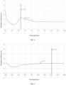
- FIG. 3 is a schematic diagram of the wavelength and the absorption coefficient of a polymeric membrane using a blue PET thin film material of specific scenario embodiment 1 of the present application.
- the abscissa is the numerical range of wavelengths in nm
- the ordinate is the absorption coefficient in %.
- 31 represents the absorption coefficient of the polymeric membrane using the blue PET thin film material in different wavelength ranges.
- 32 represents the absorption coefficient of the polymeric membrane using the transparent PET thin film material in different wavelength ranges. It may be seen that the energy absorption coefficient of the polymeric membrane, using the blue PET thin film material, at a wavelength of 355 nm of the ultraviolet light is 53%, as shown by 33 in FIG. 3 .
- the adhesive film is a silicone adhesive with the thickness of 5 ⁇ m, and the specific parameters of the adhesive film are that: the visible light transmittance is ⁇ 90%, the energy absorption coefficient of the adhesive film for the ultraviolet light with the wavelength being 355 nm is ⁇ 5%, and the peeling strength is 10-15 gf/cm at 25°C.
- the thin film mask is composed of a laminated layer of a polymeric membrane and an adhesive film.
- FIG. 4 is a schematic diagram of the wavelength and the absorption coefficient of the polymeric membrane using a yellow PET thin film material of specific scenario embodiment 2 of the present application.
- the abscissa is the numerical range of wavelengths in nm
- the ordinate is the absorption coefficient in %.
- 41 represents the absorption coefficient of the polymeric membrane using the yellow PET thin film material in different wavelength ranges. It can be seen that the energy absorption coefficient of the polymeric membrane, using a yellow PET thin film material, at the wavelength of 530 nm of the green light is 23%, as shown by 42 in FIG. 4 .
- the adhesive film is a silicone adhesive with the thickness of 7 ⁇ m, and the specific parameters of the adhesive film are that: the visible light transmittance is ⁇ 40%, the energy absorption coefficient of the adhesive film for the green light with the wavelength being 530 nm is ⁇ 35%, and the peeling strength is 20-25 gf/cm at 25°C.
- the thin film mask is composed of a laminated layer of a polymeric membrane and an adhesive film.
- the 15 ⁇ m green PO thin film material is used as the polymeric membrane, and the specific parameters of the polymeric membrane using the 15 ⁇ m green PET thin film material are that: the visible light transmittance is ⁇ 80%, and the energy absorption coefficient of the polymeric membrane for the infrared light with the wavelength being 1065 nm is ⁇ 20%.
- FIG. 5 is a schematic diagram of the wavelength and the absorption coefficient of a polymeric membrane using a green PO thin film material of specific scenario embodiment 3 of the present application. As shown in FIG. 5 , the abscissa is the numerical range of wavelengths in nm, and the ordinate is the absorption coefficient in %. In FIG.
- 51 represents the absorption coefficient of the polymeric membrane using the green PO film material in different wavelength ranges. It can be seen that the energy absorption coefficient of the polymeric membrane, using the green PO thin film material, at the wavelength of 1065 nm of the infrared light is 20% , as shown by 52 in FIG. 5 .
- the adhesive film is a silicone adhesive with the thickness of 10 ⁇ m, and the specific parameters of the adhesive film are that: the visible light transmittance is ⁇ 80%, the energy absorption coefficient of the adhesive film for the infrared light with the wavelength being 1065 nm is ⁇ 25%, and the peeling strength is 10-15 gf/cm at 20°C.
- the thin film mask is composed of a laminated layer of a polymeric membrane and an adhesive film.
- the 5 ⁇ m brown PI thin film material is used as the polymeric membrane, and the specific parameters of the polymeric membrane using the 5 ⁇ m brown PI thin film material are that: the visible light transmittance is ⁇ 80%, and the energy absorption coefficient of the polymeric membrane for the ultraviolet light with the wavelength being 355 nm is ⁇ 20%.
- the adhesive film is a silicone adhesive with the thickness of 5 ⁇ m, and the specific parameters of the adhesive film are that: the visible light transmittance is ⁇ 80%, the energy absorption coefficient of the adhesive film for the ultraviolet light with the wavelength being 355 nm is ⁇ 20%, and the peeling strength is 15-20 gf/cm at 20°C.
- the thin film mask is composed of a laminated layer of a polymeric membrane and an adhesive film.
- the 10 ⁇ m blue PVC thin film material is used as the polymeric membrane, and the specific parameters of the polymeric membrane using the 10 ⁇ m blue PVC thin film material are that: the visible light transmittance is ⁇ 70%, and the energy absorption coefficient of the polymeric membrane for the ultraviolet light with the wavelength being 343 nm is ⁇ 40%.
- the adhesive film is a acrylic adhesive with the thickness of 7 ⁇ m, and the specific parameters of the adhesive film are that: the visible light transmittance is ⁇ 80%, the energy absorption coefficient of the adhesive film for the ultraviolet light with the wavelength being 343 nm is ⁇ 30%, and the peeling strength is 20-25 gf/cm at 20°C.
- the thin film mask is composed of a laminated layer of a polymeric membrane and an adhesive film.
- the 20 ⁇ m brown BOPP thin film material is used as the polymeric membrane, and the specific parameters of the polymeric membrane using the 20 ⁇ m brown BOPP thin film material are that: the visible light transmittance is ⁇ 80%, and the energy absorption coefficient of the polymeric membrane for the infrared light with the wavelength being 1030 nm is ⁇ 15%.
- the adhesive film is a polyurethane adhesive with the thickness of 15 ⁇ m, and the specific parameters of the adhesive film are that: the visible light transmittance is ⁇ 90%, the energy absorption coefficient of the adhesive film for the infrared light with the wavelength being 1030 nm is ⁇ 20%, and the peeling strength is 25-30 gf/cm at 20°C.
- the thin film mask is composed of a laminated layer of a polymeric membrane and an adhesive film.
- the 5 ⁇ m blue PET thin film material is used as the polymeric membrane, and the specific parameters of the polymeric membrane using the 5 ⁇ m blue PET thin film material are that: the visible light transmittance is ⁇ 90%, and the energy absorption coefficient of the polymeric membrane for the ultraviolet light with the wavelength being 355 nm is ⁇ 20%.
- the adhesive film is a unidirectional thermo-sensitive adhesive with the thickness of 5 ⁇ m, and the specific parameters of the adhesive film are that: the visible light transmittance is ⁇ 73%, the energy absorption coefficient of the adhesive film for the ultraviolet light with the wavelength being 355 nm is ⁇ 10%, and the peeling strength is 20-25 gf/cm at 15-25°C; the peeling strength is 20-30 gf/cm at 50-100°C ; and the peeling strength is 5-7 gf/cm at 140°C.
- the thin film mask is composed of a laminated layer of a polymeric membrane and an adhesive film.
- the 8 ⁇ m red PO thin film material is used as the polymeric membrane, and the specific parameters of the polymeric membrane using the 8 ⁇ m red PO thin film material are that: the visible light transmittance is ⁇ 43%, and the energy absorption coefficient of the polymeric membrane for the green light with the wavelength being 545 nm is ⁇ 36%.
- the adhesive film is a unidirectional thermo-sensitive adhesive with the thickness of 7 ⁇ m, and the specific parameters of the adhesive film are that: the visible light transmittance is ⁇ 32%, the energy absorption coefficient of the adhesive film for the green light with the wavelength being 545 nm is ⁇ 41%, and the peeling strength is 23-25 gf/cm at 20-30°C; the peeling strength is 17-24 gf/cm at 60-110°C; and the peeling strength is 5-6 gf/cm at 130°C.
- the thin film mask is composed of a laminated layer of a polymeric membrane and an adhesive film.
- the 6 ⁇ m blue PET thin film material is used as the polymeric membrane, and the specific parameters of the polymeric membrane using the 6 ⁇ m blue PET thin film material are that: the visible light transmittance is ⁇ 80%, and the energy absorption coefficient of the polymeric membrane for the ultraviolet light with the wavelength being 350 nm is ⁇ 25%.
- the adhesive film is a bidirectional thermo-sensitive adhesive with the thickness of 6 ⁇ m, and the specific parameters of the adhesive film are that: the visible light transmittance is ⁇ 61%, the energy absorption coefficient of the adhesive film for the ultraviolet light with the wavelength being 350 nm is ⁇ 5%, and the peeling strength is 5-7 gf/cm at 50°C; the peeling strength is 15-21 gf/cm at 80-100°C ; and the peeling strength is 26-30 gf/cm at 120-140°C.
- the thin film mask is composed of a laminated layer of a polymeric membrane and an adhesive film.
- the 10 ⁇ m red BOPP thin film material is used as the polymeric membrane, and the specific parameters of the polymeric membrane using the 10 ⁇ m red BOPP thin film material are that: the visible light transmittance is ⁇ 75%, and the energy absorption coefficient of the polymeric membrane for the green light with the wavelength being 520 nm is ⁇ 45%.
- the adhesive film is a bidirectional thermo-sensitive adhesive with the thickness of 8 ⁇ m, and the specific parameters of the adhesive film are that: the visible light transmittance is ⁇ 49%, the energy absorption coefficient of the adhesive film for the green light with the wavelength being 520 nm is ⁇ 12%, and the peeling strength is 6-10 gf/cm at 55°C; the peeling strength is 12-19 gf/cm at 70-90°C; and the peeling strength is 20-25 gf/cm at 100-130°C.
- the thin film mask is composed of a laminated layer of a polymeric membrane, an adhesive film and a release film.
- the 8 ⁇ m blue PVC thin film material is used as the polymeric membrane, and the specific parameters of the polymeric membrane using the 8 ⁇ m blue PVC thin film material are that: the visible light transmittance is ⁇ 80%, and the energy absorption coefficient of the polymeric membrane for the ultraviolet light with the wavelength being 340 nm is ⁇ 30%.
- the adhesive film is a silicone adhesive with the thickness of 9 ⁇ m, and the specific parameters of the adhesive film are that: the visible light transmittance is ⁇ 8%, the energy absorption coefficient of the adhesive film for the ultraviolet light with the wavelength being 340 nm is ⁇ 34%, and the peeling strength is 16-18 gf/cm at 25°C.
- the release film is a transparent PET film with the thickness of 5 ⁇ m.
- the thin film mask is composed of a laminated layer of a polymeric membrane, an adhesive film and a release film.
- the 10 ⁇ m green PO thin film material is used as the polymeric membrane, and the specific parameters of the polymeric membrane using the 10 ⁇ m green PO thin film material are that: the visible light transmittance is ⁇ 48%, and the energy absorption coefficient of the polymeric membrane for the infrared light with the wavelength being 1065 nm is ⁇ 39%.
- the adhesive film is a silicone adhesive with the thickness of 8 ⁇ m, and the specific parameters of the adhesive film are that: the visible light transmittance is ⁇ 31%, the energy absorption coefficient of the adhesive film for the infrared light with the wavelength being 1065 nm is ⁇ 31%, and the peeling strength is 10-15 gf/cm at 25°C.
- the release film is a transparent PET film with the thickness of 5 ⁇ m.
- the thin film mask are shown below, and are applied in the field of manufacturing the solar cell piece, and are specifically applied in the process of manufacturing an electrode gate line.
- the features of the thin film mask specifically used are that: the thin film mask is composed of a laminated layer of a polymeric membrane and an adhesive film; the 5 ⁇ m blue PET thin film is used as the polymeric membrane, the visible light transmittance of the polymeric membrane is ⁇ 73%, and the energy absorption coefficient of the polymeric membrane for the ultraviolet light with the wavelength being 350 nm is ⁇ 47%.
- the adhesive film is a silicone adhesive with the thickness of 5 ⁇ m, the visible light transmittance of the silicone adhesive is ⁇ 54%, the energy absorption coefficient of the adhesive film for the ultraviolet light with the wavelength being 350 nm is ⁇ 24%, and the peeling strength of the adhesive film is 10-15 gf/cm at 25 °C.
- the energy absorptions of the polymeric membrane and the adhesive film are better in the wavelength range of the ultraviolet light.
- an ultraviolet laser is used to carve a thin film mask to form a patterned content, the power requirement of the ultraviolet laser is small, and costs may be saved.
- the peeling strength range of the adhesive film an appropriate numerical range is adopted, so that the adhesion of the thin film mask meets the processing requirements, the thin film mask cannot be too loose or too sticky. That is to say, the thin film mask can not fall off during the process of manufacturing the electrode gate lines, and the solar cell piece may also not be damaged during the process of tearing off the film after the electrode gate lines are manufactured.
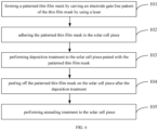
- FIG. 6 is a schematic diagram of a method for manufacturing an electrode gate line for a solar cell piece of specific application embodiment 1 of the present application.
- the specific method in the present embodiment includes the steps as follows: S101, forming a patterned thin film mask by carving an electrode gate line pattern of the thin film mask by using a laser.
- a designed pattern is carved on a thin film mask by using the laser etching process.
- a picosecond ultraviolet light source with a wavelength of 350 nm is used by the laser.
- the width of the pattern is 1 ⁇ m-500 ⁇ m; further optionally, the width of the pattern is 1 ⁇ m-20 ⁇ m.
- the spacing of the pattern line is 50 ⁇ m-5 mm; further optionally, the spacing of the pattern line is 500 ⁇ m-2 mm.
- the pattern designed on the thin film mask is an electrode gate line pattern on a subsequent solar cell piece.
- the selection of the width of the pattern and the line spacing of the pattern may be adjusted accordingly depending on the use scenario and requirements.
- the thin film mask with the carved electrode gate line pattern is adhered to a surface of the solar cell piece on which the electrode gate line needs to be disposed, i.e., a surface of the silicone adhesive of the thin film mask exposed to the outside is adhered to the solar cell piece.
- the solar cell piece pasted with the patterned thin film mask is subjected to the deposition treatment.
- the metal electrode gate lines are manufactured by using the method of the physical vapor deposition (PVD), or the electrode gate lines are manufactured on the solar cell piece by using the method of electroplating.
- PVD physical vapor deposition
- electroplating the method of electroplating
- the patterned thin film mask on the solar cell piece after the deposition treatment is peeled off.
- the electrode gate lines are not formed in the covered regions on the solar cell piece, and the electrode gate lines are formed on the uncovered regions on the solar cell piece.
- the solar cell piece forming the patterned electrode gate lines is annealed to complete the manufacturing of the electrode gate lines.
- the features of the thin film mask specifically used are that: the thin film mask is composed of a laminated layer of a polymeric membrane, an adhesive film and a release film; the 10 ⁇ m red BOPP thin film is used as the polymeric membrane, the visible light transmittance of the polymeric membrane is ⁇ 48% and an energy absorption coefficient of the polymeric membrane for the green light with the wavelength being 530nm is ⁇ 31%.
- the adhesive film is a silicone adhesive with the thickness of 3 ⁇ m, the visible light transmittance of the adhesive film is ⁇ 61%, the energy absorption coefficient of the adhesive film for the green light with the wavelength being 530nm is ⁇ 32%, and the peeling strength of the adhesive film is 16-21 gf/cm at 20°C.
- the release film is a transparent PET film with the thickness of 10 ⁇ m.
- the energy absorptions of the polymeric membrane and the adhesive film are better in the wavelength range of the green light.
- the power requirement of the green laser is small, and costs may be saved.
- the peeling strength range of the adhesive film an appropriate numerical range is adopted, so that the adhesion of the thin film mask meets the processing requirements, the thin film mask cannot be too loose or too sticky. That is to say, the thin film mask can not fall off during the process of manufacturing the electrode gate lines, and the solar cell piece may also not be damaged during the process of tearing off the film after the electrode gate lines are manufactured.
- FIG. 7 is a schematic diagram of a method for manufacturing an electrode gate line for a solar cell piece of specific application embodiment 2 of the present application. As shown in FIG. 7 , the specific method in the present embodiment includes the steps as follows:
- a designed pattern is carved on a thin film mask by using the laser etching process.
- a picosecond green light source with a wavelength of 530 nm is used by the laser.
- the width of the pattern is 1 ⁇ m-500 ⁇ m; further optionally, the width of the pattern is 1 ⁇ m-20 ⁇ m.
- the spacing of the pattern line is 50 ⁇ m-5 mm; further optionally, the spacing of the pattern line is 500 ⁇ m-2 mm.
- the pattern designed on the thin film mask is an electrode gate line pattern on a subsequent solar cell piece.
- the selection of the width of the pattern and the line spacing of the pattern may be adjusted accordingly depending on the use scenario and requirements.
- the thin film mask is adhered to a surface of the solar cell piece on which the electrode gate line needs to be disposed, i.e., a surface of the silicone adhesive of the thin film mask exposed to the outside is adhered to the solar cell piece.
- the solar cell piece pasted with the patterned thin film mask is subjected to the deposition treatment.
- the metal electrode gate lines are manufactured by using the method of the physical vapor deposition (PVD), or the electrode gate lines are manufactured on the solar cell pieces by using the method of electroplating.
- PVD physical vapor deposition
- electroplating the method of electroplating
- the patterned thin film mask on the solar cell piece after the deposition treatment is peeled off.
- the electrode gate lines are not formed in the covered regions on the solar cell piece, and the electrode gate lines are formed in the uncovered regions on the solar cell piece.
- the solar cell piece forming the patterned electrode gate lines is annealed to complete the manufacturing of the electrode gate lines.
- the features of the thin film mask specifically used are that: the thin film mask is composed of a laminate layer of a polymeric membrane and an adhesive film; the 15 ⁇ m blue PO thin film material is used as the polymeric membrane, the visible light transmittance of the polymeric membrane is ⁇ 62%, and the energy absorption coefficient of the polymeric membrane for the ultraviolet light with the wavelength being 355 nm is ⁇ 58%.
- the adhesive film is a unidirectional thermo-sensitive adhesive with the thickness of 10 ⁇ m, the visible light transmittance of the adhesive film is ⁇ 75%, and the energy absorption coefficient of the adhesive film for the ultraviolet light with the wavelength being 355 nm is ⁇ 24%, and the peeling strength of the adhesive film is 35 gf/cm at 20°C; the peeling strength of the adhesive film is 20-30 gf/cm at 50-85 °C ; and the peeling strength of the adhesive film is 5 gf/cm at 140°C .
- the energy absorptions of the polymeric membrane and the adhesive film are better in the wavelength range of the ultraviolet light.
- a ultraviolet laser is used to carve a thin film mask to form a patterned content, the power requirement of the ultraviolet laser is small, and costs may be saved.
- the peeling strength range of the adhesive film an appropriate numerical range is adopted, so that the adhesion of the thin film mask meets the processing requirements, the thin film mask cannot be too loose or too sticky. That is to say, the thin film mask can not fall off during the process of manufacturing the electrode gate lines, and the solar cell piece may also not be damaged during the process of tearing off the film after the electrode gate lines are manufactured.
- FIG. 8 is a schematic diagram of a method for manufacturing an electrode gate line for a solar cell piece of specific application embodiment 3 of the present application.
- the specific method in the present embodiment includes the steps as follows: Firstly, a designed pattern is carved on a thin film mask by using the laser etching process. A picosecond ultraviolet light source with a wavelength of 350 nm is used by the laser.
- the width of the pattern is 1 ⁇ m-500 ⁇ m; further optionally, the width of the pattern is 1 ⁇ m-20 ⁇ m.
- the spacing of the pattern line is 50 ⁇ m-5 mm, further optionally, the spacing of the pattern line is 500 ⁇ m-2 mm.
- the pattern designed on the thin film mask is an electrode gate line pattern on a subsequent solar cell piece.
- the selection of the width of the pattern and the line spacing of the pattern may be adjusted accordingly depending on the use scenario and requirements.
- the thin film mask with the carved electrode gate line pattern is adhered to a surface of the solar cell piece on which the electrode gate line needs to be disposed, i.e., a surface of the unidirectional thermo-sensitive adhesive of the thin film mask exposed to the outside is adhered to the solar cell piece.
- the solar cell piece pasted with the patterned thin film mask is subjected to the deposition treatment.
- the metal electrode gate lines are manufactured by using the method of the physical vapor deposition (PVD), or the electrode gate lines are manufactured on the solar cell pieces by using the method of electroplating.
- PVD physical vapor deposition
- electroplating the method of electroplating
- the heating is performed by using the hot filament at 150°C for 5 minutes, or by using the infrared lamp at 150 °C for 10 minutes. Since the peeling strength of the unidirectional thermo-sensitive adhesive at 150 °C is weakened comparing with the peeling strength at a room temperature, it is relatively easy to peel off the patterned thin film mask on the solar cell piece after the deposition treatment. Finally, the electrode gate lines are not formed on the covered regions on the solar cell piece, and the electrode gate lines are formed on the uncovered regions on the solar cell piece.
- the solar cell piece forming the patterned electrode gate lines is annealed to complete the manufacturing of the electrode gate lines.
- the features of the thin film mask specifically used are that: the thin film mask is composed of a laminated layer of a polymeric membrane and an adhesive film laminate; the 20 ⁇ m green PVC thin film is used as the polymeric membrane, the visible light transmittance of the polymeric membrane is ⁇ 58%, and the energy absorption coefficient of the polymeric membrane for the green light with the wavelength being 547 nm is ⁇ 39%.
- the adhesive film is a bidirectional thermo-sensitive adhesive with the thickness of 15 ⁇ m, the visible light transmittance of the adhesive film is ⁇ 41%, the energy absorption coefficient of the adhesive film for the green light with the wavelength being 547 nm is ⁇ 65%, and the peeling strength of the adhesive film is 5 gf/cm at 25°C; the peeling strength of the adhesive film is 17-22 gf/cm at 50-80°C and the peeling strength of the adhesive film is 27-30 gf/cm at 120-140°C.
- the energy absorptions of the polymeric membrane and the adhesive film are better in the wavelength range of the green light.
- the power requirement of the green laser is small, and costs may be saved.
- the peeling strength range of the adhesive film an appropriate numerical range is adopted, so that the adhesion of the thin film mask meets the processing requirements, the thin film mask cannot be too loose or too sticky. That is to say, the thin film mask can not fall off during the process of manufacturing the electrode gate lines, and the solar cell piece may also not be damaged during the process of tearing off the film after the electrode gate lines are manufactured.
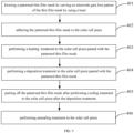
- FIG. 9 is a schematic diagram of a method for manufacturing an electrode gate line for a solar cell piece of specific application embodiment 4 of the present application.
- the specific method in the present embodiment includes the steps as follows: S401, forming a patterned thin film mask by carving an electrode gate line pattern of the thin film mask by using a laser.
- a designed pattern is carved on a thin film mask by usig the laser etching process.
- a picosecond ultraviolet light source with a wavelength of 547 nm is used by the laser.
- the width of the pattern is 1 ⁇ m-500 ⁇ m; further optionally, the width of the pattern is 1 ⁇ m-20 ⁇ m.
- the spacing of the pattern line is 50 ⁇ m-5 mm, further optionally, the spacing of the pattern line is 500 ⁇ m-2 mm.
- the pattern designed on the thin film mask is an electrode gate line pattern on a subsequent solar cell piece.
- the selection of the width of the pattern and the line spacing of the pattern may be adjusted accordingly depending on the use scenario and requirements.
- the thin film mask with the carved electrode gate line pattern is adhered to a surface of the solar cell piece on which the electrode gate line needs to be disposed, i.e., a surface of the bidirectional thermo-sensitive adhesive of the thin film mask exposed to the outside is adhered to the solar cell piece.
- the solar cell piece pasted with the patterned thin film mask is heated by means of heating, the peeling strength of the bidirectional thermo-sensitive adhesive increases with the increasing of the temperature, so that the patterned thin film mask and the solar cell piece are adhered more firmly by means of heating, so as to facilitate the processing and treatment of subsequent processes.
- the method of heating is achieved by means of, for example, heating at 130°C for 2 minutes by using a hot filament, or heating at 70 °C for 5 minutes by using an infrared lamp, etc.
- the solar cell piece pasted with the patterned thin film mask is subjected to the deposition treatment.
- the metal electrode gate lines are manufactured by using the method of the physical vapor deposition (PVD), or the electrode gate lines are manufactured on the solar cell pieces by using the method of electroplating.
- PVD physical vapor deposition
- electroplating the method of electroplating
- the bidirectional thermo-sensitive adhesive has reversibility, namely, the peeling strength increases with the increasing of a temperature, and the peeling strength decreases with the decreasing of a temperature.
- the temperature of the solar cell piece after the deposition treatment namely, after the cooling treatment
- the electrode gate lines are not formed in the covered regions on the solar cell piece, and the electrode gate lines are formed in the uncovered regions on the solar cell piece.
- the solar cell piece forming the patterned electrode gate lines is annealed to complete the manufacturing of the electrode gate lines.
Landscapes
- Chemical & Material Sciences (AREA)
- Chemical Kinetics & Catalysis (AREA)
- Engineering & Computer Science (AREA)
- Materials Engineering (AREA)
- Mechanical Engineering (AREA)
- Metallurgy (AREA)
- Organic Chemistry (AREA)
- Laminated Bodies (AREA)
- Physical Vapour Deposition (AREA)
- Preparing Plates And Mask In Photomechanical Process (AREA)
Abstract
Description
- The present disclosure claims the priority of the Chinese patent application filed on
September 10th, 2021 before the Chinese Patent Office with the application number of 202111063887.5 - The present application relates to the technical field of thin film materials and, more particular, to a thin film mask.
- The method of using a thin film mask to make regional patterns is widely used in high-tech fields such as semiconductors, display panels, touch panels, solar cells, circuit masks and precision printing. At present, a commonly used method is to use photoresist development or pattern a metal mask. The photoresist process is complicated, the material cost is high, the subsequent chemical cleaning is required, the cost of environmental requirements is increased. However, when the metal mask is especially applied to a solar cell with concave and convex surfaces, the metal mask cannot be fit to the surface of the solar cell, which results in low accuracy of the patterned content. In addition, periodic maintenance and cleaning are required during use and the maintenance cost is increased.
- An object of the present application aims at providing a thin film mask, wherein the thin film mask includes a first layer and a second layer; the first layer and the second layer are arranged in layer configuration; and the second layer includes an adhesive film;
- under irradiation of an ultraviolet light source and with a thickness of the first layer being 200 µm or less, an absorption coefficient of the first layer is ≥ 20%, wherein a wavelength of the ultraviolet light source is 355 ± 15 nm; or under irradiation of a green light source and with the thickness of the first layer being 200 µm or less, the absorption coefficient of the first layer is ≥ 20%, wherein a wavelength of the green light source is 530 ± 15 nm; or under irradiation of an infrared light source and with the thickness of the first layer being 200 µm or less, the absorption coefficient of the first layer is ≥ 20%, wherein a wavelength of the infrared light source is 1045 ± 20 nm; and
- a visible light transmittance of the first layer is ≤ 90%.
- Further, under the irradiation of the ultraviolet light source and with the thickness of the first layer being 200 µm or less, the absorption coefficient of the first layer is ≥ 50%; optionally, under the irradiation of the ultraviolet light source and with the thickness of the first layer being 200 µm or less, the absorption coefficient of the first layer is ≥ 80%; or
- under the irradiation of the green light source and with the thickness of the first layer being 200 µm or less, the absorption coefficient of the first layer is ≥ 50%; optionally, under the irradiation of the green light source and with the thickness of the first layer being 200 µm or less, the absorption coefficient of the first layer is ≥ 80%; or
- under the irradiation of the infrared light source and with the thickness of the first layer being 200 µm or less, the absorption coefficient of the first layer is ≥ 50%; and optionally, under the irradiation of the infrared light source and with the thickness of the first layer being 200 µm or less, the absorption coefficient of the first layer is ≥ 80%.
- Further, the first layer includes a polymeric membrane;
a material of the polymeric membrane is a polymer, including one or more of polyethylene glycol terephthalate (PET), polyolefin thin film (PO), polyimide (PI), polyvinyl chloride (PVC), and biaxially oriented polypropylene (BOPP). - Further, the thickness of the first layer is 1-100 µm; optionally, the thickness of the first layer is 5-40 µm; and further optionally, the thickness of the first layer is 10-25 µm.
- Further, under the irradiation of the ultraviolet light source and with a thickness of the second layer being 200 µm or less, an absorption coefficient of the second layer is ≥ 5%, wherein the wavelength of the ultraviolet light source is 355 ± 15nm; or under the irradiation of the green light source and with the thickness of the second layer being 200 µm or less, the absorption coefficient of the second layer is ≥ 5%, wherein the wavelength of the green light source is 530 ± 15nm; or, under the irradiation of the infrared light source and with the thickness of the second layer being 200 µm or less, the absorption coefficient of the second layer is ≥ 5%, wherein the wavelength of the infrared light source is 1045 ± 20 nm.
- Further, under the irradiation of the ultraviolet light source and with a thickness of the second layer being 200 µm or less, an absorption coefficient of the second layer is ≥ 50%; optionally, under the irradiation of the ultraviolet light source and with the thickness of the second layer being 200 µm or less, the absorption coefficient of the second layer is ≥ 80%; or
- under the irradiation of the green light source and with the thickness of the second layer being 200 µm or less, the absorption coefficient of the second layer is ≥ 50%; optionally, under the irradiation of the green light source and with the thickness of the second layer being 200 µm or less, the absorption coefficient of the second layer is ≥ 80%; or
- under the irradiation of the infrared light source and with the thickness of the second layer being 200 µm or less, the absorption coefficient of the second layer is ≥ 50%; and optionally, under the irradiation of the infrared light source and with the thickness of the second layer being 200 µm or less, the absorption coefficient of the second layer is ≥ 80%.
- Further, a thickness of the second layer is 1-30 µm; optionally, the thickness of the second layer is 2-15 µm; and further optionally, the thickness of the second layer is 3-10 µm.
- Further, a material of the adhesive film in the second layer includes one or more of silicone, acrylic adhesive, polyurethane, rubber, and polyisobutylene.
- Further, a peeling strength of the second layer at a first temperature is 1-50 gf/cm; optionally, the peeling strength of the second layer is 5-30 gf/cm; and further optionally, the peeling strength of the second layer is 6-15 gf/cm;
wherein the first temperature is 15-30°C; optionally, the first temperature is 20-30°C; further optionally, the first temperature is 20-25 °C. - Further, a material of the adhesive film in the second layer includes a unidirectional thermo-sensitive adhesive, a viscosity of the unidirectional thermo-sensitive adhesive exhibits irreversibility under different temperature conditions; and
a peeling strength of the unidirectional thermo-sensitive adhesive decreases with increasing of a temperature. - Further, a material of the adhesive film in the second layer includes a thermal debonding adhesive, a viscidity of the thermal debonding adhesive exhibits irreversibility at a temperature greater than or equal to a second temperature; and
- a peeling strength of the thermal debonding adhesive at the temperature greater than or equal to the second temperature is less than a peeling strength of the thermal debonding adhesive at a temperature less than the second temperature;
- wherein the second temperature is 70 °C; optionally, the second temperature is 70-150°C; and further optionally, the second temperature is 90-150°C.
- Further, the peeling strength of the unidirectional thermo-sensitive adhesive is 5-30 gf/cm and the temperature is 50-140°C.
- Further, a material of the adhesive film in the second layer includes a bidirectional thermo-sensitive adhesive, a viscosity of the bidirectional thermo-sensitive adhesive exhibits reversibility under different temperature conditions; and
a peeling strength of the bidirectional thermo-sensitive adhesive increases with increasing of a temperature. - Further, the peeling strength of the bidirectional thermo-sensitive adhesive is 5-30 gf/cm and the temperature is 50-140°C.
- Further, a thickness of the thin film mask is 10-100 µm; optionally, the thickness of the thin film mask is 10-50 µm.
- Further, the thin film mask further includes a third layer;
- the third layer is arranged in layer configuration at a side of the second layer away from the first layer;
- the third layer includes a release film; and
- the release film is a polymer, including one or more of polyethylene glycol terephthalate (PET), polyolefin thin film (PO), polyimide (PI), polyvinyl chloride (PVC), and biaxially oriented polypropylene (BOPP).
- Further, a thickness of the third layer is 1-100 µm; optionally, the thickness of the third layer is 5-40 µm; and further optionally, the thickness of the third layer is 10-25 µm.
- Another object of the present application aims at providing a deposition process for a solar cell, wherein the thin film mask stated above is used in the deposition process.
- Further, the deposition process includes a functional layer deposition process and/or a conductive layer deposition process;
wherein the functional layer deposition includes a dielectric layer deposition; and the conductive layer deposition includes a transparent conductive layer deposition and/or a metal conductive layer deposition. - In conclusion, a thin film mask is provided by the present application, by setting specific optical properties, such as the limitation of the absorption coefficient and the visible light transmittance, for the first layer, a patterning treatment is performed on the first layer by being irradiated by some light sources with specific wavelength ranges, such as the ultraviolet laser, the green laser or the infrared laser. Then, by utilizing that an adhesive film of a second layer has an adhesive characteristic, the patterned thin film mask is adhered to a target object to be treated, and subsequent region pattern manufacturing is performed. The solution of the present application has the following characteristics:
- In comparison to the photoresist development, the optical properties are utilized by the thin film mask provided by the present application, the required power of the light source is less and cost can be saved comparing with a common thin film. Furthermore, the patterning content is formed by a light source with low power consumption, and the cost of the adhesive film is low. A complicated process is not needed to be matched with to achieve the patterning process, and cost reduction and efficiency increase are achieved. In addition, comparing with a metal mask, the thin film mask provided by the present application is adhered to the surface of the target object to be treated via the adhesive film, so that the thin film mask is better bonded to the surface. Comparing with the method of the metal mask, the thin film mask is not affected by the hollow region, so that the patterned content is more accurate and the quality is improved.
- The above description is only an overview of the technical solution of the present disclosure, in order to be able to better understand the technical means of the present disclosure, and the solution can be implemented in accordance with the content of the description, and in order to make the above and other purposes, features and advantages of the present disclosure more obvious and easy to understand, the following specific embodiments of the present disclosure are hereby given.
- In order to explain embodiments of the present disclosure or the technical scheme in the prior art more clearly, the drawings required in the description of the embodiments or the prior art will be briefly introduced below; obviously, the drawings in the following description are some embodiments of the present disclosure, and other drawings can be obtained according to these drawings by those of ordinary skill in the art without paying creative labor.
-
FIG. 1 is a schematic diagram of a structure of a thin film mask ofembodiment 1 of the present application; -
FIG. 2 is a schematic diagram of a structure of a thin film mask ofembodiment 2 of the present application; -
FIG. 3 is a schematic diagram of the wavelength and the absorption coefficient of a polymeric membrane using a blue PET thin film material ofspecific scenario embodiment 1 of the present application; -
FIG. 4 is a schematic diagram of the wavelength and the absorption coefficient of a polymeric membrane using a yellow PET thin film material ofspecific scenario embodiment 2 of the present application; -
FIG. 5 is a schematic diagram of the wavelength and the absorption coefficient of a polymeric membrane using a green PO thin film material ofspecific scenario embodiment 3 of the present application; -
FIG. 6 is a schematic diagram of a method for manufacturing an electrode gate line for a solar cell piece ofspecific application embodiment 1 of the present application; -
FIG. 7 is a schematic diagram of a method for manufacturing an electrode gate line for a solar cell piece ofspecific application embodiment 2 of the present application; -
FIG. 8 is a schematic diagram of a method for manufacturing an electrode gate line for a solar cell piece ofspecific application embodiment 3 of the present application; and -
FIG. 9 is a schematic diagram of a method for manufacturing an electrode gate line for a solar cell piece of specific application embodiment 4 of the present application. - In order to make the purpose, technical solution and advantages of embodiments of the present disclosure clearer, the following will be combined with the accompanying drawings in the embodiments of the present disclosure, the technical solutions in the embodiments of the present disclosure are clearly and completely described, obviously, the described embodiments are a part of the embodiments of the present disclosure, not all embodiments. Based on the embodiments in the present disclosure, all other embodiments obtained by those of ordinary skill in the art without paying creative labor are within the scope of protection of the present disclosure.
- In order to make the technical problems, technical solutions and beneficial effects to be solved in the present application more clear, the following combined with the drawings and embodiments, the present application is further explained in detail. It should be understood that the specific embodiments described herein are merely used for explaning the present application and are not used to limit the present application.
- The terms "first", "second", "third", "fourth", and the like (if any) in the speicifcation and claims and the above-described figures of the present application, are used for distinguishing between similar objects and not necessarily used for decarving a particular sequence or chronological order. It should be understood that the data used in this way may be interchanged, where appropriate, so that the embodiments of the present application described herein can be implemented in an order other than those illustrated or described herein. Furthermore, the terms "including" and "having", as well as any variations thereof, are intended to cover a non-exclusive inclusion. For example, a process, a method, a system, a product, or a device that includes a list of steps or units is not necessarily limited to those steps or units expressly listed, but may include other steps or units not expressly listed or inherent to these processes, methods, articles, or devices.
- The technical solutions of the present disclosure will be described in detail in combination with specific embodiments below. The following specific embodiments may be combined with one another, and the same or similar concepts or processes may not be repeated in some embodiments.
-
Embodiment 1, a thin film mask with a two-layer laminated structure - A structure of a thin film mask with a two-layer laminated structure is provided by the embodiment of the present application.
FIG. 1 is a schematic diagram of a structure of a thin film mask ofembodiment 1 of the present application. As shown inFIG. 1 , the structure of the thin film mask includes: - a
first layer 1 and asecond layer 2, thefirst layer 1 and thesecond layer 2 are arranged in layer configuration; and thesecond layer 2 includes an adhesive film; - under irradiation of an ultraviolet light source and with a thickness of the first layer being 200 µm or less, an absorption coefficient of the
first layer 1 is ≥ 20%, wherein a wavelength of the ultraviolet light source is 355 ± 15 nm. - Alternatively, under irradiation of a green light source and with the thickness of the first layer being 200 µm or less, the absorption coefficient of the
first layer 1 is ≥ 20%, wherein a wavelength of the green light source is 530 ± 15 nm. - Alternatively, under irradiation of an infrared light source and with the thickness of the first layer being 200 µm or less, the absorption coefficient of the
first layer 1 is ≥ 20%, wherein a wavelength of the infrared light source is 1045 ± 20 nm. - A visible light transmittance of the
first layer 1 is ≤ 90%. - A thin film mask is provided in the present embodiment, by setting specific optical properties, such as the limitation of the absorption coefficient and the visible light transmittance, for the first layer, a patterning treatment is performed on the first layer by being irradiated by some light sources with specific wavelength ranges, such as the ultraviolet laser, the green laser or the infrared laser. Then, by utilizing that an adhesive film of a second layer has an adhesive characteristic, the patterned thin film mask is adhered to a target object to be treated, and subsequent region pattern manufacturing is performed.
- In comparison to the photoresist development, optical properties are utilized by the thin film mask provided by the present application, the required power of the light source is less and cost can be saved comparing with a common thin film. Furthermore, the patterning content is formed by a light source with low power consumption, and the cost of the adhesive film is low. A complicated process is not needed to be matched with to achieve the patterning process, and cost reduction and efficiency increase are achieved. In addition, comparing with a metal mask, the thin film mask provided by the present application is adhered to the surface of the target object to be treated via the adhesive film, so that the thin film mask is better bonded to the surface. Comparing with the method of the metal mask, the thin film mask is not affected by the hollow region, so that the patterned content is more accurate and the quality is improved.
- A structure of a thin film mask of a three-layer laminated structure is provided by the embodiment of the present application.
FIG. 2 is a schematic diagram of a structure of a thin film mask ofembodiment 2 of the present application. As shown inFIG. 2 , the structure of the thin film mask includes: - a
first layer 1, asecond layer 2 and athird layer 3, wherein thefirst layer 1, thesecond layer 2 and thethird layer 3 are arranged in layer configuration in sequence; thethird layer 3 is arranged in layer configuration at a side of thesecond layer 2 away from thefirst layer 1; and - the
second layer 2 includes an adhesive film and thethird layer 3 includes a release film. - Under irradiation of an ultraviolet light source and with a thickness of the first layer being 200 µm or less, an absorption coefficient of the
first layer 1 is ≥ 20%, wherein a wavelength of the ultraviolet light source is 355 ± 15 nm. - Alternatively, under irradiation of a green light source and with the thickness of the first layer being 200 µm or less, the absorption coefficient of the
first layer 1 is ≥ 20%, wherein a wavelength of the green light source is 530 ± 15 nm. - Alternatively, under irradiation of an infrared light source and with the thickness of the first layer being 200 µm or less, the absorption coefficient of the
first layer 1 is ≥ 20%, wherein a wavelength of the infrared light source is 1045 ± 20 nm. - A visible light transmittance of the
first layer 1 is ≤ 90%. - The thin film mask provided in the present embodiments, on the basis of the above-mentioned embodiment, further includes a release film, the function of the release film is to, during the patterning machining process of the thin film mask, protect the adhesive film from sticking other stuff during the machining and use, so as to facilitate tearing off the release film after the patterning machining process is completed and sticking the patterned film mask to a target object to be treated.
- Some of the features mentioned in the above embodiments are described in further detail below.
- Further, under the irradiation of the ultraviolet light source and with the thickness of the first layer being 200 µm or less, the absorption coefficient of the first layer is ≥ 50%; optionally, under the irradiation of the ultraviolet light source and with the thickness of the first layer being 200 µm or less, the absorption coefficient of the first layer is ≥ 80%.
- Alternatively, under the irradiation of the green light source and with the thickness of the first layer being 200 µm or less, the absorption coefficient of the first layer is ≥ 50%; optionally, under the irradiation of the green light source and with the thickness of the first layer being 200 µm or less, the absorption coefficient of the first layer is ≥ 80%.
- Alternatively, under the irradiation of the infrared light source and with the thickness of the first layer being 200 µm or less, the absorption coefficient of the first layer is ≥ 50%; and optionally, under the irradiation of the infrared light source and with the thickness of the first layer being 200 µm or less, the absorption coefficient of the first layer is ≥ 80%.
- In conjunction with the above description, for example, for the ultraviolet light source, the absorption coefficient of the first layer may be 20%, 25%, 30%, 35%, 40%, 45%, 50%, 55%, 60%, 65%, 70%, 75%, 80%, or any range therebetween, with the thickness of the first layer being 200 µm or less.
- In conjunction with the above description, for example, for the green light source, the absorption coefficient of the first layer may be 20%, 25%, 30%, 35%, 40%, 45%, 50%, 55%, 60%, 65%, 70%, 75%, 80%, or any range therebetween, with the thickness of the first layer being 200 µm or less.
- In conjunction with the above description, for example, for the infrared light source, the absorption coefficient of the first layer is 20%, 25%, 30%, 35%, 40%, 45%, 50%, 55%, 60%, 65%, 70%, 75%, 80%, or any range therebetween, with the thickness of the first layer being 200 µm or less.
- Further, the first layer includes a polymeric membrane. The material of the polymeric membrane is a polymer, including one or more of polyethylene glycol terephthalate (PET), polyolefin thin film (PO), polyimide (PI), polyvinyl chloride (PVC), biaxially oriented polypropylene (BOPP), and the like.
- In conjunction with the above description, for example, for the visible light transmittance of the first layer is ≤ 90%, the visible light transmittance may be 0%, 5%, 10%, 15%, 20%, 25%, 30%, 35%, 40%, 45%, 50%, 55%, 60%, 65%, 70%, 75%, 80%, 85%, 90%, or any range therebetween.
- Further, the thickness of the first layer is 1-100 µm; optionally, the thickness of the first layer is 5-40 µm; and further optionally, a visible light transmittance of the first layer is 10-25 µm.
- In connection with the above description, for example, the thickness of the first layer is 1 µm, 5 µm, 10 µm, 15 µm, 20 µm, 25 µm, 30 µm, 35 µm, 40 µm, 45 µm, 50 µm, 55 µm, 60 µm, 65 µm, 70 µm, 75 µm, 80 µm, 85 µm, 90 µm, 95 µm, 100 µm or any range therebetween.
- It should be noted here that the feature setting of the absorption coefficient of the first layer with respect to the above-mentioned various light sources may generally be achieved by adjusting the color of the first layer, adding an additive having an absorption characteristic, etc. For example, various dyes, additives, color masterbatches, or other materials are included in the PET film to meet the requirements for the absorption coefficient. For example, black particles are added in a BOPP film, an absorption coefficient of 100% is achieved, and as another example, grey particles are added in a PO film, an absorption coefficient of 50% is achieved.
- Further, under the irradiation of the ultraviolet light source and with the thickness of the second layer being 200 µm or less, an absorption coefficient of the adhesive film included by the second layer is ≥ 5%, wherein the wavelength of the ultraviolet light source is 355 ± 15nm. Alternatively, under the irradiation of the green light source and with the thickness of the second layer being 200 µm or less, the absorption coefficient of the second layer is ≥ 5%, wherein the wavelength of the green light source is 530 ± 15 nm. Alternatively, under the irradiation of the infrared light source and with the thickness of the second layer being 200 µm or less, the absorption coefficient of the second layer is ≥ 5%, wherein the wavelength of the infrared light source is 1045 ± 20 nm.
- In conjunction with the description above, the wavelength of the ultraviolet light source is 340 nm, 345 nm, 350 nm, 355 nm, 360 nm, 365 nm, 370 nm, or any range therebetween. For example, a laser light source, such as an ultrafast pulsed laser with a pulse width in the order of picoseconds or femtoseconds, or a short pulsed laser with a pulse width in the order of microseconds or nanoseconds, may be used as the ultraviolet light source here.
- In conjunction with the description above, the wavelength of the green light source is 515 nm, 520 nm, 525 nm, 530 nm, 535 nm, 540 nm, 545 nm, or any range therebetween. For example, a laser light source, such as an ultrafast pulsed laser with a pulse width in the order of picoseconds or femtoseconds, or a short pulsed laser with a pulse width in the order of microseconds or nanoseconds, may be used as the green light source here.
- In conjunction with the above description, the wavelength of the infrared light source is 1025 nm, 1030 nm, 1035 nm, 1040 nm, 1045 nm, 1050 nm, 1055 nm, 1060 nm, 1065 nm, or any range therebetween. For example, a laser light source, such as an ultrafast pulsed laser with a pulse width in the order of picoseconds or femtoseconds, or a short pulsed laser with a pulse width in the order of microseconds or nanoseconds, may be used as the infrared light source here.
- Further, a visible light transmittance of the second layer is ≤ 100%. Optionally, the visible light transmittance of the second layer is ≤ 90%.
- In conjunction with the above description, for example, for the visible light transmittance of the second layer, the visible light transmittance may be 0%, 5%, 10%, 15%, 20%, 25%, 30%, 35%, 40%, 45%, 50%, 55%, 60%, 65%, 70%, 75%, 80%, 85%, 90%, 95%, 100%, or any range therebetween.
- Further, under the irradiation of the ultraviolet light source and with the thickness of the second layer being 200 µm or less, the absorption coefficient of the second layer is ≥ 50%. Optionally, under the irradiation of the ultraviolet light source and with the thickness of the second layer being 200 µm or less, the absorption coefficient of the second layer is ≥ 80%.
- The absorption coefficients herein can be referred to the previous description related to absorption coefficients.
- Here, it should be noted that, in conjunction with the above description, the thin film mask is required to be designed to have a high absorption rate in a certain wavelength range, so that the energy of the laser may be efficiently absorbed in patterning the thin film mask by using, for example, a laser light source, thereby energy efficiency and patterning accuracy are improved. Particularly, it is required to be designed according to the used laser light source.
- Further, a material of an adhesive film included by the second layer includes one or more of silicone, acrylic adhesive, polyurethane, rubber, polyisobutylene, and the like.
- Further, the thickness of the second layer is 1-30 µm; optionally, the thickness of the second layer is 2-15 µm; further optionally, the thickness of the second layer is 3-10 µm.
- In connection with the above description, for example, the thickness of the second layer is 1 µm, 5 µm, 10 µm, 15 µm, 20 µm, 25 µm, 30 µm or any range therebetween.
- Here, the features of the adhesive film are further refined. When the material of the adhesive film includes one or more of silicone gel, acrylic adhesive, polyurethane, rubber, polyisobutylene, etc. A range of a peeling strength of the adhesive film at the first temperature is 1-50 gf/cm; optionally, the range of the peeling strength of the adhesive film at the first temperature is 5-30 gf/cm; and further optionally, the range of the peeling strength of the adhesive film at the first temperature is 6-15 gf/cm. Wherein, the first temperature is 15-30°C. Optionally, the first temperature is 20-30 °C. Further optionally, the first temperature is 20-25 °C.
- When the material of the adhesive film includes the unidirectional thermo-sensitive adhesive, the adhesive property of the unidirectional thermo-sensitive adhesive exhibits irreversibility under different temperature conditions. The peeling strength of the unidirectional thermo-sensitive adhesive decreases with the increasing of a temperature. The effect of using the unidirectional thermo-sensitive adhesive here is to better tear off the thin film mask when the temperature is applied.
- Specifically, the peeling strength of the unidirectional thermo-sensitive adhesive in the adhesive film of the second layer is 5-30 gf/cm and the temperature is 50-140°C. For example, when the temperature is 50°C, the peeling strength is 25 gf/cm; when the temperature is 70°C, the peeling strength is 21 gf/cm; when the temperature is 100°C, the peeling strength is 15 gf/cm; and when the temperature is 140°C, the peeling strength is 5 gf/cm. It should be noted here that the above data are merely illustrative, and that specific parameter requirements may be corresponded to the requirements in an actual production operation.
- When the material of the adhesive film includes a thermal debonding adhesive, the viscidity of the thermal debonding adhesive exhibits irreversibility at a temperature greater than or equal to a second temperature. A peeling strength of the thermal debonding adhesive at a temperature greater than or equal to the second temperature is less than a peeling strength of the thermal debonding adhesive at a temperature less than the second temperature, i.e., the peeling strength of the thermal debonding adhesive may be decreased at the temperature greater than or equal to the second temperature. Optionally, the peeling strength may be decreased rapidly.
- Specifically, the second temperature is 70°C. Optionally, the second temperature is 70-150°C. Further optionally, the second temperature is 90-150°C.
- When the material of the adhesive film includes the bidirectional thermo-sensitive adhesive, the viscidity of the bidirectional thermo-sensitive adhesive exhibits reversibility under different temperature conditions. The peeling strength of the bidirectional thermo-sensitive adhesive increases with the increasing of the temperature. The effect of using the bidirectional thermo-sensitive adhesive here is to better tear off the thin film mask when the temperature is applied.
- Specifically, a peeling strength of the bidirectional thermo-sensitive adhesive in the adhesive film of the second layer is 5 to 30 gf/cm and a temperature is 50-140°C. For example, when the temperature is 50°C, the peeling strength is 5 gf/cm; when the temperature is 80°C, the peeling strength is 15 gf/cm; when the temperature is 110°C, the peeling strength is 20 gf/cm, and when the temperature is 140°C, the peeling strength is 30 gf/cm. It should be noted here that the above data are merely illustrative, and that specific parameter requirements may be corresponded to the requirements in an actual production operation.
- In conjunction with the above description, for example, the peeling strength of the adhesive film is 1 gf/cm, 2 gf/cm, 3 gf/cm, 4 gf/cm, 5 gf/cm, 6 gf/cm, 7 gf/cm, 8 gf/cm, 9 gf/cm, 10 gf/cm, 11 gf/cm, 12 gf/cm, 13 gf/cm, 14 gf/cm, 15 gf/cm, 16 gf/cm, 17 gf/cm, 18 gf/cm, 19 gf/cm, 20 gf/cm, 21 gf/cm, 22 gf/cm, 23 gf/cm, 24 gf/cm, 25 gf/cm, 26 gf/cm, 27 gf/cm, 28 gf/cm, 29 gf/cm, 30 gf/cm, 35 gf/cm, 40 gf/cm, 45 gf/cm, 50 gf/cm, 55 gf/cm, 60 gf/cm, 100 gf/cm, 150 gf/cm, 300 gf/cm, 400 gf/cm, 500 gf/cm, 1000 gf/cm, or any range therebetween.
- For example, the temperature is 5°C, 10°C, 15°C, 20°C, 25°C, 30°C, 35°C, 40°C, 45°C, 50°C, 55°C, 60°C, 65°C, 70°C, 75°C, 80°C, 85°C, 90°C, 95°C, 100°C, 105°C, 110°C, 115°C, 120°C, 125°C, 130°C, 135°C, 140°C, 145°C, 150°C, 155°C, 160°C, 165°C, 170°C, 175°C, 180°C, 185°C, 190°C, 195°C, 200°C, or any range therebetween.
- The adhesive film is required to have a certain peeling strength so that the thin film mask may be firmly adhered to the target object to be treated without curling or warping. For example, under a certain scenario, it is required to work at 20 °C or 25 °C and with a peeling strength being in the range of 15-20 gf/cm. As another example, under another scenario, it is required to work at 80°C and with the peeling strength being in the range of 30-35 gf/cm. In general, the selection of a specific peeling strength may be adjusted accordingly depending on the use scenario and requirements.
- Here, with regard to the definition of the peeling strength, the peeling strength test value of the adhesive tape to the steel plate according to the national standard GB/T 2792-2014 of the People's Republic of China may be taken as the identification mode of the peeling strength of the present application. Next, the thickness of the thin film mask of the above embodiments is further illustrated.
- Further, the thickness of the thin film mask is 10-100 µm; optionally, the thickness of the thin film mask is 10-50 µm.
- Here, considering the thickness of the overall thin film mask, in conjunction with the above description, for example, the thickness of the overall thin film mask is 10 µm, 15 µm, 20 µm, 25 µm, 30 µm, 35 µm, 40 µm, 45 µm, 50 µm, 55 µm, 60 µm, 65 µm, 70 µm, 75 µm, 80 µm, 85 µm, 90 µm, 95 µm, 100 µm or any range therebetween.
- For different light sources, such as laser light sources, and the use requirement of thin film mask patterning, the thickness of the overall thin film mask is required to be designed and controlled to match the actual requirements of the light source and patterning.
- In general, the selection of the thickness of the overall thin film mask may be adjusted accordingly depending on the use scenario and requirements.
- Further, the third layer of the thin film mask includes a release film, the release film is a polymer including one or more of polyethylene glycol terephthalate (PET), polyolefin film (PO), polyimide (PI), polyvinyl chloride (PVC), biaxially oriented polypropylene (BOPP), and the like.
- Further, a thickness of the third layer is 1-100 µm; optionally, the thickness of the third layer is 5-40 µm; and further optionally, the thickness of the third layer is 10-25 µm.
- In connection with the above description, for example, the thickness of the third layer is 1 µm, 5 µm, 10 µm, 15 µm, 20 µm, 25 µm, 30 µm, 35 µm, 40 µm, 45 µm, 50 µm, 55 µm, 60 µm, 65 µm, 70 µm, 75 µm, 80 µm, 85 µm, 90 µm, 95 µm, 100 µm, or any range therebetween.
- The thin film mask described above may be applied in the deposition process of solar cells.
- Further, the deposition process includes a functional layer deposition process and/or a conductive layer deposition process. The thin film mask may alternatively or both be used in the manufacturing process of the functional layer and the conductive layer. Herein, the functional layer deposition includes dielectric layer deposition. The conductive layer deposition includes a transparent conductive layer deposition and/or a metal conductive layer deposition.
- The dielectric layers described above include one or more of a passivation layer, an insulating layer, an antireflective layer, and the like.
- The thin film mask is composed of a laminated layer of a polymeric membrane and an adhesive film.
- The 5 µm blue PET thin film material is used as the polymeric membrane, and the specific parameters of the polymeric membrane using the 5 µm blue PET thin film material are that: the visible light transmittance is ≤ 90%, and the energy absorption coefficient of the polymeric membrane for the ultraviolet light with the wavelength of 355 nm ≥ 50%.
FIG. 3 is a schematic diagram of the wavelength and the absorption coefficient of a polymeric membrane using a blue PET thin film material ofspecific scenario embodiment 1 of the present application. As shown inFIG. 3 , the abscissa is the numerical range of wavelengths in nm, and the ordinate is the absorption coefficient in %. InFIG. 3 , 31 represents the absorption coefficient of the polymeric membrane using the blue PET thin film material in different wavelength ranges. InFIG. 3 , 32 represents the absorption coefficient of the polymeric membrane using the transparent PET thin film material in different wavelength ranges. It may be seen that the energy absorption coefficient of the polymeric membrane, using the blue PET thin film material, at a wavelength of 355 nm of the ultraviolet light is 53%, as shown by 33 inFIG. 3 . - The adhesive film is a silicone adhesive with the thickness of 5 µm, and the specific parameters of the adhesive film are that: the visible light transmittance is ≤ 90%, the energy absorption coefficient of the adhesive film for the ultraviolet light with the wavelength being 355 nm is ≥ 5%, and the peeling strength is 10-15 gf/cm at 25°C.
- The thin film mask is composed of a laminated layer of a polymeric membrane and an adhesive film.
- The 10 µm yellow PET thin film material is used as the polymeric membrane, and the specific parameters of the polymeric membrane using the 10 µm yellow PET thin film material are that: the visible light transmittance ≤ 40%, and the energy absorption coefficient of the polymeric membrane for the green light with the wavelength being 530 nm is ≥ 20%.
FIG. 4 is a schematic diagram of the wavelength and the absorption coefficient of the polymeric membrane using a yellow PET thin film material ofspecific scenario embodiment 2 of the present application. As shown inFIG. 4 , the abscissa is the numerical range of wavelengths in nm, and the ordinate is the absorption coefficient in %.InFIG. 4 , 41 represents the absorption coefficient of the polymeric membrane using the yellow PET thin film material in different wavelength ranges. It can be seen that the energy absorption coefficient of the polymeric membrane, using a yellow PET thin film material, at the wavelength of 530 nm of the green light is 23%, as shown by 42 inFIG. 4 . - The adhesive film is a silicone adhesive with the thickness of 7 µm, and the specific parameters of the adhesive film are that: the visible light transmittance is ≤ 40%, the energy absorption coefficient of the adhesive film for the green light with the wavelength being 530 nm is ≥ 35%, and the peeling strength is 20-25 gf/cm at 25°C.
- The thin film mask is composed of a laminated layer of a polymeric membrane and an adhesive film.
- The 15 µm green PO thin film material is used as the polymeric membrane, and the specific parameters of the polymeric membrane using the 15 µm green PET thin film material are that: the visible light transmittance is ≤ 80%, and the energy absorption coefficient of the polymeric membrane for the infrared light with the wavelength being 1065 nm is ≥ 20%.
FIG. 5 is a schematic diagram of the wavelength and the absorption coefficient of a polymeric membrane using a green PO thin film material ofspecific scenario embodiment 3 of the present application. As shown inFIG. 5 , the abscissa is the numerical range of wavelengths in nm, and the ordinate is the absorption coefficient in %. InFIG. 5 , 51 represents the absorption coefficient of the polymeric membrane using the green PO film material in different wavelength ranges. It can be seen that the energy absorption coefficient of the polymeric membrane, using the green PO thin film material, at the wavelength of 1065 nm of the infrared light is 20% , as shown by 52 inFIG. 5 . - The adhesive film is a silicone adhesive with the thickness of 10 µm, and the specific parameters of the adhesive film are that: the visible light transmittance is ≤ 80%, the energy absorption coefficient of the adhesive film for the infrared light with the wavelength being 1065 nm is ≥ 25%, and the peeling strength is 10-15 gf/cm at 20°C.
- The thin film mask is composed of a laminated layer of a polymeric membrane and an adhesive film.
- The 5 µm brown PI thin film material is used as the polymeric membrane, and the specific parameters of the polymeric membrane using the 5 µm brown PI thin film material are that: the visible light transmittance is ≤ 80%, and the energy absorption coefficient of the polymeric membrane for the ultraviolet light with the wavelength being 355 nm is ≥ 20%.
- The adhesive film is a silicone adhesive with the thickness of 5 µm, and the specific parameters of the adhesive film are that: the visible light transmittance is ≤ 80%, the energy absorption coefficient of the adhesive film for the ultraviolet light with the wavelength being 355 nm is ≥ 20%, and the peeling strength is 15-20 gf/cm at 20°C.
- The thin film mask is composed of a laminated layer of a polymeric membrane and an adhesive film.
- The 10 µm blue PVC thin film material is used as the polymeric membrane, and the specific parameters of the polymeric membrane using the 10 µm blue PVC thin film material are that: the visible light transmittance is ≤ 70%, and the energy absorption coefficient of the polymeric membrane for the ultraviolet light with the wavelength being 343 nm is ≥ 40%.
- The adhesive film is a acrylic adhesive with the thickness of 7 µm, and the specific parameters of the adhesive film are that: the visible light transmittance is ≤ 80%, the energy absorption coefficient of the adhesive film for the ultraviolet light with the wavelength being 343 nm is ≥ 30%, and the peeling strength is 20-25 gf/cm at 20°C.
- The thin film mask is composed of a laminated layer of a polymeric membrane and an adhesive film.
- The 20 µm brown BOPP thin film material is used as the polymeric membrane, and the specific parameters of the polymeric membrane using the 20 µm brown BOPP thin film material are that: the visible light transmittance is ≤ 80%, and the energy absorption coefficient of the polymeric membrane for the infrared light with the wavelength being 1030 nm is ≥ 15%.
- The adhesive film is a polyurethane adhesive with the thickness of 15 µm, and the specific parameters of the adhesive film are that: the visible light transmittance is ≤ 90%, the energy absorption coefficient of the adhesive film for the infrared light with the wavelength being 1030 nm is ≥ 20%, and the peeling strength is 25-30 gf/cm at 20°C.
- The thin film mask is composed of a laminated layer of a polymeric membrane and an adhesive film.
- The 5 µm blue PET thin film material is used as the polymeric membrane, and the specific parameters of the polymeric membrane using the 5 µm blue PET thin film material are that: the visible light transmittance is ≤ 90%, and the energy absorption coefficient of the polymeric membrane for the ultraviolet light with the wavelength being 355 nm is ≥ 20%.
- The adhesive film is a unidirectional thermo-sensitive adhesive with the thickness of 5 µm, and the specific parameters of the adhesive film are that: the visible light transmittance is ≤ 73%, the energy absorption coefficient of the adhesive film for the ultraviolet light with the wavelength being 355 nm is ≥ 10%, and the peeling strength is 20-25 gf/cm at 15-25°C; the peeling strength is 20-30 gf/cm at 50-100°C ; and the peeling strength is 5-7 gf/cm at 140°C.
- The thin film mask is composed of a laminated layer of a polymeric membrane and an adhesive film.
- The 8 µm red PO thin film material is used as the polymeric membrane, and the specific parameters of the polymeric membrane using the 8 µm red PO thin film material are that: the visible light transmittance is ≤ 43%, and the energy absorption coefficient of the polymeric membrane for the green light with the wavelength being 545 nm is ≥ 36%.
- The adhesive film is a unidirectional thermo-sensitive adhesive with the thickness of 7 µm, and the specific parameters of the adhesive film are that: the visible light transmittance is ≤ 32%, the energy absorption coefficient of the adhesive film for the green light with the wavelength being 545 nm is ≥ 41%, and the peeling strength is 23-25 gf/cm at 20-30°C; the peeling strength is 17-24 gf/cm at 60-110°C; and the peeling strength is 5-6 gf/cm at 130°C.
- The thin film mask is composed of a laminated layer of a polymeric membrane and an adhesive film.
- The 6 µm blue PET thin film material is used as the polymeric membrane, and the specific parameters of the polymeric membrane using the 6 µm blue PET thin film material are that: the visible light transmittance is ≤ 80%, and the energy absorption coefficient of the polymeric membrane for the ultraviolet light with the wavelength being 350 nm is ≥ 25%.
- The adhesive film is a bidirectional thermo-sensitive adhesive with the thickness of 6 µm, and the specific parameters of the adhesive film are that: the visible light transmittance is ≤ 61%, the energy absorption coefficient of the adhesive film for the ultraviolet light with the wavelength being 350 nm is ≥ 5%, and the peeling strength is 5-7 gf/cm at 50°C; the peeling strength is 15-21 gf/cm at 80-100°C ; and the peeling strength is 26-30 gf/cm at 120-140°C.
- The thin film mask is composed of a laminated layer of a polymeric membrane and an adhesive film.
- The 10 µm red BOPP thin film material is used as the polymeric membrane, and the specific parameters of the polymeric membrane using the 10 µm red BOPP thin film material are that: the visible light transmittance is ≤ 75%, and the energy absorption coefficient of the polymeric membrane for the green light with the wavelength being 520 nm is ≥ 45%.
- The adhesive film is a bidirectional thermo-sensitive adhesive with the thickness of 8 µm, and the specific parameters of the adhesive film are that: the visible light transmittance is ≤ 49%, the energy absorption coefficient of the adhesive film for the green light with the wavelength being 520 nm is ≥ 12%, and the peeling strength is 6-10 gf/cm at 55°C; the peeling strength is 12-19 gf/cm at 70-90°C; and the peeling strength is 20-25 gf/cm at 100-130°C.
- The thin film mask is composed of a laminated layer of a polymeric membrane, an adhesive film and a release film.
- The 8 µm blue PVC thin film material is used as the polymeric membrane, and the specific parameters of the polymeric membrane using the 8 µm blue PVC thin film material are that: the visible light transmittance is ≤ 80%, and the energy absorption coefficient of the polymeric membrane for the ultraviolet light with the wavelength being 340 nm is ≥ 30%.
- The adhesive film is a silicone adhesive with the thickness of 9 µm, and the specific parameters of the adhesive film are that: the visible light transmittance is ≤ 8%, the energy absorption coefficient of the adhesive film for the ultraviolet light with the wavelength being 340 nm is ≥ 34%, and the peeling strength is 16-18 gf/cm at 25°C.
- The release film is a transparent PET film with the thickness of 5 µm.
- The thin film mask is composed of a laminated layer of a polymeric membrane, an adhesive film and a release film.
- The 10 µm green PO thin film material is used as the polymeric membrane, and the specific parameters of the polymeric membrane using the 10 µm green PO thin film material are that: the visible light transmittance is ≤ 48%, and the energy absorption coefficient of the polymeric membrane for the infrared light with the wavelength being 1065 nm is ≥ 39%.
- The adhesive film is a silicone adhesive with the thickness of 8 µm, and the specific parameters of the adhesive film are that: the visible light transmittance is ≤ 31%, the energy absorption coefficient of the adhesive film for the infrared light with the wavelength being 1065 nm is ≥ 31%, and the peeling strength is 10-15 gf/cm at 25°C.
- The release film is a transparent PET film with the thickness of 5 µm.
- Specific application embodiments of the thin film mask are shown below, and are applied in the field of manufacturing the solar cell piece, and are specifically applied in the process of manufacturing an electrode gate line.
- Here, the features of the thin film mask specifically used are that: the thin film mask is composed of a laminated layer of a polymeric membrane and an adhesive film; the 5 µm blue PET thin film is used as the polymeric membrane, the visible light transmittance of the polymeric membrane is ≤ 73%, and the energy absorption coefficient of the polymeric membrane for the ultraviolet light with the wavelength being 350 nm is ≥ 47%. The adhesive film is a silicone adhesive with the thickness of 5 µm, the visible light transmittance of the silicone adhesive is ≤ 54%, the energy absorption coefficient of the adhesive film for the ultraviolet light with the wavelength being 350 nm is ≥ 24%, and the peeling strength of the adhesive film is 10-15 gf/cm at 25 °C.
- By using the polymeric membrane and the adhesive film with the specially set optical properties, the energy absorptions of the polymeric membrane and the adhesive film are better in the wavelength range of the ultraviolet light. When an ultraviolet laser is used to carve a thin film mask to form a patterned content, the power requirement of the ultraviolet laser is small, and costs may be saved.
- In addition, with regard to the peeling strength range of the adhesive film, an appropriate numerical range is adopted, so that the adhesion of the thin film mask meets the processing requirements, the thin film mask cannot be too loose or too sticky. That is to say, the thin film mask can not fall off during the process of manufacturing the electrode gate lines, and the solar cell piece may also not be damaged during the process of tearing off the film after the electrode gate lines are manufactured.
-
FIG. 6 is a schematic diagram of a method for manufacturing an electrode gate line for a solar cell piece ofspecific application embodiment 1 of the present application. As shown inFIG. 6 , the specific method in the present embodiment includes the steps as follows:
S101, forming a patterned thin film mask by carving an electrode gate line pattern of the thin film mask by using a laser. - Firstly, a designed pattern is carved on a thin film mask by using the laser etching process. A picosecond ultraviolet light source with a wavelength of 350 nm is used by the laser. Optionally, the width of the pattern is 1 µm-500 µm; further optionally, the width of the pattern is 1 µm-20 µm. The spacing of the pattern line is 50 µm-5 mm; further optionally, the spacing of the pattern line is 500 µm-2 mm. It should be noted here that the pattern designed on the thin film mask is an electrode gate line pattern on a subsequent solar cell piece. In addition, the selection of the width of the pattern and the line spacing of the pattern may be adjusted accordingly depending on the use scenario and requirements.
- S102, adhering the patterned thin film mask to the solar cell piece.
- Next, the thin film mask with the carved electrode gate line pattern is adhered to a surface of the solar cell piece on which the electrode gate line needs to be disposed, i.e., a surface of the silicone adhesive of the thin film mask exposed to the outside is adhered to the solar cell piece.
- S103, performing deposition treatment to the solar cell piece pasted with the patterned thin film mask.
- Next, the solar cell piece pasted with the patterned thin film mask is subjected to the deposition treatment. Specifically, the metal electrode gate lines are manufactured by using the method of the physical vapor deposition (PVD), or the electrode gate lines are manufactured on the solar cell piece by using the method of electroplating. Wherein, the PVD method and the electroplating method are well-known techniques and may not be described in detail herein.
- S104, peeling off the patterned thin film mask on the solar cell piece after the deposition treatment.
- Then, the patterned thin film mask on the solar cell piece after the deposition treatment is peeled off. The electrode gate lines are not formed in the covered regions on the solar cell piece, and the electrode gate lines are formed on the uncovered regions on the solar cell piece.
- S105, performing annealing treatment to the solar cell piece.
- Finally, the solar cell piece forming the patterned electrode gate lines is annealed to complete the manufacturing of the electrode gate lines.
- Here, the features of the thin film mask specifically used are that: the thin film mask is composed of a laminated layer of a polymeric membrane, an adhesive film and a release film; the 10µm red BOPP thin film is used as the polymeric membrane, the visible light transmittance of the polymeric membrane is ≤ 48% and an energy absorption coefficient of the polymeric membrane for the green light with the wavelength being 530nm is ≥ 31%. The adhesive film is a silicone adhesive with the thickness of 3 µm, the visible light transmittance of the adhesive film is ≤ 61%, the energy absorption coefficient of the adhesive film for the green light with the wavelength being 530nm is ≥ 32%, and the peeling strength of the adhesive film is 16-21 gf/cm at 20°C. The release film is a transparent PET film with the thickness of 10 µm.
- By using the polymeric membrane and the adhesive film with the specially set optical properties, the energy absorptions of the polymeric membrane and the adhesive film are better in the wavelength range of the green light. When a green laser is used to carve a thin film mask to form a patterned content, the power requirement of the green laser is small, and costs may be saved.
- In addition, with regard to the peeling strength range of the adhesive film, an appropriate numerical range is adopted, so that the adhesion of the thin film mask meets the processing requirements, the thin film mask cannot be too loose or too sticky. That is to say, the thin film mask can not fall off during the process of manufacturing the electrode gate lines, and the solar cell piece may also not be damaged during the process of tearing off the film after the electrode gate lines are manufactured.
-
FIG. 7 is a schematic diagram of a method for manufacturing an electrode gate line for a solar cell piece ofspecific application embodiment 2 of the present application. As shown inFIG. 7 , the specific method in the present embodiment includes the steps as follows: - S201, forming a patterned thin film mask by carving an electrode gate line pattern of the thin film mask by using a laser.
- Firstly, a designed pattern is carved on a thin film mask by using the laser etching process. A picosecond green light source with a wavelength of 530 nm is used by the laser. Optionally, the width of the pattern is 1 µm-500 µm; further optionally, the width of the pattern is 1 µm-20 µm. The spacing of the pattern line is 50 µm-5 mm; further optionally, the spacing of the pattern line is 500 µm-2 mm. It should be noted here that the pattern designed on the thin film mask is an electrode gate line pattern on a subsequent solar cell piece. In addition, the selection of the width of the pattern and the line spacing of the pattern may be adjusted accordingly depending on the use scenario and requirements.
- S202, adhering the patterned thin film mask to the solar cell piece.
- Next, after the release film of the thin film mask with the carved electrode gate line pattern is teared off, the thin film mask is adhered to a surface of the solar cell piece on which the electrode gate line needs to be disposed, i.e., a surface of the silicone adhesive of the thin film mask exposed to the outside is adhered to the solar cell piece.
- S203, performing deposition treatment to the solar cell piece pasted with the patterned thin film mask.
- Next, the solar cell piece pasted with the patterned thin film mask is subjected to the deposition treatment. Specifically, the metal electrode gate lines are manufactured by using the method of the physical vapor deposition (PVD), or the electrode gate lines are manufactured on the solar cell pieces by using the method of electroplating. Wherein, the PVD method and the electroplating method are well-known techniques and may not be described in detail herein.
- S204, peeling off the patterned thin film mask on the solar cell piece after the deposition treatment.
- Then, the patterned thin film mask on the solar cell piece after the deposition treatment is peeled off. The electrode gate lines are not formed in the covered regions on the solar cell piece, and the electrode gate lines are formed in the uncovered regions on the solar cell piece.
- S205, performing annealing treatment to the solar cell piece.
- Finally, the solar cell piece forming the patterned electrode gate lines is annealed to complete the manufacturing of the electrode gate lines.
- Here, the features of the thin film mask specifically used are that: the thin film mask is composed of a laminate layer of a polymeric membrane and an adhesive film; the 15 µm blue PO thin film material is used as the polymeric membrane, the visible light transmittance of the polymeric membrane is ≤ 62%, and the energy absorption coefficient of the polymeric membrane for the ultraviolet light with the wavelength being 355 nm is ≥ 58%. The adhesive film is a unidirectional thermo-sensitive adhesive with the thickness of 10 µm, the visible light transmittance of the adhesive film is ≤ 75%, and the energy absorption coefficient of the adhesive film for the ultraviolet light with the wavelength being 355 nm is ≥ 24%, and the peeling strength of the adhesive film is 35 gf/cm at 20°C; the peeling strength of the adhesive film is 20-30 gf/cm at 50-85 °C ; and the peeling strength of the adhesive film is 5 gf/cm at 140°C .
- By using the polymeric membrane and the adhesive film with the specially set optical properties, the energy absorptions of the polymeric membrane and the adhesive film are better in the wavelength range of the ultraviolet light. When a ultraviolet laser is used to carve a thin film mask to form a patterned content, the power requirement of the ultraviolet laser is small, and costs may be saved.
- In addition, with regard to the peeling strength range of the adhesive film, an appropriate numerical range is adopted, so that the adhesion of the thin film mask meets the processing requirements, the thin film mask cannot be too loose or too sticky. That is to say, the thin film mask can not fall off during the process of manufacturing the electrode gate lines, and the solar cell piece may also not be damaged during the process of tearing off the film after the electrode gate lines are manufactured.
- S301, forming a patterned thin film mask by carving an electrode gate line pattern of the thin film mask by using a laser.
-
FIG. 8 is a schematic diagram of a method for manufacturing an electrode gate line for a solar cell piece ofspecific application embodiment 3 of the present application. As shown inFIG. 8 , the specific method in the present embodiment includes the steps as follows:
Firstly, a designed pattern is carved on a thin film mask by using the laser etching process. A picosecond ultraviolet light source with a wavelength of 350 nm is used by the laser. Optionally, the width of the pattern is 1 µm-500 µm; further optionally, the width of the pattern is 1 µm-20 µm. The spacing of the pattern line is 50 µm-5 mm, further optionally, the spacing of the pattern line is 500 µm-2 mm. It should be noted here that the pattern designed on the thin film mask is an electrode gate line pattern on a subsequent solar cell piece. In addition, the selection of the width of the pattern and the line spacing of the pattern may be adjusted accordingly depending on the use scenario and requirements. - S302, adhering the patterned thin film mask to the solar cell piece.
- Next, the thin film mask with the carved electrode gate line pattern is adhered to a surface of the solar cell piece on which the electrode gate line needs to be disposed, i.e., a surface of the unidirectional thermo-sensitive adhesive of the thin film mask exposed to the outside is adhered to the solar cell piece.
- S303, performing a deposition treatment to the solar cell piece pasted with the patterned thin film mask.
- Next, the solar cell piece pasted with the patterned thin film mask is subjected to the deposition treatment. Specifically, the metal electrode gate lines are manufactured by using the method of the physical vapor deposition (PVD), or the electrode gate lines are manufactured on the solar cell pieces by using the method of electroplating. Wherein, the PVD method and the electroplating method are well-known techniques and may not be described in detail herein.
- S304, peeling off the patterned thin film mask on the solar cell piece after the deposition treatment by means of heating.
- Then, by heating the solar cell piece after the deposition treatment, for example, the heating is performed by using the hot filament at 150°C for 5 minutes, or by using the infrared lamp at 150 °C for 10 minutes. Since the peeling strength of the unidirectional thermo-sensitive adhesive at 150 °C is weakened comparing with the peeling strength at a room temperature, it is relatively easy to peel off the patterned thin film mask on the solar cell piece after the deposition treatment. Finally, the electrode gate lines are not formed on the covered regions on the solar cell piece, and the electrode gate lines are formed on the uncovered regions on the solar cell piece.
- S305, performing annealing treatment to the solar cell piece.
- Finally, the solar cell piece forming the patterned electrode gate lines is annealed to complete the manufacturing of the electrode gate lines.
- Here, the features of the thin film mask specifically used are that: the thin film mask is composed of a laminated layer of a polymeric membrane and an adhesive film laminate; the 20 µm green PVC thin film is used as the polymeric membrane, the visible light transmittance of the polymeric membrane is ≤ 58%, and the energy absorption coefficient of the polymeric membrane for the green light with the wavelength being 547 nm is ≥ 39%. The adhesive film is a bidirectional thermo-sensitive adhesive with the thickness of 15 µm, the visible light transmittance of the adhesive film is ≤ 41%, the energy absorption coefficient of the adhesive film for the green light with the wavelength being 547 nm is ≥ 65%, and the peeling strength of the adhesive film is 5 gf/cm at 25°C; the peeling strength of the adhesive film is 17-22 gf/cm at 50-80°C and the peeling strength of the adhesive film is 27-30 gf/cm at 120-140°C.
- By using the polymeric membrane and the adhesive film with the specially set optical properties, the energy absorptions of the polymeric membrane and the adhesive film are better in the wavelength range of the green light. When a green laser is used to carve a thin film mask to form a patterned content, the power requirement of the green laser is small, and costs may be saved.
- In addition, with regard to the peeling strength range of the adhesive film, an appropriate numerical range is adopted, so that the adhesion of the thin film mask meets the processing requirements, the thin film mask cannot be too loose or too sticky. That is to say, the thin film mask can not fall off during the process of manufacturing the electrode gate lines, and the solar cell piece may also not be damaged during the process of tearing off the film after the electrode gate lines are manufactured.
-
FIG. 9 is a schematic diagram of a method for manufacturing an electrode gate line for a solar cell piece of specific application embodiment 4 of the present application. As shown inFIG. 9 , the specific method in the present embodiment includes the steps as follows:
S401, forming a patterned thin film mask by carving an electrode gate line pattern of the thin film mask by using a laser. - Firstly, a designed pattern is carved on a thin film mask by usig the laser etching process. A picosecond ultraviolet light source with a wavelength of 547 nm is used by the laser. Optionally, the width of the pattern is 1 µm-500 µm; further optionally, the width of the pattern is 1 µm-20 µm. The spacing of the pattern line is 50 µm-5 mm, further optionally, the spacing of the pattern line is 500 µm-2 mm. It should be noted here that the pattern designed on the thin film mask is an electrode gate line pattern on a subsequent solar cell piece. In addition, the selection of the width of the pattern and the line spacing of the pattern may be adjusted accordingly depending on the use scenario and requirements.
- S402, adhering the patterned thin film mask to the solar cell piece.
- Next, the thin film mask with the carved electrode gate line pattern is adhered to a surface of the solar cell piece on which the electrode gate line needs to be disposed, i.e., a surface of the bidirectional thermo-sensitive adhesive of the thin film mask exposed to the outside is adhered to the solar cell piece.
- S403, performing a heating treatment to the solar cell piece pasted with the patterned thin film mask.
- The solar cell piece pasted with the patterned thin film mask is heated by means of heating, the peeling strength of the bidirectional thermo-sensitive adhesive increases with the increasing of the temperature, so that the patterned thin film mask and the solar cell piece are adhered more firmly by means of heating, so as to facilitate the processing and treatment of subsequent processes. The method of heating is achieved by means of, for example, heating at 130°C for 2 minutes by using a hot filament, or heating at 70 °C for 5 minutes by using an infrared lamp, etc.
- S404, performing a deposition treatment to the solar cell piece pasted with the patterned thin film mask.
- Next, the solar cell piece pasted with the patterned thin film mask is subjected to the deposition treatment. Specifically, the metal electrode gate lines are manufactured by using the method of the physical vapor deposition (PVD), or the electrode gate lines are manufactured on the solar cell pieces by using the method of electroplating. Wherein, the PVD method and the electroplating method are well-known techniques and may not be described in detail herein.
- S405, peeling off the patterned thin film mask after performing cooling treatment to the solar cell piece after the deposition treatment.
- Then, since the bidirectional thermo-sensitive adhesive has reversibility, namely, the peeling strength increases with the increasing of a temperature, and the peeling strength decreases with the decreasing of a temperature. Thus, by reducing the temperature of the solar cell piece after the deposition treatment, namely, after the cooling treatment, it is relatively easy to peel off the patterned thin film mask on the solar cell piece after the deposition treatment. Finally, the electrode gate lines are not formed in the covered regions on the solar cell piece, and the electrode gate lines are formed in the uncovered regions on the solar cell piece.
- S406, performing annealing treatment to the solar cell piece.
- Finally, the solar cell piece forming the patterned electrode gate lines is annealed to complete the manufacturing of the electrode gate lines.
- In the above description of embodiments, the specific features, structures, materials or characteristics may be combined in any one or more embodiments or examples in a suitable manner.
- The foregoing descriptions are merely detailed embodiments of the present disclosure, but the protection scope of the present disclosure is not limited thereto. Any changes or substitutions that can be easily thought of by those familiar with the technical field within the technical scope disclosed in the present disclosure should be covered by the protection scope of the present disclosure. Therefore, the protection scope of the present disclosure should be subjected to the protection scope of the claims.
- Finally, it should be noted that the above embodiments are merely intended to explain the technical solutions of the present application, and not to limit them. Although the present application is explained in detail with reference to the above embodiments, a person skilled in the art should understand that he can still modify the technical solutions set forth by the above embodiments, or make equivalent substitutions to part of the technical features of them. However, those modifications or substitutions do not make the essence of the corresponding technical solutions depart from the spirit and scope of the technical solutions of the embodiments of the present application.
Claims (19)
- A thin film mask, characterized in that the thin film mask comprises a first layer and a second layer; the first layer and the second layer are arranged in layer configuration; and the second layer comprises an adhesive film;under irradiation of an ultraviolet light source and with a thickness of the first layer being 200 µm or less, an absorption coefficient of the first layer is ≥ 20%, wherein a wavelength of the ultraviolet light source is 355 ± 15 nm; or under irradiation of a green light source and with the thickness of the first layer being 200 µm or less, the absorption coefficient of the first layer is ≥ 20%, wherein a wavelength of the green light source is 530 ± 15 nm; or under irradiation of an infrared light source and with the thickness of the first layer being 200 µm or less, the absorption coefficient of the first layer is ≥ 20%, wherein a wavelength of the infrared light source is 1045 ± 20 nm; anda visible light transmittance of the first layer is ≤ 90%.
- The thin film mask according to claim 1, wherein under the irradiation of the ultraviolet light source and with the thickness of the first layer being 200 µm or less, the absorption coefficient of the first layer is ≥ 50%; optionally, under the irradiation of the ultraviolet light source and with the thickness of the first layer being 200 µm or less, the absorption coefficient of the first layer is ≥ 80%; orunder the irradiation of the green light source and with the thickness of the first layer being 200 µm or less, the absorption coefficient of the first layer is ≥ 50%; optionally, under the irradiation of the green light source and with the thickness of the first layer being 200 µm or less, the absorption coefficient of the first layer is ≥ 80%; orunder the irradiation of the infrared light source and with the thickness of the first layer being 200 µm or less, the absorption coefficient of the first layer is ≥ 50%; and optionally, under the irradiation of the infrared light source and with the thickness of the first layer being 200 µm or less, the absorption coefficient of the first layer is ≥ 80%.
- The thin film mask according to claim 1, wherein the first layer comprises a polymeric membrane;
a material of the polymeric membrane is a polymer, comprising one or more of polyethylene glycol terephthalate, polyolefin thin film, polyimide, polyvinyl chloride, and biaxially oriented polypropylene. - The thin film mask according to claim 1, wherein the thickness of the first layer is 1-100 µm; optionally, the thickness of the first layer is 5-40 µm; and further optionally, the thickness of the first layer is 10-25 µm.
- The thin film mask according to claim 1, wherein under the irradiation of the ultraviolet light source and with a thickness of the second layer being 200 µm or less, an absorption coefficient of the second layer is ≥ 5%, wherein the wavelength of the ultraviolet light source is 355 ± 15nm; or under the irradiation of the green light source and with the thickness of the second layer being 200 µm or less, the absorption coefficient of the second layer is ≥ 5%, wherein the wavelength of the green light source is 530 ± 15nm; or, under the irradiation of the infrared light source and with the thickness of the second layer being 200 µm or less, the absorption coefficient of the second layer is ≥ 5%, wherein the wavelength of the infrared light source is 1045 ± 20 nm.
- The thin film mask according to claim 1, wherein under the irradiation of the ultraviolet light source and with a thickness of the second layer being 200 µm or less, an absorption coefficient of the second layer is ≥ 50%; optionally, under the irradiation of the ultraviolet light source and with the thickness of the second layer being 200 µm or less, the absorption coefficient of the second layer is ≥ 80%; orunder the irradiation of the green light source and with the thickness of the second layer being 200 µm or less, the absorption coefficient of the second layer is ≥ 50%; optionally, under the irradiation of the green light source and with the thickness of the second layer being 200 µm or less, the absorption coefficient of the second layer is ≥ 80%; orunder the irradiation of the infrared light source and with the thickness of the second layer being 200 µm or less, the absorption coefficient of the second layer is ≥ 50%; and optionally, under the irradiation of the infrared light source and with the thickness of the second layer being 200 µm or less, the absorption coefficient of the second layer is ≥ 80%.
- The thin film mask according to claim 1, wherein a thickness of the second layer is 1-30 µm; optionally, the thickness of the second layer is 2-15 µm; and further optionally, the thickness of the second layer is 3-10 µm.
- The thin film mask according to claim 1, wherein a material of the adhesive film in the second layer comprises one or more of silicone, acrylic adhesive, polyurethane, rubber, and polyisobutylene.
- The thin film mask according to claim 8, wherein a peeling strength of the second layer at a first temperature is 1-50 gf/cm; optionally, the peeling strength of the second layer is 5-30 gf/cm; and further optionally, the peeling strength of the second layer is 6-15 gf/cm;
wherein the first temperature is 15-30°C; optionally, the first temperature is 20-30°C; further optionally, the first temperature is 20-25 °C. - The thin film mask according to claim 1, wherein a material of the adhesive film in the second layer comprises a unidirectional thermo-sensitive adhesive, a viscosity of the unidirectional thermo-sensitive adhesive exhibits irreversibility under different temperature conditions; and
a peeling strength of the unidirectional thermo-sensitive adhesive decreases with increasing of a temperature. - The thin film mask according to claim 1, wherein a material of the adhesive film in the second layer comprises a thermal debonding adhesive, a viscidity of the thermal debonding adhesive exhibits irreversibility at a temperature greater than or equal to a second temperature; anda peeling strength of the thermal debonding adhesive at the temperature greater than or equal to the second temperature is less than a peeling strength of the thermal debonding adhesive at a temperature less than the second temperature;wherein the second temperature is 70°C; optionally, the second temperature is 70-150°C; and further optionally, the second temperature is 90-150°C.
- The thin film mask according to claim 10, wherein the peeling strength of the unidirectional thermo-sensitive adhesive is 5-30 gf/cm and the temperature is 50-140°C.
- The thin film mask according to claim 1, wherein a material of the adhesive film in the second layer comprises a bidirectional thermo-sensitive adhesive, a viscosity of the bidirectional thermo-sensitive adhesive exhibits reversibility under different temperature conditions; and
a peeling strength of the bidirectional thermo-sensitive adhesive increases with increasing of a temperature. - The thin film mask according to claim 13, wherein the peeling strength of the bidirectional thermo-sensitive adhesive is 5-30 gf/cm and the temperature is 50-140°C.
- The thin film mask according to claim 1, wherein a thickness of the thin film mask is 10-100 µm; optionally, the thickness of the thin film mask is 10-50 µm.
- The thin film mask according to claim 1, wherein the thin film mask further comprises a third layer;the third layer is arranged in layer configuration at a side of the second layer away from the first layer;the third layer comprises a release film; andthe release film is a polymer, comprising one or more of polyethylene glycol terephthalate, polyolefin thin film, polyimide, polyvinyl chloride, and biaxially oriented polypropylene.
- The thin film mask according to claim 16, wherein a thickness of the third layer is 1-100 µm; optionally, the thickness of the third layer is 5-40 µm; and further optionally, the thickness of the third layer is 10-25 µm.
- A deposition process for a solar cell, characterized in that the thin film mask according to any one of claims 1-15 is used in the deposition process.
- The deposition process according to claim 18, wherein the deposition process comprises a functional layer deposition process and/or a conductive layer deposition process;
wherein the functional layer deposition comprises a dielectric layer deposition; and the conductive layer deposition comprises a transparent conductive layer deposition and/or a metal conductive layer deposition.
Applications Claiming Priority (2)
| Application Number | Priority Date | Filing Date | Title |
|---|---|---|---|
| CN202111063887 | 2021-09-10 | ||
| PCT/CN2022/117628 WO2023036200A1 (en) | 2021-09-10 | 2022-09-07 | Thin film mask |
Publications (2)
| Publication Number | Publication Date |
|---|---|
| EP4379463A1 true EP4379463A1 (en) | 2024-06-05 |
| EP4379463A4 EP4379463A4 (en) | 2025-09-17 |
Family
ID=85431547
Family Applications (1)
| Application Number | Title | Priority Date | Filing Date |
|---|---|---|---|
| EP22866663.2A Pending EP4379463A4 (en) | 2021-09-10 | 2022-09-07 | THIN-FILM MASK |
Country Status (7)
| Country | Link |
|---|---|
| US (1) | US20250128280A1 (en) |
| EP (1) | EP4379463A4 (en) |
| JP (1) | JP7690687B2 (en) |
| CN (1) | CN115799047B (en) |
| AU (1) | AU2022344393B2 (en) |
| MY (1) | MY210212A (en) |
| WO (1) | WO2023036200A1 (en) |
Families Citing this family (2)
| Publication number | Priority date | Publication date | Assignee | Title |
|---|---|---|---|---|
| CN115793381B (en) * | 2021-09-10 | 2026-04-07 | 隆基绿能科技股份有限公司 | A new type of mask |
| CN118516640A (en) * | 2023-03-20 | 2024-08-20 | 隆基绿能科技股份有限公司 | A thin film mask and a deposition method for a solar cell |
Family Cites Families (18)
| Publication number | Priority date | Publication date | Assignee | Title |
|---|---|---|---|---|
| JP3485412B2 (en) * | 1996-03-15 | 2004-01-13 | ニッタ株式会社 | Temporary adhesive tape for laminated ceramic capacitor laminating process and method for producing laminated ceramic capacitor |
| JPWO2006035565A1 (en) * | 2004-09-27 | 2008-05-15 | 旭硝子株式会社 | Method for manufacturing electrode and / or black stripe for plasma display substrate |
| DE102005027391A1 (en) * | 2005-06-13 | 2006-12-14 | Tesa Ag | Double-sided pressure-sensitive adhesive tapes for the production or bonding of LC displays with light-absorbing properties |
| JP4787088B2 (en) * | 2006-06-23 | 2011-10-05 | 株式会社住化分析センター | Electrode pattern forming method |
| JP2008255435A (en) * | 2007-04-06 | 2008-10-23 | Sumco Corp | Mask for vapor deposition, method for producing vapor-deposition pattern using the same, method for producing sample of semiconductor wafer for evaluation, method for evaluating semiconductor wafer, and method for manufacturing semiconductor wafer |
| US8029964B1 (en) * | 2007-07-20 | 2011-10-04 | Hewlett-Packard Development Company, L.P. | Polymer-based pattern mask system and method having enhanced adhesion |
| JP5658435B2 (en) * | 2009-03-31 | 2015-01-28 | リンテック株式会社 | Mask film member, mask film manufacturing method using the same, and photosensitive resin printing plate manufacturing method |
| JPWO2011152312A1 (en) * | 2010-06-04 | 2013-08-01 | イビデン株式会社 | Wiring board manufacturing method |
| CN103038681B (en) * | 2010-06-30 | 2016-09-28 | 3M创新有限公司 | Use the mask processing with the film that spatial selectivity birefringence reduces |
| JP6075978B2 (en) * | 2012-06-25 | 2017-02-08 | 日東電工株式会社 | Adhesive film |
| JP6142386B2 (en) | 2012-12-21 | 2017-06-07 | 株式会社ブイ・テクノロジー | Manufacturing method of vapor deposition mask |
| EP3012288A1 (en) * | 2014-10-21 | 2016-04-27 | Nitto Denko Corporation | Pressure-sensitive adhesive film for laser beam cutting applications |
| CN105425533B (en) * | 2016-01-06 | 2019-10-22 | 京东方科技集团股份有限公司 | Mask plate and manufacturing method thereof |
| KR20190030695A (en) * | 2016-08-02 | 2019-03-22 | 니폰 제온 가부시키가이샤 | Manufacturing method of solar cell module and solar cell module |
| WO2018179703A1 (en) | 2017-03-29 | 2018-10-04 | 株式会社カネカ | Mask, mask kit, film forming method, and film forming device |
| CN107163869A (en) * | 2017-06-26 | 2017-09-15 | 东莞市明信高分子科技有限公司 | A kind of hot shear-thinning type adhesive tape and preparation method thereof |
| JP7059839B2 (en) * | 2018-07-11 | 2022-04-26 | 大日本印刷株式会社 | Thin-film mask manufacturing method, thin-film mask manufacturing equipment, thin-film pattern forming method, and organic semiconductor device manufacturing method |
| CN110190140B (en) * | 2019-05-30 | 2021-01-29 | 江苏欧达丰新能源科技发展有限公司 | Method for preparing photovoltaic cell grid line electrode by soluble mask vacuum plating |
-
2022
- 2022-08-19 CN CN202210997786.3A patent/CN115799047B/en active Active
- 2022-09-07 AU AU2022344393A patent/AU2022344393B2/en active Active
- 2022-09-07 EP EP22866663.2A patent/EP4379463A4/en active Pending
- 2022-09-07 JP JP2024515153A patent/JP7690687B2/en active Active
- 2022-09-07 WO PCT/CN2022/117628 patent/WO2023036200A1/en not_active Ceased
- 2022-09-07 MY MYPI2024001257A patent/MY210212A/en unknown
- 2022-09-07 US US18/687,414 patent/US20250128280A1/en active Pending
Also Published As
| Publication number | Publication date |
|---|---|
| WO2023036200A1 (en) | 2023-03-16 |
| AU2022344393A1 (en) | 2024-03-21 |
| AU2022344393B2 (en) | 2026-02-19 |
| US20250128280A1 (en) | 2025-04-24 |
| EP4379463A4 (en) | 2025-09-17 |
| CN115799047A (en) | 2023-03-14 |
| MY210212A (en) | 2025-09-03 |
| JP7690687B2 (en) | 2025-06-10 |
| JP2024535215A (en) | 2024-09-30 |
| CN115799047B (en) | 2025-12-09 |
Similar Documents
| Publication | Publication Date | Title |
|---|---|---|
| US20250128280A1 (en) | Thin film mask | |
| TW574753B (en) | Manufacturing method of thin film apparatus and semiconductor device | |
| EP2561552B1 (en) | Back sheet for solar cell module and manufacturing method thereof | |
| DE112010001334T5 (en) | Glass film laminate, glass roll from the laminate, method for protecting a glass film end face, and method of making a glass roll | |
| TW201516016A (en) | Compositions for protecting display glass and methods of use thereof | |
| CN104867872B (en) | The production method of flexible display substrates and the production method of flexible display panels | |
| US10585299B2 (en) | Method of thinning display panel, and display device | |
| CN109841734A (en) | A kind of preparation method of flexible display panels, flexible display panels and display device | |
| WO2020228196A1 (en) | Preparation method for display panel and display panel | |
| TWI507288B (en) | Metal thin film transfer material and process therefor | |
| CN105696037A (en) | Electroplating method for workpiece and electroplating protective glue | |
| KR101104271B1 (en) | Etching method for ultra-thin display panel glass | |
| WO2008013420A1 (en) | Label and method for preparing the same | |
| JP3213115B2 (en) | Method for producing conductive resin sheet | |
| CN101977764A (en) | Release film and laminate | |
| CN206067101U (en) | A kind of high light transmittance optics rupture pressure disc | |
| CN209045573U (en) | Reflective membrane and photovoltaic module | |
| TW202104130A (en) | Process for protecting a glass substrate coated with an electrochromic stack and process for producing an insulating glazing | |
| CN119486340B (en) | Repair method and evaluation method for edge cutting loss of solar cell | |
| EP1767605A1 (en) | Adhesive sheet | |
| CN214167823U (en) | High-temperature-resistant protective film and ITO conductive film | |
| EP2698829A1 (en) | Method for manufacturing a solar module | |
| JP2013253189A (en) | Easily adhesive film and method for producing the same | |
| CN115793381B (en) | A new type of mask | |
| KR20190034869A (en) | Manufacturing method of film for liquid crystal alignment |
Legal Events
| Date | Code | Title | Description |
|---|---|---|---|
| STAA | Information on the status of an ep patent application or granted ep patent |
Free format text: STATUS: THE INTERNATIONAL PUBLICATION HAS BEEN MADE |
|
| PUAI | Public reference made under article 153(3) epc to a published international application that has entered the european phase |
Free format text: ORIGINAL CODE: 0009012 |
|
| STAA | Information on the status of an ep patent application or granted ep patent |
Free format text: STATUS: REQUEST FOR EXAMINATION WAS MADE |
|
| 17P | Request for examination filed |
Effective date: 20240229 |
|
| AK | Designated contracting states |
Kind code of ref document: A1 Designated state(s): AL AT BE BG CH CY CZ DE DK EE ES FI FR GB GR HR HU IE IS IT LI LT LU LV MC MK MT NL NO PL PT RO RS SE SI SK SM TR |
|
| DAV | Request for validation of the european patent (deleted) | ||
| DAX | Request for extension of the european patent (deleted) | ||
| REG | Reference to a national code |
Ref country code: DE Ref legal event code: R079 Free format text: PREVIOUS MAIN CLASS: G03F0001000000 Ipc: C23C0014040000 |
|
| A4 | Supplementary search report drawn up and despatched |
Effective date: 20250820 |
|
| RIC1 | Information provided on ipc code assigned before grant |
Ipc: C23C 14/04 20060101AFI20250813BHEP Ipc: H10F 77/20 20250101ALI20250813BHEP Ipc: H10F 71/00 20250101ALI20250813BHEP |