EP4372575A1 - Verfahren zum abrufen einer transaktionsadresse als ergebnis eines unkorrigierbaren pcie-fehlers - Google Patents
Verfahren zum abrufen einer transaktionsadresse als ergebnis eines unkorrigierbaren pcie-fehlers Download PDFInfo
- Publication number
- EP4372575A1 EP4372575A1 EP23209377.3A EP23209377A EP4372575A1 EP 4372575 A1 EP4372575 A1 EP 4372575A1 EP 23209377 A EP23209377 A EP 23209377A EP 4372575 A1 EP4372575 A1 EP 4372575A1
- Authority
- EP
- European Patent Office
- Prior art keywords
- transaction
- master
- pcie
- ctor
- cto
- Prior art date
- Legal status (The legal status is an assumption and is not a legal conclusion. Google has not performed a legal analysis and makes no representation as to the accuracy of the status listed.)
- Pending
Links
Images




Classifications
-
- G—PHYSICS
- G06—COMPUTING OR CALCULATING; COUNTING
- G06F—ELECTRIC DIGITAL DATA PROCESSING
- G06F11/00—Error detection; Error correction; Monitoring
- G06F11/07—Responding to the occurrence of a fault, e.g. fault tolerance
- G06F11/0703—Error or fault processing not based on redundancy, i.e. by taking additional measures to deal with the error or fault not making use of redundancy in operation, in hardware, or in data representation
- G06F11/0793—Remedial or corrective actions
-
- G—PHYSICS
- G06—COMPUTING OR CALCULATING; COUNTING
- G06F—ELECTRIC DIGITAL DATA PROCESSING
- G06F13/00—Interconnection of, or transfer of information or other signals between, memories, input/output devices or central processing units
- G06F13/38—Information transfer, e.g. on bus
- G06F13/42—Bus transfer protocol, e.g. handshake; Synchronisation
- G06F13/4282—Bus transfer protocol, e.g. handshake; Synchronisation on a serial bus, e.g. I2C bus, SPI bus
- G06F13/4291—Bus transfer protocol, e.g. handshake; Synchronisation on a serial bus, e.g. I2C bus, SPI bus using a clocked protocol
-
- G—PHYSICS
- G06—COMPUTING OR CALCULATING; COUNTING
- G06F—ELECTRIC DIGITAL DATA PROCESSING
- G06F11/00—Error detection; Error correction; Monitoring
- G06F11/07—Responding to the occurrence of a fault, e.g. fault tolerance
- G06F11/0703—Error or fault processing not based on redundancy, i.e. by taking additional measures to deal with the error or fault not making use of redundancy in operation, in hardware, or in data representation
- G06F11/0706—Error or fault processing not based on redundancy, i.e. by taking additional measures to deal with the error or fault not making use of redundancy in operation, in hardware, or in data representation the processing taking place on a specific hardware platform or in a specific software environment
- G06F11/0745—Error or fault processing not based on redundancy, i.e. by taking additional measures to deal with the error or fault not making use of redundancy in operation, in hardware, or in data representation the processing taking place on a specific hardware platform or in a specific software environment in an input/output transactions management context
Definitions
- PCIe Peripheral Component Interconnect Express
- PCIe is a high-speed serial computer expansion bus standard, which facilitates the addition, automatic reconfiguration and networking of devices.
- Devices may be referred to as End Points (EP), which may share access to memories and various Master's (e.g., CPUs) via a Root Complex, (which may further comprise at least part of the PCIe controller).
- the Root Complex communicates to each Master though links (also referred to as interconnect).
- a packet is constructed with a transaction layer, appended by a data link layer, further appended by a physical (PHY) layer.
- Handshaking occurs between a Requester (e.g., the Master) and a Completer (e.g., the PCIe EP). Additional handshaking may occur at intermediate steps, including between the Master and PCIe controller, and between the PCIe controller and the PCIe EP.
- a Completion Timeout is issued by the PCIe controller.
- the CTO will cause an Advanced Extensible Interface (AXI) error on an AXI bus, which may be treated as a System Error (SError) by a Master, in particular a Master implemented with an Advanced Reduced Instruction Set Computer Machine (ARM) core.
- AXI Advanced Extensible Interface
- SError System Error
- ARM Advanced Reduced Instruction Set Computer Machine
- An SError will cause the ARM core to print a memory stack and cause an entire system to go offline, with no information available to the user or system developer as to which transaction address caused the CTO, or which Master issued the transaction.
- Embodiments described herein provide for a PCIe configuration space capability CTOR to store a CTO address of a transaction and a Master ID of the Master, which issued the transaction. If CTOR is enabled, the PCIe controller may store the CTO address along with the Master ID in a CTOR FIFO. This information may then be used to identify the transaction causing the CTO and then avoid these accesses or gracefully terminated the application associated with the transaction, without causing a complete system failure. The CTOR may also include reporting of additional error conditions that may facilitate reproducing the error causing the CTO in specific environments or setups that are hard to reproduce. Furthermore, the methods described herein may be applied to any CPU architecture (in addition to the ARM core)
- FIG. 1 shows an example of a PCIe system 10, completing a successful read transaction.
- the PCIe system 10 includes a Master 12 an Interconnect (or link) 14, a Root Complex (or PCIe Controller) 16 and a PCIe EP 18.
- the Master 12 communicates with the Interconnect 14 as shown by transaction 20 in one example by issuing a memory read request (MRd) 22 and receiving an acknowledgment from the Interconnect 14 by way of a completion packet ID (CpID) 24.
- the Interconnect 14 subsequently communicates with the Root Complex 16 as shown by transaction 30 in one example by issuing a memory read request (MRd) 32 and receiving an acknowledgment from the Root Complex 16 by way of a completion packet ID (CpID) 34.
- MRd memory read request
- CpID completion packet ID
- the Root Complex 16 subsequently communicates with the PCIe EP 18 as shown by transaction 40 in one example by issuing a memory read request (MRd) 42 and receiving an acknowledgment form the PCIe EP 18 way of a completion packet ID (CpID) 46.
- FIG. 1 shows a successful read by a Master 12 on a PCIe EP 18 memory space, where the PCIe EP 18 will send completion data back to the Master 12 in a series of transmissions and handshakes with the Root Complex 16 and Interconnect 14.
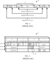
- FIG. 2 shows an example construction of a transaction 50 (e.g., transaction 20, 30 or 40 from FIG. 1 ).
- the transaction 50 includes a core section 52 of a Transaction Layer Packet (TLP) from an application executed by a Master 12 (see FIG. 1 ).
- TLP Transaction Layer Packet
- the TLP includes a header 54 and a data 56.
- a cyclical redundancy check (CRC) may also be added as an Error CRC (ECRC) 58.
- the transaction layer may be further encapsulated by a data link layer with a sequence number 60 and a Link CRC (LCRC) 62.
- a Physical (PHY) layer further encapsulates the encapsulated TLP with a start packet 70 and an end packet 72 to facilitate asynchronous communication of the transaction 50.
- FIG. 1 shows an example construction of a transaction 50 (e.g., transaction 20, 30 or 40 from FIG. 1 ).
- the transaction 50 includes a core section 52 of a Transaction Layer Pack
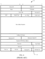
- the header 54 includes a current (or completion) status field 80 in Byte 6, bits 7:5 of the header 54.
- the current status field 80 may indicate a Successful Completion (SC) of a transaction, an Unsupported Request (UR), a Configuration Request Retry Status (CRS) or a Completer Abort (CA) for example, as an indication of a completion packet error.
- the current status field 80 may be returned as an acknowledgement to an MRd, shown as CpID 46, 34 or 24 in FIG. 1 .
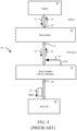
- FIG. 4 with continued reference to FIG. 1 further illustrates a context within which the disclosed embodiments of the CTOR may be used.
- the PCIe system 90 does not receive a timely response from the PCIe EP 18 to a memory read request MRd 42, thus triggering a CTO 92 after a time duration (or timeout limit).
- the Root Complex 16 reports the CTO 92, which results in an AXI error on an AXI bus.
- This AXI bus error may be treated as a System Error (SError), particularly when the Master is implemented with an ARM core. Consequently, the PCIe system 90 may completely shut down (e.g. "crash") without knowledge of the offending transaction or Master from which it issued in the case of multiple Masters.
- SError System Error
- FIG. 5 shows a PCIe system 100, in accordance with an embodiment of the present disclosure.
- the system 100 includes a plurality of Masters 102a, 102b and 102c (generally 102). Each Master 102 communicates with the Interconnect 106 with a respective transaction 104a, 104b and 104c (generally 104).
- the Interconnect 106 communicates with a PCIe controller 110 with a transaction 108.
- the PCIe controller 100 communicates with at least one PCIe EP 114 with a transaction 112.
- the TLP packet is issued by a respective Master 102 to the PCIe EP 114 as a memory read request 116.
- the MRd 116 is one of many packetized requests chosen for ease of illustration.
- the TLP packet may be an IO Write Request (IOWr) for example.
- the CTO 120 is monitored by a transmission monitor (TX Monitor) 122 and various error attributes, including but not limited to a Master ID of the Master that issued the offending transaction and a transaction address of the transaction, are stored in a CTOR 124.
- the stored error attributes are accessible by the PCIe controller 110, whose contents may be read by any Master 102 through a memory map.
- FIG. 6 shows an embodiment of a configuration space header 130 of a PCIe controller 110.
- the configuration space header 130 includes a capability pointer 132, which provides an address pointer to a plurality of capability pointers further described in FIG. 7 and FIG. 8.
- FIG. 7 shows a data structure of a configuration space 140 with CTOR capability, in accordance with an embodiment of the present disclosure.
- a first double word (DW0) (e.g., 32 bits), includes a Capability ID 142, linked to next capability pointer 144.
- the next capability pointer 144 is further linked to a next capability (e.g., a CTOR control register 146), thus forming a link list of capability pointers.
- the CTOR control register 146 may be part of the link list of DW0.
- a 16-bit field is allocated in DW1 to store the Master ID 148.
- a second 16-bit field of DW1 is a reserved field 150.
- a 32-bit field of DW2 stores the CTO address 152 of the offending transaction.
- FIG. 8 shows a data structure of a configuration space 160 with CTOR capability, in accordance with an embodiment of the present disclosure.
- FIG. 8 is similar to FIG. 7 apart from an additional 32-bit field of DW3 to store an upper half of the CTO address 162, when a 64-bit addressing scheme is used.
- FIG. 9 shows a data structure of the CTOR control register 146 further shown in FIG. 7 and FIG. 8 , in accordance with an embodiment of the present disclosure.
- the CTOR control register 146 may be scannable by the host software running on a Master 102.
- the first byte of the CTOR control register 146 stores a CTOR Enable 172. If CTOR Enable 172 is enabled (e.g., set to logical "1" in one embodiment), then the CTOR capability is supported. If CTOR Enable 172 is not enabled, then the configuration space 140 or 160 is not available, thereby providing backward capability to legacy PCIe systems.
- the second byte of the CTOR control register 146 stores a 64-bit Address Enable 174 (e.g., two double words). If the 64-bit Address Enable is enabled (e.g., set to logical "1" in one embodiment), then the data structure of FIG. 8 is used, otherwise the data structure of FIG. 7 is used.
- the third, fourth and fifth bytes of the CTOR control register 146 define a FIFO Length 176 of the First In First Out (FIFO).
- the FIFO provides further configuration of the address space used to store Master ID and CTO address. In one embodiment, the ten bytes of the CTOR control register 146 are reserved.
- FIG. 10 shows an embodiment 180 of a method to retrieve transaction address resulting in PCIe completion timeout.
- a PCIe controller 110 is monitored (e.g., with a Master 102) to detect a CTO 120.
- a Master ID 148 and a transaction address 152 are stored in a configuration space (e.g., the FIFO of the configuration space 140) in response to detecting the CTO 120.
- the Master 102 identified by the Master ID 148 responds to the CTO 120 (e.g., by terminating an application running on the Master 102 or avoiding an access associated with the transaction 152).
- FIG. 11 shows an embodiment 190 of a method to retrieve transaction address resulting in PCIe completion packet error.
- a PCIe controller 110 is monitored (e.g., with a Master 102) to detect a completion packet error.
- an error attribute of a transaction is stored in a configuration space (e.g., the FIFO of the configuration space 140) in response to detecting the completion packet error.
- the Master 102 identified by the Master ID 148 responds to the completion packet error (e.g., by terminating an application running on the Master 102 or avoiding an access associated with the transaction 152).
- FIG. 12 shows an embodiment 200 of a method to retrieve transaction address resulting in PCIe completion timeout.
- a configuration space 140 is configured with a CTOR control register 146.
- a Master ID 148 and a transaction address 152 are stored in a configuration space (e.g., the FIFO of the configuration space 140) in response to detecting the CTO 120 transmitted from a PCIe controller 110.
- the Master 102 identified by the Master ID 148 responds to the CTO 120 (e.g., by terminating an application running on the Master 102 or avoiding an access associated with the transaction 152).
- a method to retrieve transaction address resulting in PCIe completion timeout includes monitoring a Peripheral Component Interconnect Express (PCIe) controller to detect a Completion Timeout (CTO) transmitted therefrom.
- PCIe Peripheral Component Interconnect Express
- CTO Completion Timeout
- a Master Identification (ID) of a Master and a transaction address of a transaction are stored in a configuration space, in response to detecting the CTO, wherein the transaction originates from the Master and the CTO is signaled in response to the transaction.
- the CTO is responded to with the Master identified by the Master ID in the configuration space.
- a method to retrieve transaction address resulting in PCIe completion timeout comprises monitoring a Peripheral Component Interconnect Express (PCIe) controller to detect a Completion Timeout (CTO) transmitted therefrom.
- PCIe Peripheral Component Interconnect Express
- CTO Completion Timeout
- a Master Identification (ID) of a Master and a transaction address of a transaction are stored in a configuration space, in response to detecting the CTO, wherein the transaction originates from the Master and the CTO is signaled in response to the transaction.
- the CTO is responded to with the Master identified by the Master ID in the configuration space.
- the configuration space is configured by a Completion Timeout Reporting (CTOR) control register.
- the CTOR enables storing the Master ID and the transaction address in the configuration space by a setting of an enable bit of the CTOR.
- the CTOR configures a storage width of the transaction address in the configuration space by a setting of an address width bit of the CTOR.
- the CTOR configures a length of a First In First Out (FIFO) register in the configuration space by a setting of a plurality of FIFO length bits of the CTOR, wherein the FIFO register is configured to store a plurality of error attributes received from the PCIe controller.
- FIFO First In First Out
- a plurality of error attributes are stored in the configuration space.
- the response comprises terminating an application of the Master, wherein the transaction issues from the application.
- the response comprises preventing further access to a memory space related to the transaction.
- the transaction is a non-posted transaction and the CTO is transmitted by the PCIe controller in response to the PCIe controller not receiving a completion packet after a time duration.
- Performing the response with the Master comprises performing the response with an Advanced Reduced Instruction Set Computer Machine (ARM) core.
- ARM Advanced Reduced Instruction Set Computer Machine
- a method to retrieve transaction address resulting in PCIe completion packet error comprises monitoring a Peripheral Component Interconnect Express (PCIe) controller to detect a completion packet error transmitted therefrom.
- PCIe Peripheral Component Interconnect Express
- An error attribute of a transaction issued by a Master is stored in a configuration space, in response to detecting the CTO. The transaction is responded to with the Master.
- the error attributes comprise a Master Identification (ID) of the Master and a transaction address of the transaction.
- the configuration space is configured by a Completion Timeout Reporting (CTOR) control register.
- the response comprises terminating an application of the Master, wherein the transaction issues from the application.
- the response comprises preventing further access to a memory space related to the transaction.
- a method to retrieve transaction address resulting in PCIe completion timeout comprises configuring a configuration space with a Completion Timeout Reporting (CTOR) control register.
- a Master Identification (ID) of a Master and a transaction address of a transaction are stored in a configuration space, in response to detecting a Completion Timeout (CTO) transmitted from a Peripheral Component Interconnect Express (PCIe) controller, wherein the transaction originates from the Master.
- CTO Completion Timeout
- PCIe Peripheral Component Interconnect Express
- the CTOR enables storing the Master ID and the transaction address in the configuration space by a setting of an enable bit of the CTOR.
- the CTOR configures a storage width of the transaction address in the configuration space by a setting of an address width bit of the CTOR.
- the CTOR configures a length of a First In First Out (FIFO) register in the configuration space by a setting of a plurality of FIFO length bits of the CTOR, wherein the FIFO register is configured to store a plurality of error attributes received from the PCIe controller.
- the transaction is a non-posted transaction and the CTO is transmitted by the PCIe controller in response to the PCIe controller not receiving a completion packet after a time duration.
Landscapes
- Engineering & Computer Science (AREA)
- Theoretical Computer Science (AREA)
- Physics & Mathematics (AREA)
- General Engineering & Computer Science (AREA)
- General Physics & Mathematics (AREA)
- Quality & Reliability (AREA)
- Information Transfer Systems (AREA)
- Communication Control (AREA)
Applications Claiming Priority (1)
| Application Number | Priority Date | Filing Date | Title |
|---|---|---|---|
| IN202211066158 | 2022-11-18 |
Publications (1)
| Publication Number | Publication Date |
|---|---|
| EP4372575A1 true EP4372575A1 (de) | 2024-05-22 |
Family
ID=88833995
Family Applications (1)
| Application Number | Title | Priority Date | Filing Date |
|---|---|---|---|
| EP23209377.3A Pending EP4372575A1 (de) | 2022-11-18 | 2023-11-13 | Verfahren zum abrufen einer transaktionsadresse als ergebnis eines unkorrigierbaren pcie-fehlers |
Country Status (2)
| Country | Link |
|---|---|
| US (1) | US12271260B2 (de) |
| EP (1) | EP4372575A1 (de) |
Citations (3)
| Publication number | Priority date | Publication date | Assignee | Title |
|---|---|---|---|---|
| US20150281044A1 (en) * | 2014-03-31 | 2015-10-01 | Fujitsu Limited | Information processing device that generates packet including first and second identifiers, transmission and reception device, and control method of information processing device |
| US9170911B1 (en) * | 2013-07-09 | 2015-10-27 | Altera Corporation | Protocol error monitoring on an interface between hard logic and soft logic |
| US11048569B1 (en) * | 2017-06-27 | 2021-06-29 | Amazon Technologies, Inc. | Adaptive timeout mechanism |
Family Cites Families (13)
| Publication number | Priority date | Publication date | Assignee | Title |
|---|---|---|---|---|
| US6625683B1 (en) * | 1999-08-23 | 2003-09-23 | Advanced Micro Devices, Inc. | Automatic early PCI transaction retry |
| US7389379B1 (en) * | 2005-04-25 | 2008-06-17 | Network Appliance, Inc. | Selective disk offlining |
| US20060277444A1 (en) * | 2005-06-03 | 2006-12-07 | Nicholas Holian | Recordation of error information |
| US8959288B1 (en) * | 2010-07-29 | 2015-02-17 | Violin Memory, Inc. | Identifying invalid cache data |
| US8788873B2 (en) * | 2011-04-14 | 2014-07-22 | Cisco Technology, Inc. | Server input/output failover device serving highly available virtual devices |
| US8924607B1 (en) * | 2013-10-07 | 2014-12-30 | Nimble Storage, Inc. | Methods and systems for I/O cancellation using memory swap |
| JP6427979B2 (ja) | 2014-06-19 | 2018-11-28 | 富士通株式会社 | 原因特定方法、原因特定プログラム、情報処理システム |
| US10924538B2 (en) * | 2018-12-20 | 2021-02-16 | The Boeing Company | Systems and methods of monitoring software application processes |
| US11169713B2 (en) * | 2019-10-03 | 2021-11-09 | Landis+Gyr Innovations, Inc. | Restricting write cycles to extend the lifetime of nonvolatile memory |
| US11175977B2 (en) | 2020-01-14 | 2021-11-16 | Nxp Usa, Inc. | Method and system to detect failure in PCIe endpoint devices |
| US11264079B1 (en) * | 2020-12-18 | 2022-03-01 | Micron Technology, Inc. | Apparatuses and methods for row hammer based cache lockdown |
| US11693739B2 (en) * | 2021-04-09 | 2023-07-04 | International Business Machines Corporation | Hang detection and remediation in a multi-threaded application process |
| US12282391B2 (en) * | 2022-09-26 | 2025-04-22 | Dell Products, L.P. | Systems and methods for error recovery in rebootless firmware updates |
-
2023
- 2023-06-05 US US18/328,927 patent/US12271260B2/en active Active
- 2023-11-13 EP EP23209377.3A patent/EP4372575A1/de active Pending
Patent Citations (3)
| Publication number | Priority date | Publication date | Assignee | Title |
|---|---|---|---|---|
| US9170911B1 (en) * | 2013-07-09 | 2015-10-27 | Altera Corporation | Protocol error monitoring on an interface between hard logic and soft logic |
| US20150281044A1 (en) * | 2014-03-31 | 2015-10-01 | Fujitsu Limited | Information processing device that generates packet including first and second identifiers, transmission and reception device, and control method of information processing device |
| US11048569B1 (en) * | 2017-06-27 | 2021-06-29 | Amazon Technologies, Inc. | Adaptive timeout mechanism |
Non-Patent Citations (1)
| Title |
|---|
| ANONYMOUS: "INTEL DATA STREAMING ACCELERATOR ARCHITECTURE SPECIFICATION", 1 September 2022 (2022-09-01), XP093004343, Retrieved from the Internet <URL:https://cdrdv2-public.intel.com/671116/341204-intel-data-streaming-accelerator-spec.pdf> [retrieved on 20221202] * |
Also Published As
| Publication number | Publication date |
|---|---|
| US20240168842A1 (en) | 2024-05-23 |
| US12271260B2 (en) | 2025-04-08 |
Similar Documents
| Publication | Publication Date | Title |
|---|---|---|
| US6157975A (en) | Apparatus and method for providing an interface to a compound Universal Serial Bus controller | |
| KR100290943B1 (ko) | 유니버설 시리얼 버스 제어 이전을 처리하는 장치 및 방법 | |
| US4763249A (en) | Bus device for use in a computer system having a synchronous bus | |
| US5115499A (en) | Shared computer resource allocation system having apparatus for informing a requesting computer of the identity and busy/idle status of shared resources by command code | |
| US7849242B2 (en) | PCI express-compatible controller and interface that provides PCI express functionality and flash memory operations to host device | |
| EP0139563B1 (de) | Steuermechanismus für Mehrprozessorsystem | |
| EP0138676B1 (de) | Wiederholungsmechanismus zur Steuerungsfreigabe eines Übertragungsweges in einem digitalen Rechnersystem | |
| US6105080A (en) | Host adapter DMA controller with automated host reply capability | |
| CN118642993A (zh) | dToF智能模组通信方法、装置、dToF智能模组及存储介质 | |
| WO2001006711A1 (fr) | Controleur de transfert de donnees et dispositif electronique | |
| US20090271532A1 (en) | Early header CRC in data response packets with variable gap count | |
| US5546587A (en) | Decentralized bus arbitration system which continues to assert bus request signal to preclude other from asserting bus request signal until information transfer on the bus has been completed | |
| EP4372575A1 (de) | Verfahren zum abrufen einer transaktionsadresse als ergebnis eines unkorrigierbaren pcie-fehlers | |
| KR910001788B1 (ko) | 다중 프로세서 시스템용 메세지 전송 인터럽팅 장치 및 이의 실행방법 | |
| US6693905B1 (en) | Data exchange unit | |
| US20090268736A1 (en) | Early header CRC in data response packets with variable gap count | |
| CN119003420A (zh) | 服务器、访问双列直插式内存控制模块的装置及集成电路 | |
| EP4260197B1 (de) | Tags für anforderungspakete in einer netzwerkkommunikationsverbindung | |
| JP2009502072A (ja) | FlexRay通信モジュール及びFlexRay通信制御装置、並びにFlexRay通信接続とFlexRay加入者装置との間でメッセージを伝送する方法 | |
| US20050144331A1 (en) | On-chip serialized peripheral bus system and operating method thereof | |
| JPS6035698B2 (ja) | デ−タ処理システム | |
| US20090268727A1 (en) | Early header CRC in data response packets with variable gap count | |
| CN112346922B (zh) | 服务器装置及其通讯协议方法 | |
| CN119988271A (zh) | 半导体器件和半导体系统 | |
| CN120429251A (zh) | 数据传输方法、装置和芯片 |
Legal Events
| Date | Code | Title | Description |
|---|---|---|---|
| PUAI | Public reference made under article 153(3) epc to a published international application that has entered the european phase |
Free format text: ORIGINAL CODE: 0009012 |
|
| STAA | Information on the status of an ep patent application or granted ep patent |
Free format text: STATUS: THE APPLICATION HAS BEEN PUBLISHED |
|
| AK | Designated contracting states |
Kind code of ref document: A1 Designated state(s): AL AT BE BG CH CY CZ DE DK EE ES FI FR GB GR HR HU IE IS IT LI LT LU LV MC ME MK MT NL NO PL PT RO RS SE SI SK SM TR |
|
| STAA | Information on the status of an ep patent application or granted ep patent |
Free format text: STATUS: REQUEST FOR EXAMINATION WAS MADE |
|
| 17P | Request for examination filed |
Effective date: 20241122 |
|
| RBV | Designated contracting states (corrected) |
Designated state(s): AL AT BE BG CH CY CZ DE DK EE ES FI FR GB GR HR HU IE IS IT LI LT LU LV MC ME MK MT NL NO PL PT RO RS SE SI SK SM TR |
|
| STAA | Information on the status of an ep patent application or granted ep patent |
Free format text: STATUS: EXAMINATION IS IN PROGRESS |
|
| 17Q | First examination report despatched |
Effective date: 20251022 |