EP4369888A1 - Foldable display device and method for manufacturing same - Google Patents
Foldable display device and method for manufacturing same Download PDFInfo
- Publication number
- EP4369888A1 EP4369888A1 EP22837894.9A EP22837894A EP4369888A1 EP 4369888 A1 EP4369888 A1 EP 4369888A1 EP 22837894 A EP22837894 A EP 22837894A EP 4369888 A1 EP4369888 A1 EP 4369888A1
- Authority
- EP
- European Patent Office
- Prior art keywords
- laser
- support member
- slits
- disposed
- layer
- Prior art date
- Legal status (The legal status is an assumption and is not a legal conclusion. Google has not performed a legal analysis and makes no representation as to the accuracy of the status listed.)
- Pending
Links
Images









Classifications
-
- G—PHYSICS
- G06—COMPUTING OR CALCULATING; COUNTING
- G06F—ELECTRIC DIGITAL DATA PROCESSING
- G06F1/00—Details not covered by groups G06F3/00 - G06F13/00 and G06F21/00
- G06F1/16—Constructional details or arrangements
- G06F1/1613—Constructional details or arrangements for portable computers
- G06F1/1633—Constructional details or arrangements of portable computers not specific to the type of enclosures covered by groups G06F1/1615 - G06F1/1626
- G06F1/1637—Details related to the display arrangement, including those related to the mounting of the display in the housing
- G06F1/1652—Details related to the display arrangement, including those related to the mounting of the display in the housing the display being flexible, e.g. mimicking a sheet of paper, or rollable
-
- G—PHYSICS
- G06—COMPUTING OR CALCULATING; COUNTING
- G06F—ELECTRIC DIGITAL DATA PROCESSING
- G06F1/00—Details not covered by groups G06F3/00 - G06F13/00 and G06F21/00
- G06F1/16—Constructional details or arrangements
- G06F1/1613—Constructional details or arrangements for portable computers
- G06F1/1633—Constructional details or arrangements of portable computers not specific to the type of enclosures covered by groups G06F1/1615 - G06F1/1626
- G06F1/1637—Details related to the display arrangement, including those related to the mounting of the display in the housing
- G06F1/1641—Details related to the display arrangement, including those related to the mounting of the display in the housing the display being formed by a plurality of foldable display components
-
- G—PHYSICS
- G09—EDUCATION; CRYPTOGRAPHY; DISPLAY; ADVERTISING; SEALS
- G09F—DISPLAYING; ADVERTISING; SIGNS; LABELS OR NAME-PLATES; SEALS
- G09F9/00—Indicating arrangements for variable information in which the information is built-up on a support by selection or combination of individual elements
- G09F9/30—Indicating arrangements for variable information in which the information is built-up on a support by selection or combination of individual elements in which the desired character or characters are formed by combining individual elements
- G09F9/301—Indicating arrangements for variable information in which the information is built-up on a support by selection or combination of individual elements in which the desired character or characters are formed by combining individual elements flexible foldable or roll-able electronic displays, e.g. thin LCD, OLED
-
- H—ELECTRICITY
- H10—SEMICONDUCTOR DEVICES; ELECTRIC SOLID-STATE DEVICES NOT OTHERWISE PROVIDED FOR
- H10K—ORGANIC ELECTRIC SOLID-STATE DEVICES
- H10K50/00—Organic light-emitting devices
- H10K50/80—Constructional details
- H10K50/84—Passivation; Containers; Encapsulations
- H10K50/844—Encapsulations
-
- B—PERFORMING OPERATIONS; TRANSPORTING
- B32—LAYERED PRODUCTS
- B32B—LAYERED PRODUCTS, i.e. PRODUCTS BUILT-UP OF STRATA OF FLAT OR NON-FLAT, e.g. CELLULAR OR HONEYCOMB, FORM
- B32B5/00—Layered products characterised by the non- homogeneity or physical structure, i.e. comprising a fibrous, filamentary, particulate or foam layer; Layered products characterised by having a layer differing constitutionally or physically in different parts
- B32B5/02—Layered products characterised by the non- homogeneity or physical structure, i.e. comprising a fibrous, filamentary, particulate or foam layer; Layered products characterised by having a layer differing constitutionally or physically in different parts characterised by structural features of a fibrous or filamentary layer
- B32B5/04—Layered products characterised by the non- homogeneity or physical structure, i.e. comprising a fibrous, filamentary, particulate or foam layer; Layered products characterised by having a layer differing constitutionally or physically in different parts characterised by structural features of a fibrous or filamentary layer characterised by a layer being specifically extensible by reason of its structure or arrangement, e.g. by reason of the chemical nature of the fibres or filaments
-
- B—PERFORMING OPERATIONS; TRANSPORTING
- B32—LAYERED PRODUCTS
- B32B—LAYERED PRODUCTS, i.e. PRODUCTS BUILT-UP OF STRATA OF FLAT OR NON-FLAT, e.g. CELLULAR OR HONEYCOMB, FORM
- B32B5/00—Layered products characterised by the non- homogeneity or physical structure, i.e. comprising a fibrous, filamentary, particulate or foam layer; Layered products characterised by having a layer differing constitutionally or physically in different parts
- B32B5/22—Layered products characterised by the non- homogeneity or physical structure, i.e. comprising a fibrous, filamentary, particulate or foam layer; Layered products characterised by having a layer differing constitutionally or physically in different parts characterised by the presence of two or more layers which are next to each other and are fibrous, filamentary, formed of particles or foamed
- B32B5/24—Layered products characterised by the non- homogeneity or physical structure, i.e. comprising a fibrous, filamentary, particulate or foam layer; Layered products characterised by having a layer differing constitutionally or physically in different parts characterised by the presence of two or more layers which are next to each other and are fibrous, filamentary, formed of particles or foamed one layer being a fibrous or filamentary layer
- B32B5/26—Layered products characterised by the non- homogeneity or physical structure, i.e. comprising a fibrous, filamentary, particulate or foam layer; Layered products characterised by having a layer differing constitutionally or physically in different parts characterised by the presence of two or more layers which are next to each other and are fibrous, filamentary, formed of particles or foamed one layer being a fibrous or filamentary layer another layer next to it also being fibrous or filamentary
-
- G—PHYSICS
- G06—COMPUTING OR CALCULATING; COUNTING
- G06F—ELECTRIC DIGITAL DATA PROCESSING
- G06F1/00—Details not covered by groups G06F3/00 - G06F13/00 and G06F21/00
- G06F1/16—Constructional details or arrangements
- G06F1/1613—Constructional details or arrangements for portable computers
- G06F1/1615—Constructional details or arrangements for portable computers with several enclosures having relative motions, each enclosure supporting at least one I/O or computing function
- G06F1/1616—Constructional details or arrangements for portable computers with several enclosures having relative motions, each enclosure supporting at least one I/O or computing function with folding flat displays, e.g. laptop computers or notebooks having a clamshell configuration, with body parts pivoting to an open position around an axis parallel to the plane they define in closed position
-
- G—PHYSICS
- G06—COMPUTING OR CALCULATING; COUNTING
- G06F—ELECTRIC DIGITAL DATA PROCESSING
- G06F1/00—Details not covered by groups G06F3/00 - G06F13/00 and G06F21/00
- G06F1/16—Constructional details or arrangements
- G06F1/1613—Constructional details or arrangements for portable computers
- G06F1/1633—Constructional details or arrangements of portable computers not specific to the type of enclosures covered by groups G06F1/1615 - G06F1/1626
- G06F1/1637—Details related to the display arrangement, including those related to the mounting of the display in the housing
-
- G—PHYSICS
- G06—COMPUTING OR CALCULATING; COUNTING
- G06F—ELECTRIC DIGITAL DATA PROCESSING
- G06F1/00—Details not covered by groups G06F3/00 - G06F13/00 and G06F21/00
- G06F1/16—Constructional details or arrangements
- G06F1/1613—Constructional details or arrangements for portable computers
- G06F1/1633—Constructional details or arrangements of portable computers not specific to the type of enclosures covered by groups G06F1/1615 - G06F1/1626
- G06F1/1637—Details related to the display arrangement, including those related to the mounting of the display in the housing
- G06F1/1643—Details related to the display arrangement, including those related to the mounting of the display in the housing the display being associated to a digitizer, e.g. laptops that can be used as penpads
-
- H—ELECTRICITY
- H10—SEMICONDUCTOR DEVICES; ELECTRIC SOLID-STATE DEVICES NOT OTHERWISE PROVIDED FOR
- H10K—ORGANIC ELECTRIC SOLID-STATE DEVICES
- H10K59/00—Integrated devices, or assemblies of multiple devices, comprising at least one organic light-emitting element covered by group H10K50/00
- H10K59/40—OLEDs integrated with touch screens
-
- H—ELECTRICITY
- H10—SEMICONDUCTOR DEVICES; ELECTRIC SOLID-STATE DEVICES NOT OTHERWISE PROVIDED FOR
- H10K—ORGANIC ELECTRIC SOLID-STATE DEVICES
- H10K59/00—Integrated devices, or assemblies of multiple devices, comprising at least one organic light-emitting element covered by group H10K50/00
- H10K59/60—OLEDs integrated with inorganic light-sensitive elements, e.g. with inorganic solar cells or inorganic photodiodes
-
- Y—GENERAL TAGGING OF NEW TECHNOLOGICAL DEVELOPMENTS; GENERAL TAGGING OF CROSS-SECTIONAL TECHNOLOGIES SPANNING OVER SEVERAL SECTIONS OF THE IPC; TECHNICAL SUBJECTS COVERED BY FORMER USPC CROSS-REFERENCE ART COLLECTIONS [XRACs] AND DIGESTS
- Y02—TECHNOLOGIES OR APPLICATIONS FOR MITIGATION OR ADAPTATION AGAINST CLIMATE CHANGE
- Y02E—REDUCTION OF GREENHOUSE GAS [GHG] EMISSIONS, RELATED TO ENERGY GENERATION, TRANSMISSION OR DISTRIBUTION
- Y02E10/00—Energy generation through renewable energy sources
- Y02E10/50—Photovoltaic [PV] energy
- Y02E10/549—Organic PV cells
Definitions
- Embodiments of the invention relate to a foldable display device and a method of manufacturing the same.
- display devices are being applied to vari ous electronic devices such as smartphones, digital cameras, notebook computers, navigation devices, and smart televisions.
- a bendable display device in which a display area can be bent or a foldable display device in which a display area can be folded have been released recently.
- a display device supports a touch input using a user's body part (e.g., a finger) and a touch input using an electronic pen (e.g., a stylus pen). Since the display device uses the touch input using the electronic pen, it can sense a touch input more precisely than when using only the touch input using the user's body part. In this case, if a metal support member is used to support a display panel of the foldable display device, the sensitivity of the touch input using the electronic pen may be reduced due to the metal support member.
- aspects of the present invention are to provide a foldable display device including a panel support member which can support a display panel while not reducing the sensitivity of a touch input using an electronic pen.
- aspects of the present invention are to provide a method of manufacturing a foldable display device including a panel support member which can support a display panel while not reducing the sensitivity of a touch input using an electronic pen.
- An embodiment of the invention provides a foldable display device including a display panel which comprises a folding area, a first non-folding area disposed on a side of the folding area, and a second non-folding area disposed on the other side of the folding area, and a panel support member which is disposed on a surface of the display panel and includes a plurality of slits extending in a first direction.
- the panel support member includes a first layer which has a first fiber yarn extending in a second direction intersecting the first direction, a second layer which has a second fiber yarn extending in the first direction, and a third layer which has a third fiber yarn extending in the second direction.
- a thickness of the second layer may be greater than a thickness of the first layer and a thickness of the third layer.
- the second direction may be parallel to a first folding line corresponding to a boundary between the folding area and the first non-folding area and a second folding line corresponding to a boundary between the folding area and the second non-folding area.
- the slits may be disposed in the folding area.
- the slits may include first slits disposed in a first column, second slits disposed in a second column and third slits disposed in a third column, and the second slits are shifted in the first direction compared with the first slits and the third slits.
- a lower half of any one of the first slits, an upper half of any one of the second slits, and a lower half of any one of the third slits may overlap each other in the second direction.
- An embodiment of the invention provides a foldable display device including a display panel which comprises an alignment mark, and a panel support member which is disposed on a surface of the display panel and comprises a notch extending in a thickness direction of the display panel.
- the panel support member includes a first layer which has a first fiber yarn extending in a second direction intersecting a first direction, a second layer which has a second fiber yarn extending in the first direction, and a third layer which has a third fiber yarn extending in the second direction.
- the alignment mark may overlap the notch in the thickness direction of the display panel.
- the notch may be shaped like a groove or a ditch recessed from a side surface of the panel support member.
- the foldable display device may further include an optical device which senses light.
- the display panel may include a light transmitting area which overlaps the optical device in the thickness direction of the display panel, and the panel support member may include a through hole which overlaps the light transmitting area in the thickness direction of the display panel.
- the area of the light transmitting area may be larger than the area of the through hole.
- An embodiment of the invention provides a method of manufacturing a foldable display device including machining edges of a panel support member by using a laser, forming a lattice pattern in a folding area of the panel support member by using the laser, attaching a digitizer member onto a surface of the panel support member, and attaching the panel support member onto a surface of a display panel.
- a pulse period of the laser may be several to hundreds of nanoseconds, several to hundreds of picoseconds, or several to hundreds of femtoseconds.
- a scan speed of the laser may be 800 mm/s or less
- a pulse repetition rate of the laser may be 200 kHz or less
- power of the laser may be 13 W or less.
- the laser when the laser is an ultraviolet laser and the pulse period of the laser may be several to hundreds of picoseconds or several to hundreds of femtoseconds, the scan speed of the laser may be 5000 mm/s or less, the pulse repetition rate of the laser may be 3000 kHz or less, and the power of the laser may be 50 W or less.
- the scan speed of the laser may be 1000 mm/s or less
- the pulse repetition rate of the laser may be 2000 kHz or less
- the power of the laser may be 20 W or less.
- the method may further include forming a through hole passing through the panel support member by using the laser.
- At least one notch disposed on a side surface of the panel support member may be machined.
- the lattice pattern may include a plurality of slits which are defined by a plurality of bars and extend in a first direction.
- the slits comprise a first slit, a second slit, and a third slit disposed in a second direction intersecting the first direction
- the forming of the lattice pattern in the folding area of the panel support member by using the laser may include machining the first slit, skipping the second slit, and machining the third slit.
- the slits may include a plurality of first slits disposed in the first direction
- the forming of the lattice pattern in the folding area of the panel support member by using the laser may include machining any one of the first slits, skipping a first slit neighboring the machined first slit in the first direction, and machining a first slit neighboring the skipped first slit in the first direction.
- a panel support member is included.
- the panel support member is disposed on a rear surface of a display panel and is a rigid member that is not easily changed in shape or volume by external pressure. Since the panel support member is made of a polymer including carbon fibers or glass fibers, a magnetic field or electromagnetic signal of a digitizer member can pass through the panel support member. Therefore, the panel support member can stably support the display panel while not reducing the touch sensitivity of the digitizer member.
- the energy of a laser applied to a panel support member can be reduced by adjusting a pulse period of the laser, a scan speed of the laser, a pulse repetition rate of the laser, and power of the laser. Therefore, since thermal energy generated on a cut surface of the panel support member can be reduced, it is possible to prevent a resin holding fiber yarn from falling off or cracking due to the thermal energy. Accordingly, it is possible to prevent a cut part of the fiber yarn from remaining as a byproduct on the cut surface of the panel support member.
- the machining order of slits may be determined such that the slits neighboring each other in a first direction and a second direction are not successively machined. Therefore, an area in which thermal energy due to a laser is accumulated can be removed from a plurality of bars that define the slits. Hence, it is possible to prevent a resin holding fiber yarn from falling off or from cracking due to the thermal energy. Accordingly, it is possible to prevent a cut part of the fiber yarn from remaining as a byproduct on a cut surface of the panel support member.
- one element or layer 'on' another element or layer includes both of a case where one element or layer is disposed immediately above another element or layer and a case where one element or layer is disposed above another element or layer with the other layer or element interposed therebetween.
- the same components will be denoted by the same reference numerals.
- the shape, size, ratio, angle, number and the like shown in the drawings to illustrate the embodiments of the present disclosure are only for illustration and are not limited to the contents shown in the drawings.
- first means “first”, “second”, and the like are used to describe various components, but these components are not limited by these terms. These terms are used only in order to distinguish one component from another component. Therefore, a first component mentioned below may be a second component within the technical spirit of the present disclosure.
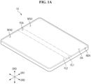
- FIGS. 1A and 1B are perspective views of a foldable display device 10 according to an embodiment.
- FIG. 1A illustrates a first state in which the foldable display device 10 is not folded at folding lines FL1 and FL2, and FIG. 1B illustrates a second state in which the foldable display device 10 is folded at the folding lines FL1 and FL2.
- the foldable display device 10 is a device for displaying moving images or still images.
- the foldable display device 10 may be used as a display screen in portable electronic devices such as mobile phones, smartphones, tablet personal computers (PCs), smart watches, watch phones, mobile communication terminals, electronic notebooks, electronic books, portable multimedia players (PMPs), navigation devices and ultra-mobile PCs (UMPCs), as well as in various products such as televisions, notebook computers, monitors, billboards and the Internet of things (IoT).
- portable electronic devices such as mobile phones, smartphones, tablet personal computers (PCs), smart watches, watch phones, mobile communication terminals, electronic notebooks, electronic books, portable multimedia players (PMPs), navigation devices and ultra-mobile PCs (UMPCs)
- portable multimedia players PMPs
- UMPCs ultra-mobile PCs
- a first direction DR1 may be a direction parallel to a side of the display device 10 when seen in plan view, for example, may be a horizontal direction of the display device 10.
- a second direction DR2 may be a direction parallel to another side in contact with the above side of the display device 10 when seen in plan view, for example, may be a vertical direction of the display device 10.
- a third direction DR3 may be a thickness direction of the display device 10.
- the planar shape of the display device 10 may be a quadrangular shape such as a rectangular shape. Each corner of the display device 10 may have a right-angled planar shape or a round planar shape.
- a front surface of the display device 10 may include two short sides disposed in the first direction DR1 and two long sides disposed in the second direction DR2.
- the display device 10 includes a display area DA and a non-display area NDA.
- the planar shape of the display area DA may follow the shape of the display device 10.
- the display area DA may also be rectangular in plan view.
- the display area DA may be an area which includes a plurality of pixels to display an image.
- the non-display area NDA may be an area which does not include pixels and thus does not display an image.
- the non-display area NDA may be disposed around the display area DA.
- the non-display area NDA may surround the display area DA, but embodiments of the present specification are not limited thereto.
- the display area DA may be partially surrounded by the non-display area NDA.
- the display device 10 may maintain both the first state which is an unfolded state and the second state which is a folded state.
- the display device 10 may be folded in an in-folding manner so that parts of the display area DA face each other as illustrated in FIG. 1B .
- parts of the front surface of the display device 10 may face each other when the display device 10 is folded.
- the display device 10 may be folded in an out-folding manner so that parts of a rear surface of the display device 10 face each other.
- the display device 10 may include a folding area FDA, a first non-folding area NFA1, and a second non-folding area NFA2.
- the folding area FDA may be an area in which the display device 10 is bent or folded.
- the first non-folding area NFA1 and the second non-folding area NFA2 may be areas in which the display device 10 is not bent or folded. That is, the first non-folding area NFA1 and the second non-folding area NFA2 may be flat areas of the display device 10.
- the first non-folding area NFA1 may be disposed on a side, e.g., a right side of the folding area FDA.
- the second non-folding area NFA2 may be disposed on the other side, e.g., a left side of the folding area FDA.
- the folding area FDA may be an area which is defined by a first folding line FL1 and a second folding line FL2 and an area in which the display device 10 is bent with a predetermined curvature.
- the first folding line FL1 may be a boundary between the folding area FDA and the first non-folding area NFA1
- the second folding line FL2 may be a boundary between the folding area FDA and the second non-folding area NFA2.
- the first folding line FL1 and the second folding line FL2 may extend in the first direction DR1 as illustrated in FIGS. 1A and 1B , in which case the display device 10 may be folded in the second direction DR2. Therefore, since a length of the display device 10 in the second direction DR2 can be reduced by about half, it may be easy for a user to carry the display device 10.
- a length of the folding area FDA in the second direction DR2 may be greater than a length of the folding area FDA in the first direction DR1.
- a length of the first non-folding area NFA1 in the second direction DR2 may be greater than a length of the first non-folding area NFA1 in the first direction DR1.
- a length of the second non-folding area NFA2 in the second direction DR2 may be greater than a length of the second non-folding area NFA2 in the first direction DR1.
- Each of the display area DA and the non-display area NDA may overlap at least one of the folding area FDA, the first non-folding area NFA1, and the second non-folding area NFA2.
- each of the display area DA and the non-display area NDA overlaps the folding area FDA, the first non-folding area NFA1, and the second non-folding area NFA2.
- FIGS. 2A and 2B are perspective views of a display device 10 according to an embodiment.
- FIG. 2A is a perspective view of the display device 10 according to the embodiment in an unfolded state.
- FIG. 2B is a perspective view of the display device 10 according to the embodiment in a folded state.
- FIGS. 2A and 2B is only different from the embodiment of FIGS. 1A and 1B in that a first folding line FL1 and a second folding line FL2 extend in the first direction DR1 and the display device 10 is folded in the second direction DR2 and thus that a length of the display device 10 in the second direction DR2 is reduced by about half. Therefore, in FIGS. 2A and 2B , a description of elements and features identical to those of the embodiment of FIGS. 1A and 1B will be omitted.
- a first non-folding area NFA1 may be disposed on a side, e.g., a lower side of a folding area FDA.
- a second non-folding area NFA2 may be disposed on the other side, e.g., an upper side of the folding area FDA.
- a length of the folding area FDA in the first direction DR1 may be greater than a length of the folding area FDA in the second direction DR2.
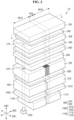
- FIG. 3 is an exploded perspective view of a display device 10 according to an embodiment.
- FIG. 4 is a side view of the display device 10 according to the embodiment.
- the display device 10 may include an upper protection member 100, a window member 200, a first adhesive member 300, a display panel 400, a panel protection member 500, an under-panel member 600, a panel support member 700, a second adhesive member 800, a digitizer member 900, a metal support member 1000, a buffer member 1100, and a third adhesive member 1200.
- the display panel 400 may be a panel that displays an image.
- the display panel 400 may be an organic light emitting display panel including an organic light emitting layer, a quantum dot light emitting display panel including a quantum dot light emitting layer, an inorganic light emitting display panel using an inorganic semiconductor element as a light emitting element, or a micro light emitting display panel using a micro light emitting diode as a light emitting element.
- a case where the display panel 400 is an organic light emitting display panel will be mainly described below, but embodiments of the present specification are not limited thereto.
- the display panel 400 may include a light transmitting area LTA overlapping an optical device OPD in the third direction DR3.
- the optical device OPD may be an optical sensor that senses light, for example, a camera sensor, a proximity sensor, or an illuminance sensor.
- the light transmitting area LTA may be a part of a display area DA.
- the light transmitting area LTA may include a transmitting area that can transmit light.
- the light transmitting area LTA may be a through hole that passes through the display panel 400.
- the light transmittance of the light transmitting area LTA may be higher than the light transmittance of the display area DA excluding the light transmitting area LTA.
- the density or integration degree of pixels in the light transmitting area LTA may be lower than the density or integration degree of pixels in the display area DA excluding the light transmitting area LTA.
- the number of pixels per unit area in the light transmitting area LTA may be smaller than the number of pixels per unit area in the display area DA excluding the light transmitting area LTA.
- pixels per inch (PPI) in the light transmitting area LTA may be smaller than PPI in the display area DA excluding the light transmitting area LTA.
- the window member 200 may be attached onto a front surface of the display panel 400 by the first adhesive member 300.
- the window member 200 may be made of a transparent material, for example, may be glass or plastic.
- the window member 200 may be ultra-thin glass (UTG) having a thickness of 0.1 mm or less or may be a transparent polyimide film.
- the first adhesive member 300 may be a transparent adhesive film or a transparent adhesive resin.
- the upper protection member 100 may be disposed on a front surface of the window member 200.
- the upper protection member 100 may be attached to the front surface of the window member 200.
- the upper protection member 100 may perform at least one of scattering prevention, shock absorption, dent prevention, fingerprint prevention, and anti-glare functions of the window member 200.
- a light blocking pattern may be formed on a rear surface of the upper protection member 100.
- the light blocking pattern may be disposed on or adjacent to edges of the upper protection member 100.
- the light blocking pattern may include a light blocking material that can block light.
- the light blocking pattern may be an inorganic black pigment such as carbon black, an organic block pigment, or an opaque metal material.
- the panel protection member 500 may be disposed on a rear surface of the display panel 400.
- the panel protection member 500 may support the display panel 400 and protect the rear surface of the display panel 400.
- the panel protection member 500 may be plastic such as polyethylene terephthalate (PET) or polyimide.
- PET polyethylene terephthalate
- the panel protection member 500 is disposed in a folding area FDA of the display device 10 in FIGS. 3 and 4 , embodiments of the present specification are not limited thereto.
- the panel protection member 500 may be removed from the folding area FDA of the display device 10 so that the display device 10 can be smoothly folded.
- the under-panel member 600 may be disposed on a rear surface of the panel protection member 500.
- the under-panel member 600 may include at least one of a light blocking layer for absorbing light incident from the outside, a buffer layer for absorbing external shock, and a heat dissipating layer for efficiently dissipating the heat of the display panel 400.
- the light blocking layer blocks transmission of light to prevent elements disposed under the light blocking layer, for example, the digitizer member 900 from being seen from above the display panel 400.
- the light blocking layer may include a light absorbing material such as a black pigment or a black dye.
- the buffer layer absorbs external shock to prevent the display panel 400 from being damaged.
- the buffer layer may be composed of a single layer or a plurality of layers.
- the buffer layer may be made of polymer resin such as polyurethane, polycarbonate, polypropylene or polyethylene or may be made of an elastic material such as rubber, a urethane-based material, or a sponge formed by foam molding an acrylic-based material.
- the heat dissipating layer may include a first heat dissipating layer including graphite or carbon nanotubes and a second heat dissipating layer made of a metal thin film (such as copper, nickel, ferrite or silver) capable of shielding electromagnetic waves and having excellent heat conductivity.
- a metal thin film such as copper, nickel, ferrite or silver
- the panel support member 700 may be disposed on a rear surface of the under-panel member 600.
- the panel support member 700 may be a rigid member that is not easily changed in shape or volume by external pressure.
- the panel support member 700 may be a polymer including carbon fibers or glass fibers.
- the panel support member 700 may include a lattice pattern disposed in the folding area FDA so that it can be easily bent in the folding area FDA.
- the panel support member 700 may include a through hole STH overlapping the optical device OPD in the third direction DR3.
- the through hole STH may overlap the light transmitting area LTA of the display panel 400 in the third direction DR3.
- the area of the through hole STH may be larger than the area of the light transmitting area LTA.
- the optical device OPD may sense light incident from a front surface of the display device 10 through the light transmitting area LTA and the through hole STH.
- the panel support member 700 will be described in detail with reference to FIGS. 6 through 11 .
- the digitizer member 900 may include a first digitizer member 910 and a second digitizer member 920.
- the first digitizer member 910 and the second digitizer member 920 may be disposed on a rear surface of the panel support member 700.
- the first digitizer member 910 and the second digitizer member 920 may be attached to the rear surface of the panel support member 700 by the second adhesive member 800.
- the second adhesive member 800 may be a pressure sensitive adhesive.
- the first digitizer member 910 and the second digitizer member 920 may not be disposed in the folding area FDA to reduce folding stress of the display device 10.
- the first digitizer member 910 may be disposed in a first non-folding area NFA1
- the second digitizer member 920 may be disposed in a second non-folding area NFA2.
- a gap between the first digitizer member 910 and the second digitizer member 920 may overlap the folding area FDA and may be smaller than a width of the folding area FDA.
- the width of the folding area FDA may be a length of the folding area FDA in the second direction (Y-axis direction).
- the first digitizer member 910 and the second digitizer member 920 may include electrode patterns for sensing approach or contact of an electronic pen such as a stylus pen that supports electromagnetic resonance (EMR).
- the first digitizer member 910 and the second digitizer member 920 may sense a magnetic field or electromagnetic signal emitted from the electronic pen based on the electrode patterns and determine a point, at which the sensed magnetic field or electromagnetic signal is greatest, as touch coordinates.
- Magnetic metal power may be disposed on a rear surface of the first digitizer member 910 and a rear surface of the second digitizer member 920.
- a magnetic field or an electromagnetic signal passing through the first digitizer member 910 and the second digitizer member 920 may flow into the magnetic metal powder. Therefore, due to the magnetic metal powder, it is possible to reduce the emission of the magnetic field or electromagnetic signal of the first digitizer member 910 and the second digitizer member 920 to a rear surface of the display device 10.
- the metal support member 1000 may include a first metal support member 1010 and a second metal support member 1020.
- the first metal support member 1010 may be disposed on the rear surface of the first digitizer member 910, and the second metal support member 1020 may be disposed on the rear surface of the second digitizer member 920.
- the first metal support member 1010 and the second metal support member 1020 may not be disposed in the folding area FDA to reduce folding stress of the display device 10.
- the first metal support member 1010 may be disposed in the first non-folding area NFA1
- the second metal support member 1020 may be disposed in the second non-folding area NFA2.
- a gap between the first metal support member 1010 and the second metal support member 1020 may overlap the folding area FDA and may be smaller than the width of the folding area FDA.
- the first metal support member 1010 and the second metal support member 1020 may include a material having high rigidity to support the first digitizer member 910 and the second digitizer member 920.
- the first metal support member 1010 and the second metal support member 1020 may include stainless steel such as SUS316.
- the buffer member 1100 may include a first buffer member 1110 and a second buffer member 1120.
- the first buffer member 1110 and the second buffer member 1120 may absorb external shock to prevent the panel support member 700 and the digitizer member 900 from being damaged.
- the first buffer member 1110 and the second buffer member 1120 may include an elastic material such as rubber, a urethane-based material, or a sponge formed by foam molding an acrylic-based material.
- the first buffer member 1110 may be disposed on a rear surface of the first metal support member 1010, and the second buffer member 1120 may be disposed on a rear surface of the second metal support member 1020.
- the first buffer member 1110 and the second buffer member 1120 may not be disposed in the folding area FDA to reduce folding stress of the display device 10.
- the first buffer member 1110 may be disposed in the first non-folding area NFA1, and the second buffer member 1120 may be disposed in the second non-folding area NFA2.
- a gap between the first buffer member 1110 and the second buffer member 1120 may overlap the folding area FDA and may be smaller than the width of the folding area FDA.
- the third adhesive member 1200 may be disposed on the rear surface of the first metal support member 1010 and the rear surface of the second metal support member 1020.
- the third adhesive member 1200 may be disposed on edges of the first metal support member 1010 and edges of the second metal support member 1020.
- the third adhesive member 1200 may surround the first buffer member 1110 and the second buffer member 1120.
- the third adhesive member 1200 may be a waterproof tape or a waterproof member for attaching the rear surface of the first metal support member 1010 to a front surface of a frame disposed on a rear surface of the buffer member 1100. Therefore, the third adhesive member 1200 may prevent moisture or dust from penetrating into the display device 10. That is, a waterproof and dustproof display device 10 can be provided.
- the third adhesive member 1200 may not surround the first buffer member 1110 and the second buffer member 1120 and may overlap, in the third direction DR3, a magnet for keeping the display device 10 folded.
- the third adhesive member 1200 may serve as a magnetic shielding member which can shield magnetism to prevent the digitizer member 900 or the display panel 400 from being affected by the magnetism of the magnet.
- the panel support member 700 may be disposed on the rear surface of the display panel 400 and may support the display panel 400 because it is a rigid member that is not easily changed in shape or volume by external pressure.
- the panel support member 700 is made of a polymer including carbon fibers or glass fibers, a magnetic field or electromagnetic signal of the digitizer member 900 can pass through the panel support member 700. Therefore, the panel support member 700 capable of supporting the display panel 400 while not reducing the touch sensitivity of the digitizer member 900 can be provided.
- the panel support member 700 since the panel support member 700 includes a lattice pattern disposed in the folding area FDA, it can be easily bent when the display device 10 is folded.
- FIG. 5 is a detailed cross-sectional view of an example of the display panel 400 of FIGS. 3 and 4 .
- a display layer DISL may be disposed on a substrate SUB.
- the display layer DISL may include a thin-film transistor layer TFTL, a light emitting element layer EML, and an encapsulation layer TFEL.
- the thin-film transistor layer TFTL may be disposed on the substrate SUB.
- the thin-film transistor layer TFTL may include a barrier layer BR, thin-film transistors TFT1, first capacitor electrodes CAE1, second capacitor electrodes CAE2, first anode connection electrodes ANDE1, second anode connection electrodes ANDE2, a gate insulating layer 130, a first interlayer insulating film 141, a second interlayer insulating film 142, a first planarization layer 160, and a second planarization layer 180.
- the substrate SUB may be made of an insulating material such as polymer resin.
- the substrate SUB may be made of polyimide.
- the substrate SUB may be a flexible substrate that can be bent, folded, rolled, and the like.
- the barrier layer BR may be disposed on the substrate SUB.
- the barrier layer BR is a layer for protecting transistors of the thin-film transistor layer TFTL and light emitting layers 172 of the light emitting element layer EML from moisture introduced through the substrate SUB which is vulnerable to moisture penetration.
- the barrier layer BR may be composed of a plurality of inorganic layers stacked alternately.
- the barrier layer BR may be a multilayer in which one or more inorganic layers selected from a silicon nitride layer, a silicon oxynitride layer, a silicon oxide layer, a titanium oxide layer, and an aluminum oxide layer are alternately stacked.
- the thin-film transistors TFT1 may be disposed on the barrier layer BR.
- An active layer ACT1 of each of the thin-film transistors TFT1 may be disposed on the barrier layer BR.
- the active layer ACT1 of each of the thin-film transistors TFT1 may include polycrystalline silicon, monocrystalline silicon, low-temperature polycrystalline silicon, amorphous silicon, or an oxide semiconductor.
- the active layer ACT1 may include a channel region CHA1, a source region S1, and a drain region D1.
- the channel region CHA1 may be a region overlapped by a gate electrode G1 in the third direction DR3 which is the thickness direction of the substrate SUB.
- the source region S1 may be disposed on a side of the channel region CHA1, and the drain region D1 may be disposed on the other side of the channel region CHA1.
- the source region S1 and the drain region D1 may be regions not overlapped by the gate electrode G1 in the third direction DR3.
- the source region S1 and the drain region D1 may be regions formed to have conductivity by doping a silicon semiconductor or an oxide semiconductor with ions or impurities.
- the gate insulating layer 130 may be disposed on the active layers ACT1 of the thin-film transistors TFT1.
- the gate insulating layer 130 may be made of an inorganic layer such as a silicon nitride layer, a silicon oxynitride layer, a silicon oxide layer, a titanium oxide layer, or an aluminum oxide layer.
- the gate electrodes G1 of the thin-film transistors TFT1 and the first capacitor electrodes CAE1 may be disposed on the gate insulating layer 130.
- the gate electrodes G1 may overlap the active layers ACT1 in the third direction DR3.
- the gate electrodes G1 and the first capacitor electrodes CAE1 are spaced apart from each other in FIG. 5 , they may also be connected to each other and integrally formed.
- Each of the gate electrodes G1 and the first capacitor electrodes CAE1 may be a single layer or a multilayer made of any one or more of molybdenum (Mo), aluminum (Al), chromium (Cr), gold (Au), titanium (Ti), nickel (Ni), neodymium (Nd), copper (Cu), and alloys of the same.
- Mo molybdenum
- Al aluminum
- Cr chromium
- Au gold
- Ti titanium
- Ni nickel
- Nd neodymium
- Cu copper
- the first interlayer insulating film 141 may be disposed on the gate electrodes G1 of the thin-film transistors TFT1 and the first capacitor electrodes CAE1.
- the first interlayer insulating film 141 may be made of an inorganic layer such as a silicon nitride layer, a silicon oxynitride layer, a silicon oxide layer, a titanium oxide layer, or an aluminum oxide layer.
- the first interlayer insulating film 141 may be composed of a plurality of inorganic layers.
- the second capacitor electrodes CAE2 may be disposed on the first interlayer insulating film 141.
- the second capacitor electrodes CAE2 may overlap the first capacitor electrodes CAE1 of the thin-film transistors TFT1 in the third direction DR3.
- the second capacitor electrodes CAE2 may overlap the gate electrodes G1 in the third direction DR3. Since the first interlayer insulating film 141 has a predetermined dielectric constant, the first capacitor electrodes CAE1, the second capacitor electrodes CAE2, and the first interlayer insulating film 141 disposed between them may form capacitors.
- Each of the second capacitor electrodes CAE2 may be a single layer or a multilayer made of any one or more of molybdenum (Mo), aluminum (Al), chromium (Cr), gold (Au), titanium (Ti), nickel (Ni), neodymium (Nd), copper (Cu), and alloys of the same.
- Mo molybdenum
- Al aluminum
- Cr chromium
- Au gold
- Ti titanium
- Ni nickel
- Nd neodymium
- Cu copper
- the second interlayer insulating film 142 may be disposed on the second capacitor electrodes CAE2.
- the second interlayer insulating film 142 may be made of an inorganic layer such as a silicon nitride layer, a silicon oxynitride layer, a silicon oxide layer, a titanium oxide layer, or an aluminum oxide layer.
- the second interlayer insulating film 142 may be composed of a plurality of inorganic layers.
- the first anode connection electrodes ANDE1 may be disposed on the second interlayer insulating film 142.
- a first anode connection electrode ANDE1 may be connected to the drain region D1 of each of the thin-film transistors TFT1 through a first connection contact hole ANCT1 penetrating the gate insulating layer 130, the first interlayer insulating film 141 and the second interlayer insulating film 142.
- Each of the first anode connection electrodes ANDE1 may be a single layer or a multilayer made of any one or more of molybdenum (Mo), aluminum (Al), chromium (Cr), gold (Au), titanium (Ti), nickel (Ni), neodymium (Nd), copper (Cu), and alloys of the same.
- the first planarization layer 160 may be disposed on the first anode connection electrodes ANDE1 to planarize steps due to the thin-film transistors TFT1.
- the first planarization layer 160 may be made of an organic layer such as acryl resin, epoxy resin, phenolic resin, polyamide resin, or polyimide resin.
- the second anode connection electrodes ANDE2 may be disposed on the first planarization layer 160. Each of the second anode connection electrodes ANDE2 may be connected to a first anode connection electrode ANDE1 through a second connection contact hole ANCT2 penetrating the first planarization layer 160. Each of the second anode connection electrodes ANDE2 may be a single layer or a multilayer made of any one or more of molybdenum (Mo), aluminum (Al), chromium (Cr), gold (Au), titanium (Ti), nickel (Ni), neodymium (Nd), copper (Cu), and alloys of the same.
- Mo molybdenum
- Al aluminum
- Cr chromium
- Au gold
- Ti titanium
- Ni nickel
- Nd neodymium
- Cu copper
- the second planarization layer 180 may be disposed on the second anode connection electrodes ANDE2.
- the second planarization layer 180 may be made of an organic layer such as acryl resin, epoxy resin, phenolic resin, polyamide resin, or polyimide resin.
- the light emitting element layer EML including light emitting elements LEL and a bank 190 may be disposed on the second planarization layer 180.
- Each of the light emitting elements LEL includes a pixel electrode 171, the light emitting layer 172, and a common electrode 173.
- the pixel electrode 171 may be disposed on the second planarization layer 180.
- the pixel electrode 171 may be connected to each of the second anode connection electrodes ANDE2 through a third connection contact hole ANCT3 penetrating the second planarization layer 180.
- the pixel electrode 171 may be made of a metal material having high reflectivity, such as a stacked structure (Ti/Al/Ti) of aluminum and titanium, a stacked structure (ITO/A1/ITO) of aluminum and indium tin oxide, a stacked structure (ITO/Ag/ITO) of silver and indium tin oxide, an APC alloy, or a stacked structure (ITO/APC/ITO) of an APC alloy and indium tin oxide.
- the APC alloy is an alloy of silver (Ag), palladium (Pd), and copper (Cu).
- the bank 190 may be formed on the second planarization layer 180 to separate the pixel electrodes 171 so as to define a first emission part EA1, a second emission part EA2, a third emission part EA3, and a fourth emission part EA4.
- the bank 190 may cover edges of the pixel electrodes 171.
- the bank 190 may be made of an organic layer such as acryl resin, epoxy resin, phenolic resin, polyamide resin, or polyimide resin.
- Each of the first emission part EA1, the second emission part EA2, the third emission part EA3, and the fourth emission part EA4 is an area in which the pixel electrode 171, the light emitting layer 172, and the common electrode 173 are sequentially stacked so that holes from the pixel electrode 171 and electrons from the common electrode 173 recombine together in the light emitting layer 172 to emit light.
- the light emitting layer 172 may be disposed on the pixel electrode 171 and the bank 190.
- the light emitting layer 172 may include an organic material to emit light of a predetermined color.
- the light emitting layer 172 includes a hole transporting layer, an organic material layer, and an electron transporting layer.
- the common electrode 173 may be disposed on the light emitting layer 172.
- the common electrode 173 may cover the light emitting layer 172.
- the common electrode 173 may be a common layer formed commonly to the first emission part EA1, the second emission part EA2, the third emission part EA3, and the fourth emission part EA4.
- a capping layer may be formed on the common electrode 173.
- the common electrode 173 may be made of a transparent conductive material (TCO) capable of transmitting light, such as indium tin oxide (ITO) or indium zinc oxide (IZO), or a semi-transmissive conductive material such as magnesium (Mg), silver (Ag) or an alloy of Mg and Ag.
- TCO transparent conductive material
- ITO indium tin oxide
- IZO indium zinc oxide
- Mg magnesium
- Ag silver
- an alloy of Mg and Ag an alloy of Mg and Ag.
- a spacer 191 may be disposed on the bank 190.
- the spacer 191 may support a mask during a process of manufacturing the light emitting layers 172.
- the spacer 191 may be made of an organic layer such as acryl resin, epoxy resin, phenolic resin, polyamide resin, or polyimide resin.
- the encapsulation layer TFEL may be disposed on the common electrodes 173.
- the encapsulation layer TFEL includes at least one inorganic layer to prevent oxygen or moisture from permeating into the light emitting element layer EML.
- the encapsulation layer TFEL includes at least one organic layer to protect the light emitting element layer EML from foreign substances such as dust.
- the encapsulation layer TFEL includes a first encapsulating inorganic layer TFE1, an encapsulating organic layer TFE2, and a second encapsulating inorganic layer TFE3.
- the first encapsulating inorganic layer TFE1 may be disposed on the common electrodes 173, the encapsulating organic layer TFE2 may be disposed on the first encapsulating inorganic layer TFE1, and the second encapsulating inorganic layer TFE3 may be disposed on the encapsulating organic layer TFE2.
- Each of the first encapsulating inorganic layer TFE1 and the second encapsulating inorganic layer TFE3 may be a multilayer in which one or more inorganic layers selected from a silicon nitride layer, a silicon oxynitride layer, a silicon oxide layer, a titanium oxide layer, and an aluminum oxide layer are alternately stacked.
- the encapsulating organic layer TFE2 may be an organic layer such as acryl resin, epoxy resin, phenolic resin, polyamide resin, or polyimide resin.
- a touch sensing layer TDL may be disposed on the encapsulation layer TFEL.
- the touch sensing layer TDL includes a first touch insulating layer TINS1, connection electrodes BE, a second touch insulating layer TINS2, driving electrodes TE, sensing electrodes RE, and a third touch insulating layer TINS3.
- the first touch insulating layer TINS1 may be disposed on the encapsulation layer TFEL.
- the first touch insulating layer TINS1 may be made of an inorganic layer such as a silicon nitride layer, a silicon oxynitride layer, a silicon oxide layer, a titanium oxide layer, or an aluminum oxide layer.
- connection electrodes BE may be disposed on the first touch insulating layer TINS1.
- Each of the connection electrodes BE may be a single layer or a multilayer made of any one or more of molybdenum (Mo), aluminum (Al), chromium (Cr), gold (Au), titanium (Ti), nickel (Ni), neodymium (Nd), copper (Cu), and alloys of the same.
- the second touch insulating layer TINS2 is disposed on the connection electrodes BE.
- the second touch insulating layer TINS2 may be made of an inorganic layer such as a silicon nitride layer, a silicon oxynitride layer, a silicon oxide layer, a titanium oxide layer, or an aluminum oxide layer.
- the second touch insulating layer TINS2 may be made of an organic layer such as acryl resin, epoxy resin, phenolic resin, polyamide resin, or polyimide resin.
- the driving electrodes TE and the sensing electrodes RE may be disposed on the second touch insulating layer TINS2.
- dummy patterns DE, first touch driving lines TL1, second touch driving lines TL2, and touch sensing lines RL illustrated in FIG. 4 may be disposed on the second touch insulating layer TINS2.
- Each of the driving electrodes TE and the sensing electrodes RE may be a single layer or a multilayer made of any one or more of molybdenum (Mo), aluminum (Al), chromium (Cr), gold (Au), titanium (Ti), nickel (Ni), neodymium (Nd), copper (Cu), and alloys of the same.
- the driving electrodes TE and the sensing electrodes RE may overlap the connection electrodes BE in the third direction DR3.
- Each of the driving electrodes TE may be connected to a connection electrode BE through a touch contact hole TCNT1 penetrating the first touch insulating layer TINS1.
- the third touch insulating layer TINS3 is formed on the driving electrodes TE and the sensing electrodes RE.
- the third touch insulating layer TINS3 may planarize steps formed by the driving electrodes TE, the sensing electrodes RE, and the connection electrodes BE.
- the third touch insulating layer TINS3 may be made of an organic layer such as acryl resin, epoxy resin, phenolic resin, polyamide resin, or polyimide resin.
- FIG. 6 is a perspective view of an example of the panel support member 700 of FIGS. 3 and 4 .
- FIG. 7 is a plan view of an example of the panel support member 700 of FIGS. 3 and 4 .
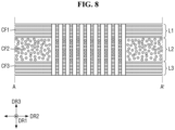
- FIG. 8 is a cross-sectional view of an example of the panel support member 700 taken along line A-A' of FIG. 7 .
- FIG. 9 illustrates an alignment mark AK of the display panel 400 and a notch NTH of the panel support member 700 according to an embodiment.
- FIG. 10 is a detailed plan view of an example of a lattice pattern 710 of the panel support member 700 of FIG. 7 .
- the panel support member 700 may be a polymer including carbon fibers or glass fibers and a resin.
- the resin may be epoxy, polyester, polyamide, polycarbonate, polypropylene, polybutylene, or vinyl ester.
- the resin may be epoxy, polyester, polyamide, or vinyl ester.
- the panel support member 700 may include a first layer L1, a second layer L2, and a third layer L3 as illustrated in FIG. 8 .
- the first layer L1 may be a prepreg including a first fiber yarn CF1 extending in the second direction DR2.
- the second layer L2 may be a prepreg including a second fiber yarn CF2 extending in the first direction DR1.
- the third layer L3 may be a prepreg including a third fiber yarn CF3 extending in the second direction DR2.
- Each of the first fiber yarn CF1, the second fiber yarn CF2, and the third fiber yarn CF3 may be a carbon fiber yarn or a glass fiber yarn.
- Each of the first fiber yarn CF1, the second fiber yarn CF2, and the third fiber yarn CF3 may have a width of about 7 to 10 ⁇ m, but embodiments of the present specification are not limited thereto.
- the first layer L1, the second layer L2, and the third layer L3 may be stacked by hot pressing or an autoclave.
- the first direction DR1 and the second direction DR2 may be orthogonal to each other.
- the first direction DR1 may be parallel to a first folding line FL1 and a second folding line FL2.
- the direction in which the second fiber yarn CF2 of the second layer L2 extends and the direction in which the folding lines FL1 and FL2 extend are the same as the first direction DR1. Therefore, the second layer L2 can be easily folded when the display device 10 is folded.
- the panel support member 700 includes only the second layer L2 having the second fiber yarn CF2, it may be bent or curved in the first direction DR1. That is, when the panel support member 700 includes only the second layer L2 having the second fiber yarn CF2, the flatness and rigidity of the panel support member 700 may be low.
- the panel support member 700 includes not only the second layer L2 but also the first layer L1 having the first fiber yarn CF1 extending in the second direction DR2 and the third layer L3 having the third fiber yarn CF3 extending in the second direction DR2, the panel support member 700 can be prevented from being curved or bent in the first direction DR1, and the rigidity of the panel support member 700 can be increased.
- a thickness of the second layer L2 may be greater than a thickness of the first layer L1 and a thickness of the third layer L3 in consideration of the folding direction of the panel support member 700.
- the thickness of the first layer L1 and the thickness of the third layer L3 may be substantially the same, but embodiments of the present specification are not limited thereto.
- the thickness of the second layer L2 may be about 120 ⁇ m
- the thickness of the first layer L1 and the thickness of the third layer L3 may be about 20 to 30 ⁇ m.
- a thickness of the panel support member 700 may be greater than a thickness of the digitizer member 900.
- the thickness of the panel support member 700 may be greater than a thickness of the display panel 400.
- the thickness of the panel support member 700 may be about 100 to 300 ⁇ m.
- the panel support member 700 includes the lattice pattern 710, a first flat part 720, and a second flat part 730.
- the lattice pattern 710 may be disposed in the folding area FDA
- the first flat part 720 may be disposed in the first non-folding area NFA1
- the second flat part 730 may be disposed in the second non-folding area NFA2.
- the lattice pattern 710 may include a plurality of slits SLT defined by a plurality of bars BAR. Each of the slits SLT may be a hole passing through the panel support member 700 in the third direction DR3.
- Each of the slits SLT may extend in the first direction DR1. That is, each of the slits SLT may be longer in the first direction DR1 than in the second direction DR2.
- the lattice pattern 710 including the slits SLT may have flexibility. That is, the lattice pattern 710 may be stretched in the second direction DR2 when the display device 10 is folded.
- a plurality of slits SLT disposed in first through eleventh columns C1 through C11 are illustrated as an example of the lattice pattern 710.
- Each of the slits SLT disposed in the first column C1 may be defined as a first slit SLT1
- each of the slits SLT disposed in the second column C2 may be defined as a second slit SLT2
- each of the slits SLT disposed in the third column C3 may be defined as a third slit SLT3.
- Each of the slits SLT disposed in the fourth column C4 may be defined as a fourth slit SLT4, each of the slits SLT disposed in the fifth column C5 may be defined as a fifth slit SLT5, and each of the slits SLT disposed in the sixth column C6 may be defined as a sixth slit SLT6.
- Each of the slits SLT disposed in the seventh column C7 may be defined as a seventh slit SLT7
- each of the slits SLT disposed in the eighth column C8 may be defined as an eighth slit SLT8, and each of the slits SLT disposed in the ninth column C9 may be defined as a ninth slit SLT9.
- Each of the slits SLT disposed in the tenth column C10 may be defined as a tenth slit SLT 10
- each of the slits SLT disposed in the eleventh column C11 may be defined as an eleventh slit SLT11.
- the bars BAR may include first through tenth vertical bars VBAR1 through VBAR10 and first through eleventh horizontal bars HBAR1 through HBAR11.
- the first vertical bar VBAR1 may be disposed between the first slits SLT1 and the second slits SLT2
- the second vertical bar VBAR2 may be disposed between the second slits SLT2 and the third slits SLT3
- the third vertical bar VBAR3 may be disposed between the third slits SLT3 and the fourth slits SLT4
- the fourth vertical bar VBAR4 may be disposed between the fourth slits SLT4 and the fifth slits SLT5
- the fifth vertical bar VBAR5 may be disposed between the fifth slits SLT5 and the sixth slits SLT6.
- the sixth vertical bar VBAR6 may be disposed between the sixth slits SLT6 and the seventh slits SLT7
- the seventh vertical bar VBAR7 may be disposed between the seventh slits SLT7 and the eighth slits SLT8
- the eighth vertical bar VBAR8 may be disposed between the eighth slits SLT8 and the ninth slits SLT9
- the tenth vertical bar VBAR10 may be disposed between the tenth slits SLT10 and the eleventh slits SLT11
- an eleventh vertical bar VBAR11 may be disposed between the eleventh slits SLT11 and twelfth slits SLT12.
- the first horizontal bar HBAR1 may be disposed between the first slits SLT1 neighboring each other in the first direction DR1
- the second horizontal bar HBAR2 may be disposed between the second slits SL2 neighboring each other in the first direction DR1
- the third horizontal bar HBAR3 may be disposed between the third slits SLT3 neighboring each other in the first direction DR1.
- the fourth horizontal bar HBAR4 may be disposed between the fourth slits SLT4 neighboring each other in the first direction DR1
- the fifth horizontal bar HBAR5 may be disposed between the fifth slits SLT5 neighboring each other in the first direction DR1
- the sixth horizontal bar HBAR6 may be disposed between the sixth slits SLT6 neighboring each other in the first direction DR1.
- the seventh horizontal bar HBAR7 may be disposed between the seventh slits SLT7 neighboring each other in the first direction DR1
- the eighth horizontal bar HBAR8 may be disposed between the eighth slits SLT8 neighboring each other in the first direction DR1
- the ninth horizontal bar HBAR9 may be disposed between the ninth slits SLT9 neighboring each other in the first direction DR1
- the tenth horizontal bar HBAR10 may be disposed between the tenth slits SLT10 neighboring each other in the first direction DR1.
- the first slits SLT1, the second slits SLT2, the third slits SLT3, and the fourth slits SLT4 may be sequentially disposed in the second direction DR2.
- the first slits SLT2 and the fourth slits SLT4 among the first slits SLT1, the second slits SLT2, the third slits SLT3, and the fourth slits SLT4 sequentially disposed in the second direction DR2 may be shifted in the first direction DR1 compared with the first slits SLT1 and the third slits SLT3.
- a lower half of the first slits SLT1, an upper half of the second slits SLT2, a lower half of the third slits SLT3, and an upper half of the fourth slits SLT4 may overlap each other in the first direction DR1.
- an upper half of the first slits SLT1, a lower half of the second slits SLT2, an upper half of the third slits SLT3, and a lower half of the fourth slits SLT4 may overlap each other in the first direction DR1.
- first horizontal bars HBAR1 and the third horizontal bars HBAR3 may be disposed side by side in the second direction DR2, and the second horizontal bars HBAR2 and the fourth horizontal bars HBAR4 may be disposed side by side in the second direction DR2.
- second horizontal bars HBAR2 may be disposed between the first slits SLT1 and the third slits SLT3
- third horizontal bars HBAR3 may be disposed between the second slits SLT2 and the fourth slits SLT4.
- a front surface of each of the first flat part 720 and the second flat part 730 may be formed to be flat.
- One or more notches NTH may be disposed on each of side surfaces of the first flat part 720 and the second flat part 730.
- the notches NTH may be formed in the shape of grooves or ditches extending in the third direction DR3.
- Each of the notches NTH may be a recessed part of the side surface of the first flat part 720 or the second flat part 730.
- a notch NTH may overlap an alignment mark AK disposed on the front surface of the display panel 400 in the third direction DR3 as illustrated in FIG. 9 . Accordingly, an alignment camera AC, the notch NTH, and the alignment mark AK may be aligned in the third direction DR3. Therefore, the alignment mark AK disposed on the rear surface of the display panel 400 may be photographed by the alignment camera AC through the notch NTH. Therefore, the display panel 400 may be aligned with another element (e.g., the digitizer member 900) by aligning the alignment mark AK of the display panel 400 with an alignment mark of another element (e.g., the digitizer member 900) through the alignment camera AC.
- another element e.g., the digitizer member 900
- the through hole STH passing through the panel support member 700 may be disposed in the first flat part 720.
- the through hole STH may be disposed adjacent to an edge of the first flat part 720.
- FIG. 11 is a flowchart illustrating a method of manufacturing a display device according to an embodiment. The method of manufacturing the display device according to the embodiment will now be described in detail with reference to FIG. 11 .
- a panel support member 700 having edges suitable for a display panel 400 of a display device 10 is formed by machining an unmachined panel support member 700_1 using a laser of a laser device.
- the panel support member 700 may include notches NTH for exposing alignment marks AK of the display panel 400 in the third direction DR3 without covering the alignment marks AK (operation S100 of FIG. 11 ).
- the laser device outputs a laser along a first machining line PL1 and then outputs a laser along a second machining line PL2. Then, the laser device outputs a laser along a third machining line PL3 and then outputs a laser along a fourth machining line PL4. The laser device outputs a laser several to tens of times along the first through fourth machining lines PL1 through PL4, thereby machining the edges of the panel support member 700. The number of times that the laser device outputs a laser may vary according to the energy of the laser.
- the first machining line PL1 may be a line for forming a first side (e.g., a left side) of the panel support member 700 in plan view. A left surface of the panel support member 700 may be formed by the first machining line PL1.
- the first machining line PL1 may extend in the first direction DR1 except for the notches NTH.
- the second machining line PL2 may be a line for forming a second side (e.g., an upper side) of the panel support member 700 in plan view.
- An upper surface of the panel support member 700 may be formed by the second machining line PL2.
- the second machining line PL2 may extend in the second direction DR2 except for the notches NTH.
- the third machining line PL3 may be a line for forming a third side (e.g., a right side) of the panel support member 700 in plan view. A right surface of the panel support member 700 may be formed by the third machining line PL3.
- the third machining line PL3 may extend in the first direction DR1 except for the notches NTH.
- the fourth machining line PL4 may be a line for forming a fourth side (e.g., a lower side) of the panel support member 700 in plan view. A lower surface of the panel support member 700 may be formed by the fourth machining line PL4. The fourth machining line PL4 may extend in the second direction DR2 except for the notches NTH.
- the laser device may output a laser several to tens of times along a fifth machining line PL5, thereby machining a through hole STH of the panel support member 700.
- the fifth machining line PL5 may have substantially the same planar shape as the through hole STH.
- a third fiber yarn CF3 of a third layer L3 of the panel support member 700 extends in the first direction DR1, and the first machining line PL1 also extends in the first direction DR1.
- the extending direction of the first machining line PL1 and the extending direction of the third fiber yarn CF3 may not completely coincide with each other. Therefore, when the panel support member 700 is machined or cut along the first machining line PL1 by using a laser, the third fiber yarn CF3 may not be properly cut, and a cut part of the third fiber yarn CF3 may remain in the form of a byproduct BURR.
- the third fiber yarn CF3 removed by cutting the panel support member 700_1 along the first machining line PL1 in area A is shown in dotted lines for ease of description.
- a first fiber yarn CF1 of a first layer L1 of the panel support member 700 may also extend in the first direction DR1.
- the extending direction of the first machining line PL1 and the extending direction of the first fiber yarn CF1 may not completely coincide with each other. Therefore, when the panel support member 700 is machined or cut along the first machining line PL1 by using a laser, the first fiber yarn CF1 may not be properly cut, and a cut part of the first fiber yarn CF 1 may remain in the form of a byproduct BURR.
- a cut part of the first fiber yarn CF1 or the third fiber yarn CF3 of the panel support member 700 may remain in the form of a byproduct BURR.
- a second fiber yarn CF2 of a second layer L2 of the panel support member 700 extends in the second direction DR2, and the second machining line PL2 also extends in the second direction DR2.
- the extending direction of the second machining line PL2 and the extending direction of the second fiber yarn CF2 may not completely coincide with each other. Therefore, when the panel support member 700 is machined or cut along the second machining line PL2 by using a laser, the second fiber yarn CF2 may not be properly cut, and a cut part of the second fiber yarn CF2 may remain in the form of a byproduct BURR.
- the second fiber yarn CF2 removed by cutting the panel support member 700_1 along the second machining line PL2 in area B is shown in dotted lines for ease of description.
- a cut part of the second fiber yarn CF2 of the panel support member 700 may remain in the form of a byproduct BURR.
- a cut part of the first fiber yarn CF1 or the third fiber yarn CF3 may remain as the byproduct BURR in area A, and a cut part of the second fiber yarn CF2 may remain as the byproduct BURR in area B.
- the laser device outputs a laser of high energy to reduce the machining time for edge machining of the panel support member 700
- high thermal energy may be generated on a surface cut by the laser.
- the thermal energy may cause a resin holding the fiber yarns CF1 through CF3 in the panel support member 700 to fall off.
- a cut part of the first fiber yarn CF1, the second fiber yarn CF2, or the third fiber yarn CF3 may protrude outward from the cut surface of the panel support member 700 and remain as the byproduct BURR.
- the alignment mark AK when an alignment mark AK of the display panel 400 is photographed using an alignment camera AC as illustrated in FIG. 9 , the alignment mark AK may not be properly recognized due to the byproduct BURR.
- the machining time may be increased by an alarm generated in a process of monitoring the side surfaces of the panel support member 700. Therefore, the energy of a laser output from the laser device needs to be lowered to prevent a cut part of the first fiber yarn CF1, the second fiber yarn CF2, or the third fiber yarn CF3 from remaining as the byproduct BURR on the side surfaces of the panel support member 700.
- a laser used to machine the panel support member 700 may be an ultraviolet laser or an infrared laser.
- the ultraviolet laser refers to a laser that emits light having energy of an ultraviolet wavelength
- the infrared laser refers to a laser that emits light having energy of an infrared wavelength.
- the ultraviolet wavelength may be about 10 to 400 nm
- the infrared wavelength may be about 750 nm to 1 ⁇ m.
- the energy of the laser may be adjusted by a scan speed of the laser, a pulse period of the laser, a pulse repetition rate of the laser, and power of the laser.
- the inventors of the present disclosure have calculated, through repeated experiments, the scan speed of the laser, the pulse period of the laser, the pulse repetition rate of the laser, and the power of the laser for preventing a cut part of the first fiber yarn CF1, the second fiber yarn CF2 or the third fiber yarn CF3 from remaining as the byproduct BURR on the side surfaces of the panel support member 700 as shown in Table 1.
- the wavelength band of the laser may be divided into an ultraviolet wavelength band and an infrared wavelength band.
- the scan speed of the laser, the pulse period of the laser, the pulse repetition rate of the laser, and the power of the laser may vary according to the wavelength band of the laser.
- the scan speed of the laser, the pulse repetition rate of the laser, and the power of the laser may vary according to the pulse period of the laser.
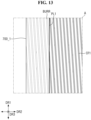
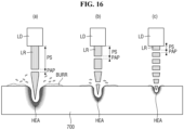
- the pulse period of the laser refers to a period in which the laser is output when the laser is output in a periodic waveform, like a predetermined pulse. As illustrated in FIG. 16 , a pause period PAP in which the laser is not output may be disposed between pulse periods PS.
- the pulse period may be in units of nanoseconds (ns) or in units of picoseconds (ps) or femtoseconds (fs).
- the pulse period of the laser may be in units of picoseconds (ps) or femtoseconds (fs).
- a nanosecond unit refers to several to hundreds of nanoseconds
- a picosecond unit refers to several to hundreds of picoseconds
- a femtosecond unit refers to several to hundreds of femtoseconds.
- the scan speed of the laser refers to the speed at which the laser device outputting the laser moves in a machining direction. That is, the scan speed of the laser may refer to the speed at which the laser device emits the laser while moving along the first through fourth machining lines PL1 through PL4.
- the pulse repetition rate of the laser refers to the number of pulses transmitted from the laser device per second.
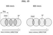
- spots SP of the laser may be defined according to the pulse period of the laser.
- Each of the spots SP of the laser may have a circular planar shape.
- a diameter of each of the spots SP of the laser may be about 20 ⁇ m, but embodiments of the present specification are not limited thereto.
- an overlap rate OVA1 of the laser spots SP when the scan speed of the laser is 300 mm/s may be greater than an overlap rate OVA2 of the laser spots SP when the scan speed of the laser is 800 mm/s.
- the overlap rate of the laser spots SP may increase as the pulse repetition rate of the laser increases. Since the overlap area between the spots SP of the laser increases as the overlap rate of the spots SP of the laser increases, the energy of the laser may increase. Accordingly, higher thermal energy may be generated on a surface cut by the laser. Therefore, when the overlap rate of the laser spots SP is reduced, the energy of the laser can be reduced. Accordingly, when the scan speed of the laser is increased or when the pulse repetition rate of the laser is reduced, the energy of the laser can be reduced.
- FIG. 16A illustrates a laser device LD that outputs a laser LR during a pulse period PS having a unit of nanoseconds (ns).
- FIG. 16B illustrates a laser device LD that outputs a laser LR during a pulse period PS having a unit of picoseconds (ps).
- FIG. 16C illustrates a laser device LD that outputs a laser LR during a pulse period PS having a unit of femtoseconds (fs).
- the laser LR having higher energy is output. Accordingly, higher thermal energy may be applied to the panel support member 700 by the laser LR. Therefore, a thermal energy area HEA applied to the panel support member 700 by the laser LR may be wide. Hence, as the pulse period PS of the laser LR is reduced, the energy of the laser LR may be reduced.
- the scan speed of the laser LR may be increased or the pulse repetition rate of the laser LR may be reduced compared with when the pulse period PS of the laser LR is in units of picoseconds (ps) or femtoseconds (fs).
- the scan speed of the laser may be 800 mm/s or less
- the pulse repetition rate of the laser may be 200 kHz or less
- the power of the laser may be 13 W or less.
- the scan speed of the laser may be 5000 mm/s or less, the pulse repetition rate of the laser may be 3000 kHz or less, and the power of the laser may be 50 W or less.
- the scan speed of the laser may be 1000 mm/s or less, the pulse repetition rate of the laser may be 2000 kHz or less, and the power of the laser may be 20 W or less.
- a lattice pattern LP is machined in a folding area FDA of the panel support member 700 by using a laser of the laser device.
- the lattice pattern LP may include a plurality of slits SLT defined by a plurality of bars BAR (operation S200 of FIG. 11 ).
- first through eleventh slits SLT1 through SLT11 disposed in the second direction DR2 may be sequentially machined using a laser.
- a first slit SLT1 may be machined using a laser, and then a second slit SLT2 neighboring the first slit SLT1 in the second direction DR2 may be machined.
- a third slit SLT3 neighboring the second slit SLT2 in the second direction DR2 may be machined.
- thermal energy due to the laser may be accumulated in an area HA of a first vertical bar VBAR1 disposed between the first slit SLT1 and the second slit SLT2.
- thermal energy due to the laser may be accumulated in an area HA of a second vertical bar VBAR2 disposed between the second slit SLT2 and the third slit SLT3.
- thermal energy due to a laser may also be accumulated in an area HA of a third vertical bar VBAR3 disposed between the third slit SLT3 and a fourth slit SLT4, in an area HA of a fourth vertical bar VBAR4 disposed between the fourth slit SLT4 and a fifth slit SLT5, in an area HA of a fifth vertical bar VBAR5 disposed between the fifth slit SLT5 and a sixth slit SLT6, and in an area HA of a sixth vertical bar VBAR6 disposed between the sixth slit SLT6 and a seventh slit SLT7.
- thermal energy due to a laser may be accumulated in an area HA of a seventh vertical bar VBAR7 disposed between the seventh slit SLT7 and an eighth slit SLT8, in an area HA of an eighth vertical bar VBAR8 disposed between the eighth slit SLT8 and a ninth slit SLT9, in an area HA of a ninth vertical bar VBAR9 disposed between the ninth slit SLT9 and a tenth slit SLT10, and in an area HA of a tenth vertical bar VBAR10 disposed between the tenth slit SLT1 and an eleventh slit SLT11.
- FIGS. 18A and 18B are plan views of a lattice pattern
- FIGS. 18C and 18D are side views or cross-sectional views of the lattice pattern.
- a resin holding the fiber yarns CF1 through CF3 may fall off, or cracks may be created in the resin as illustrated in FIG. 18 . Therefore, a cut part of the first fiber yarn CF1, the second fiber yarn CF2, or the third fiber yarn CF3 may protrude outward and remain as the byproduct BURR.
- any one of the first slits SLT1 may be machined first, and then a third slit SLT3, a fifth slit SLT5, a seventh slit SLT7, a ninth slit SLT9, and an eleventh slit SLT11 overlapping the first slit SLT1 machined for the first time in the second direction DR2 may be sequentially machined (see 1 through 6 of FIG. 19 ).
- a first slit SLT1 may be machined
- a second slit SLT2 may be skipped
- a third slit SLT3 may be machined
- a fourth slit SLT4 may be skipped
- a fifth slit SLT5 may be machined
- a sixth slit SLT6 may be skipped
- a seventh slit SLT7 may be machined
- an eighth slit SLT8 may be skipped
- a ninth slit SLT9 may be machined
- a tenth slit SLT10 may be skipped
- an eleventh slit SLT11 may be machined.
- a slit SLT2/SLT4/SLT6/SLT8/SLT10 in an even column may be disposed between neighboring slits among the slits SLT1, SLT3, SLT6, SLT7, SLT9, and SLT11 in odd columns machined for the first through sixth times. Therefore, thermal energy due to a laser may not be accumulated in any one of the bars BAR.
- the eleventh slit SLT11 may be machined for the sixth time.
- another eleventh slit SLT11 overlapping the eleventh slit SLT11 in the first direction DR1 may be machined for the seventh time.
- the eleventh slit SLT11 machined for the sixth time and the eleventh slit SLT11 machined for the seventh time may not neighbor each other. That is, an eleventh slit SLT11 neighboring the eleventh slit SLT11 machined for the sixth time in the first direction DR1 may be skipped, and the eleventh slit SLT11 neighboring the skipped eleventh slit SLT11 in the first direction DR1 may be machined.
- a ninth slit SLT9, a seventh slit SLT7, a fifth slit SLT5, a third slit SLT3, and a first slit SLT1 overlapping the eleventh slit SLT11 machined for the seventh time in the second direction DR2 may be sequentially machined (see 7 through 12 of FIG. 19 ).
- a slit SLT2/SLT4/SLT6/SLT8/SLT10 in an even column may be disposed between neighboring slits among the slits SLT1, SLT3, SLT6, SLT7, SLT9, and SLT11 in odd columns machined for the seventh through twelfth times. Therefore, thermal energy due to a laser may not be accumulated in any one of the bars BAR.
- a second slit SLT2 neighboring the first slit SLT1 machined for the first time in the second direction DR2 may be machined for the thirteenth time.
- a fourth slit SLT4, a sixth slit SLT6, an eighth slit SLT8, and a tenth slit SLT10 overlapping the second slit SLT2 machined for the thirteenth time in the second direction DR2 may be sequentially machined (see 13 through ⁇ ,17 of FIG. 19 ).
- a slit SLT3/SLT5/SLT7/SLT9 in an odd column may be disposed between neighboring slits among the slits SLT2, SLT4, SLT6, SLT8, and SLT10 in even columns formed for the thirteenth through seventeenth times. Therefore, thermal energy due to a laser may not be accumulated in any one of the bars BAR.
- another tenth slit SLT10 overlapping the tenth slit SLT10 machined for the seventeenth time in the second direction DR2 may be machined for the eighteenth time.
- the tenth slit SLT10 machined for the seventeenth time and the tenth slit SLT10 machined for the eighteenth time may not neighbor each other.
- the tenth slit SLT10 machined for the eighteenth time may neighbor the eleventh slit SLT11 machined for the seventh time in the first direction DR1.
- an eighth slit SLT8, a sixth slit SLT6, a fourth slit SLT4, and a second slit SLT2 overlapping the tenth slit SLT10 machined for the eighteenth time in the second direction DR2 may be sequentially machined (see ⁇ ,18 through ⁇ ,22 of FIG. 19 ).
- a slit SLT3/SLT5/SLT7/SLT9 in an odd column may be disposed between neighboring slits among the slits SLT2, SLT4, SLT6, SLT8, and SLT10 in even columns machined for the eighteenth through twenty-second times. Therefore, thermal energy due to a laser may not be accumulated in any one of the bars BAR.
- a first slit SLT1 disposed between the first slit SLT1 machined for the first time and the first slit SLT1 machined for the twelfth time may be machined for the twenty-third time.
- a third slit SLT3, a fifth slit SLT5, a seventh slit SLT7, a ninth slit SLT9, and an eleventh slit SLT11 overlapping the first slit SLT1 machined for the twenty-third time in the second direction DR2 may be sequentially machined (see ⁇ ,23 through o,28 of FIG. 19 ).
- a slit SLT2/SLT4/SLT6/SLT8/SLT10 in an even column may be disposed between neighboring slits among the slits SLT1, SLT3, SLT5, SLT6, SLT7, SLT9, and SLT11 in odd columns machined for the twenty-third through twenty-eighth times. Therefore, thermal energy due to a laser may not be accumulated in any one of the bars BAR.
- a tenth slit SLT 10 overlapping the eleventh slit SLT 11 machined for the sixth time in the second direction DR2 may be machined for the twenty-ninth time.
- an eighth slit SLT8, a sixth slit SLT6, a fourth slit SLT4, and a second slit SLT2 overlapping the tenth slit SLT10 machined for the twenty-ninth time in the second direction DR2 may be sequentially machined (see ⁇ ,29 through o,33 of FIG. 19 ).
- a slit SLT3/SLT5/SLT7/SLT9 in an odd column may be disposed between neighboring slits among the slits SLT2, SLT4, SLT6, SLT8, and SLT10 in even columns machined for the twenty-ninth through thirty-third times. Therefore, thermal energy due to a laser may not be accumulated in any one of the bars BAR.
- a second slit SLT2 disposed between the second slit SLT2 machined for the thirteenth time and the second slit SLT2 machined for the twenty-second time may be machined for the thirty-fourth time.
- a fourth slit SLT4, a sixth slit SLT6, an eighth slit SLT8, and a tenth slit SLT10 overlapping the second slit SLT2 machined for the thirty-fourth time in the second direction DR2 may be sequentially machined (see o,34 through o,38 of FIG. 19 ).
- a slit SLT3/SLT5/SLT7/SLT9 in an odd column may be disposed between neighboring slits among the slits SLT2, SLT4, SLT6, SLT8, and SLT10 in even columns machined for the thirty-fourth through thirty-eighth times. Therefore, thermal energy due to a laser may not be accumulated in any one of the bars BAR.
- FIG. 20A is a plan view of a lattice pattern
- FIG. 20B is a side view or cross-sectional view of the lattice pattern. Since there is no area in which thermal energy due to a laser is accumulated, the resin holding the fiber yarns CF1 through CF3 does not fall off, or cracks are not created in the resin. Therefore, it is possible to prevent a cut part of the first fiber yarn CF1, the second fiber yarn CF2, or the third fiber yarn CF3 from protruding outward and remaining as the byproduct BURR.
- an under-panel member 600 is attached onto a surface of the completed panel support member 700, and a digitizer member 900 is attached onto the other surface of the panel support member 700 (operation S300 of FIG. 11 ).
- a surface of the panel support member 700 may be a front surface, and the other surface may be a rear surface.
- a separate adhesive member may be disposed between the under-panel member 600 and the panel support member 700.
- the separate adhesive member may be a pressure sensitive adhesive.
- a first digitizer member 910 and a second digitizer member 920 of the digitizer member 900 may be attached to the rear surface of the panel support member 700 by a second adhesive member 800.
- the second adhesive member 800 may be a pressure sensitive adhesive.
- the first digitizer member 910 and the second digitizer member 920 may not be disposed in the folding area FDA to reduce folding stress of the display device 10.
- the first digitizer member 910 may be disposed in a first non-folding area NFA1, and the second digitizer member 920 may be disposed in a second non-folding area NFA2.
- a first metal support member 1010 of a metal support member 1000 may be disposed on a rear surface of the first digitizer member 910, and a second metal support member 1020 may be disposed on a rear surface of the second digitizer member 920.
- a first buffer member 1110 of a buffer member 1100 may be disposed on a rear surface of the first metal support member 1010, and a second buffer member 1120 may be disposed on a rear surface of the second metal support member 1020.
- a third adhesive member 1200 may be disposed on the rear surface of the first metal support member 1010 and the rear surface of the second metal support member 1020.
- the third adhesive member 1200 may be disposed on edges of the first metal support member 1010 and edges of the second metal support member 1020 and may surround the first buffer member 1110 and the second buffer member 1120.
- the third adhesive member 1200 may be a waterproof tape or a waterproof member for attaching the rear surface of the first metal support member 1010 to a front surface of a frame disposed on a rear surface of the buffer member 1100.
- a window member 200 is attached to a front surface of the display panel 400 (operation S400 of FIG. 11 ).
- the window member 200 may be attached onto the front surface of the display panel 400 by a first adhesive member 300.
- the first adhesive member 300 may be a transparent adhesive film or a transparent adhesive resin.
- an upper protection member 100 may be disposed on a front surface of the window member 200.
- the under-panel member 600 is attached to a rear surface of the display panel 400 (operation S500 of FIG. 11 ).
- a panel protection member 500 may be disposed on the rear surface of the display panel 400.
- the under-panel member 600 may be attached to the rear surface of the display panel 400.
Landscapes
- Engineering & Computer Science (AREA)
- Theoretical Computer Science (AREA)
- Computer Hardware Design (AREA)
- Physics & Mathematics (AREA)
- General Physics & Mathematics (AREA)
- General Engineering & Computer Science (AREA)
- Human Computer Interaction (AREA)
- Mathematical Physics (AREA)
- Optics & Photonics (AREA)
- Life Sciences & Earth Sciences (AREA)
- Chemical & Material Sciences (AREA)
- Inorganic Chemistry (AREA)
- Sustainable Development (AREA)
- Devices For Indicating Variable Information By Combining Individual Elements (AREA)
- Electroluminescent Light Sources (AREA)
Abstract
Description
- Embodiments of the invention relate to a foldable display device and a method of manufacturing the same.
- As the information society develops, demands for display devices for displaying imag es are increasing in various forms. For example, display devices are being applied to vari ous electronic devices such as smartphones, digital cameras, notebook computers, navigation devices, and smart televisions.
- In order to increase portability of a display device while providing a wide display screen, a bendable display device in which a display area can be bent or a foldable display device in which a display area can be folded have been released recently.
- In addition, a display device supports a touch input using a user's body part (e.g., a finger) and a touch input using an electronic pen (e.g., a stylus pen). Since the display device uses the touch input using the electronic pen, it can sense a touch input more precisely than when using only the touch input using the user's body part. In this case, if a metal support member is used to support a display panel of the foldable display device, the sensitivity of the touch input using the electronic pen may be reduced due to the metal support member.
- Aspects of the present invention are to provide a foldable display device including a panel support member which can support a display panel while not reducing the sensitivity of a touch input using an electronic pen.
- Aspects of the present invention are to provide a method of manufacturing a foldable display device including a panel support member which can support a display panel while not reducing the sensitivity of a touch input using an electronic pen.
- However, aspects of the present invention are not restricted to the one set forth herein. The above and other aspects of the present invention will become more apparent to one of ordinary skill in the art to which the present invention pertains by referencing the detailed description of the present invention given below.
- An embodiment of the invention provides a foldable display device including a display panel which comprises a folding area, a first non-folding area disposed on a side of the folding area, and a second non-folding area disposed on the other side of the folding area, and a panel support member which is disposed on a surface of the display panel and includes a plurality of slits extending in a first direction. The panel support member includes a first layer which has a first fiber yarn extending in a second direction intersecting the first direction, a second layer which has a second fiber yarn extending in the first direction, and a third layer which has a third fiber yarn extending in the second direction.
- In an embodiment, a thickness of the second layer may be greater than a thickness of the first layer and a thickness of the third layer.
- In an embodiment, the second direction may be parallel to a first folding line corresponding to a boundary between the folding area and the first non-folding area and a second folding line corresponding to a boundary between the folding area and the second non-folding area.
- In an embodiment, the slits may be disposed in the folding area.
- In an embodiment, the slits may include first slits disposed in a first column, second slits disposed in a second column and third slits disposed in a third column, and the second slits are shifted in the first direction compared with the first slits and the third slits.
- In an embodiment, a lower half of any one of the first slits, an upper half of any one of the second slits, and a lower half of any one of the third slits may overlap each other in the second direction.
- An embodiment of the invention provides a foldable display device including a display panel which comprises an alignment mark, and a panel support member which is disposed on a surface of the display panel and comprises a notch extending in a thickness direction of the display panel. The panel support member includes a first layer which has a first fiber yarn extending in a second direction intersecting a first direction, a second layer which has a second fiber yarn extending in the first direction, and a third layer which has a third fiber yarn extending in the second direction. The alignment mark may overlap the notch in the thickness direction of the display panel.
- In an embodiment, the notch may be shaped like a groove or a ditch recessed from a side surface of the panel support member.
- In an embodiment, the foldable display device may further include an optical device which senses light. The display panel may include a light transmitting area which overlaps the optical device in the thickness direction of the display panel, and the panel support member may include a through hole which overlaps the light transmitting area in the thickness direction of the display panel.
- In an embodiment, the area of the light transmitting area may be larger than the area of the through hole.
- An embodiment of the invention provides a method of manufacturing a foldable display device including machining edges of a panel support member by using a laser, forming a lattice pattern in a folding area of the panel support member by using the laser, attaching a digitizer member onto a surface of the panel support member, and attaching the panel support member onto a surface of a display panel.
- In an embodiment, a pulse period of the laser may be several to hundreds of nanoseconds, several to hundreds of picoseconds, or several to hundreds of femtoseconds.
- In an embodiment, when the laser is an ultraviolet laser and the pulse period of the laser is several to hundreds of nanoseconds, a scan speed of the laser may be 800 mm/s or less, a pulse repetition rate of the laser may be 200 kHz or less, and power of the laser may be 13 W or less.
- In an embodiment, when the laser is an ultraviolet laser and the pulse period of the laser may be several to hundreds of picoseconds or several to hundreds of femtoseconds, the scan speed of the laser may be 5000 mm/s or less, the pulse repetition rate of the laser may be 3000 kHz or less, and the power of the laser may be 50 W or less.
- In an embodiment, wherein when the laser is an infrared laser and the pulse period of the laser is several to hundreds of picoseconds or several to hundreds of femtoseconds, the scan speed of the laser may be 1000 mm/s or less, the pulse repetition rate of the laser may be 2000 kHz or less, and the power of the laser may be 20 W or less.
- In an embodiment, the method may further include forming a through hole passing through the panel support member by using the laser.
- In an embodiment, wherein in the machining of the edges of the panel support member by using the laser, at least one notch disposed on a side surface of the panel support member may be machined.
- In an embodiment, the lattice pattern may include a plurality of slits which are defined by a plurality of bars and extend in a first direction.
- In an embodiment, the slits comprise a first slit, a second slit, and a third slit disposed in a second direction intersecting the first direction, and the forming of the lattice pattern in the folding area of the panel support member by using the laser may include machining the first slit, skipping the second slit, and machining the third slit.
- In an embodiment, the slits may include a plurality of first slits disposed in the first direction, and the forming of the lattice pattern in the folding area of the panel support member by using the laser may include machining any one of the first slits, skipping a first slit neighboring the machined first slit in the first direction, and machining a first slit neighboring the skipped first slit in the first direction.
- Other features and embodiments may be apparent from the following detailed description, and the drawings.
- In embodiments of a display device and a method of manufacturing the same according to the invention, a panel support member is included. The panel support member is disposed on a rear surface of a display panel and is a rigid member that is not easily changed in shape or volume by external pressure. Since the panel support member is made of a polymer including carbon fibers or glass fibers, a magnetic field or electromagnetic signal of a digitizer member can pass through the panel support member. Therefore, the panel support member can stably support the display panel while not reducing the touch sensitivity of the digitizer member.
- In embodiments of a display device and a method of manufacturing the same according to the invention, the energy of a laser applied to a panel support member can be reduced by adjusting a pulse period of the laser, a scan speed of the laser, a pulse repetition rate of the laser, and power of the laser. Therefore, since thermal energy generated on a cut surface of the panel support member can be reduced, it is possible to prevent a resin holding fiber yarn from falling off or cracking due to the thermal energy. Accordingly, it is possible to prevent a cut part of the fiber yarn from remaining as a byproduct on the cut surface of the panel support member.
- In embodiments of a display device and a method of manufacturing the same according to the invention, when a lattice pattern is formed in a folding area of a panel support member, the machining order of slits may be determined such that the slits neighboring each other in a first direction and a second direction are not successively machined. Therefore, an area in which thermal energy due to a laser is accumulated can be removed from a plurality of bars that define the slits. Hence, it is possible to prevent a resin holding fiber yarn from falling off or from cracking due to the thermal energy. Accordingly, it is possible to prevent a cut part of the fiber yarn from remaining as a byproduct on a cut surface of the panel support member.
- However, the effects of the present disclosure are not limited to the aforementioned effects, and various other effects are included in the present disclosure.
-
-
FIGS. 1A and1B are perspective views of a display device according to an embodiment. -
FIGS. 2A and2B are perspective views of a display device according to an embodiment. -
FIG. 3 is an exploded perspective view of a display device according to an embodiment. -
FIG. 4 is a side view of the display device according to an embodiment. -
FIG. 5 is a detailed cross-sectional view of an example of a display panel ofFIGS. 3 and4 . -
FIG. 6 is a perspective view of an example of a panel support member ofFIGS. 3 and4 . -
FIG. 7 is a plan view of an example of the panel support member ofFIGS. 3 and4 . -
FIG. 8 is a cross-sectional view of an example of the panel support member taken along line A-A' ofFIG. 7 . -
FIG. 9 illustrates an alignment mark of the display panel and a notch of the panel support member according to an embodiment. -
FIG. 10 is a detailed plan view of an example of a lattice pattern of the panel support member ofFIG. 7 . -
FIG. 11 is a flowchart illustrating a method of manufacturing a display device according to an embodiment. -
FIG. 12 illustrates an edge machining order of a panel support member according to an embodiment. -
FIG. 13 is an exemplary view illustrating a byproduct according to an extending direction of fiber yarn of a third layer of the panel support member and a laser movement direction in area A ofFIG. 12 . -
FIG. 14 is an exemplary view illustrating a byproduct according to an extending direction of fiber yarn of a second layer of the panel support member and a laser movement direction in area B ofFIG. 12 . -
FIG. 15 is an exemplary view illustrating laser spots according to a scan speed of a laser. -
FIG. 16 is an exemplary view illustrating a thermal energy area generated by a laser according to a pulse period of the laser. -
FIG. 17 illustrates a machining order of a lattice pattern of a panel support member according to an embodiment. -
FIG. 18 shows images of a plane and a side surface of a bar of the lattice pattern of the panel support member according to an embodiment. -
FIG. 19 is a plan view illustrating a machining order of a lattice pattern of a panel support member according to an embodiment. -
FIG. 20 shows images of a plane and a side surface of a bar of the lattice pattern of the panel support member according to another embodiment. - Advantages and features of the present disclosure and methods for accomplishing these advantages and features will become apparent from exemplary embodiments to be described later in detail with reference to the accompanying drawings. However, the present disclosure is not limited to exemplary embodiments disclosed below, and may be implemented in various different forms, these exemplary embodiments will be provided only in order to make the present disclosure complete and allow one of ordinary skill in the art to which the present disclosure pertains to completely recognize the scope of the present disclosure, and the present disclosure will be defined by the scope of the claims.
- The phrase "one element or layer 'on' another element or layer" includes both of a case where one element or layer is disposed immediately above another element or layer and a case where one element or layer is disposed above another element or layer with the other layer or element interposed therebetween. Throughout the specification, the same components will be denoted by the same reference numerals. The shape, size, ratio, angle, number and the like shown in the drawings to illustrate the embodiments of the present disclosure are only for illustration and are not limited to the contents shown in the drawings.
- The terms "first", "second", and the like are used to describe various components, but these components are not limited by these terms. These terms are used only in order to distinguish one component from another component. Therefore, a first component mentioned below may be a second component within the technical spirit of the present disclosure.
- Features of various embodiments of the present disclosure may be coupled to or combined with each other partially or wholly and may be technically linked and operated in various ways as being easily understood by those having ordinary skill in the art. In addition, embodiments may be implemented independently or associated together.
- Hereinafter, embodiments of the invention will be described in detail with reference to the accompanying drawings.
-
FIGS. 1A and1B are perspective views of afoldable display device 10 according to an embodiment. -
FIG. 1A illustrates a first state in which thefoldable display device 10 is not folded at folding lines FL1 and FL2, andFIG. 1B illustrates a second state in which thefoldable display device 10 is folded at the folding lines FL1 and FL2. - Referring to
FIGS. 1A and1B , thefoldable display device 10 according to the embodiment is a device for displaying moving images or still images. Thefoldable display device 10 may be used as a display screen in portable electronic devices such as mobile phones, smartphones, tablet personal computers (PCs), smart watches, watch phones, mobile communication terminals, electronic notebooks, electronic books, portable multimedia players (PMPs), navigation devices and ultra-mobile PCs (UMPCs), as well as in various products such as televisions, notebook computers, monitors, billboards and the Internet of things (IoT). - In
FIGS. 1A and1B , a first direction DR1 may be a direction parallel to a side of thedisplay device 10 when seen in plan view, for example, may be a horizontal direction of thedisplay device 10. A second direction DR2 may be a direction parallel to another side in contact with the above side of thedisplay device 10 when seen in plan view, for example, may be a vertical direction of thedisplay device 10. A third direction DR3 may be a thickness direction of thedisplay device 10. - The planar shape of the
display device 10 may be a quadrangular shape such as a rectangular shape. Each corner of thedisplay device 10 may have a right-angled planar shape or a round planar shape. A front surface of thedisplay device 10 may include two short sides disposed in the first direction DR1 and two long sides disposed in the second direction DR2. - The
display device 10 includes a display area DA and a non-display area NDA. The planar shape of the display area DA may follow the shape of thedisplay device 10. For example, when thedisplay device 10 is rectangular in plan view, the display area DA may also be rectangular in plan view. - The display area DA may be an area which includes a plurality of pixels to display an image. The non-display area NDA may be an area which does not include pixels and thus does not display an image. The non-display area NDA may be disposed around the display area DA. The non-display area NDA may surround the display area DA, but embodiments of the present specification are not limited thereto. The display area DA may be partially surrounded by the non-display area NDA.
- The
display device 10 may maintain both the first state which is an unfolded state and the second state which is a folded state. Thedisplay device 10 may be folded in an in-folding manner so that parts of the display area DA face each other as illustrated inFIG. 1B . In this case, parts of the front surface of thedisplay device 10 may face each other when thedisplay device 10 is folded. Alternatively, thedisplay device 10 may be folded in an out-folding manner so that parts of a rear surface of thedisplay device 10 face each other. - The
display device 10 may include a folding area FDA, a first non-folding area NFA1, and a second non-folding area NFA2. The folding area FDA may be an area in which thedisplay device 10 is bent or folded. The first non-folding area NFA1 and the second non-folding area NFA2 may be areas in which thedisplay device 10 is not bent or folded. That is, the first non-folding area NFA1 and the second non-folding area NFA2 may be flat areas of thedisplay device 10. - The first non-folding area NFA1 may be disposed on a side, e.g., a right side of the folding area FDA. The second non-folding area NFA2 may be disposed on the other side, e.g., a left side of the folding area FDA. The folding area FDA may be an area which is defined by a first folding line FL1 and a second folding line FL2 and an area in which the
display device 10 is bent with a predetermined curvature. The first folding line FL1 may be a boundary between the folding area FDA and the first non-folding area NFA1, and the second folding line FL2 may be a boundary between the folding area FDA and the second non-folding area NFA2. - The first folding line FL1 and the second folding line FL2 may extend in the first direction DR1 as illustrated in
FIGS. 1A and1B , in which case thedisplay device 10 may be folded in the second direction DR2. Therefore, since a length of thedisplay device 10 in the second direction DR2 can be reduced by about half, it may be easy for a user to carry thedisplay device 10. - When the first folding line FL1 and the second folding line FL2 extend in the second direction DR2 as illustrated in
FIGS. 1A and1B , a length of the folding area FDA in the second direction DR2 may be greater than a length of the folding area FDA in the first direction DR1. In addition, a length of the first non-folding area NFA1 in the second direction DR2 may be greater than a length of the first non-folding area NFA1 in the first direction DR1. A length of the second non-folding area NFA2 in the second direction DR2 may be greater than a length of the second non-folding area NFA2 in the first direction DR1. - Each of the display area DA and the non-display area NDA may overlap at least one of the folding area FDA, the first non-folding area NFA1, and the second non-folding area NFA2. In
FIGS. 1A and1B , each of the display area DA and the non-display area NDA overlaps the folding area FDA, the first non-folding area NFA1, and the second non-folding area NFA2. -
FIGS. 2A and2B are perspective views of adisplay device 10 according to an embodiment.FIG. 2A is a perspective view of thedisplay device 10 according to the embodiment in an unfolded state.FIG. 2B is a perspective view of thedisplay device 10 according to the embodiment in a folded state. - The embodiment of
FIGS. 2A and2B is only different from the embodiment ofFIGS. 1A and1B in that a first folding line FL1 and a second folding line FL2 extend in the first direction DR1 and thedisplay device 10 is folded in the second direction DR2 and thus that a length of thedisplay device 10 in the second direction DR2 is reduced by about half. Therefore, inFIGS. 2A and2B , a description of elements and features identical to those of the embodiment ofFIGS. 1A and1B will be omitted. - Referring to
FIGS. 2A and2B , a first non-folding area NFA1 may be disposed on a side, e.g., a lower side of a folding area FDA. A second non-folding area NFA2 may be disposed on the other side, e.g., an upper side of the folding area FDA. When the first folding line FL1 and the second folding line FL2 extend in the first direction DR1 as illustrated inFIGS. 2A and2B , a length of the folding area FDA in the first direction DR1 may be greater than a length of the folding area FDA in the second direction DR2. -
FIG. 3 is an exploded perspective view of adisplay device 10 according to an embodiment.FIG. 4 is a side view of thedisplay device 10 according to the embodiment. - Referring to
FIGS. 3 and4 , thedisplay device 10 according to the embodiment may include anupper protection member 100, awindow member 200, a firstadhesive member 300, adisplay panel 400, apanel protection member 500, an under-panel member 600, apanel support member 700, a secondadhesive member 800, adigitizer member 900, ametal support member 1000, abuffer member 1100, and athird adhesive member 1200. - The
display panel 400 may be a panel that displays an image. Thedisplay panel 400 may be an organic light emitting display panel including an organic light emitting layer, a quantum dot light emitting display panel including a quantum dot light emitting layer, an inorganic light emitting display panel using an inorganic semiconductor element as a light emitting element, or a micro light emitting display panel using a micro light emitting diode as a light emitting element. A case where thedisplay panel 400 is an organic light emitting display panel will be mainly described below, but embodiments of the present specification are not limited thereto. - The
display panel 400 may include a light transmitting area LTA overlapping an optical device OPD in the third direction DR3. The optical device OPD may be an optical sensor that senses light, for example, a camera sensor, a proximity sensor, or an illuminance sensor. The light transmitting area LTA may be a part of a display area DA. - The light transmitting area LTA may include a transmitting area that can transmit light. Alternatively, the light transmitting area LTA may be a through hole that passes through the
display panel 400. The light transmittance of the light transmitting area LTA may be higher than the light transmittance of the display area DA excluding the light transmitting area LTA. In addition, due to the transmitting area of the light transmitting area LTA, the density or integration degree of pixels in the light transmitting area LTA may be lower than the density or integration degree of pixels in the display area DA excluding the light transmitting area LTA. For example, the number of pixels per unit area in the light transmitting area LTA may be smaller than the number of pixels per unit area in the display area DA excluding the light transmitting area LTA. Alternatively, pixels per inch (PPI) in the light transmitting area LTA may be smaller than PPI in the display area DA excluding the light transmitting area LTA. - The
window member 200 may be attached onto a front surface of thedisplay panel 400 by the firstadhesive member 300. Thewindow member 200 may be made of a transparent material, for example, may be glass or plastic. For example, thewindow member 200 may be ultra-thin glass (UTG) having a thickness of 0.1 mm or less or may be a transparent polyimide film. The firstadhesive member 300 may be a transparent adhesive film or a transparent adhesive resin. - The
upper protection member 100 may be disposed on a front surface of thewindow member 200. Theupper protection member 100 may be attached to the front surface of thewindow member 200. Theupper protection member 100 may perform at least one of scattering prevention, shock absorption, dent prevention, fingerprint prevention, and anti-glare functions of thewindow member 200. - A light blocking pattern may be formed on a rear surface of the
upper protection member 100. The light blocking pattern may be disposed on or adjacent to edges of theupper protection member 100. The light blocking pattern may include a light blocking material that can block light. For example, the light blocking pattern may be an inorganic black pigment such as carbon black, an organic block pigment, or an opaque metal material. - The
panel protection member 500 may be disposed on a rear surface of thedisplay panel 400. Thepanel protection member 500 may support thedisplay panel 400 and protect the rear surface of thedisplay panel 400. Thepanel protection member 500 may be plastic such as polyethylene terephthalate (PET) or polyimide. Although thepanel protection member 500 is disposed in a folding area FDA of thedisplay device 10 inFIGS. 3 and4 , embodiments of the present specification are not limited thereto. For example, thepanel protection member 500 may be removed from the folding area FDA of thedisplay device 10 so that thedisplay device 10 can be smoothly folded. - The under-
panel member 600 may be disposed on a rear surface of thepanel protection member 500. The under-panel member 600 may include at least one of a light blocking layer for absorbing light incident from the outside, a buffer layer for absorbing external shock, and a heat dissipating layer for efficiently dissipating the heat of thedisplay panel 400. - The light blocking layer blocks transmission of light to prevent elements disposed under the light blocking layer, for example, the
digitizer member 900 from being seen from above thedisplay panel 400. The light blocking layer may include a light absorbing material such as a black pigment or a black dye. - The buffer layer absorbs external shock to prevent the
display panel 400 from being damaged. The buffer layer may be composed of a single layer or a plurality of layers. For example, the buffer layer may be made of polymer resin such as polyurethane, polycarbonate, polypropylene or polyethylene or may be made of an elastic material such as rubber, a urethane-based material, or a sponge formed by foam molding an acrylic-based material. - The heat dissipating layer may include a first heat dissipating layer including graphite or carbon nanotubes and a second heat dissipating layer made of a metal thin film (such as copper, nickel, ferrite or silver) capable of shielding electromagnetic waves and having excellent heat conductivity.
- The
panel support member 700 may be disposed on a rear surface of the under-panel member 600. Thepanel support member 700 may be a rigid member that is not easily changed in shape or volume by external pressure. For example, thepanel support member 700 may be a polymer including carbon fibers or glass fibers. Thepanel support member 700 may include a lattice pattern disposed in the folding area FDA so that it can be easily bent in the folding area FDA. - The
panel support member 700 may include a through hole STH overlapping the optical device OPD in the third direction DR3. The through hole STH may overlap the light transmitting area LTA of thedisplay panel 400 in the third direction DR3. The area of the through hole STH may be larger than the area of the light transmitting area LTA. The optical device OPD may sense light incident from a front surface of thedisplay device 10 through the light transmitting area LTA and the through hole STH. - The
panel support member 700 will be described in detail with reference toFIGS. 6 through 11 . - The
digitizer member 900 may include afirst digitizer member 910 and asecond digitizer member 920. Thefirst digitizer member 910 and thesecond digitizer member 920 may be disposed on a rear surface of thepanel support member 700. Thefirst digitizer member 910 and thesecond digitizer member 920 may be attached to the rear surface of thepanel support member 700 by the secondadhesive member 800. The secondadhesive member 800 may be a pressure sensitive adhesive. - The
first digitizer member 910 and thesecond digitizer member 920 may not be disposed in the folding area FDA to reduce folding stress of thedisplay device 10. Thefirst digitizer member 910 may be disposed in a first non-folding area NFA1, and thesecond digitizer member 920 may be disposed in a second non-folding area NFA2. A gap between thefirst digitizer member 910 and thesecond digitizer member 920 may overlap the folding area FDA and may be smaller than a width of the folding area FDA. The width of the folding area FDA may be a length of the folding area FDA in the second direction (Y-axis direction). - The
first digitizer member 910 and thesecond digitizer member 920 may include electrode patterns for sensing approach or contact of an electronic pen such as a stylus pen that supports electromagnetic resonance (EMR). Thefirst digitizer member 910 and thesecond digitizer member 920 may sense a magnetic field or electromagnetic signal emitted from the electronic pen based on the electrode patterns and determine a point, at which the sensed magnetic field or electromagnetic signal is greatest, as touch coordinates. - Magnetic metal power may be disposed on a rear surface of the
first digitizer member 910 and a rear surface of thesecond digitizer member 920. In this case, a magnetic field or an electromagnetic signal passing through thefirst digitizer member 910 and thesecond digitizer member 920 may flow into the magnetic metal powder. Therefore, due to the magnetic metal powder, it is possible to reduce the emission of the magnetic field or electromagnetic signal of thefirst digitizer member 910 and thesecond digitizer member 920 to a rear surface of thedisplay device 10. - The
metal support member 1000 may include a firstmetal support member 1010 and a secondmetal support member 1020. The firstmetal support member 1010 may be disposed on the rear surface of thefirst digitizer member 910, and the secondmetal support member 1020 may be disposed on the rear surface of thesecond digitizer member 920. - The first
metal support member 1010 and the secondmetal support member 1020 may not be disposed in the folding area FDA to reduce folding stress of thedisplay device 10. The firstmetal support member 1010 may be disposed in the first non-folding area NFA1, and the secondmetal support member 1020 may be disposed in the second non-folding area NFA2. A gap between the firstmetal support member 1010 and the secondmetal support member 1020 may overlap the folding area FDA and may be smaller than the width of the folding area FDA. - The first
metal support member 1010 and the secondmetal support member 1020 may include a material having high rigidity to support thefirst digitizer member 910 and thesecond digitizer member 920. For example, the firstmetal support member 1010 and the secondmetal support member 1020 may include stainless steel such as SUS316. - The
buffer member 1100 may include afirst buffer member 1110 and asecond buffer member 1120. Thefirst buffer member 1110 and thesecond buffer member 1120 may absorb external shock to prevent thepanel support member 700 and thedigitizer member 900 from being damaged. Thefirst buffer member 1110 and thesecond buffer member 1120 may include an elastic material such as rubber, a urethane-based material, or a sponge formed by foam molding an acrylic-based material. - The
first buffer member 1110 may be disposed on a rear surface of the firstmetal support member 1010, and thesecond buffer member 1120 may be disposed on a rear surface of the secondmetal support member 1020. Thefirst buffer member 1110 and thesecond buffer member 1120 may not be disposed in the folding area FDA to reduce folding stress of thedisplay device 10. Thefirst buffer member 1110 may be disposed in the first non-folding area NFA1, and thesecond buffer member 1120 may be disposed in the second non-folding area NFA2. A gap between thefirst buffer member 1110 and thesecond buffer member 1120 may overlap the folding area FDA and may be smaller than the width of the folding area FDA. - The
third adhesive member 1200 may be disposed on the rear surface of the firstmetal support member 1010 and the rear surface of the secondmetal support member 1020. Thethird adhesive member 1200 may be disposed on edges of the firstmetal support member 1010 and edges of the secondmetal support member 1020. Thethird adhesive member 1200 may surround thefirst buffer member 1110 and thesecond buffer member 1120. Thethird adhesive member 1200 may be a waterproof tape or a waterproof member for attaching the rear surface of the firstmetal support member 1010 to a front surface of a frame disposed on a rear surface of thebuffer member 1100. Therefore, thethird adhesive member 1200 may prevent moisture or dust from penetrating into thedisplay device 10. That is, a waterproof anddustproof display device 10 can be provided. - Alternatively, the
third adhesive member 1200 may not surround thefirst buffer member 1110 and thesecond buffer member 1120 and may overlap, in the third direction DR3, a magnet for keeping thedisplay device 10 folded. In this case, thethird adhesive member 1200 may serve as a magnetic shielding member which can shield magnetism to prevent thedigitizer member 900 or thedisplay panel 400 from being affected by the magnetism of the magnet. - As illustrated in
FIGS. 3 and4 , thepanel support member 700 may be disposed on the rear surface of thedisplay panel 400 and may support thedisplay panel 400 because it is a rigid member that is not easily changed in shape or volume by external pressure. In addition, since thepanel support member 700 is made of a polymer including carbon fibers or glass fibers, a magnetic field or electromagnetic signal of thedigitizer member 900 can pass through thepanel support member 700. Therefore, thepanel support member 700 capable of supporting thedisplay panel 400 while not reducing the touch sensitivity of thedigitizer member 900 can be provided. - In addition, since the
panel support member 700 includes a lattice pattern disposed in the folding area FDA, it can be easily bent when thedisplay device 10 is folded. -
FIG. 5 is a detailed cross-sectional view of an example of thedisplay panel 400 ofFIGS. 3 and4 . - Referring to
FIG. 5 , a display layer DISL may be disposed on a substrate SUB. The display layer DISL may include a thin-film transistor layer TFTL, a light emitting element layer EML, and an encapsulation layer TFEL. - The thin-film transistor layer TFTL may be disposed on the substrate SUB. The thin-film transistor layer TFTL may include a barrier layer BR, thin-film transistors TFT1, first capacitor electrodes CAE1, second capacitor electrodes CAE2, first anode connection electrodes ANDE1, second anode connection electrodes ANDE2, a
gate insulating layer 130, a firstinterlayer insulating film 141, a secondinterlayer insulating film 142, afirst planarization layer 160, and asecond planarization layer 180. - The substrate SUB may be made of an insulating material such as polymer resin. For example, the substrate SUB may be made of polyimide. The substrate SUB may be a flexible substrate that can be bent, folded, rolled, and the like.
- The barrier layer BR may be disposed on the substrate SUB. The barrier layer BR is a layer for protecting transistors of the thin-film transistor layer TFTL and light emitting
layers 172 of the light emitting element layer EML from moisture introduced through the substrate SUB which is vulnerable to moisture penetration. The barrier layer BR may be composed of a plurality of inorganic layers stacked alternately. For example, the barrier layer BR may be a multilayer in which one or more inorganic layers selected from a silicon nitride layer, a silicon oxynitride layer, a silicon oxide layer, a titanium oxide layer, and an aluminum oxide layer are alternately stacked. - The thin-film transistors TFT1 may be disposed on the barrier layer BR. An active layer ACT1 of each of the thin-film transistors TFT1 may be disposed on the barrier layer BR. The active layer ACT1 of each of the thin-film transistors TFT1 may include polycrystalline silicon, monocrystalline silicon, low-temperature polycrystalline silicon, amorphous silicon, or an oxide semiconductor.
- The active layer ACT1 may include a channel region CHA1, a source region S1, and a drain region D1. The channel region CHA1 may be a region overlapped by a gate electrode G1 in the third direction DR3 which is the thickness direction of the substrate SUB. The source region S1 may be disposed on a side of the channel region CHA1, and the drain region D1 may be disposed on the other side of the channel region CHA1. The source region S1 and the drain region D1 may be regions not overlapped by the gate electrode G1 in the third direction DR3. The source region S1 and the drain region D1 may be regions formed to have conductivity by doping a silicon semiconductor or an oxide semiconductor with ions or impurities.
- The
gate insulating layer 130 may be disposed on the active layers ACT1 of the thin-film transistors TFT1. Thegate insulating layer 130 may be made of an inorganic layer such as a silicon nitride layer, a silicon oxynitride layer, a silicon oxide layer, a titanium oxide layer, or an aluminum oxide layer. - The gate electrodes G1 of the thin-film transistors TFT1 and the first capacitor electrodes CAE1 may be disposed on the
gate insulating layer 130. The gate electrodes G1 may overlap the active layers ACT1 in the third direction DR3. Although the gate electrodes G1 and the first capacitor electrodes CAE1 are spaced apart from each other inFIG. 5 , they may also be connected to each other and integrally formed. Each of the gate electrodes G1 and the first capacitor electrodes CAE1 may be a single layer or a multilayer made of any one or more of molybdenum (Mo), aluminum (Al), chromium (Cr), gold (Au), titanium (Ti), nickel (Ni), neodymium (Nd), copper (Cu), and alloys of the same. - The first
interlayer insulating film 141 may be disposed on the gate electrodes G1 of the thin-film transistors TFT1 and the first capacitor electrodes CAE1. The firstinterlayer insulating film 141 may be made of an inorganic layer such as a silicon nitride layer, a silicon oxynitride layer, a silicon oxide layer, a titanium oxide layer, or an aluminum oxide layer. The firstinterlayer insulating film 141 may be composed of a plurality of inorganic layers. - The second capacitor electrodes CAE2 may be disposed on the first
interlayer insulating film 141. The second capacitor electrodes CAE2 may overlap the first capacitor electrodes CAE1 of the thin-film transistors TFT1 in the third direction DR3. In addition, when the gate electrodes G1 and the first capacitor electrodes CAE1 are integrally formed, the second capacitor electrodes CAE2 may overlap the gate electrodes G1 in the third direction DR3. Since the firstinterlayer insulating film 141 has a predetermined dielectric constant, the first capacitor electrodes CAE1, the second capacitor electrodes CAE2, and the firstinterlayer insulating film 141 disposed between them may form capacitors. Each of the second capacitor electrodes CAE2 may be a single layer or a multilayer made of any one or more of molybdenum (Mo), aluminum (Al), chromium (Cr), gold (Au), titanium (Ti), nickel (Ni), neodymium (Nd), copper (Cu), and alloys of the same. - The second
interlayer insulating film 142 may be disposed on the second capacitor electrodes CAE2. The secondinterlayer insulating film 142 may be made of an inorganic layer such as a silicon nitride layer, a silicon oxynitride layer, a silicon oxide layer, a titanium oxide layer, or an aluminum oxide layer. The secondinterlayer insulating film 142 may be composed of a plurality of inorganic layers. - The first anode connection electrodes ANDE1 may be disposed on the second
interlayer insulating film 142. A first anode connection electrode ANDE1 may be connected to the drain region D1 of each of the thin-film transistors TFT1 through a first connection contact hole ANCT1 penetrating thegate insulating layer 130, the firstinterlayer insulating film 141 and the secondinterlayer insulating film 142. Each of the first anode connection electrodes ANDE1 may be a single layer or a multilayer made of any one or more of molybdenum (Mo), aluminum (Al), chromium (Cr), gold (Au), titanium (Ti), nickel (Ni), neodymium (Nd), copper (Cu), and alloys of the same. - The
first planarization layer 160 may be disposed on the first anode connection electrodes ANDE1 to planarize steps due to the thin-film transistors TFT1. Thefirst planarization layer 160 may be made of an organic layer such as acryl resin, epoxy resin, phenolic resin, polyamide resin, or polyimide resin. - The second anode connection electrodes ANDE2 may be disposed on the
first planarization layer 160. Each of the second anode connection electrodes ANDE2 may be connected to a first anode connection electrode ANDE1 through a second connection contact hole ANCT2 penetrating thefirst planarization layer 160. Each of the second anode connection electrodes ANDE2 may be a single layer or a multilayer made of any one or more of molybdenum (Mo), aluminum (Al), chromium (Cr), gold (Au), titanium (Ti), nickel (Ni), neodymium (Nd), copper (Cu), and alloys of the same. - The
second planarization layer 180 may be disposed on the second anode connection electrodes ANDE2. Thesecond planarization layer 180 may be made of an organic layer such as acryl resin, epoxy resin, phenolic resin, polyamide resin, or polyimide resin. - The light emitting element layer EML including light emitting elements LEL and a
bank 190 may be disposed on thesecond planarization layer 180. Each of the light emitting elements LEL includes apixel electrode 171, thelight emitting layer 172, and acommon electrode 173. - The
pixel electrode 171 may be disposed on thesecond planarization layer 180. Thepixel electrode 171 may be connected to each of the second anode connection electrodes ANDE2 through a third connection contact hole ANCT3 penetrating thesecond planarization layer 180. - In a top emission structure in which light is emitted from the
light emitting layer 172 toward thecommon electrode 173, thepixel electrode 171 may be made of a metal material having high reflectivity, such as a stacked structure (Ti/Al/Ti) of aluminum and titanium, a stacked structure (ITO/A1/ITO) of aluminum and indium tin oxide, a stacked structure (ITO/Ag/ITO) of silver and indium tin oxide, an APC alloy, or a stacked structure (ITO/APC/ITO) of an APC alloy and indium tin oxide. The APC alloy is an alloy of silver (Ag), palladium (Pd), and copper (Cu). - The
bank 190 may be formed on thesecond planarization layer 180 to separate thepixel electrodes 171 so as to define a first emission part EA1, a second emission part EA2, a third emission part EA3, and a fourth emission part EA4. Thebank 190 may cover edges of thepixel electrodes 171. Thebank 190 may be made of an organic layer such as acryl resin, epoxy resin, phenolic resin, polyamide resin, or polyimide resin. - Each of the first emission part EA1, the second emission part EA2, the third emission part EA3, and the fourth emission part EA4 is an area in which the
pixel electrode 171, thelight emitting layer 172, and thecommon electrode 173 are sequentially stacked so that holes from thepixel electrode 171 and electrons from thecommon electrode 173 recombine together in thelight emitting layer 172 to emit light. - The
light emitting layer 172 may be disposed on thepixel electrode 171 and thebank 190. Thelight emitting layer 172 may include an organic material to emit light of a predetermined color. For example, thelight emitting layer 172 includes a hole transporting layer, an organic material layer, and an electron transporting layer. - The
common electrode 173 may be disposed on thelight emitting layer 172. Thecommon electrode 173 may cover thelight emitting layer 172. Thecommon electrode 173 may be a common layer formed commonly to the first emission part EA1, the second emission part EA2, the third emission part EA3, and the fourth emission part EA4. A capping layer may be formed on thecommon electrode 173. - In the top emission structure, the
common electrode 173 may be made of a transparent conductive material (TCO) capable of transmitting light, such as indium tin oxide (ITO) or indium zinc oxide (IZO), or a semi-transmissive conductive material such as magnesium (Mg), silver (Ag) or an alloy of Mg and Ag. When thecommon electrode 173 is made of a semi-transmissive conductive material, light output efficiency may be increased by a microcavity. - A
spacer 191 may be disposed on thebank 190. Thespacer 191 may support a mask during a process of manufacturing the light emitting layers 172. Thespacer 191 may be made of an organic layer such as acryl resin, epoxy resin, phenolic resin, polyamide resin, or polyimide resin. - The encapsulation layer TFEL may be disposed on the
common electrodes 173. The encapsulation layer TFEL includes at least one inorganic layer to prevent oxygen or moisture from permeating into the light emitting element layer EML. In addition, the encapsulation layer TFEL includes at least one organic layer to protect the light emitting element layer EML from foreign substances such as dust. For example, the encapsulation layer TFEL includes a first encapsulating inorganic layer TFE1, an encapsulating organic layer TFE2, and a second encapsulating inorganic layer TFE3. - The first encapsulating inorganic layer TFE1 may be disposed on the
common electrodes 173, the encapsulating organic layer TFE2 may be disposed on the first encapsulating inorganic layer TFE1, and the second encapsulating inorganic layer TFE3 may be disposed on the encapsulating organic layer TFE2. Each of the first encapsulating inorganic layer TFE1 and the second encapsulating inorganic layer TFE3 may be a multilayer in which one or more inorganic layers selected from a silicon nitride layer, a silicon oxynitride layer, a silicon oxide layer, a titanium oxide layer, and an aluminum oxide layer are alternately stacked. The encapsulating organic layer TFE2 may be an organic layer such as acryl resin, epoxy resin, phenolic resin, polyamide resin, or polyimide resin. - A touch sensing layer TDL may be disposed on the encapsulation layer TFEL. The touch sensing layer TDL includes a first touch insulating layer TINS1, connection electrodes BE, a second touch insulating layer TINS2, driving electrodes TE, sensing electrodes RE, and a third touch insulating layer TINS3.
- The first touch insulating layer TINS1 may be disposed on the encapsulation layer TFEL. The first touch insulating layer TINS1 may be made of an inorganic layer such as a silicon nitride layer, a silicon oxynitride layer, a silicon oxide layer, a titanium oxide layer, or an aluminum oxide layer.
- The connection electrodes BE may be disposed on the first touch insulating layer TINS1. Each of the connection electrodes BE may be a single layer or a multilayer made of any one or more of molybdenum (Mo), aluminum (Al), chromium (Cr), gold (Au), titanium (Ti), nickel (Ni), neodymium (Nd), copper (Cu), and alloys of the same.
- The second touch insulating layer TINS2 is disposed on the connection electrodes BE. The second touch insulating layer TINS2 may be made of an inorganic layer such as a silicon nitride layer, a silicon oxynitride layer, a silicon oxide layer, a titanium oxide layer, or an aluminum oxide layer. Alternatively, the second touch insulating layer TINS2 may be made of an organic layer such as acryl resin, epoxy resin, phenolic resin, polyamide resin, or polyimide resin.
- The driving electrodes TE and the sensing electrodes RE may be disposed on the second touch insulating layer TINS2. In addition to the driving electrodes TE and the sensing electrodes RE, dummy patterns DE, first touch driving lines TL1, second touch driving lines TL2, and touch sensing lines RL illustrated in
FIG. 4 may be disposed on the second touch insulating layer TINS2. Each of the driving electrodes TE and the sensing electrodes RE may be a single layer or a multilayer made of any one or more of molybdenum (Mo), aluminum (Al), chromium (Cr), gold (Au), titanium (Ti), nickel (Ni), neodymium (Nd), copper (Cu), and alloys of the same. - The driving electrodes TE and the sensing electrodes RE may overlap the connection electrodes BE in the third direction DR3. Each of the driving electrodes TE may be connected to a connection electrode BE through a touch contact hole TCNT1 penetrating the first touch insulating layer TINS1.
- The third touch insulating layer TINS3 is formed on the driving electrodes TE and the sensing electrodes RE. The third touch insulating layer TINS3 may planarize steps formed by the driving electrodes TE, the sensing electrodes RE, and the connection electrodes BE. The third touch insulating layer TINS3 may be made of an organic layer such as acryl resin, epoxy resin, phenolic resin, polyamide resin, or polyimide resin.
-
FIG. 6 is a perspective view of an example of thepanel support member 700 ofFIGS. 3 and4 .FIG. 7 is a plan view of an example of thepanel support member 700 ofFIGS. 3 and4 .FIG. 8 is a cross-sectional view of an example of thepanel support member 700 taken along line A-A' ofFIG. 7 .FIG. 9 illustrates an alignment mark AK of thedisplay panel 400 and a notch NTH of thepanel support member 700 according to an embodiment.FIG. 10 is a detailed plan view of an example of alattice pattern 710 of thepanel support member 700 ofFIG. 7 . - Referring to
FIGS. 6 through 10 , thepanel support member 700 may be a polymer including carbon fibers or glass fibers and a resin. When thepanel support member 700 includes carbon fibers, the resin may be epoxy, polyester, polyamide, polycarbonate, polypropylene, polybutylene, or vinyl ester. When thepanel support member 700 includes glass fibers, the resin may be epoxy, polyester, polyamide, or vinyl ester. - The
panel support member 700 may include a first layer L1, a second layer L2, and a third layer L3 as illustrated inFIG. 8 . The first layer L1 may be a prepreg including a first fiber yarn CF1 extending in the second direction DR2. The second layer L2 may be a prepreg including a second fiber yarn CF2 extending in the first direction DR1. The third layer L3 may be a prepreg including a third fiber yarn CF3 extending in the second direction DR2. Each of the first fiber yarn CF1, the second fiber yarn CF2, and the third fiber yarn CF3 may be a carbon fiber yarn or a glass fiber yarn. Each of the first fiber yarn CF1, the second fiber yarn CF2, and the third fiber yarn CF3 may have a width of about 7 to 10 µm, but embodiments of the present specification are not limited thereto. The first layer L1, the second layer L2, and the third layer L3 may be stacked by hot pressing or an autoclave. The first direction DR1 and the second direction DR2 may be orthogonal to each other. In addition, the first direction DR1 may be parallel to a first folding line FL1 and a second folding line FL2. - The direction in which the second fiber yarn CF2 of the second layer L2 extends and the direction in which the folding lines FL1 and FL2 extend are the same as the first direction DR1. Therefore, the second layer L2 can be easily folded when the
display device 10 is folded. However, when thepanel support member 700 includes only the second layer L2 having the second fiber yarn CF2, it may be bent or curved in the first direction DR1. That is, when thepanel support member 700 includes only the second layer L2 having the second fiber yarn CF2, the flatness and rigidity of thepanel support member 700 may be low. - Since the
panel support member 700 includes not only the second layer L2 but also the first layer L1 having the first fiber yarn CF1 extending in the second direction DR2 and the third layer L3 having the third fiber yarn CF3 extending in the second direction DR2, thepanel support member 700 can be prevented from being curved or bent in the first direction DR1, and the rigidity of thepanel support member 700 can be increased. - However, a thickness of the second layer L2 may be greater than a thickness of the first layer L1 and a thickness of the third layer L3 in consideration of the folding direction of the
panel support member 700. The thickness of the first layer L1 and the thickness of the third layer L3 may be substantially the same, but embodiments of the present specification are not limited thereto. For example, the thickness of the second layer L2 may be about 120 µm, and the thickness of the first layer L1 and the thickness of the third layer L3 may be about 20 to 30 µm. - A thickness of the
panel support member 700 may be greater than a thickness of thedigitizer member 900. In addition, the thickness of thepanel support member 700 may be greater than a thickness of thedisplay panel 400. For example, the thickness of thepanel support member 700 may be about 100 to 300 µm. - The
panel support member 700 includes thelattice pattern 710, a firstflat part 720, and a secondflat part 730. Thelattice pattern 710 may be disposed in the folding area FDA, the firstflat part 720 may be disposed in the first non-folding area NFA1, and the secondflat part 730 may be disposed in the second non-folding area NFA2. - The
lattice pattern 710 may include a plurality of slits SLT defined by a plurality of bars BAR. Each of the slits SLT may be a hole passing through thepanel support member 700 in the third direction DR3. - Each of the slits SLT may extend in the first direction DR1. That is, each of the slits SLT may be longer in the first direction DR1 than in the second direction DR2. The
lattice pattern 710 including the slits SLT may have flexibility. That is, thelattice pattern 710 may be stretched in the second direction DR2 when thedisplay device 10 is folded. - In
FIG. 10 , a plurality of slits SLT disposed in first through eleventh columns C1 through C11 are illustrated as an example of thelattice pattern 710. Each of the slits SLT disposed in the first column C1 may be defined as a first slit SLT1, each of the slits SLT disposed in the second column C2 may be defined as a second slit SLT2, and each of the slits SLT disposed in the third column C3 may be defined as a third slit SLT3. Each of the slits SLT disposed in the fourth column C4 may be defined as a fourth slit SLT4, each of the slits SLT disposed in the fifth column C5 may be defined as a fifth slit SLT5, and each of the slits SLT disposed in the sixth column C6 may be defined as a sixth slit SLT6. Each of the slits SLT disposed in the seventh column C7 may be defined as a seventh slit SLT7, each of the slits SLT disposed in the eighth column C8 may be defined as an eighth slit SLT8, and each of the slits SLT disposed in the ninth column C9 may be defined as a ninth slit SLT9. Each of the slits SLT disposed in the tenth column C10 may be defined as atenth slit SLT 10, and each of the slits SLT disposed in the eleventh column C11 may be defined as an eleventh slit SLT11. - The bars BAR may include first through tenth vertical bars VBAR1 through VBAR10 and first through eleventh horizontal bars HBAR1 through HBAR11.
- The first vertical bar VBAR1 may be disposed between the first slits SLT1 and the second slits SLT2, the second vertical bar VBAR2 may be disposed between the second slits SLT2 and the third slits SLT3, the third vertical bar VBAR3 may be disposed between the third slits SLT3 and the fourth slits SLT4, the fourth vertical bar VBAR4 may be disposed between the fourth slits SLT4 and the fifth slits SLT5, and the fifth vertical bar VBAR5 may be disposed between the fifth slits SLT5 and the sixth slits SLT6. The sixth vertical bar VBAR6 may be disposed between the sixth slits SLT6 and the seventh slits SLT7, the seventh vertical bar VBAR7 may be disposed between the seventh slits SLT7 and the eighth slits SLT8, the eighth vertical bar VBAR8 may be disposed between the eighth slits SLT8 and the ninth slits SLT9, the tenth vertical bar VBAR10 may be disposed between the tenth slits SLT10 and the eleventh slits SLT11, and an eleventh vertical bar VBAR11 may be disposed between the eleventh slits SLT11 and twelfth slits SLT12.
- The first horizontal bar HBAR1 may be disposed between the first slits SLT1 neighboring each other in the first direction DR1, the second horizontal bar HBAR2 may be disposed between the second slits SL2 neighboring each other in the first direction DR1, and the third horizontal bar HBAR3 may be disposed between the third slits SLT3 neighboring each other in the first direction DR1. The fourth horizontal bar HBAR4 may be disposed between the fourth slits SLT4 neighboring each other in the first direction DR1, the fifth horizontal bar HBAR5 may be disposed between the fifth slits SLT5 neighboring each other in the first direction DR1, and the sixth horizontal bar HBAR6 may be disposed between the sixth slits SLT6 neighboring each other in the first direction DR1. The seventh horizontal bar HBAR7 may be disposed between the seventh slits SLT7 neighboring each other in the first direction DR1, the eighth horizontal bar HBAR8 may be disposed between the eighth slits SLT8 neighboring each other in the first direction DR1, the ninth horizontal bar HBAR9 may be disposed between the ninth slits SLT9 neighboring each other in the first direction DR1, and the tenth horizontal bar HBAR10 may be disposed between the tenth slits SLT10 neighboring each other in the first direction DR1.
- The first slits SLT1, the second slits SLT2, the third slits SLT3, and the fourth slits SLT4 may be sequentially disposed in the second direction DR2. The first slits SLT2 and the fourth slits SLT4 among the first slits SLT1, the second slits SLT2, the third slits SLT3, and the fourth slits SLT4 sequentially disposed in the second direction DR2 may be shifted in the first direction DR1 compared with the first slits SLT1 and the third slits SLT3. Therefore, a lower half of the first slits SLT1, an upper half of the second slits SLT2, a lower half of the third slits SLT3, and an upper half of the fourth slits SLT4 may overlap each other in the first direction DR1. Alternatively, an upper half of the first slits SLT1, a lower half of the second slits SLT2, an upper half of the third slits SLT3, and a lower half of the fourth slits SLT4 may overlap each other in the first direction DR1.
- In addition, the first horizontal bars HBAR1 and the third horizontal bars HBAR3 may be disposed side by side in the second direction DR2, and the second horizontal bars HBAR2 and the fourth horizontal bars HBAR4 may be disposed side by side in the second direction DR2. Further, the second horizontal bars HBAR2 may be disposed between the first slits SLT1 and the third slits SLT3, and the third horizontal bars HBAR3 may be disposed between the second slits SLT2 and the fourth slits SLT4.
- A front surface of each of the first
flat part 720 and the secondflat part 730 may be formed to be flat. One or more notches NTH may be disposed on each of side surfaces of the firstflat part 720 and the secondflat part 730. The notches NTH may be formed in the shape of grooves or ditches extending in the third direction DR3. Each of the notches NTH may be a recessed part of the side surface of the firstflat part 720 or the secondflat part 730. - A notch NTH may overlap an alignment mark AK disposed on the front surface of the
display panel 400 in the third direction DR3 as illustrated inFIG. 9 . Accordingly, an alignment camera AC, the notch NTH, and the alignment mark AK may be aligned in the third direction DR3. Therefore, the alignment mark AK disposed on the rear surface of thedisplay panel 400 may be photographed by the alignment camera AC through the notch NTH. Therefore, thedisplay panel 400 may be aligned with another element (e.g., the digitizer member 900) by aligning the alignment mark AK of thedisplay panel 400 with an alignment mark of another element (e.g., the digitizer member 900) through the alignment camera AC. - In addition, the through hole STH passing through the
panel support member 700 may be disposed in the firstflat part 720. The through hole STH may be disposed adjacent to an edge of the firstflat part 720. -
FIG. 11 is a flowchart illustrating a method of manufacturing a display device according to an embodiment. The method of manufacturing the display device according to the embodiment will now be described in detail with reference toFIG. 11 . - First, a
panel support member 700 having edges suitable for adisplay panel 400 of adisplay device 10 is formed by machining an unmachined panel support member 700_1 using a laser of a laser device. For example, through the machining, thepanel support member 700 may include notches NTH for exposing alignment marks AK of thedisplay panel 400 in the third direction DR3 without covering the alignment marks AK (operation S100 ofFIG. 11 ). - Referring to
FIG. 12 , the laser device outputs a laser along a first machining line PL1 and then outputs a laser along a second machining line PL2. Then, the laser device outputs a laser along a third machining line PL3 and then outputs a laser along a fourth machining line PL4. The laser device outputs a laser several to tens of times along the first through fourth machining lines PL1 through PL4, thereby machining the edges of thepanel support member 700. The number of times that the laser device outputs a laser may vary according to the energy of the laser. - The first machining line PL1 may be a line for forming a first side (e.g., a left side) of the
panel support member 700 in plan view. A left surface of thepanel support member 700 may be formed by the first machining line PL1. The first machining line PL1 may extend in the first direction DR1 except for the notches NTH. - The second machining line PL2 may be a line for forming a second side (e.g., an upper side) of the
panel support member 700 in plan view. An upper surface of thepanel support member 700 may be formed by the second machining line PL2. The second machining line PL2 may extend in the second direction DR2 except for the notches NTH. - The third machining line PL3 may be a line for forming a third side (e.g., a right side) of the
panel support member 700 in plan view. A right surface of thepanel support member 700 may be formed by the third machining line PL3. The third machining line PL3 may extend in the first direction DR1 except for the notches NTH. - The fourth machining line PL4 may be a line for forming a fourth side (e.g., a lower side) of the
panel support member 700 in plan view. A lower surface of thepanel support member 700 may be formed by the fourth machining line PL4. The fourth machining line PL4 may extend in the second direction DR2 except for the notches NTH. - After the edges of the
panel support member 700 are completed along the first through fourth machining lines PL1 through PL4, the laser device may output a laser several to tens of times along a fifth machining line PL5, thereby machining a through hole STH of thepanel support member 700. The fifth machining line PL5 may have substantially the same planar shape as the through hole STH. - Referring to
FIG. 13 , in area A, a third fiber yarn CF3 of a third layer L3 of thepanel support member 700 extends in the first direction DR1, and the first machining line PL1 also extends in the first direction DR1. However, the extending direction of the first machining line PL1 and the extending direction of the third fiber yarn CF3 may not completely coincide with each other. Therefore, when thepanel support member 700 is machined or cut along the first machining line PL1 by using a laser, the third fiber yarn CF3 may not be properly cut, and a cut part of the third fiber yarn CF3 may remain in the form of a byproduct BURR. InFIG. 13 , the third fiber yarn CF3 removed by cutting the panel support member 700_1 along the first machining line PL1 in area A is shown in dotted lines for ease of description. - In addition, in area A, a first fiber yarn CF1 of a first layer L1 of the
panel support member 700 may also extend in the first direction DR1. However, the extending direction of the first machining line PL1 and the extending direction of the first fiber yarn CF1 may not completely coincide with each other. Therefore, when thepanel support member 700 is machined or cut along the first machining line PL1 by using a laser, the first fiber yarn CF1 may not be properly cut, and a cut part of the firstfiber yarn CF 1 may remain in the form of a byproduct BURR. - Further, in area C, as in area A, a cut part of the first fiber yarn CF1 or the third fiber yarn CF3 of the
panel support member 700 may remain in the form of a byproduct BURR. - Referring to
FIG. 14 , in area B, a second fiber yarn CF2 of a second layer L2 of thepanel support member 700 extends in the second direction DR2, and the second machining line PL2 also extends in the second direction DR2. However, the extending direction of the second machining line PL2 and the extending direction of the second fiber yarn CF2 may not completely coincide with each other. Therefore, when thepanel support member 700 is machined or cut along the second machining line PL2 by using a laser, the second fiber yarn CF2 may not be properly cut, and a cut part of the second fiber yarn CF2 may remain in the form of a byproduct BURR. InFIG. 14 , the second fiber yarn CF2 removed by cutting the panel support member 700_1 along the second machining line PL2 in area B is shown in dotted lines for ease of description. - Further, in area D, as in area B, a cut part of the second fiber yarn CF2 of the
panel support member 700 may remain in the form of a byproduct BURR. - As illustrated in
FIGS. 13 and14 , a cut part of the first fiber yarn CF1 or the third fiber yarn CF3 may remain as the byproduct BURR in area A, and a cut part of the second fiber yarn CF2 may remain as the byproduct BURR in area B. More specifically, when the laser device outputs a laser of high energy to reduce the machining time for edge machining of thepanel support member 700, high thermal energy may be generated on a surface cut by the laser. The thermal energy may cause a resin holding the fiber yarns CF1 through CF3 in thepanel support member 700 to fall off. Accordingly, a cut part of the first fiber yarn CF1, the second fiber yarn CF2, or the third fiber yarn CF3 may protrude outward from the cut surface of thepanel support member 700 and remain as the byproduct BURR. - In this case, when an alignment mark AK of the
display panel 400 is photographed using an alignment camera AC as illustrated inFIG. 9 , the alignment mark AK may not be properly recognized due to the byproduct BURR. In addition, when a cut part of the first fiber yarn CF1, the second fiber yarn CF2, or the third fiber yarn CF3 remains as the byproduct BURR in area A, the machining time may be increased by an alarm generated in a process of monitoring the side surfaces of thepanel support member 700. Therefore, the energy of a laser output from the laser device needs to be lowered to prevent a cut part of the first fiber yarn CF1, the second fiber yarn CF2, or the third fiber yarn CF3 from remaining as the byproduct BURR on the side surfaces of thepanel support member 700. - A laser used to machine the
panel support member 700 may be an ultraviolet laser or an infrared laser. The ultraviolet laser refers to a laser that emits light having energy of an ultraviolet wavelength, and the infrared laser refers to a laser that emits light having energy of an infrared wavelength. The ultraviolet wavelength may be about 10 to 400 nm, and the infrared wavelength may be about 750 nm to 1 µm. - The energy of the laser may be adjusted by a scan speed of the laser, a pulse period of the laser, a pulse repetition rate of the laser, and power of the laser. The inventors of the present disclosure have calculated, through repeated experiments, the scan speed of the laser, the pulse period of the laser, the pulse repetition rate of the laser, and the power of the laser for preventing a cut part of the first fiber yarn CF1, the second fiber yarn CF2 or the third fiber yarn CF3 from remaining as the byproduct BURR on the side surfaces of the
panel support member 700 as shown in Table 1.[Table 1] Wavelength band Ultraviolet light Infrared light Pulse period ns ps/fs ps/fs Scan speed (mm/s) 800mm/s or less 5000mm/s or less 1000mm/s or less Pulse repetition rate (kHz) 200kHz or less 3000kHz or less 2000kHz or less Power (W) 13W or less 50W or less 20W or less - In Table 1, the wavelength band of the laser may be divided into an ultraviolet wavelength band and an infrared wavelength band. The scan speed of the laser, the pulse period of the laser, the pulse repetition rate of the laser, and the power of the laser may vary according to the wavelength band of the laser. In addition, the scan speed of the laser, the pulse repetition rate of the laser, and the power of the laser may vary according to the pulse period of the laser.
- The pulse period of the laser refers to a period in which the laser is output when the laser is output in a periodic waveform, like a predetermined pulse. As illustrated in
FIG. 16 , a pause period PAP in which the laser is not output may be disposed between pulse periods PS. In the case of an ultraviolet laser, the pulse period may be in units of nanoseconds (ns) or in units of picoseconds (ps) or femtoseconds (fs). In the case of an infrared laser, the pulse period of the laser may be in units of picoseconds (ps) or femtoseconds (fs). A nanosecond unit refers to several to hundreds of nanoseconds, a picosecond unit refers to several to hundreds of picoseconds, and a femtosecond unit refers to several to hundreds of femtoseconds. - The scan speed of the laser refers to the speed at which the laser device outputting the laser moves in a machining direction. That is, the scan speed of the laser may refer to the speed at which the laser device emits the laser while moving along the first through fourth machining lines PL1 through PL4.
- The pulse repetition rate of the laser refers to the number of pulses transmitted from the laser device per second.
- As illustrated in
FIG. 15 , when the laser device outputs a laser while moving along a machining direction, spots SP of the laser may be defined according to the pulse period of the laser. Each of the spots SP of the laser may have a circular planar shape. In this case, a diameter of each of the spots SP of the laser may be about 20 µm, but embodiments of the present specification are not limited thereto. If the pulse repetition rate of the laser is constant, an overlap rate OVA1 of the laser spots SP when the scan speed of the laser is 300 mm/s may be greater than an overlap rate OVA2 of the laser spots SP when the scan speed of the laser is 800 mm/s. In addition, if the scan speed of the laser is constant, the overlap rate of the laser spots SP may increase as the pulse repetition rate of the laser increases. Since the overlap area between the spots SP of the laser increases as the overlap rate of the spots SP of the laser increases, the energy of the laser may increase. Accordingly, higher thermal energy may be generated on a surface cut by the laser. Therefore, when the overlap rate of the laser spots SP is reduced, the energy of the laser can be reduced. Accordingly, when the scan speed of the laser is increased or when the pulse repetition rate of the laser is reduced, the energy of the laser can be reduced. -
FIG. 16A illustrates a laser device LD that outputs a laser LR during a pulse period PS having a unit of nanoseconds (ns).FIG. 16B illustrates a laser device LD that outputs a laser LR during a pulse period PS having a unit of picoseconds (ps).FIG. 16C illustrates a laser device LD that outputs a laser LR during a pulse period PS having a unit of femtoseconds (fs). - As illustrated in
FIG. 16 , as the pulse period PS of the laser LR increases, the laser LR having higher energy is output. Accordingly, higher thermal energy may be applied to thepanel support member 700 by the laser LR. Therefore, a thermal energy area HEA applied to thepanel support member 700 by the laser LR may be wide. Hence, as the pulse period PS of the laser LR is reduced, the energy of the laser LR may be reduced. Therefore, in order to reduce the energy of the laser LR, when the pulse period PS of the laser LR is in units of nanoseconds (ns), the scan speed of the laser LR may be increased or the pulse repetition rate of the laser LR may be reduced compared with when the pulse period PS of the laser LR is in units of picoseconds (ps) or femtoseconds (fs). - As shown in Table 1, in order to prevent a cut part of the first fiber yarn CF1, the second fiber yarn CF2, or the third fiber yarn CF3 from remaining as the byproduct BURR, in the case of an ultraviolet laser having a pulse period of nanoseconds (ns), the scan speed of the laser may be 800 mm/s or less, the pulse repetition rate of the laser may be 200 kHz or less, and the power of the laser may be 13 W or less. In addition, in the case of an ultraviolet laser having a pulse period of picoseconds (ps) or femtoseconds (fs), the scan speed of the laser may be 5000 mm/s or less, the pulse repetition rate of the laser may be 3000 kHz or less, and the power of the laser may be 50 W or less. Further, in the case of an infrared laser having a pulse period of picoseconds (ps) or femtoseconds (fs), the scan speed of the laser may be 1000 mm/s or less, the pulse repetition rate of the laser may be 2000 kHz or less, and the power of the laser may be 20 W or less.
- Second, a lattice pattern LP is machined in a folding area FDA of the
panel support member 700 by using a laser of the laser device. The lattice pattern LP may include a plurality of slits SLT defined by a plurality of bars BAR (operation S200 ofFIG. 11 ). - As illustrated in
FIG. 17 , first through eleventh slits SLT1 through SLT11 disposed in the second direction DR2 may be sequentially machined using a laser. For example, a first slit SLT1 may be machined using a laser, and then a second slit SLT2 neighboring the first slit SLT1 in the second direction DR2 may be machined. Then, a third slit SLT3 neighboring the second slit SLT2 in the second direction DR2 may be machined. In this case, thermal energy due to the laser may be accumulated in an area HA of a first vertical bar VBAR1 disposed between the first slit SLT1 and the second slit SLT2. In addition, thermal energy due to the laser may be accumulated in an area HA of a second vertical bar VBAR2 disposed between the second slit SLT2 and the third slit SLT3. - Similarly, thermal energy due to a laser may also be accumulated in an area HA of a third vertical bar VBAR3 disposed between the third slit SLT3 and a fourth slit SLT4, in an area HA of a fourth vertical bar VBAR4 disposed between the fourth slit SLT4 and a fifth slit SLT5, in an area HA of a fifth vertical bar VBAR5 disposed between the fifth slit SLT5 and a sixth slit SLT6, and in an area HA of a sixth vertical bar VBAR6 disposed between the sixth slit SLT6 and a seventh slit SLT7. In addition, thermal energy due to a laser may be accumulated in an area HA of a seventh vertical bar VBAR7 disposed between the seventh slit SLT7 and an eighth slit SLT8, in an area HA of an eighth vertical bar VBAR8 disposed between the eighth slit SLT8 and a ninth slit SLT9, in an area HA of a ninth vertical bar VBAR9 disposed between the ninth slit SLT9 and a tenth slit SLT10, and in an area HA of a tenth vertical bar VBAR10 disposed between the tenth slit SLT1 and an eleventh slit SLT11.
-
FIGS. 18A and 18B are plan views of a lattice pattern, andFIGS. 18C and 18D are side views or cross-sectional views of the lattice pattern. In the areas HA in which thermal energy due to a laser is accumulated, a resin holding the fiber yarns CF1 through CF3 may fall off, or cracks may be created in the resin as illustrated inFIG. 18 . Therefore, a cut part of the first fiber yarn CF1, the second fiber yarn CF2, or the third fiber yarn CF3 may protrude outward and remain as the byproduct BURR. - By changing the machining order of the slits SLT as illustrated in
FIG. 19 so as not to successively machine the slits SLT neighboring each other in the first direction DR1 and the second direction DR2, it is possible to prevent a cut part of the first fiber yarn CF1, the second fiber yarn CF2, or the third fiber yarn CF3 from protruding outward and remaining as the byproduct BURR. - For example, any one of the first slits SLT1 may be machined first, and then a third slit SLT3, a fifth slit SLT5, a seventh slit SLT7, a ninth slit SLT9, and an eleventh slit SLT11 overlapping the first slit SLT1 machined for the first time in the second direction DR2 may be sequentially machined (see ① through ⑥ of
FIG. 19 ). That is, a first slit SLT1 may be machined, a second slit SLT2 may be skipped, a third slit SLT3 may be machined, a fourth slit SLT4 may be skipped, a fifth slit SLT5 may be machined, a sixth slit SLT6 may be skipped, a seventh slit SLT7 may be machined, an eighth slit SLT8 may be skipped, a ninth slit SLT9 may be machined, a tenth slit SLT10 may be skipped, and an eleventh slit SLT11 may be machined. In this case, a slit SLT2/SLT4/SLT6/SLT8/SLT10 in an even column may be disposed between neighboring slits among the slits SLT1, SLT3, SLT6, SLT7, SLT9, and SLT11 in odd columns machined for the first through sixth times. Therefore, thermal energy due to a laser may not be accumulated in any one of the bars BAR. - In addition, after the eleventh slit SLT11 is machined for the sixth time, another eleventh slit SLT11 overlapping the eleventh slit SLT11 in the first direction DR1 may be machined for the seventh time. In this case, the eleventh slit SLT11 machined for the sixth time and the eleventh slit SLT11 machined for the seventh time may not neighbor each other. That is, an eleventh slit SLT11 neighboring the eleventh slit SLT11 machined for the sixth time in the first direction DR1 may be skipped, and the eleventh slit SLT11 neighboring the skipped eleventh slit SLT11 in the first direction DR1 may be machined.
- Then, a ninth slit SLT9, a seventh slit SLT7, a fifth slit SLT5, a third slit SLT3, and a first slit SLT1 overlapping the eleventh slit SLT11 machined for the seventh time in the second direction DR2 may be sequentially machined (see ⑦ through ⑫ of
FIG. 19 ). In this case, a slit SLT2/SLT4/SLT6/SLT8/SLT10 in an even column may be disposed between neighboring slits among the slits SLT1, SLT3, SLT6, SLT7, SLT9, and SLT11 in odd columns machined for the seventh through twelfth times. Therefore, thermal energy due to a laser may not be accumulated in any one of the bars BAR. - In addition, after the first slit SLT1 is machined for the twelfth time, a second slit SLT2 neighboring the first slit SLT1 machined for the first time in the second direction DR2 may be machined for the thirteenth time. Then, a fourth slit SLT4, a sixth slit SLT6, an eighth slit SLT8, and a tenth slit SLT10 overlapping the second slit SLT2 machined for the thirteenth time in the second direction DR2 may be sequentially machined (see ⑬ through ∘,17 of
FIG. 19 ). In this case, a slit SLT3/SLT5/SLT7/SLT9 in an odd column may be disposed between neighboring slits among the slits SLT2, SLT4, SLT6, SLT8, and SLT10 in even columns formed for the thirteenth through seventeenth times. Therefore, thermal energy due to a laser may not be accumulated in any one of the bars BAR. - In addition, after the tenth slit SLT10 is machined for the seventeenth time, another tenth slit SLT10 overlapping the tenth slit SLT10 machined for the seventeenth time in the second direction DR2 may be machined for the eighteenth time. In this case, the tenth slit SLT10 machined for the seventeenth time and the tenth slit SLT10 machined for the eighteenth time may not neighbor each other. The tenth slit SLT10 machined for the eighteenth time may neighbor the eleventh slit SLT11 machined for the seventh time in the first direction DR1. Next, an eighth slit SLT8, a sixth slit SLT6, a fourth slit SLT4, and a second slit SLT2 overlapping the tenth slit SLT10 machined for the eighteenth time in the second direction DR2 may be sequentially machined (see ∘,18 through ∘,22 of
FIG. 19 ). In this case, a slit SLT3/SLT5/SLT7/SLT9 in an odd column may be disposed between neighboring slits among the slits SLT2, SLT4, SLT6, SLT8, and SLT10 in even columns machined for the eighteenth through twenty-second times. Therefore, thermal energy due to a laser may not be accumulated in any one of the bars BAR. - In addition, after the second slit SLT2 is machined for the twenty-second time, a first slit SLT1 disposed between the first slit SLT1 machined for the first time and the first slit SLT1 machined for the twelfth time may be machined for the twenty-third time. Then, a third slit SLT3, a fifth slit SLT5, a seventh slit SLT7, a ninth slit SLT9, and an eleventh slit SLT11 overlapping the first slit SLT1 machined for the twenty-third time in the second direction DR2 may be sequentially machined (see ∘,23 through o,28 of
FIG. 19 ). In this case, a slit SLT2/SLT4/SLT6/SLT8/SLT10 in an even column may be disposed between neighboring slits among the slits SLT1, SLT3, SLT5, SLT6, SLT7, SLT9, and SLT11 in odd columns machined for the twenty-third through twenty-eighth times. Therefore, thermal energy due to a laser may not be accumulated in any one of the bars BAR. - In addition, after the eleventh slit SLT11 is machined for the twenty-eighth time, a
tenth slit SLT 10 overlapping the eleventh slit SLT 11 machined for the sixth time in the second direction DR2 may be machined for the twenty-ninth time. Then, an eighth slit SLT8, a sixth slit SLT6, a fourth slit SLT4, and a second slit SLT2 overlapping the tenth slit SLT10 machined for the twenty-ninth time in the second direction DR2 may be sequentially machined (see ∘,29 through o,33 ofFIG. 19 ). In this case, a slit SLT3/SLT5/SLT7/SLT9 in an odd column may be disposed between neighboring slits among the slits SLT2, SLT4, SLT6, SLT8, and SLT10 in even columns machined for the twenty-ninth through thirty-third times. Therefore, thermal energy due to a laser may not be accumulated in any one of the bars BAR. - Finally, after the second slit SLT2 is machined for the thirty-third time, a second slit SLT2 disposed between the second slit SLT2 machined for the thirteenth time and the second slit SLT2 machined for the twenty-second time may be machined for the thirty-fourth time. Then, a fourth slit SLT4, a sixth slit SLT6, an eighth slit SLT8, and a tenth slit SLT10 overlapping the second slit SLT2 machined for the thirty-fourth time in the second direction DR2 may be sequentially machined (see o,34 through o,38 of
FIG. 19 ). In this case, a slit SLT3/SLT5/SLT7/SLT9 in an odd column may be disposed between neighboring slits among the slits SLT2, SLT4, SLT6, SLT8, and SLT10 in even columns machined for the thirty-fourth through thirty-eighth times. Therefore, thermal energy due to a laser may not be accumulated in any one of the bars BAR. - As illustrated in
FIG. 19 , when the machining order of the slits SLT is determined such that the slits SLT neighboring each other in the first direction DR1 and the second direction DR2 are not successively machined, an area in which thermal energy due to a laser is accumulated can be removed from the bars BAR. -
FIG. 20A is a plan view of a lattice pattern, andFIG. 20B is a side view or cross-sectional view of the lattice pattern. Since there is no area in which thermal energy due to a laser is accumulated, the resin holding the fiber yarns CF1 through CF3 does not fall off, or cracks are not created in the resin. Therefore, it is possible to prevent a cut part of the first fiber yarn CF1, the second fiber yarn CF2, or the third fiber yarn CF3 from protruding outward and remaining as the byproduct BURR. - Third, an under-
panel member 600 is attached onto a surface of the completedpanel support member 700, and adigitizer member 900 is attached onto the other surface of the panel support member 700 (operation S300 ofFIG. 11 ). - Referring to
FIGS. 3 and4 , a surface of thepanel support member 700 may be a front surface, and the other surface may be a rear surface. - To attach the under-
panel member 600 and thepanel support member 700 to each other, a separate adhesive member may be disposed between the under-panel member 600 and thepanel support member 700. In this case, the separate adhesive member may be a pressure sensitive adhesive. - A
first digitizer member 910 and asecond digitizer member 920 of thedigitizer member 900 may be attached to the rear surface of thepanel support member 700 by a secondadhesive member 800. The secondadhesive member 800 may be a pressure sensitive adhesive. - The
first digitizer member 910 and thesecond digitizer member 920 may not be disposed in the folding area FDA to reduce folding stress of thedisplay device 10. Thefirst digitizer member 910 may be disposed in a first non-folding area NFA1, and thesecond digitizer member 920 may be disposed in a second non-folding area NFA2. - In this case, a first
metal support member 1010 of ametal support member 1000 may be disposed on a rear surface of thefirst digitizer member 910, and a secondmetal support member 1020 may be disposed on a rear surface of thesecond digitizer member 920. In addition, afirst buffer member 1110 of abuffer member 1100 may be disposed on a rear surface of the firstmetal support member 1010, and asecond buffer member 1120 may be disposed on a rear surface of the secondmetal support member 1020. Further, athird adhesive member 1200 may be disposed on the rear surface of the firstmetal support member 1010 and the rear surface of the secondmetal support member 1020. That is, thethird adhesive member 1200 may be disposed on edges of the firstmetal support member 1010 and edges of the secondmetal support member 1020 and may surround thefirst buffer member 1110 and thesecond buffer member 1120. Thethird adhesive member 1200 may be a waterproof tape or a waterproof member for attaching the rear surface of the firstmetal support member 1010 to a front surface of a frame disposed on a rear surface of thebuffer member 1100. - Fourth, a
window member 200 is attached to a front surface of the display panel 400 (operation S400 ofFIG. 11 ). - The
window member 200 may be attached onto the front surface of thedisplay panel 400 by a firstadhesive member 300. The firstadhesive member 300 may be a transparent adhesive film or a transparent adhesive resin. In this case, anupper protection member 100 may be disposed on a front surface of thewindow member 200. - Fifth, the under-
panel member 600 is attached to a rear surface of the display panel 400 (operation S500 ofFIG. 11 ). - A
panel protection member 500 may be disposed on the rear surface of thedisplay panel 400. The under-panel member 600 may be attached to the rear surface of thedisplay panel 400. - While the present invention has been particularly shown and described with reference to exemplary embodiments thereof, it will be understood by those of ordinary skill in the art that various changes in form and details may be made therein without departing from the spirit and scope of the present invention as defined by the following claims. It is therefore desired that the present embodiments be considered in all respects as illustrative and not restrictive.
-
10: display device 100: upper protection member 200: window member 300: first adhesive member 400: display panel 500: panel protection member 600: under-panel member 700: panel support member 800: second adhesive member 900: digitizer member 1000: metal support member 1100: buffer member 1200: third adhesive member
Claims (20)
- A foldable display device comprising:a display panel which comprises a folding area, a first non-folding area disposed on a side of the folding area, and a second non-folding area disposed on the other side of the folding area; anda panel support member which is disposed on a surface of the display panel and comprises a plurality of slits extending in a first direction,wherein the panel support member comprises:a first layer which has a first fiber yarn extending in a second direction intersecting the first direction;a second layer which has a second fiber yarn extending in the first direction; anda third layer which has a third fiber yarn extending in the second direction.
- The foldable display device of claim 1, wherein a thickness of the second layer is greater than a thickness of the first layer and a thickness of the third layer.
- The foldable display device of claim 1, wherein the second direction is parallel to a first folding line corresponding to a boundary between the folding area and the first non-folding area and a second folding line corresponding to a boundary between the folding area and the second non-folding area.
- The foldable display device of claim 1, wherein the slits are disposed in the folding area.
- The foldable display device of claim 4, wherein the slits comprise first slits disposed in a first column, second slits disposed in a second column and third slits disposed in a third column, and the second slits are shifted in the first direction compared with the first slits and the third slits.
- The foldable display device of claim 5, wherein a lower half of any one of the first slits, an upper half of any one of the second slits, and a lower half of any one of the third slits overlap each other in the second direction.
- A foldable display device comprising:a display panel which comprises an alignment mark; anda panel support member which is disposed on a surface of the display panel and comprises a notch extending in a thickness direction of the display panel,wherein the panel support member comprises:a first layer which has a first fiber yarn extending in a second direction intersecting a first direction;a second layer which has a second fiber yarn extending in the first direction; anda third layer which has a third fiber yarn extending in the second direction,wherein the alignment mark overlaps the notch in the thickness direction of the display panel.
- The foldable display device of claim 7, wherein the notch is shaped like a groove or a ditch recessed from a side surface of the panel support member.
- The foldable display device of claim 7, further comprising an optical device which senses light, wherein the display panel comprises a light transmitting area which overlaps the optical device in the thickness direction of the display panel, and the panel support member comprises a through hole which overlaps the light transmitting area in the thickness direction of the display panel.
- The foldable display device of claim 9, wherein the area of the light transmitting area is larger than the area of the through hole.
- A method of manufacturing a foldable display device, the method comprising:machining edges of a panel support member by using a laser;forming a lattice pattern in a folding area of the panel support member by using the laser;attaching a digitizer member onto a surface of the panel support member; andattaching the panel support member onto a surface of a display panel.
- The method of claim 11, wherein a pulse period of the laser is several to hundreds of nanoseconds, several to hundreds of picoseconds, or several to hundreds of femtoseconds.
- The method of claim 11, wherein when the laser is an ultraviolet laser and the pulse period of the laser is several to hundreds of nanoseconds, a scan speed of the laser is 800 mm /s or less, a pulse repetition rate of the laser is 200 kHz or less, and power of the laser is 13 W or less.
- The method of claim 11, wherein when the laser is an ultraviolet laser and the pulse period of the laser is several to hundreds of picoseconds or several to hundreds of femtoseconds, the scan speed of the laser is 5000 mm/s or less, the pulse repetition rate of the laser is 3000 kHz or less, and the power of the laser is 50 W or less.
- The method of claim 11, wherein when the laser is an infrared laser and the pulse period of the laser is several to hundreds of picoseconds or several to hundreds of femtoseconds, the scan speed of the laser is 1000 mm/s or less, the pulse repetition rate of the laser is 2000 kHz or less, and the power of the laser is 20 W or less.
- The method of claim 11, further comprising forming a through hole passing through the panel support member by using the laser.
- The method of claim 11, wherein in the machining of the edges of the panel support member by using the laser, at least one notch disposed on a side surface of the panel support member is machined.
- The method of claim 11, wherein the lattice pattern comprises a plurality of slits which are defined by a plurality of bars and extend in a first direction.
- The method of claim 18, wherein the slits comprise a first slit, a second slit, and a third slit disposed in a second direction intersecting the first direction, and the forming of the lattice pattern in the folding area of the panel support member by using the laser comprises machining the first slit, skipping the second slit, and machining the third slit.
- The method of claim 18, wherein the slits comprise a plurality of first slits disposed in the first direction, and the forming of the lattice pattern in the folding area of the panel support member by using the laser comprises machining any one of the first slits, skipping a first slit neighboring the machined first slit in the first direction, and machining a first slit neighboring the skipped first slit in the first direction.
Applications Claiming Priority (2)
| Application Number | Priority Date | Filing Date | Title |
|---|---|---|---|
| KR1020210089445A KR20230010076A (en) | 2021-07-08 | 2021-07-08 | Foldable display device and method for manufacturing the same |
| PCT/KR2022/009450 WO2023282542A1 (en) | 2021-07-08 | 2022-06-30 | Foldable display device and method for manufacturing same |
Publications (2)
| Publication Number | Publication Date |
|---|---|
| EP4369888A1 true EP4369888A1 (en) | 2024-05-15 |
| EP4369888A4 EP4369888A4 (en) | 2025-09-03 |
Family
ID=84185047
Family Applications (1)
| Application Number | Title | Priority Date | Filing Date |
|---|---|---|---|
| EP22837894.9A Pending EP4369888A4 (en) | 2021-07-08 | 2022-06-30 | FOLDABLE DISPLAY DEVICE AND METHOD FOR MANUFACTURING SAME |
Country Status (6)
| Country | Link |
|---|---|
| US (2) | US12271231B2 (en) |
| EP (1) | EP4369888A4 (en) |
| JP (1) | JP2024530067A (en) |
| KR (1) | KR20230010076A (en) |
| CN (2) | CN115602055A (en) |
| WO (1) | WO2023282542A1 (en) |
Cited By (1)
| Publication number | Priority date | Publication date | Assignee | Title |
|---|---|---|---|---|
| EP4675406A1 (en) * | 2024-07-05 | 2026-01-07 | Samsung Display Co., Ltd. | Display device and electronic device including the same |
Families Citing this family (7)
| Publication number | Priority date | Publication date | Assignee | Title |
|---|---|---|---|---|
| KR20230036010A (en) * | 2021-09-06 | 2023-03-14 | 엘지이노텍 주식회사 | Elasticity member and display device having the same |
| KR102849486B1 (en) * | 2021-09-30 | 2025-08-25 | 삼성디스플레이 주식회사 | Display device |
| KR20240007970A (en) * | 2022-07-07 | 2024-01-18 | 삼성디스플레이 주식회사 | Electronic device |
| CN115662296A (en) * | 2022-11-01 | 2023-01-31 | 武汉华星光电半导体显示技术有限公司 | Folding display module and folding display device |
| KR20240081166A (en) * | 2022-11-30 | 2024-06-07 | 엘지디스플레이 주식회사 | Display apparatus |
| KR102854964B1 (en) * | 2023-03-13 | 2025-09-04 | 도레이첨단소재 주식회사 | Cfrp support for foldable display and manufacturing method thereof |
| KR20240160978A (en) * | 2023-05-03 | 2024-11-12 | 엘지이노텍 주식회사 | Elasticity member and display device having the same |
Family Cites Families (18)
| Publication number | Priority date | Publication date | Assignee | Title |
|---|---|---|---|---|
| JP4233433B2 (en) * | 2003-11-06 | 2009-03-04 | シャープ株式会社 | Manufacturing method of display device |
| KR102086098B1 (en) | 2013-07-03 | 2020-03-09 | 삼성디스플레이 주식회사 | Display device |
| KR102051803B1 (en) * | 2013-07-29 | 2020-01-09 | 삼성디스플레이 주식회사 | Foldable display device |
| KR101737155B1 (en) | 2013-09-26 | 2017-05-17 | 제일모직주식회사 | Window sheet and displaying apparatus comprising the same |
| KR101608821B1 (en) | 2014-06-30 | 2016-04-05 | 경북대학교 산학협력단 | CFRP supporting apparatus for laser system |
| KR102550697B1 (en) * | 2015-12-30 | 2023-07-04 | 삼성디스플레이 주식회사 | flexible display device |
| US10056443B2 (en) * | 2016-04-08 | 2018-08-21 | Apple Inc. | Electronic devices with displays |
| KR102724814B1 (en) * | 2019-08-27 | 2024-11-04 | 삼성디스플레이 주식회사 | Display device |
| WO2019126481A1 (en) * | 2017-12-20 | 2019-06-27 | Google Llc | Fiber-reinforced films |
| KR102626885B1 (en) | 2018-11-28 | 2024-01-19 | 삼성디스플레이 주식회사 | Flexible display apparatus and method of assembling the same |
| KR102639547B1 (en) | 2019-01-02 | 2024-02-26 | 삼성디스플레이 주식회사 | Display device |
| KR102668705B1 (en) | 2019-03-21 | 2024-05-23 | 삼성디스플레이 주식회사 | Display device and method of fabricating the same |
| KR102723449B1 (en) | 2019-08-13 | 2024-10-30 | 엘지이노텍 주식회사 | Substrate for display |
| WO2021020793A1 (en) | 2019-07-29 | 2021-02-04 | 엘지이노텍 주식회사 | Display substrate and display device comprising same |
| KR102875985B1 (en) | 2019-11-08 | 2025-10-27 | 삼성디스플레이 주식회사 | Foldable display device |
| KR102924890B1 (en) | 2020-12-23 | 2026-02-11 | 삼성디스플레이 주식회사 | Foldable display device |
| KR102903580B1 (en) | 2021-01-20 | 2025-12-24 | 삼성디스플레이 주식회사 | Display device |
| KR20220167819A (en) * | 2021-06-14 | 2022-12-22 | 삼성디스플레이 주식회사 | Display device and electronic device including the same |
-
2021
- 2021-07-08 KR KR1020210089445A patent/KR20230010076A/en active Pending
-
2022
- 2022-03-16 US US17/695,956 patent/US12271231B2/en active Active
- 2022-06-30 WO PCT/KR2022/009450 patent/WO2023282542A1/en not_active Ceased
- 2022-06-30 JP JP2024500390A patent/JP2024530067A/en active Pending
- 2022-06-30 EP EP22837894.9A patent/EP4369888A4/en active Pending
- 2022-07-01 CN CN202210765432.6A patent/CN115602055A/en active Pending
- 2022-07-01 CN CN202221673926.3U patent/CN217933042U/en active Active
-
2025
- 2025-03-06 US US19/072,140 patent/US20250271898A1/en active Pending
Cited By (1)
| Publication number | Priority date | Publication date | Assignee | Title |
|---|---|---|---|---|
| EP4675406A1 (en) * | 2024-07-05 | 2026-01-07 | Samsung Display Co., Ltd. | Display device and electronic device including the same |
Also Published As
| Publication number | Publication date |
|---|---|
| US20250271898A1 (en) | 2025-08-28 |
| US12271231B2 (en) | 2025-04-08 |
| EP4369888A4 (en) | 2025-09-03 |
| KR20230010076A (en) | 2023-01-18 |
| CN217933042U (en) | 2022-11-29 |
| WO2023282542A1 (en) | 2023-01-12 |
| JP2024530067A (en) | 2024-08-15 |
| US20230017674A1 (en) | 2023-01-19 |
| CN115602055A (en) | 2023-01-13 |
Similar Documents
| Publication | Publication Date | Title |
|---|---|---|
| CN217933042U (en) | Foldable display device | |
| KR102927098B1 (en) | Foldable Display Device, Rollable Display Device, and Display Device | |
| KR102792346B1 (en) | Display device | |
| KR102849486B1 (en) | Display device | |
| KR102923312B1 (en) | Display device and method of manufacturing the display device | |
| KR20190036935A (en) | Polarizing plate and flexible display device including the same | |
| KR20210085033A (en) | Foldable display device | |
| CN107203301A (en) | Touch Input Device | |
| US12216499B2 (en) | Display device | |
| KR102878002B1 (en) | Display apparatus and electronic device comprising the display apparatus | |
| US12535859B2 (en) | Display device | |
| US20240397643A1 (en) | Display device | |
| KR20240149477A (en) | Display device and position input system including the same | |
| US20250107398A1 (en) | Display device and method for manufacturing the display device | |
| EP4675406A1 (en) | Display device and electronic device including the same | |
| US20250048881A1 (en) | Display device | |
| KR20260034706A (en) | Display device and method for manufacturing the same | |
| US20250383690A1 (en) | Display device | |
| KR20260006111A (en) | Display device and method of manufacturing the same | |
| US20250359434A1 (en) | Display device and foldable display device | |
| US20260015284A1 (en) | Apparatus for manufacturing cover window | |
| KR20240050995A (en) | Display device | |
| KR20240120817A (en) | Display device and position input system including the same | |
| KR20240027924A (en) | Display apparatus | |
| KR20260024437A (en) | Display device |
Legal Events
| Date | Code | Title | Description |
|---|---|---|---|
| STAA | Information on the status of an ep patent application or granted ep patent |
Free format text: STATUS: THE INTERNATIONAL PUBLICATION HAS BEEN MADE |
|
| PUAI | Public reference made under article 153(3) epc to a published international application that has entered the european phase |
Free format text: ORIGINAL CODE: 0009012 |
|
| STAA | Information on the status of an ep patent application or granted ep patent |
Free format text: STATUS: REQUEST FOR EXAMINATION WAS MADE |
|
| 17P | Request for examination filed |
Effective date: 20240105 |
|
| AK | Designated contracting states |
Kind code of ref document: A1 Designated state(s): AL AT BE BG CH CY CZ DE DK EE ES FI FR GB GR HR HU IE IS IT LI LT LU LV MC MK MT NL NO PL PT RO RS SE SI SK SM TR |
|
| DAV | Request for validation of the european patent (deleted) | ||
| DAX | Request for extension of the european patent (deleted) | ||
| RIC1 | Information provided on ipc code assigned before grant |
Ipc: B32B 5/04 20060101ALI20250512BHEP Ipc: B32B 5/26 20060101ALI20250512BHEP Ipc: G06F 1/16 20060101ALI20250512BHEP Ipc: G09F 9/30 20060101ALI20250512BHEP Ipc: H10K 59/00 20230101ALI20250512BHEP Ipc: H10K 50/80 20230101AFI20250512BHEP |
|
| A4 | Supplementary search report drawn up and despatched |
Effective date: 20250806 |
|
| RIC1 | Information provided on ipc code assigned before grant |
Ipc: H10K 50/80 20230101AFI20250731BHEP Ipc: H10K 59/00 20230101ALI20250731BHEP Ipc: G09F 9/30 20060101ALI20250731BHEP Ipc: G06F 1/16 20060101ALI20250731BHEP Ipc: B32B 5/26 20060101ALI20250731BHEP Ipc: B32B 5/04 20060101ALI20250731BHEP |
|
| P01 | Opt-out of the competence of the unified patent court (upc) registered |
Free format text: CASE NUMBER: UPC_APP_0006922_4369888/2026 Effective date: 20260226 |
|
| STAA | Information on the status of an ep patent application or granted ep patent |
Free format text: STATUS: EXAMINATION IS IN PROGRESS |